Article

Structural Properties and Electrical Characteristics of p-n Junctions Based on Kesterite Cu2ZnSnS4 Layers for Thin-Film Solar Cells

1
Department of Quantum Technologies, Wroclaw University of Science and Technology, Wybrzeze Wyspianskiego 27, 50-370 Wroclaw, Poland
2
Department of Physics, Çukurova University, Adana 01330, Turkey
*
Author to whom correspondence should be addressed.
Energies 2021, 14(16), 5182; https://doi.org/10.3390/en14165182
Submission received: 14 July 2021 / Revised: 11 August 2021 / Accepted: 12 August 2021 / Published: 22 August 2021
(This article belongs to the Special Issue Technology and Characterization of Thin Film for Solar Cells)

Abstract

:
In the present study, we provide useful data related to one of the most promising materials in thin-film solar cell technologies: Cu2ZnSnS4 (CZTS) kesterite structures. Sol-gel spin coating and chemical bath deposition methods were used to fabricate and further investigate Mo/CZTS/CdS/ZnO/AZO heterostructures. In order to examine the crystal structure of the samples, Raman scattering measurements using two excitation wavelengths (514.5 nm and 785 nm) were performed. Three Raman bands related to CZTS were found, as well as one that had its origin in CdS. By using laser ablation and performing Raman spectroscopy on these modified samples, it was shown that during the manufacturing process a MoS2 interlayer was formed between the CZTS and Mo layers. Our method proved that the CZTS layer in a multilayer device structure fabricated by solution-based methods can be decomposed, and thus a detailed analysis of the layer can be performed. Subsequently, current-voltage curves were investigated in terms of the essential electrical properties of glass/Mo/p-CZTS/n-CdS/ZnO/AZO junctions and occurring current transport mechanisms. Finally, AFM data were acquired to study the surface topography of the studied samples. The images showed that these surfaces had a uniform grain structure.

1. Introduction

The world’s electricity consumption is reaching higher and higher levels along with world population, and that trend is not likely to stop. The most common electrical energy generation methods currently use coal or natural gas and therefore contribute to climate changes caused primarily by carbon dioxide emissions [1]. Global warming, ocean acidification, and the increasing number of climate-related natural catastrophes are only some of the effects of fossil fuel-based energy systems [1,2]. As recent research shows, increasing CO2 concentrations not only affect the Earth’s climate, but also result in the worsening of brain performance [3]. It therefore appears that limiting carbon dioxide production is crucial to maintaining human development levels. All of the above make low-carbon energy sources, such as solar power, highly desirable.
Crystalline silicon (c-Si) is a material that holds a tremendous share of the global photovoltaic (PV) market, with over 90% of total annual production. However, further improvements of c-Si wafer-based solar cells appear to be limited. The average wafer thickness of newly produced c-Si cells has not considerably changed for over 10 years, and the decrease in silicon usage (grams per watt-peak) that has been observed in previous years seems to be entering a plateau phase [4]. Therefore, other PV technologies have been examined to find one that could be even more cost-effective and match c-Si cells in terms of commercial use. One of these is thin-film solar cell technology. In these cells, absorber layers are manufactured from, for example, CdTe, CIGS, or amorphous Si. However, they suffer from obtaining lower efficiencies than c-Si wafer cells [4,5]. Another semiconductor material that has been proposed to be used in thin-film PVs is the CZTS (Cu2ZnSnS4) kesterite structure. All of the four elements contained in this compound are easily accessible around the world and are not toxic, which is vital from the perspective of potential commercial use [6]. CZTS is a semiconductor of a direct optical band gap estimated in a range of 1.4–1.7 eV at room temperature, depending on the molar composition of CZTS [7,8]. These values, according to the Schockley–Queisser limit, result in the close to maximum efficiency of the cell—over 30% for single junction solar cells under standard AM1.5G test conditions [9]. However, the highest efficiency achieved so far for this sort of cell totals around 12.6% [10]. This enormous difference is due to problems with obtaining single-phase CZTS thin films with an appropriate crystal structure [11]. Sol-gel spin coating is a simple and low-cost technique for manufacturing CZTS layers and delivers relatively satisfying results [12,13]. The highest-efficiency solar cell device with a CZTS absorber layer was prepared by the spin coating method [14]. This is why the influence of parameters such as spin speed, solution molarity, and annealing temperature on the properties of CZTS thin films prepared in this way has been widely examined recently [15].
In the literature, there are many studies on the preparation and analysis of the CZTS structure as a single layer. However, in a device with structures consisting of more than one layer, the effect of the preparation of each layer on CZTS is worth studying. Our study analyzed whether the repeated chemical and subsequent heat treatments of each layer had an effect on the CZTS layer in a device fabricated entirely by solution-based methods. Another novelty of our study was the technique used to analyze the structural properties; the structural analysis of both the CZTS layer and the Mo/CZTS interface in a multilayer device can be successfully performed by removing the layers on it. The structural as well as electrical parameters of sol-gel spin-coated CZTS/CdS/ZnO/AZO layers fabricated on soda-lime glass covered with molybdenum (Mo) were investigated. Raman scattering measurements using two different excitation wavelengths (514.5 nm and 785 nm) were performed to verify the crystal structure quality and to identify secondary phases in the material. As some studies show, compounds other than Cu2ZnSnS4 are commonly formed during the preparation of the films, such as SnS2, Sn2S3, ZnS, and others [11]. To explore the structural properties of the Mo/CZTS interface, the CZTS/CdS/ZnO/AZO thin-film layers were successfully removed by performing laser ablation, revealing the presence of a MoS2 interlayer. Additionally, with the use of atomic force microscopy (AFM), the surface topography of investigated samples was acquired. To study the electrical properties of the Mo/CZTS/CdS/ZnO/AZO heterostructure, Ag top contacts were placed on the AZO top layer to form a Mo/p-CZTS/n-CdS/ZnO/AZO/Ag diode. For investigating the diode’s characteristics, current-voltage (I-V) measurements were performed and analyzed. The scientific literature reports a range of studies devoted to research into CZTS-based diodes obtained by various technological methods [16,17], since there are still problems with obtaining high-efficiency CZTS-based junctions. Therefore, fundamental studies of CZTS-based samples are necessary to further improve the efficiency of CZTS-based solar cells. The detailed characterization of the structural and electrical properties of CZTS layers considering their morphology, composition, and electrical parameters may contribute to the development of efficient sol-gel spin-coated CZTS absorber layers for thin-film solar cells. Despite many results of studies focused on electrical measurements of CZTS solar cells, there are limited studies on current transport mechanisms in CZTS-based junctions. This article sheds light on this topic.

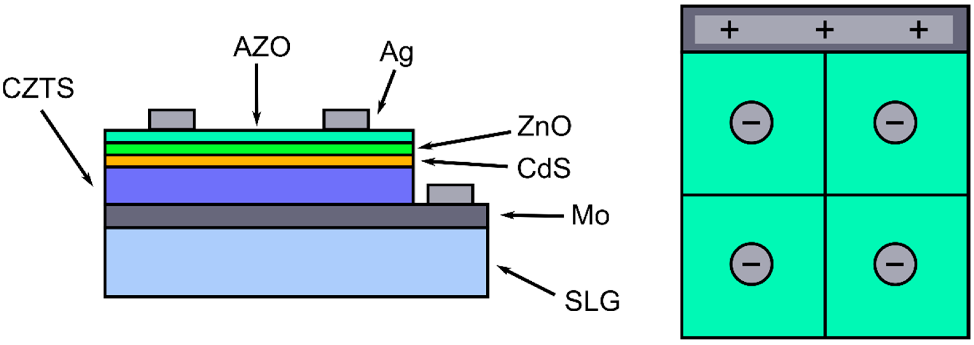
2. Materials and Methods

Within this study, the structural and electrical properties of two identical CZTS/CdS/ZnO/AZO heterostructures were investigated. CZTS/CdS/ZnO/AZO heterostructures were fabricated on glass/Mo substrates cut in 2.5 cm × 2.5 cm dimensions. The CZTS layers were spin-coated at 3000 rpm for 30 s using a solution prepared by dissolving copper(II) chloride (CuCl2), tin(II) chloride (SnCl2), zinc(II) chloride (ZnCl2), and thiourea in a 2-methoxyethanol and monoethanolamine mixture. The ratio of the copper, tin, zinc, and thiourea starting chemicals to each other in the solutions was fixed at 1.8:1.2:1:8. Spin-coated films were dried at 300 °C for 3 min in air. The process was repeated three times to ensure that the initial films reached the desired thickness of ~2 µm. The resultant CZTS thin films were annealed for 30 min in a tube furnace at 550 °C in a nitrogen and sulphur environment [15]. CdS on CZTS was deposited through the chemical bath deposition method using an aqueous solution of cadmium sulfate (0.003 M), thiourea (0.03 M), and ammonia (25%) (1.6 M) at 80 °C for 25 min. The CZTS/CdS structure was then rinsed with pure water and annealed at 200 °C for 10 min. The ZnO and AZO layers were spin-coated at 1500 rpm for 30 s onto the CZTS/CdS structure from the solution prepared by adding 1 g of zinc acetate (and 1 wt% Al for AZO) and monoethanolamine stabilizer (1:1) into 2-methoxyethanol. The fabricated Mo/CZTS/CdS/ZnO/AZO heterostructures were annealed at 200 °C for 60 min. The CZTS/CdS/ZnO/AZO layers were divided into islands by mechanical scribing (~25 mm2). To perform electrical measurements, top contacts (~2.5 mm2) were deposited on top of the AZO layers using silver (Ag) paste. A schematic illustration of the layer structure of glass/Mo/p-CZTS/n-CdS/ZnO/AZO/Ag junctions and the top view of the devices are displayed in Figure 1.
Raman scattering measurements were performed at room temperature using a HORIBA Jobin Yvon T64000 system working in a backscattering geometry and a single subtractive operation mode with a 0.5 cm−1 spectral resolution. The examined samples were firstly excited by a 514.5 nm argon laser with a power of 0.1 mW. The laser exposure time was set to 10 s. Next, by increasing laser power up to 7 mW, one of the samples with a removed CZTS layer was measured. In the following measurement, a 785 nm semiconductor laser was used. The power of the laser beam was set to 8.3 mW, while the laser exposure time was enhanced to 200 s. To obtain I-V curves, a Keithley 2601A I-V source meter was used. AFM data were acquired with the use of a Park Systems XE-70 AFM system.

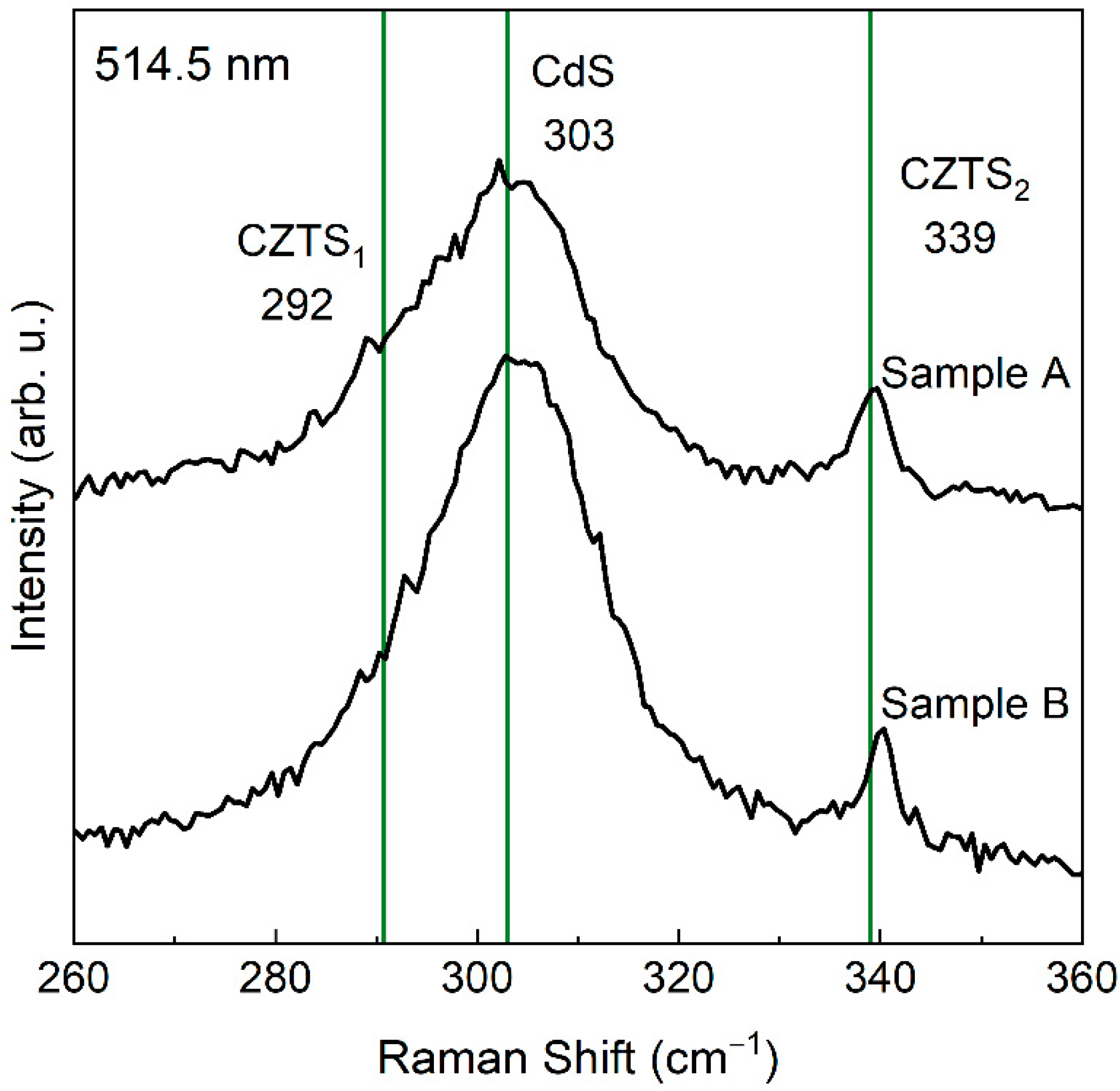
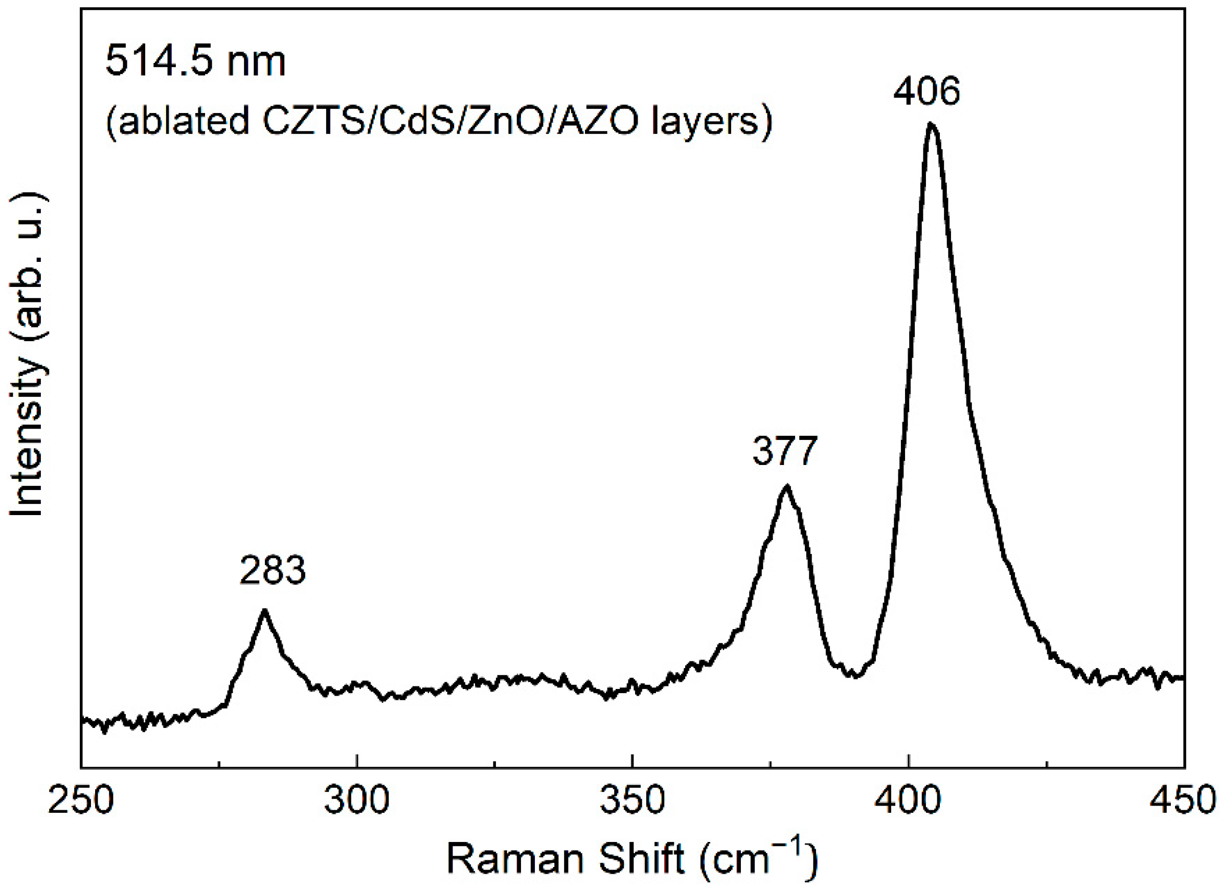
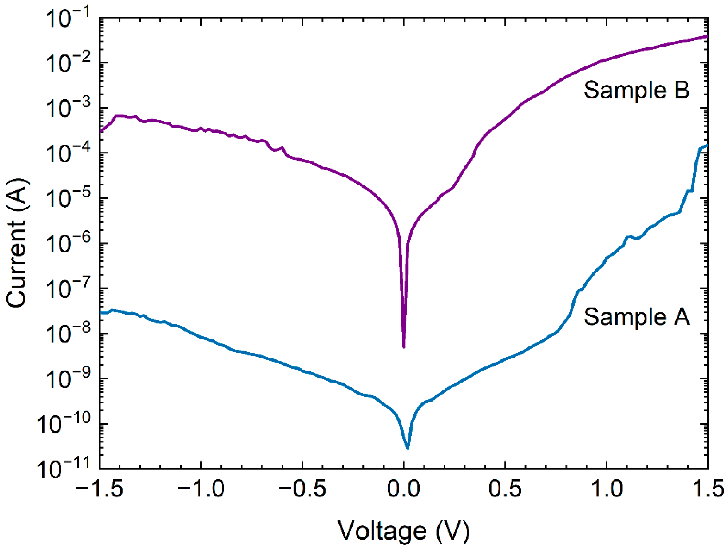
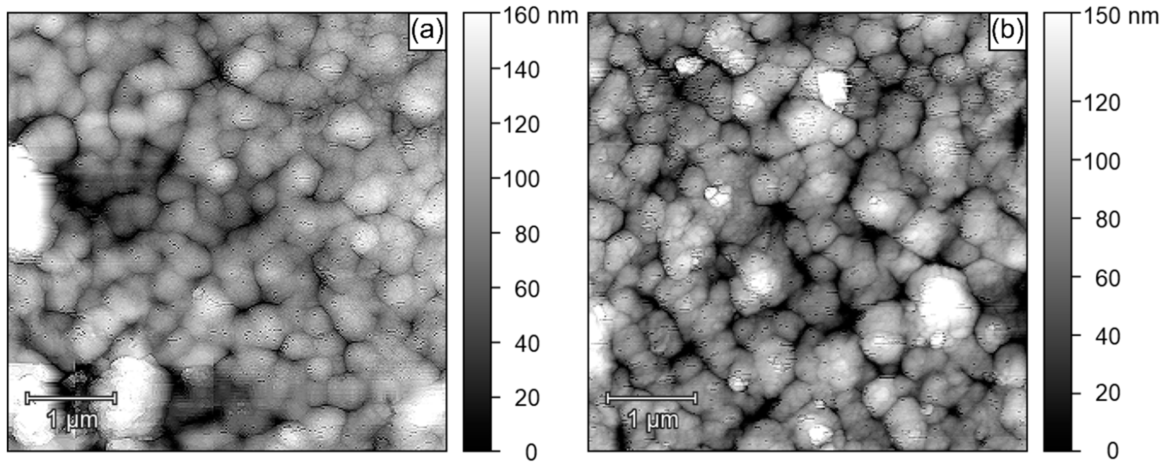
3. Results and Discussion

Figure 2 depicts the Raman spectrum measured for one of the CZTS samples. The data were fitted with three Lorentz functions (blue dotted lines), with the cumulative fit peak (pink solid line) corresponding to the experimental results. One can observe that the Raman spectrum of the investigated sample revealed two well-exposed peaks at 303 and 339 cm−1, and a third one at 288 cm−1, which was found as a result of fitting. The latter peak has the lowest intensity and can be assigned to A-symmetry vibrations of the CZTS crystal structure [18]. Therefore, it is marked as CZTS1. The sharp and narrow CZTS2 peak at 339 cm−1 also has its origin in CZTS. It is related to asymmetrical vibrations of S-atoms [19]. The peak that dominates the spectrum, detected at 303 cm−1, is a few times more intense than the other peaks. It is also significantly broader. This Raman line is from a CdS buffer layer—namely, a longitudinal optical (LO) phonon mode of hexagonal CdS [20].
Figure 3 presents the Raman spectra obtained for the two studied CZTS samples. The approximate position of each observed Raman mode was designated with a green vertical line. As can be seen, the measured spectra do not vary in their characteristics. Considerable differences appear only in their intensity. Table 1 collects peak positions acquired from data pictured on Figure 3. Due to the relatively low intensity of the CZTS1 mode, the determination of the exact peak position was inaccurate. For this reason, the Raman shift of that peak differed from 288 to 296 cm−1, depending on the sample. The results for both CZTS2 and CdS modes were similar for all of the samples.
The use of a 785 nm semiconductor laser to perform Raman measurements delivered significantly different results compared to those obtained with the argon laser. Figure 4 presents the Raman spectrum for one of the CZTS samples, received with a 785 nm excitation wavelength. This time, both the CZTS1 (285 cm−1) and CZTS2 (336 cm−1) modes are clearly distinguishable. A broad Raman band emerges at 367 cm−1. It is related to B or/and E symmetry longitudinal optical (LO) phonons in the CZTS crystal structure [18]. Therefore, it is marked as CZTS3. The CdS-related mode is not present in the spectrum, as for this compound no characteristic Raman line was observed while using a 785 nm laser for excitation [20].
The Raman spectra of all CZTS samples, obtained with an excitation wavelength of 785 nm, do not reveal significant differences. The spectra are dominated by the CZTS modes, as shown in Figure 5. Red solid lines present approximate peak positions for each identified Raman mode. The main dissimilarity between measured spectra was mostly their intensity. The strongest signal was observed for sample B. Therefore, it can be assumed that this sample contained the best-quality CZTS crystal structures. The peak positions gained from the Raman spectra of the analyzed samples are reported in Table 2.
Comparing the values of the Raman mode frequencies collected in Table 1 to those in Table 2, it is clear that some changes occurred in the peak positions. For infrared excitation, the CZTS2 mode is shifted towards lower wavenumbers by 3–4 cm−1. In the case of the CZTS1 Raman band, the situation is more difficult to state, as the mode is weak and almost indistinguishable in one type of spectra and relatively strong in another. However, considering their average positions, they seem to be redshifted as well. Because the CZTS3 band is observed only for a 785 nm excitation wavelength, it cannot be taken into consideration. The most probable explanation for the shift is heating of the structures by laser beam. While using the argon laser, the beam power was set to 0.1 mW, because a higher laser power caused the ablation of the sample. The energy and power of the argon laser could have lead to a relevant increase in the temperature of the sample surface and, therefore, to the observed shift in the peak positions. An analogous situation was observed in the case of II-VI compounds, such as CdTe, ZnTe, and CdZnTe [21]. It was found that the energy of the laser beam above the bandgap of a material heats up the sample and causes damage on the surface, in contrast to the infrared laser [21]. However, in order to verify this hypothesis about the heating of structures, further studies should be performed with Raman Stokes and anti-Stokes measurements, from which the temperature of the surface irradiated by the laser beam can be established. Nevertheless, as mentioned earlier, a higher argon laser power causes the ablation of the sample’s surface.
This study is dedicated to glass/Mo/CZTS/CdS/ZnO/AZO samples which contain spin-coated CZTS thin films. Hence, investigating structures close to the Mo/CZTS interface seems to be crucial in evaluating Mo as an appropriate back contact material for CZTS-based solar cells. The quality of the Mo/CZTS interface is noted for being one of the most significant factors in terms of manufacturing solar cells, which is due to the thermal instability that may result in a MoS2 interlayer [22]. The MoS2 interlayer is known to be a factor that contributes to lowering CZTS-based solar cells’ performance, as it forms a Schottky contact with Mo. Such a structure hampers hole transport from the CZTS layer and leads to the high series resistance of a solar cell, which is highly undesirable [23]. For the purpose of investigating the interface quality, an ablation of CZTS/CdS/ZnO/AZO layers in one of the samples was performed by increasing the argon laser beam power up to 7 mW. Subsequently, a Raman spectrum for the modified sample was measured. The result is presented in Figure 6. The two strongest bands at 377 and 406 cm−1 demonstrate the existence of a MoS2 interlayer on the interface [22]. They are related to E12g and A1g vibrations in the S-Mo-S layers, respectively [24]. The third peak that appears at 283 cm−1 is likely to be an effect of the MoS2 E1g mode [25]. However, the measured spectrum is similar to the one measured for MoS2 microcrystalline powder [26]. In this material, the 283 cm−1 peak matches a (B2g, B3g) vibrational doublet in MoO3, which may be present in the structure due to the relatively high laser beam power (7 mW) used in the measurement, which leads to the oxidation of MoS2 powder [26].
Summarizing the analysis of the Raman studies of the CZTS-based samples, it was shown that no signs of secondary phases were found when using 514.5 nm and 785 nm lasers. Moreover, no Raman bands related to ZnO were identified. Thanks to performing a laser ablation, the formation of an undesirable MoS2 interlayer between Mo and CZTS films was proven, which implied that Mo is not an appropriate back contact material for CZTS-based solar cells.
Dark I-V curves for the CZTS-based diodes in semilogarithmic scale are presented in Figure 7. Table 3 shows the parameters that were calculated on the basis of those experimental data. These are: built-in voltage Vbi, series resistance Rs, rectification ratio RR, and ideality factor n. The diodes differed remarkably in terms of their electrical properties. The highest built-in voltage was measured for sample A (1.40 V). The series resistance ranged from 18.9 Ω (sample B) to 663 Ω (sample A), which is more than a thirtyfold higher value. Sample A seems to have displayed the best rectifying properties, as its rectification ratio at ±1 V (56.8) was significantly higher compared to the other sample. The ideality factors for all of the samples were far more than 1. The p-n junction can be described with a model that assumes occurrence of diffusion or generation-recombination currents. The ideality factor is then in the range of 1 < n 2 [27]. When n > 2 , the charge transport is governed by different current mechanisms, such as the inhomogeneous distribution of recombination centers [28], shunt resistance effects [29], nonlinear metal-semiconductor contacts [30], tunneling currents, and carrier trapping by the surface states or impurities [27,31]. Therefore, it was decided to take a closer look at current transport mechanisms in the junctions by analyzing forward bias I-V curves in double logarithmic scale, as shown in Figure 8.
The plots in Figure 8 are divided into four regions, each one of which represents a different dominant type of current. In the case of the voltage range marked as Region I, the plot is linear and its slope is close to 1. Therefore, Ohm’s law is obeyed, which means that thermal carriers control the current flow in the junction [32]. Region I includes voltages of up to ~0.2 V. In Region II, the plot is non-linear and can be approximated by function I ∼ eA∙V, where A is a constant. This behavior is observed for voltage bias lower than 1 V. It is characteristic for multitunneling capture-emission (MTCE) currents [27]. For higher voltage bias, the linearity of the curve is observed once again (Region III and IV) but this time the slope totals more than two for each sample. As the slope equals two, the space-charge limited current (SCLC) is the dominant charge transport mechanism in the junction. Higher values indicate that there were traps involved in the process [32]. It is worth noting that there appeared to be a rapid increase in current for sample A within the range of 1.4–1.5 V. Such a situation can happen when the voltage bias approaches the trap-filled limit [33].
In order to study the morphology of the studied CZTS-based structures, atomic force microscopy was used. Figure 9 illustrates 2D AFM images for the examined samples. The samples were prepared under the same technological conditions. The surface morphologies of the analyzed samples demonstrate that it is easy to distinguish grains from the samples. They have quite similar structures in terms of grain size. The small difference is probably due to chemical processing. The morphologies discussed above are the standard ones as they are common in the literature [34,35,36]. Table 4 provides the surface roughness parameters calculated from the AFM data.

4. Conclusions

Sol-gel spin-coated glass/Mo/p-CZTS/n-CdS/ZnO/AZO heterojunctions were studied for their structural and electrical properties by means of AFM, Raman scattering, and current–voltage characteristics measurements. AFM disclosed similar surface morphologies among the investigated CZTS-based samples, which differed slightly from each other in terms of grain size as well as roughness. Raman spectroscopy revealed phonon modes at 285 cm−1, 336 cm−1, and 367 cm−1, related to A, B, or/and E symmetry LO phonons in the CZTS crystal structure. An additional Raman mode at 303 cm−1 was ascribed to CdS LO mode. No signs of secondary phases were found while using the 514.5 nm and 785 nm laser. Moreover, the measurements proved the formation of a MoS2 interlayer between CZTS and Mo, confirmed by the occurrence of vibration modes at 283 cm−1, 377 cm−1, and 406 cm−1 in the Raman spectra of the studied samples, obtained at a 514.5 nm excitation wavelength and with an argon laser set to 7 mW. I-V measurements of glass/Mo/p-CZTS/n-CdS/ZnO/AZO diodes also showed rectifying properties of the junctions, as they demonstrated that three different current transport mechanisms can be distinguished from the logI-logV characteristics. These are: thermionic emission of carriers at low voltages, multitunneling capture-emission (MTCE) current, and space-charge limited current (SCLC) at a higher voltage range. The occurrence of MTCE and SCLC currents indicates that there are traps in the studied junctions that are involved in the charge transport process. The type and source of the origin of the traps has not been analyzed within this paper. In summary, in order to obtain high-quality CZTS-based junctions, the control of the structural as well as electrical parameters of CZTS layers is of great importance. Therefore, we believe that the results obtained by us will be crucial for technologists dealing with CZTS-based thin-film solar cells.

Author Contributions

Conceptualization, data curation, writing—original draft preparation, investigation, I.P.; methodology, writing—reviewing and editing, supervision, E.Z.; resources, T.Ö.; validation, H.K. All authors have read and agreed to the published version of the manuscript.

Funding

This research was funded by Çukurova University Research Fund, grant number FBA-2019-11766).

Institutional Review Board Statement

Not applicable.

Informed Consent Statement

Not applicable.

Acknowledgments

This research was partially supported by a statutory grant (No. 8211104160) from the Department of Quantum Technologies at Wroclaw University of Science and Technology, and also partially supported by the Çukurova University Research Fund (Grant No. FBA-2019-11766).

Conflicts of Interest

The authors declare no conflict of interest.

References

  1. Pachauri, R.K.; Allen, M.R.; Barros, V.R.; Broome, J.; Cramer, W.; Christ, R.; Church, J.A.; Clarke, L.; Dahe, Q.; Dasgupta, P.; et al. Climate Change 2014: Synthesis Report; Intergovernmental Panel on Climate Change, IPCC: Geneva, Switzerland, 2014; p. 151. [Google Scholar]
  2. MunichRE. Natural Disaster Risks: Losses are Trending Upwards. Available online: https://www.munichre.com/en/risks/natural-disasters-losses-are-trending-upwards.html (accessed on 5 January 2021).
  3. Allen, J.G.; MacNaughton, P.; Satish, U.; Santanam, S.; Vallarino, J.; Spengler, J.D. Associations of cognitive function scores with carbon dioxide, ventilation, and volatile organic compound exposures in office workers: A controlled exposure study of green and conventional office environments. Environ. Health Perspect. 2016, 124, 805–812. [Google Scholar] [CrossRef] [PubMed] [Green Version]
  4. Fraunhofer Institute for Solar Energy Systems, ISE with support of PSE Projects GmbH. Photovoltaics Report. Available online: https://www.ise.fraunhofer.de/content/dam/ise/de/documents/publications/studies/Photovoltaics-Report.pdf (accessed on 1 May 2020).
  5. Lee, T.D.; Ebong, A.U. A review of thin film solar cell technologies and challenges. Renew. Sustain. Energy Rev. 2017, 70, 1286–1297. [Google Scholar] [CrossRef]
  6. Delbos, S. Kësterite thin films for photovoltaics: A review. EPJ Photovolt. 2012, 3, 35004. [Google Scholar] [CrossRef]
  7. Ito, K.; Nakazawa, T. Electrical and optical properties of stannite-type quaternary semiconductor thin films. Jpn. J. Appl. Phys. 1988, 27, 2094. [Google Scholar] [CrossRef]
  8. Fan, M.S.; Chen, J.H.; Li, C.T.; Cheng, K.W.; Ho, K.C. Copper zinc tin sulfide as a catalytic material for counter electrodes in dye-sensitized solar cells. J. Mater. Chem. A 2015, 3, 562–569. [Google Scholar] [CrossRef]
  9. Rühle, S. Tabulated values of the Shockley-Queisser limit for single junction solar cells. Sol. Energy 2016, 130, 139–147. [Google Scholar] [CrossRef]
  10. Green, M.A.; Dunlop, E.D.; Hohl-Ebinger, J.; Yoshita, M.; Kopidakis, N.; Ho-Baillie, A.W.Y. Solar cell efficiency tables (version 55). Prog. Photovolt. Res. Appl. 2020, 28, 3–15. [Google Scholar] [CrossRef]
  11. Kumar, M.; Dubey, A.; Adhikari, N.; Venkatesan, S.; Qiao, Q. Strategic review of secondary phases, defects and defect-complexes in kesterite CZTS-Se solar cells. Energy Environ. Sci. 2015, 8, 3134–3159. [Google Scholar] [CrossRef]
  12. Dong, L.; Cheng, S.; Lai, Y.; Zhang, H.; Jia, H. Sol-gel processed CZTS thin film solar cell on flexible molybdenum foil. Thin Solid Film. 2017, 626, 168–172. [Google Scholar] [CrossRef]
  13. Agawane, G.L.; Kamble, A.S.; Vanalakar, S.A.; Shin, S.W.; Gang, M.G.; Yun, J.H.; Gwak, J.; Moholkar, A.V.; Kima, J.H. Fabrication of 3.01% power conversion efficient high-quality CZTS thin film solar cells by a green and simple sol-gel technique. Mater. Lett. 2015, 158, 58–61. [Google Scholar] [CrossRef]
  14. Wang, W.; Winkler, M.T.; Gunawan, O.; Gokmen, T.; Todorov, T.K.; Zhu, Y.; Mitzi, D.B. Device characteristics of CZTSSe thin-film solar cells with 12.6% efficiency. Adv. Energy Mater. 2014, 4, 1301465. [Google Scholar] [CrossRef]
  15. Özdal, T.; Kavak, H. Comprehensive analysis of spin coated copper zinc tin sulfide thin film absorbers. J. Alloy. Compd. 2017, 725, 644–651. [Google Scholar] [CrossRef]
  16. Khemiri, N.; Chamekh, S.; Kanzari, M. Properties of thermally evaporated CZTS thin films and numerical simulation of earth abundant and non-toxic CZTS/ZN(S, O) based solar cells. Sol. Energy 2020, 207, 496–502. [Google Scholar] [CrossRef]
  17. Borate, H.; Bhorde, A.; Waghmare, A.; Nair, S.; Pandharkar, S.; Punde, A.; Shinde, P.; Vairale, P.; Jadkar, V.; Waykar, R.; et al. Single-step electrochemical deposition of CZTS thin films with enhanced photoactivity. ES Mater. Manuf. 2021, 11, 30–39. [Google Scholar]
  18. Dimitrievska, M.; Fairbrother, A.; Fontané, X.; Jawhari, T.; Izquierdo-Roca, V.; Saucedo, E.; Pérez-Rodríguez, A. Multiwavelength excitation Raman scattering study of polycrystalline kesterite Cu2ZnSnS4 thin films. Appl. Phys. Lett. 2014, 104, 021901. [Google Scholar] [CrossRef] [Green Version]
  19. Valakh, M.Y.; Litvinchuk, A.P.; Dzhagan, V.M.; Yukhymchuk, V.O.; Havryliuk, Y.O.; Guc, M.; Bodnar, I.V.; Izquierdo-Roca, V.; Pérez-Rodríguez, A.; Zahn, D.R.T. Optical properties of quaternary kesterite-type Cu2Zn(Sn1−xGex)S4 crystalline alloys: Raman scattering, photoluminescence and first-principle calculations. RSC Adv. 2016, 6, 67756. [Google Scholar] [CrossRef] [Green Version]
  20. Saleem, M.F.; Zhang, H.; Deng, Y.; Wang, D. Resonant Raman scattering in nanocrystalline thin CdS film. J. Raman Spectrosc. 2017, 48, 224–229. [Google Scholar] [CrossRef]
  21. Zielony, E.; Płaczek-Popko, E.; Henrykowski, A.; Gumienny, Z.; Kamyczek, P.; Jacak, J.; Nowakowski, P.; Karczewski, G. Laser irradiation effects on the CdTe/ZnTe quantum dot structure studied by Raman and AFM spectroscopy. J. Appl. Phys. 2012, 112, 063520. [Google Scholar] [CrossRef]
  22. Scragg, J.J.; Wätjen, J.T.; Edoff, M.; Ericson, T.; Kubart, T.; Platzer-Björkman, C. A detrimental reaction at the molybdenum back contact in Cu2ZnSn(S,Se)4 thin-film solar cells. J. Am. Chem. Soc. 2012, 134, 19330–19333. [Google Scholar] [CrossRef] [PubMed]
  23. Yang, K.-J.; Sim, J.-H.; Jeon, B.; Son, D.-H.; Kim, D.-H.; Sung, S.-J.; Hwang, D.-K.; Song, S.; Khadka, D.B.; Kim, J.H.; et al. Effects of Na and MoS2 on Cu2ZnSnS4 thin-film solar cell. Prog. Photovolt. 2015, 23, 862–873. [Google Scholar] [CrossRef]
  24. Wu, J.-Y.; Lin, M.-N.; Wang, L.-D.; Zhang, T. Photoluminescence of MoS2 prepared by effective grinding-assisted sonication exfoliation. J. Nanomater. 2014, 2014, 1–14. [Google Scholar]
  25. Fernandes, P.A.; Salomé, P.M.P.; da Cunha, A.F. Study of polycrystalline Cu2ZnSnS4 films by Raman scattering. J. Alloy. Compd. 2011, 509, 7600–7606. [Google Scholar] [CrossRef] [Green Version]
  26. Windom, B.C.; Sawyer, W.G.; Hahn, D.W. A Raman spectroscopic study of MoS2 and MoO3: Applications to tribological systems. Tribol. Lett. 2011, 42, 301–310. [Google Scholar] [CrossRef]
  27. Płaczek-Popko, E.; Paradowska, K.; Pietrzyk, M.; Kozanecki, A. Carrier transport mechanisms in the ZnO based heterojunctions grown by MBE. Opto-Electron. Rev. 2017, 25, 181–187. [Google Scholar] [CrossRef]
  28. Shockley, W.; Queisser, H.J. Detailed balance limit of efficiency of p-n junction solar cells. J. Appl Phys. 1961, 32, 510. [Google Scholar] [CrossRef]
  29. Jain, A.; Kapoor, A. A new method to determine the diode ideality factor of real solar cell using Lambert W-function. Sol. Energy Mater. Sol. Cells 2005, 86, 197–205. [Google Scholar] [CrossRef]
  30. Wang, C.-X.; Yang, G.-W.; Liu, H.-W.; Han, Y.-H.; Luo, J.-F.; Gao, C.-X.; Zou, G.-T. Experimental analysis and theoretical model for anomalously high ideality factors in ZnO/diamond p-n junction diode. Appl. Phys. Lett. 2004, 84, 2427. [Google Scholar] [CrossRef]
  31. Zielony, E.; Płaczek-Popko, E.; Nowakowski, P.; Gumienny, Z.; Suchocki, A.; Karczewski, G. Electro-optical characterization of Ti/Au–ZnTe Schottky diodes with CdTe quantum dots. Mat. Chem. Phys. 2012, 134, 821–828. [Google Scholar] [CrossRef]
  32. Zielony, E.; Przezdziecka, E.; Płaczek-Popko, E.; Lisowski, W.; Stachowicz, M.; Paradowska, K.M.; Jakiela, R.; Kozanecki, A. Deep levels in the MBE ZnO:As/n-GaN diodes—Photoluminescence, electrical properties and deep level transient spectroscopy. J. Alloy. Compd. 2018, 742, 296–303. [Google Scholar] [CrossRef]
  33. Jain, A.; Kumar, P.; Jain, S.C.; Kumar, V.; Kaur, R.; Mehra, R.M. Trap filled limit voltage and V2 law inspace charge limited currents. J. Appl. Phys. 2007, 102, 094505. [Google Scholar] [CrossRef]
  34. Shyju, T.S.; Anandhi, S.; Suriakarthick, R.; Gopalakrishnan, R.; Kuppusami, P. Mechanosynthesis, deposition and characterization of CZTS and CZTSe materials for solar cell applications. J. Solid State Chem. 2015, 227, 165–177. [Google Scholar] [CrossRef]
  35. Li, J.B.; Chawla, V.; Clemens, B.M. Investigating the role of grain boundaries in CZTS and CZTSSe thin film solar cells with scanning probe microscopy. Adv. Mater. 2012, 24, 720–723. [Google Scholar] [CrossRef] [PubMed]
  36. Özdal, T.; Chtouki, T.; Kavak, H.; Figa, V.; Guichaoua, D.; Erguig, H.; Mysliwiec, J.; Sahraoui, B. Effect of annealing temperature on morphology and optoelectronics properties of spin-coated CZTS thin films. J. Inorg. Organomet. Polym. Mater. 2021, 31, 89–99. [Google Scholar] [CrossRef]
Figure 1. A schematic illustration of the layer structure of glass/Mo/p-CZTS/n-CdS/ZnO/AZO junctions and the top view of the device.
Energies 14 05182 g001
Figure 2. Raman scattering spectrum obtained for one of the CZTS samples. The excitation wavelength was 514.5 nm.
Energies 14 05182 g002
Figure 3. Raman spectra for two studied CZTS samples. The excitation wavelength was 514.5 nm.
Energies 14 05182 g003
Figure 4. Raman scattering spectrum obtained for one of the CZTS samples. The excitation wavelength was 785 nm.
Energies 14 05182 g004
Figure 5. Raman spectra for the two studied CZTS samples. The excitation wavelength was 785 nm.
Energies 14 05182 g005
Figure 6. Raman spectrum after performing laser ablation measured with a 514.5 nm excitation wavelength of an argon laser with a power of 7 mW.
Energies 14 05182 g006
Figure 7. Room temperature dark I–V characteristics for the two studied glass/Mo/p-CZTS/n-CdS/ZnO/AZO heterojunctions.
Energies 14 05182 g007
Figure 8. Dark I-V characteristics in double logarithmic scale for two studied glass/Mo/p-CZTS/n-CdS/ZnO/AZO heterojunctions. Each voltage range, marked as Region I–Region IV, stands for a different current transport mechanism.
Energies 14 05182 g008
Figure 9. 2D AFM images of the investigated CZTS-based samples: (a) sample A, (b) sample B.
Energies 14 05182 g009
Table 1. Peak positions (in cm−1) of Raman modes present in the spectra measured with a 514.5 nm excitation wavelength.
CZTS1CdSCZTS2
Mode:A (LO)LO A (LO)
Sample A288303339
Sample B296303340
Table 2. Peak positions (in cm−1) of Raman modes present in the spectra measured with a 785 nm excitation wavelength.
CZTS1CZTS2CZTS3
Mode:A (LO)A (LO)B/E (LO)
Sample A285336367
Sample B285336367
Table 3. CZTS-based diode parameters obtained from the I–V characteristics.
Vbi (V)Rs (Ω)RR at ±1 Vn
Sample A1.40 ± 0.31633 ± 9756.87.363 ± 0.073
Sample B0.802 ± 0.03218.90 ± 0.4033.23.042 ± 0.071
Table 4. Roughness parameters extracted from AFM data: arithmetic average roughness Sa and root mean squared roughness Sq.
SaSq
(nm)(nm)
Sample A2536
Sample B2129
Publisher’s Note: MDPI stays neutral with regard to jurisdictional claims in published maps and institutional affiliations.

