1. Introduction
The automobile industry is undergoing a comprehensive energy transition, and developing electric vehicles has become a clear direction for numerous countries, such as China, those of Europe, and the United States [
1]. Following the advent of intelligent driving, WPT technology has attracted the close attention of numerous scholars and industry researchers due to its advantages, such as safety, reliability, and convenience [
2]. MCRWPT technology adds a resonant compensation network to the transmitting and receiving coils, which solves the problems of high leakage inductance and the low power factor of the system [
3]. At present, this approach is the main technology for wireless power supply of electric vehicles.
Improving the energy transmission efficiency of the WPT system of electric vehicles is a major challenge in current research. In the power electronic system, the application of soft switching technology is an effective method to improve the system efficiency and reduce the interference [
4,
5]. The high-frequency inverter circuit commonly used in the electric vehicle WPT system is a voltage-type full-bridge inverter circuit, whose load is connected with the resonance compensation circuit, which creates the conditions for the realization of the soft switch [
6,
7].
Due to the high operating frequency of the electric vehicle WPT system, which usually reaches the kHz level, when the compensation network reaches the perfectly resonant state (PRS), the diode and MOSFET switching devices in the system cannot be in a perfect soft switching state [
8,
9]. To minimize switching device loss and EMI interference problems, switching devices must be in the ZVS state [
10,
11,
12]. The literature presents three main realization methods of the inverter ZVS: a control strategy, changing the circuit structure, and parameter optimization.
In previous research [
13,
14], the PLL phase-locked loop control method is adopted to realize ZVS. In this approach, the input current of the primary side is collected, the phase difference between the voltage and the current is calculated through zero-crossing detection, and the voltage leads the current by a certain phase by adjusting the opening frequency of the inverter for phase locking. The authors of [
15] proposed a kind of frequency tracking control method in which the circulation size was detected to determine the working frequency and the resonant inverter circuit was used to determine if there was a large deviation from the natural frequency. Then, the controller was used for frequency conversion and decision-making, and to reduce circulation to an acceptable range, and the frequency was set as the work frequency of the inverter to achieve soft switch control.
The authors of [
16] designed a bidirectional WPT system with a ZVS branch with a full-bridge converter. The converter used a branch between switching nodes to provide the ZVS current, and a specially designed modulator was used to obtain an effective ZVS current waveform. The control strategy designed in [
17] includes two control loops. Firstly, the CC or CV operation mode is realized by the phase-shifting control of the full-bridge inverter. Secondly, a branch composed of the MOSFET and capacitor in series is connected in parallel at both ends of the compensating capacitor on the primary side, and the input phase angle is controlled by changing the compensating capacitor value. The DLCC compensation structure was improved in [
18]. ZPA and ZVS are realized by adjusting the compensation capacitance value, and the constant voltage output of the system is realized.
The authors of [
19] proposed a method to realize the ZVS switch of the primary side inverter by optimizing the compensation capacitance value of the secondary side. Simulation and experimental results verified the effectiveness of the proposed compensation network and the setting method. The authors of [
20] proposed a parameter design method for a DLCC compensation network in the phase-shift process of the full-bridge inverter without an auxiliary circuit, identified and analyzed the conditions for realizing ZVS with a lag switch, and verified the analysis results with a 1 kW radio energy transmission prototype.
At present, the method of realizing ZVS using an inverter is not accurate. Furthermore, the influence of parameter changes in the compensation circuit on the realization of ZVS has not been considered comprehensively. A complex closed-loop control strategy is difficult to implement because of signal interference and time response. Due to the shift of the transmitting and receiving coil or the change in the load state, it is difficult to realize the ZVS of the switching tube under a wide range of coupling coefficients and output voltages. Therefore, to improve the transmission power and efficiency of the system, it is particularly important to study the WPT system based on ZVS.
This paper is structured as follows. Firstly, the DLCC compensation circuit is modeled and analyzed, and the expressions of current, voltage, and impedance are obtained, thus laying the foundation for parameter optimization. Secondly, the size parameters of the energy transmitting and receiving coils are determined according to relevant standards, and the influence of the change in the primary and secondary compensation inductance on the circuit element stress and output performance is analyzed to determine the optimal compensation inductance value. Thirdly, the realization condition of ZVS is analyzed, the input impedance expression of the compensation circuit is deduced when the component parameter values are changed, the expression of the inverter output current and circuit parameters is established, and the parameter optimization control strategy for realizing ZVS is proposed. Finally, the effectiveness of the control strategy is verified by establishing a Simulink simulation and experimental platforms.
2. DLCC MCRWPT System Modeling Analysis
The DLCC MCRWPT system structure and mutual inductance equivalent circuit are shown in
Figure 1 and
Figure 2. The system includes a high-frequency inverter circuit, a DLCC resonant compensation circuit (magnetically coupled mechanism), and a rectifier filter circuit.
Uin is the input DC voltage;
S1,
S2,
S3, and
S4 are MOSFETs;
Lf1 and
Lf2 are the primary and secondary compensating inductors, respectively;
Lp and
Ls are the self-inductance of the transmitting coil and the receiving coil, respectively; M is the mutual inductance,
M =
k, where
k is the coupling coefficient between
Lp and
Ls;
C1 and
C2 are series compensation capacitors of primary and secondary sides, respectively; and
Cf1 and
Cf2 are parallel compensation capacitors of primary and secondary sides, respectively.
D1,
D2,
D3, and
D4 are rectifying diodes;
Co represents filtering capacitors of the rectifying circuit;
RL is the load; and
Req is the equivalent load on the secondary side, where
Req = 8
RL/π2.
u1 and
u2 are the input and output voltages of the resonant network, respectively;
if1 and
if2 are the input and output currents of the resonant network, respectively;
ip and
is are the transmitting coil and receiving coil currents, respectively.
Ignoring the parasitic resistances of the capacitor and inductor, and the high-order harmonic components of the voltage of the resonant network, Equation (1) is established according to the mutual inductance equivalent circuit of the system.
The conditions of the full resonance state of the double LCC compensation circuit are as follows:
In the above equation,
ω0 is the resonant angular frequency. According to Equations (1)–(3), we can obtain:
According to Equation (4),
ip and
if2 have independent of the load, and the system has a constant current output characteristic. The output power is as follows:
According to
Figure 2, the total input impedance
Zin, the equivalent impedance
Zs of the secondary side, and the reflection impedance
Zr converted from the secondary side to the primary side of the DLCC compensation circuit are, respectively:
According to the above analysis, it can be concluded that the output characteristics of the DLCC WPT system are mainly related to the parameters of the compensation circuit elements, the coupling coefficient of the transmitting and receiving coils, and the secondary side load. In the following, we optimize the parameters of the system so that the system has a good output characteristic and driving load capacity.
3. Inductance Parameter Optimization Analysis
In this paper, according to the relevant standards of SAE J2954-2020 and GB/T3877, the magnetically coupled mechanism was selected, as shown in
Figure 3, and its 3D model was established based on ANSYS EM.
In the figure, the orange portion is the energy transfer coil, the black plate represents the ferrite core, and the gray area is the aluminum magnetic shielding layer. The specific geometric parameters of the model are shown in
Table 1. In the case that the energy transfer coil is completely aligned (the distance is 20 cm), the simulation results show that the coupling coefficient
k is about 0.2.
The parameters of the DLCC line compensation circuit are generally determined as follows: firstly, the output power level is determined, and the
Lp and
Ls are set appropriately. Then the maximum coupling coefficient is determined, and the compensation inductance
Lf1 and
Lf2 are determined according to Equation (7). Finally, the compensation capacitance is determined according to the resonant condition and the system frequency. The basic parameters of the radio energy transmission system in this paper are shown in
Table 2.
Let
L = Lf1 = Lf2, Lf1×
Lf2 = L2; this indicates that the values of
Lf1 and
Lf2 are not unique, and are defined as:
In theory, Lf1 and Lf2 can be reconfigured by changing the value of σ, assuming that the basic parameters of the system are constant and ensuring that L is constant. According to the above analysis, each σ corresponds to a different set of topological parameters. Therefore, the DLCC compensation circuit can be reconfigured by adjusting the value of σ without changing the basic system parameters. Next, the transmission characteristics of the MCRWPT system under different σ conditions are analyzed to determine the optimal value range of σ.
3.1. Stress Analysis of DLCC Compensation Circuit Elements
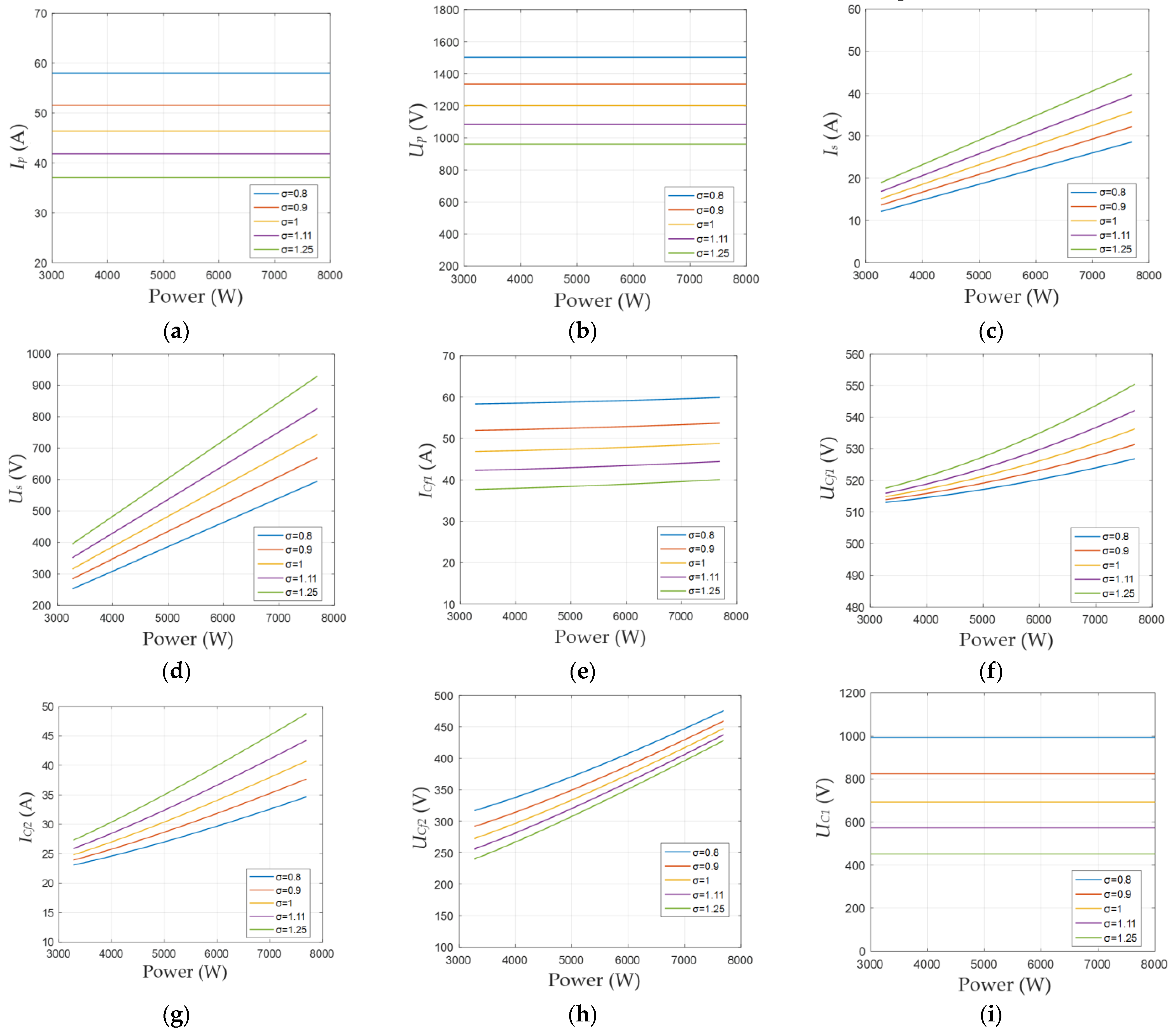
The analysis of the voltage and current stress of the capacitor and the inductor resonant element is a factor that must be considered in compensation circuit design. Excessive voltage and current stress may increase the power loss of the element, affect the energy transmission efficiency of the system, and even damage the equipment. According to
Table 2 and Equation (8), five groups of values of circuit elements under different values of
σ are shown in
Table 3.
According to Equations (4) and (8), and in combination with the parameters in
Table 2 and
Table 3, the variation in voltage and current stress of each element of the DLCC compensation circuit with output power under different
σ values is plotted, as shown in
Figure 4. The current
Ip flowing through the
Lp and the
If2 of the compensation circuit are constant and independent of the output power, which also verifies the constant current output characteristic of the DLCC circuit structure.
If1,
Is,
ICf1,
ICf2,
Us,
UCf1,
UCf2,
UC2, and
Uf1 increase with the increase in output power. Under the same output power condition,
If1 and
If2 do not change with the change in
σ, indicating that the value of
σ does not affect the input and output current characteristics of the double LCC compensation circuit.
Ip,
ICf1,
Up,
UC1,
UCf2, and
Uf2 decrease gradually with the increase in
σ, whereas
Is,
ICf2,
Us,
UCf1,
UC2, and
Uf1 increase gradually. Relatively speaking, the voltage on
Cf1 and
Cf2 does not vary significantly with
σ, whereas the voltage on
C1 and
C2 varies considerable with
σ; thus, the reasonable choice of
σ should be based on the voltage limit of the resonant capacitor. In addition, as the most important component of the MCRWPT system, the magnetically coupling mechanism has a decisive influence on the transmission power and efficiency of the system, and the power loss of this component is an important contributor to the total loss of the system. The loss of the magnetically coupling mechanism is comprised mainly of the coil loss.
Ip and
Is directly determine the size of the coil loss. Therefore, a reasonable choice of the
σ value can reduce the power loss.
3.2. High-Frequency Harmonic Suppression
The voltage waveform of the full-bridge inverter circuit is quantitatively analyzed, and the rectangular wave
u1 with the amplitude of
Uin is expanded into Fourier series, which can be obtained as follows:
As can be seen from Equation (9), the output voltage contains abundant odd harmonics. Although the dual LCC compensation circuit only allows specific resonant frequency components to pass through and has an attenuation effect on the harmonic component, the suppression effect of the high-frequency harmonics is not ideal due to the large number of resonant components in the circuit. Normally, higher harmonics increase switching losses. Because harmonic amplitudes above the fifth order are small, only the fundamental frequencies (85 kHz), the third (255 kHz), and the fifth (425 kHz) are considered. According to the relevant parameters in
Table 2 and
Table 3, the
If1 harmonic content under different
σ values was simulated in Simulink. As can be seen from
Figure 5, with the increase in
σ, the harmonic content of current
If1 was lower. Therefore, to obtain better harmonic suppression performance, the maximum
σ should be used.
4. The Realization of ZVS
The MCRWPT system adopts full-bridge inverter. In practical application, to prevent the circuits of the upper and lower bridge arms from appearing directly and to avoid damage to the switching devices, enough dead time should be set for the switches of the upper and lower bridge arms to ensure the normal operation of the circuit when driving the switch tube of the full-bridge inverter. When the system operates in a completely resonant state, that is, the difference between the input voltage and the current is 0, ZVS is difficult to achieve. To realize ZVS, the input impedance of the system must be inductive. From the perspective of parameter optimization design, in this study, we realized the inverter ZVS under a wide range of coupling coefficients and load changes.
4.1. The Realization Conditions of ZVS
For the case in which the system realizes ZVS, the waveform diagrams of the inverter drive signal, output voltage, and current are shown in
Figure 6, and the commutation process is shown in
Figure 7. The process of turning off
S1 and
S4, and turning on
S2 and
S3, are analyzed as follows.
Prior to
t0,
S1 and
S4 conduct, and
u1 is
Uin. At the stage of
t0–t1,
S1 and
S4 are turned off, the inverter output current
i f1 passes through the junction capacitance of the switch tube, the junction capacitance of
S1 and
S4 (
Coss) charges, the junction capacitance of
S2 and
S3 discharges, and
u1 shows a linear decreasing trend. At the stage of
t1−
t2, the junction capacitors of
S2 and
S3 discharge completely, the voltage at both ends of
S2 and
S3 drops to zero, the current
if1 does not reverse, and the volume diodes of
S2 and
S3 continue to flow. At the moment of
t2, the driving signals of
S2 and
S3 arrive to realize ZVS. At the stage of
t2−
t3,
if1 reverses,
S2 and
S3 conduct, and
u1 is −
Uin. During this process, the dead time
td =
t2 −
t0, during which the current approximately linearly decreases, and the conditions for realizing ZVS of the inverter switch tube, are as follows:
where
itd is the dead zone ending current and
it0 is the shutdown current. When
Coss,
Uin, and
td are determined, the implementation of ZVS is only related to
it0 and
itd.
it0 and
itd are essentially the
if1, so it can be known from Equation (4) that the size of
it0 and
itd is related to the system coupling coefficient, load resistance value, and the compensation circuit element parameters. Therefore, in the case of a wide range of coupling coefficients and load resistances, ZVS can be realized by optimizing the component parameters so that
it0 and
itd always satisfy Equation (10).
4.2. Design of Dead Time
Setting a reasonable dead time is the key to realizing the ZVS inverter. If the dead time setting is too short, a short circuit of the upper and lower bridge arms of the inverter will occur; if the parasitic capacitor impulse current is too large, it may burn out the MOSFET. If the dead time too long, the inverter cannot realize ZVS and generate the impulse current. With the increase in dead time, the output voltage waveform of the inverter is worsened, affecting the transmission efficiency of the system. To ensure the optimal dead time of the inverter MOSFET to realize ZVS, the parasitic capacitor should be fully charged and discharged, and another branch MOSFET should be conducted before the end of the reverse parallel diode continuation current. Thus, the dead time
td should satisfy:
where
tc is the charge and discharge time of the parasitic capacitor,
toff is the MOSFET turn-off time, and
tD is the diode continuation time.
When the model of the MOSFET is determined, the
toff time is determined. The charging and discharging time of the parasitic capacitor,
tc, is:
The diode continuation time,
tD, is:
where
T is the one switching period of the inverter. In practical application, considering that the time of the MOSFET turn-on and turn-off is prolonged due to heat, the optimal dead zone time
td should be relatively large.
4.3. Analysis of the Influence of Resonant Circuit Parameters on Input Impedance Angle
According to Equation (6), the input impedance expression of the compensation circuit is derived when the parameters of complete resonance and inductance, and capacitance, change:
where
Zr = w2M2Cf2Req/Lf2,
C1’,
Cf1’,
Lf1’,
C2’,
Cf2’, and
Lf2’ are the changed circuit component parameter values.
The variation range of the component parameters is set from 0.8 to 1.2. Combined with
Table 2 and
Table 3, and Equation (14), the curve of the circuit input impedance angle, for component parameters under different loads, can be fitted, as shown in
Figure 8. It can be seen from
Figure 8 that, with the change in component parameters, the circuit input impedance angle changes in inductance, resistance, and capacitance. By contrast, changing the values of
C1 and
C2 has a more obvious effect on the impedance angle. As
C1 and
C2 change from small to large, they have the opposite effect on the impedance angle. However, according to Equation (4), changing
C2 affects the constant current output characteristics of the secondary side. Therefore, ZVS is finally realized by changing the value of parameter
C1.
We can take the equivalent resistance
Req = 30 Ω to fit the curve of the change in the circuit input impedance angle with the change in
C1 under different coupling coefficients, as shown in
Figure 9. According to
Figure 8d and
Figure 9, when the value of
C1 is determined (excluding the ratio of 1), with the increase in the coupling coefficient and the load value, the change in the input impedance angle steadily becomes smaller. Therefore, as long as the value of
C1 satisfying ZVS is determined in the case of the maximum coupling coefficient and the maximum load value, ZVS in the full range of coupling coefficients and loads can be realized.
According to Equation (10), the value of
it0 +
itd is determined by
Coss,
Uin, and
td. Therefore, the relationship between
it0,
itd, and
C1 needs to be clarified to obtain the optimized value of
C1. The high-order harmonics of the current
if1 are ignored. The phase difference between the fundamental voltage of the compensation circuit and the input fundamental voltage is defined as
α, and the expressions of
it0 and
itd are obtained by combining with Equation (1).
Therefore, according to Equations (10) and (15)–(18), the value of C1 satisfying ZVS can be calculated.
4.4. Parameters Optimization Control Strategy
According to the analysis in the above section, after optimizing the basic parameters of the WPT system, when the load and coupling coefficient change, the inverter can theoretically be guaranteed to work in the ZVS state at all times. However, due to the progress in the wireless charging process of electric vehicles, the temperature of the magnetically coupled mechanism and compensation circuit will inevitably rise, and the system parameters will change. This will result in interference in the inverter output voltage and the current waveform. Although this change will not have a significant impact on the system, it is likely to change the working state of the inverter ZVS. When the MCRWPT system works normally, the circuit parameters cannot be changed. It can be seen from Equations (10) and (15)–(18) that the working state of the inverter can only be adjusted by changing the dead time td and frequency f of the inverter.
Because the output voltage and current of the inverter will not mutate, the dynamic adjustment of the dead zone time does not require a high speed. Thus, the control is carried out by adjusting the dead zone and frequency with a fixed-length step. The MCRWPT system control block diagram and parameter optimization control flow chart are shown in
Figure 10 and
Figure 11, respectively.
6. Conclusions
The MCRWPT system studied in this paper has a high power grade, and the DLCC topology has better anti-migration and power transmission stability. Based on the DLCC topology, this study proposed a parameter optimization control strategy based on frequency and dead time to improve power transmission efficiency. Without changing the circuit structure, ZVS in a wide range of voltage classes was realized. This method comprehensively considers the influence of parameter changes on the implementation of ZVS, can be simply controlled, and overcomes the shortcomings of the ZVS implementation method, as noted in
Section 1.
First, a DLCC equivalent circuit model was established, and the expressions of output voltage, current, and input impedance were derived. Second, five sets of component parameter values were obtained according to the changes in the primary and secondary side compensation inductance values. The suppression effect of the circuit component stress and high-frequency harmonics under different parameters was analyzed, and the optimal compensation inductance value was determined. Third, the realization conditions of ZVS were analyzed, the best dead time of the MOSFET was determined, and the change in the system input impedance angle with different component parameter values was obtained. The relationship between the inverter output current and the capacitor C1 was established, and the optimal capacitor value was determined through simulation. Finally, a parameter optimization control strategy to achieve ZVS was proposed. Under different output power levels, the average efficiency of the PRS was 90.87%, the average efficiency of ZVS was 91.86%, indicating an increase in efficiency of about 1%.
Therefore, the parameter optimization strategy of the DLCC MCRWPT system based on ZVS can reduce the power loss of the MOSFET, effectively improve the charging efficiency, and promote the development of WPT technology. This strategy can be applied to high-power WPT systems, such as robots and electric vehicles, and has certain practical significance.


 ,
, 


