Article

Independent Upper- and Lower-Arm Switching Scheme Based on Reference Current Polarity for Three-Level NPC Inverters

1
Research and Development Center, Willings. Co., Ltd., Chobu-ro 54 beongil, Yongin-si 17037, Korea
2
Department of Electrical Engineering, Yuhan University, Gyeongin-ro 590, Bucheon 14780, Korea
3
Department of Information and Communication Engineering, Yuhan University, Gyeongin-ro 590, Bucheon 14780, Korea
*
Author to whom correspondence should be addressed.
Energies 2021, 14(17), 5535; https://doi.org/10.3390/en14175535
Submission received: 30 June 2021 / Revised: 6 August 2021 / Accepted: 30 August 2021 / Published: 4 September 2021
(This article belongs to the Special Issue Optimal Design of Power Converters)

Abstract

:
This study presents a novel switching scheme for three-level neutral point clamped (NPC) inverters. The proposed switching method independently drives the upper- and lower-arm elements of the inverter based on the polarity information of the reference current. The proposed switching scheme does not require the inclusion of dead-time for each switching, except when the current polarity changes. Therefore, unlike the conventional inverter switching method, dead-time compensation is not needed, and the possibility of an arm-short accident is prevented. In this study, a switching procedure is detailed, and the operation mode analysis of the proposed switching scheme is presented. The effectiveness of the proposed switching method is verified experimentally by application to a grid-connected inverter that requires inverter current control.

1. Introduction

Three-level inverters are widely used for medium- and large-capacity inverters. As three-level inverters have good performance and efficiency, they also have complex circuits and controls. In the case of a three-level inverter having a neutral point, the voltage applied to the switching element is halved compared to that of a two-level inverter. In addition, since the three-level inverter has a smaller current ripple than the two-level inverter, it is advantageous as a grid-connected inverter, where the problem of harmonics included in the output current is important. Therefore, studies on three-level inverters have been continuously investigated [1,2]. In the case of H-bridge-type power converters, which are driven by a conventional complementary switching method, when the switching elements of the upper- and lower-arm are turned on simultaneously, an arm-short of the DC link occurs. Therefore, in order to prevent an arm-short, dead-time must be inserted into all switching signals. For the perfect prevention of an arm-short, sufficient dead-time is required. However, when the dead-time is inserted, output waveform distortion is generated due to errors generated during the dead-time. Therefore, various studies have investigated dead-time compensation, such as extracting and compensating harmonics generated by dead-time or adjusting the effective application time according to the current direction [3,4]. The dead-time compensation in the three-level neutral point clamped (NPC) inverter is also compensated by analyzing the dead-time effect similar to the dead-time compensation used in the two-level inverter [5,6,7,8,9,10].
Furthermore, dead-time elimination methods have been proposed, which do not need to insert the dead-time according to the current polarity [11,12,13]. In these cases, there is a problem in accurately detecting the polarity of the actual current. An alternative switching method capable of operating without dead-time by driving a switching device according to the polarity of the reference current in the two-level inverter has been proposed [14]. This method is useful for the current control system.
In the case of a three-level NPC inverter, a study that eliminates the dead-time by dividing the switching modes according to the polarity of the voltage reference and the polarity of the actual current has been proposed [15,16]. However, if the polarity of the actual current cannot be accurately detected, there is a possibility of an arm-short when the current polarity is switched.
A method using the voltage of the IGBTs has also been proposed to detect the actual current polarity accurately, but it has a disadvantage in that an additional circuit must be added in parallel to the IGBTs [17].
In the current study, a new switching method for a three-level NPC inverter is proposed. Since the proposed switching method independently switches the upper- and lower-arm elements based on information on the polarity of the reference current rather than the actual current, sensing of the actual current is not involved; therefore, the proposed method is easily applicable. Moreover, the possibility of an arm-short does not exist, and dead-time compensation is not required.
The detailed switching strategy and operation mode analysis of the proposed switching method are described, and the effectiveness of the proposed switching method is verified by applying it to a 1 MW grid-connected photovoltaic power generation system.
The authors state that this paper is based on a preliminary version [18] presented at the RTUCON conference in Riga, Latvia, in 2019.

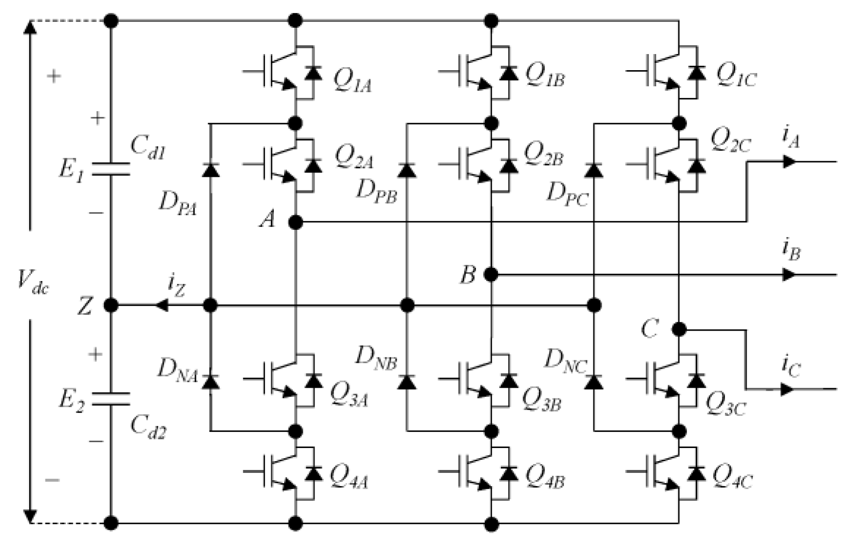
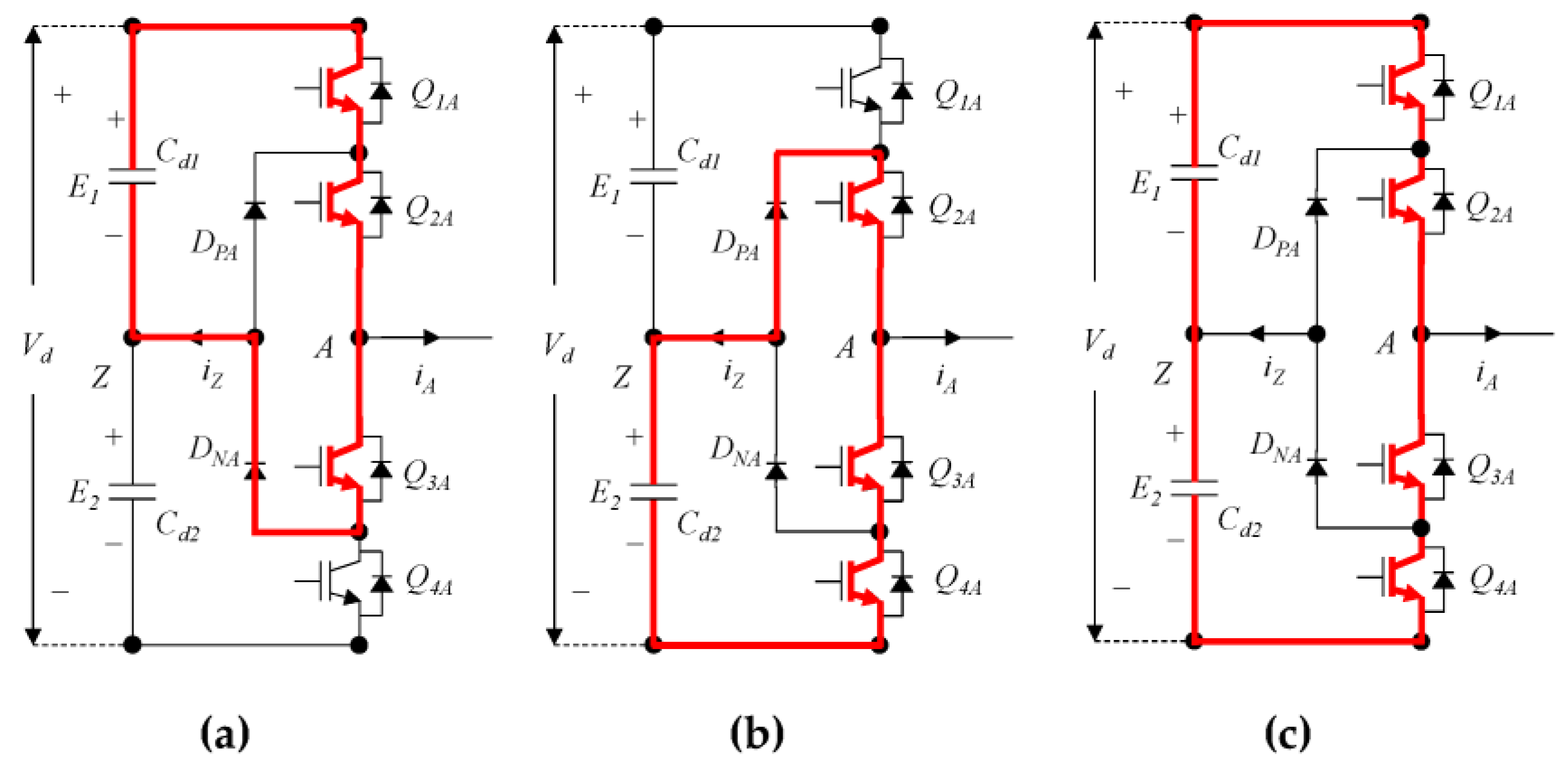
2. 3 Phase Three-Level NPC Inverter

Figure 1 shows the circuit of a typical NPC three-level inverter; as shown in the figure, four switches and two clamping diodes constitute one arm. A clamping diode is connected to the neutral point Z between the DC link capacitors depending on the operating switching state and is used to clamp the output voltage to zero.
Table 1 depicts the switching mode of the conventional switching method and the on/off state of the switch according to the inverter output voltage. In switching mode P, the two upper switches are turned on so that the voltage VAZ between point A and neutral point Z becomes +E1. In switching mode N, the two sub-switches are turned on so that VAZ becomes E2. In switching mode O, switches S2 and S3 are turned on, and the output voltage across the clamping diode is zero. Switch pairs S1 and S2 operate in a complementary manner with S3 and S4.
Figure 2 shows the waveform of the switching signal of the phase opposition disposition (POD) modulation scheme, which is a conventional carrier-based switching signal scheme. It can also be generated via other PWM methods, including space vector PWM. Whichever method is used, when S1, S2, and S3 are operated simultaneously, an arm-short occurs as shown in Figure 3a. Alternatively, an arm-short occurs when S2, S3, and S4 are turned on simultaneously (Figure 3b). In rare cases, an arm-short is possible when all the switching elements are turned on (Figure 3c).
As previously mentioned, when an H-bridge-type power converter is driven using the conventional PWM switching method in a complementary manner without dead-time, a short-circuit occurs in the DC link. Therefore, the dead-time needs to be included to prevent an arm-short, as depicted in Figure 4. In the figure, Dap and Dan are reference signals, tp and tn are the turn-on time of S1 and S4, respectively, and td is the dead-time. S1~S4 are switching signals, and G1~G4 are gate signals with the dead-time. As a result, it can be observed that the modulation error occurs in the output voltage during dead-time, compared to the ideal case, which necessitates compensation to reduce the voltage error and harmonics caused because of the dead-time.

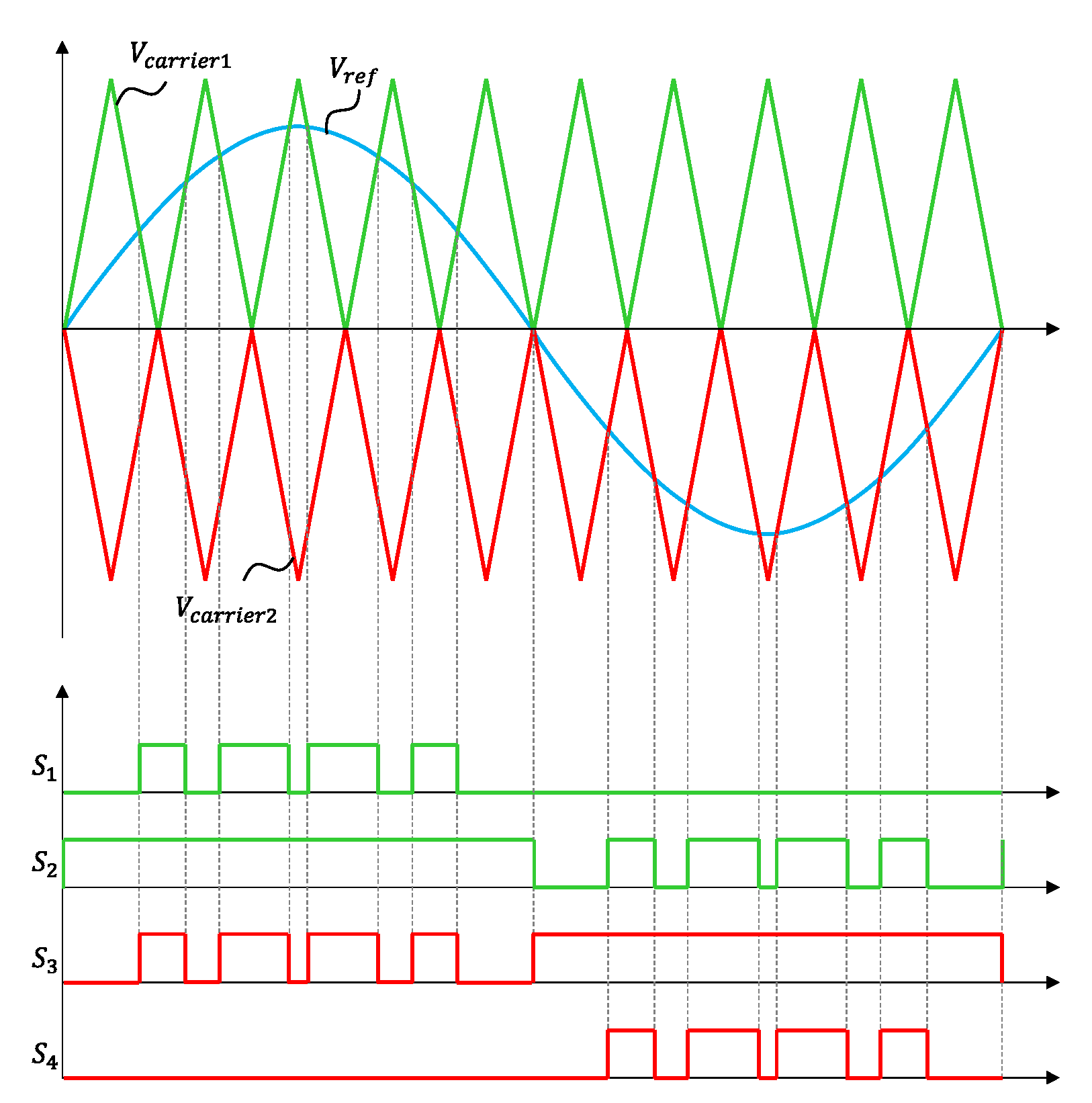
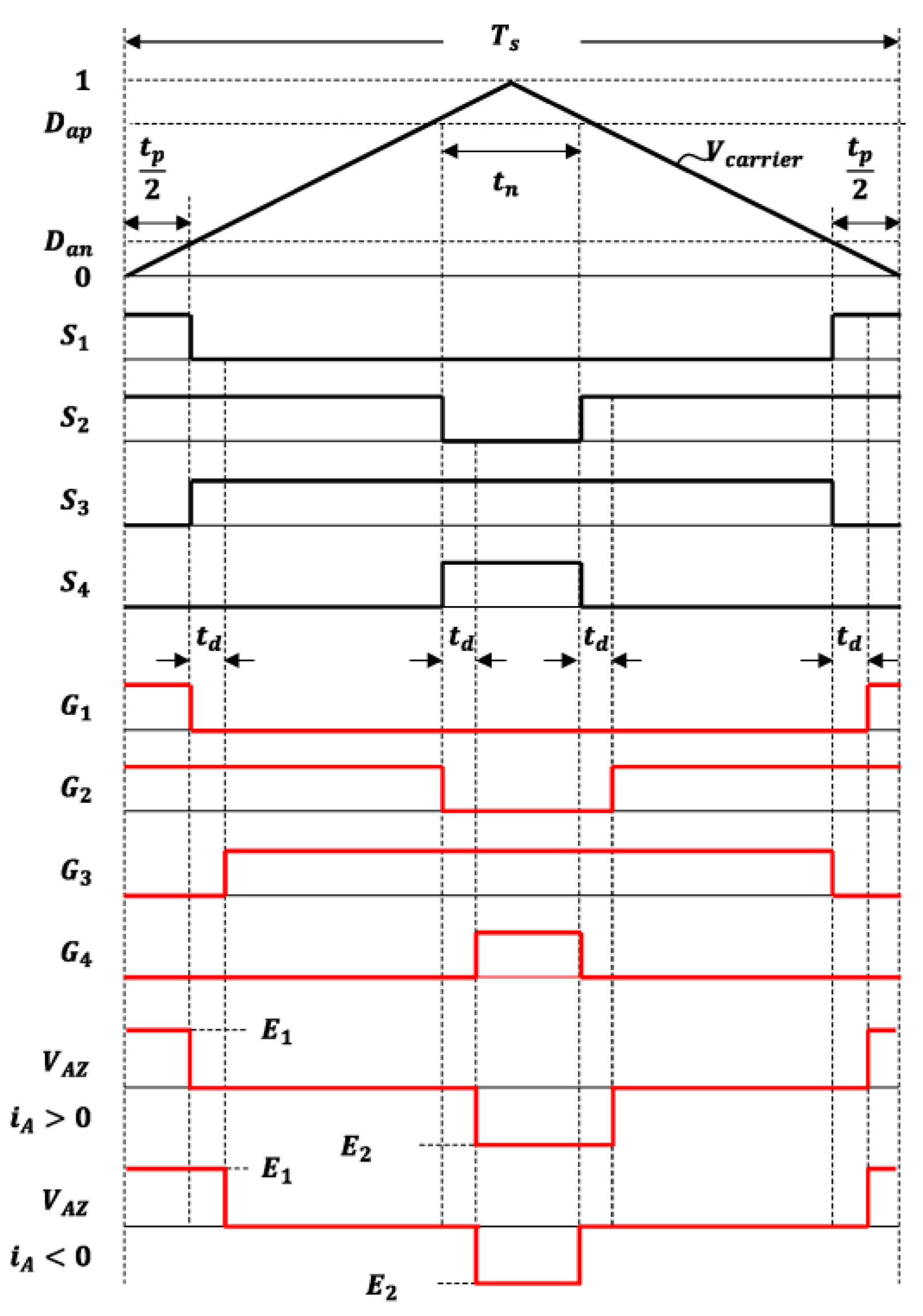
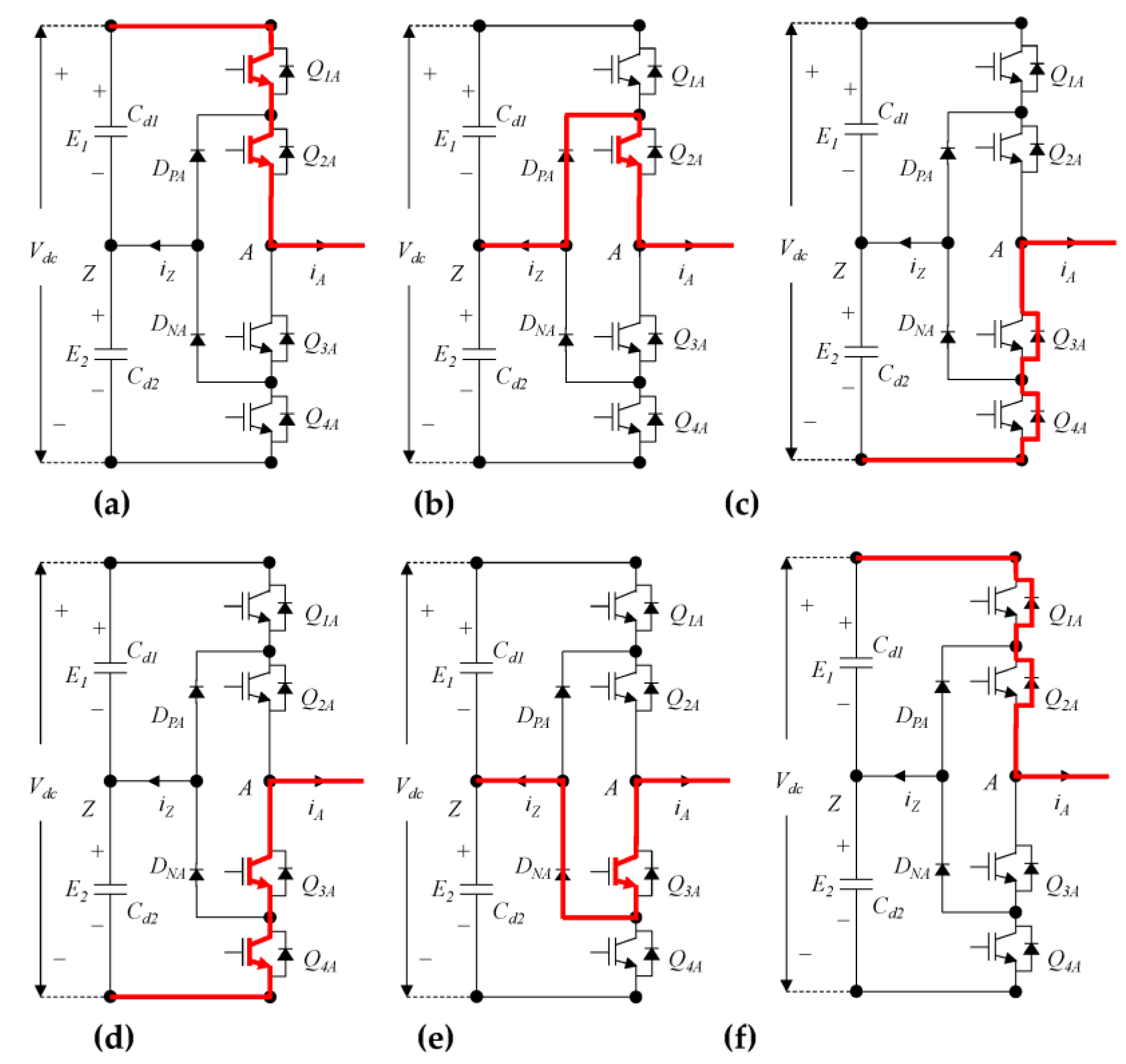
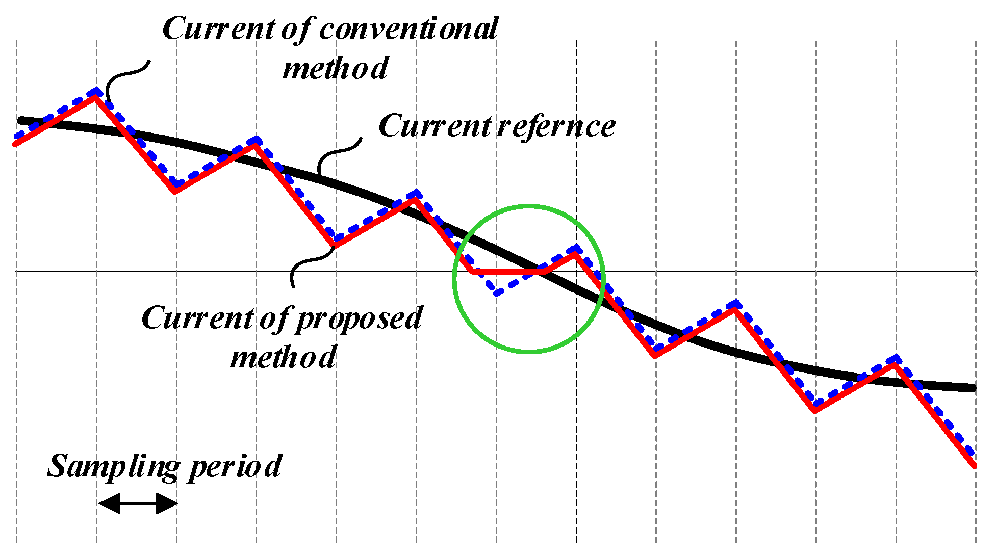
3. Proposed Switching Scheme

In this study, we present a novel switching method of three-phase NPC three-level inverters that selects a switching device using the polarity information of the reference current. The grid-connected PV system or motor driving system is controlled by the current control method.
Therefore, the selection of switching elements can be used for the information about the reference current polarity rather than the actual current.
Figure 5 shows the proposed switching signal generation scheme. The method of generating the primary switching signals S1, S2, S3, and S4 is the same as the conventional POD modulation method:
S 1 = { 1 w h e n V c m d V c p 0 w h e n V c m d < V c p ,
S 4 = { 1 w h e n V c m d V c n 0 w h e n V c m d > V c n ,
S 2 = { 1 w h e n V c m d > V c n 0 w h e n V c m d V c n = S 4 ¯                                                                 ,
S 3 = { 1 w h e n V c m d < V c p 0 w h e n V c m d V c p = S 1 ¯                                                                 ,
where Vcmd is the output voltage command, and Vcp and Vcn are carrier signals.
The switching devices are determined for each operation mode according to the reference current polarity, as follows:
S 1 = C R P   &   S 1 ,
S 2 = C R P   &   S 2 = C R P   &   S 4 ¯ ,
S 3 = C R P ¯   &   S 1 ¯ ,
S 4 = C R P ¯   &   S 4 ,
where
C R P = { 1 w h e n C u r r e n t R e f e r e n c e 0 0 w h e n C u r r e n t R e f e r e n c e < 0 .
Dead-time DP and DN are determined for gate signals G1 and G4, respectively. DP is the dead-time from the negative-going transition (NGT) of S3, whereas DN is the dead-time from the NGT of S2′. Although DP and DN are determined, they are not always adopted.
Therefore, the final gate signal can be obtained as follows:
G 1 = D P   &   S 1 = D P & C R P   &   S 1 ,
G 2 = S 2 = C R P   &   S 4 ¯ ,
G 3 = S 3 = C R P ¯   &   S 1 ,
G 4 = D N   &   S 4 = D N   &   C R P ¯ & S 4 .
Figure 6 depicts the hardware implementation of the proposed switching scheme. In the conventional switching method, the hardware for inserting the dead-time includes four one-shot and four AND-gates. In the hardware implementation of the proposed method, two one-shots are reduced, and two AND-gates and one NOT-gate are added, simplifying the circuit.
Table 2 shows the status of the switching elements in the conduction mode for the proposed switching method. Mode O in the conventional switching method (Table 1) is divided into modes PO and NO according to the polarity of the voltage and current. In addition, a new mode OO is presented in which all the switches are turned off.
The current path of each conduction mode for phase A is shown in Figure 7. From Figure 7, only Q1A and Q2A are turned on when the current is positive, and only Q3A and Q4A are turned on when the current is negative. Therefore, dead-time is no longer required, except when the polarity of the reference current is changed.
Table 3 depicts the operation mode according to the conduction mode, which is determined by the output voltage polarity and the reference current polarity. Table 4 shows the conduction mode from phase X to phase Y, i.e., when the XY line current is positive. Here, X and Y denote A and C, respectively. According to the conduction mode of each phase, a total of nine modes are possible.
In Equations (10) and (13), the dead-time for switching Q1 and Q4 is determined when the polarity of the reference value is changed. The determined dead-time may or may not be applied depending on the switching conditions. Even if the dead-time is applied, it is shorter than the determined dead-time, and is applied just once when the polarity of the reference current is changed. Moreover, during this time, no dead-time compensation is required in the current control system as the actual current is near zero.
However, if the polarity of the reference current is changed before the polarity of the actual current, the current discontinuity may occur near-zero current in the proposed switching scheme, as depicted in Figure 8; hence, the proposed switching method is not recommended for systems where the output current is not significant compared to the ripple current caused by switching.

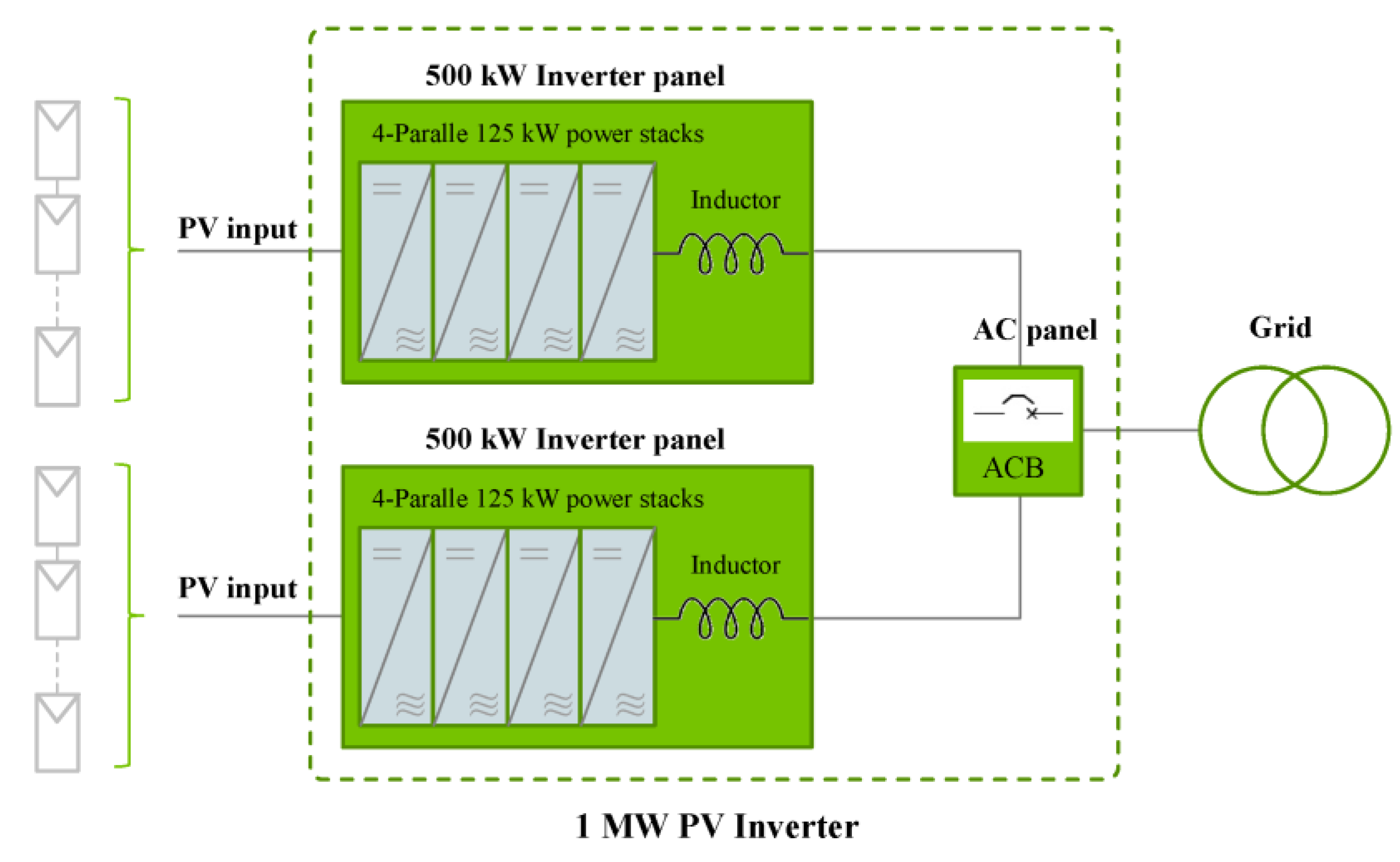
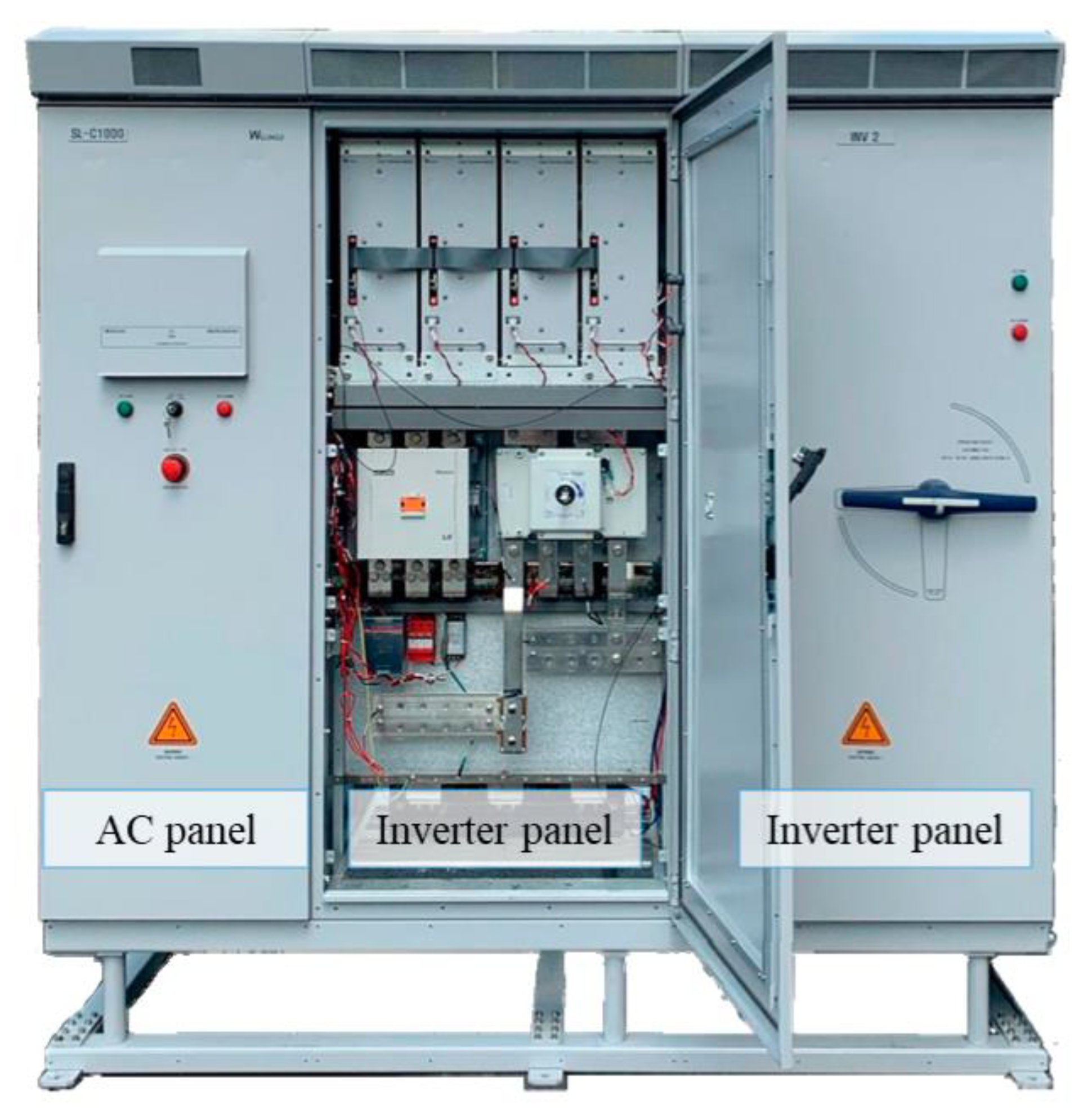
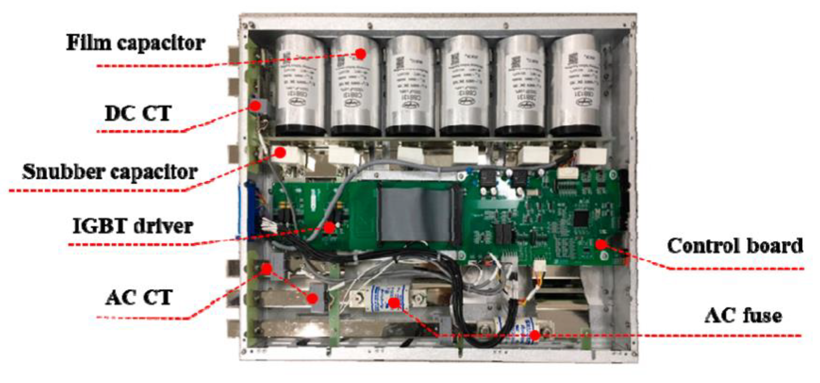
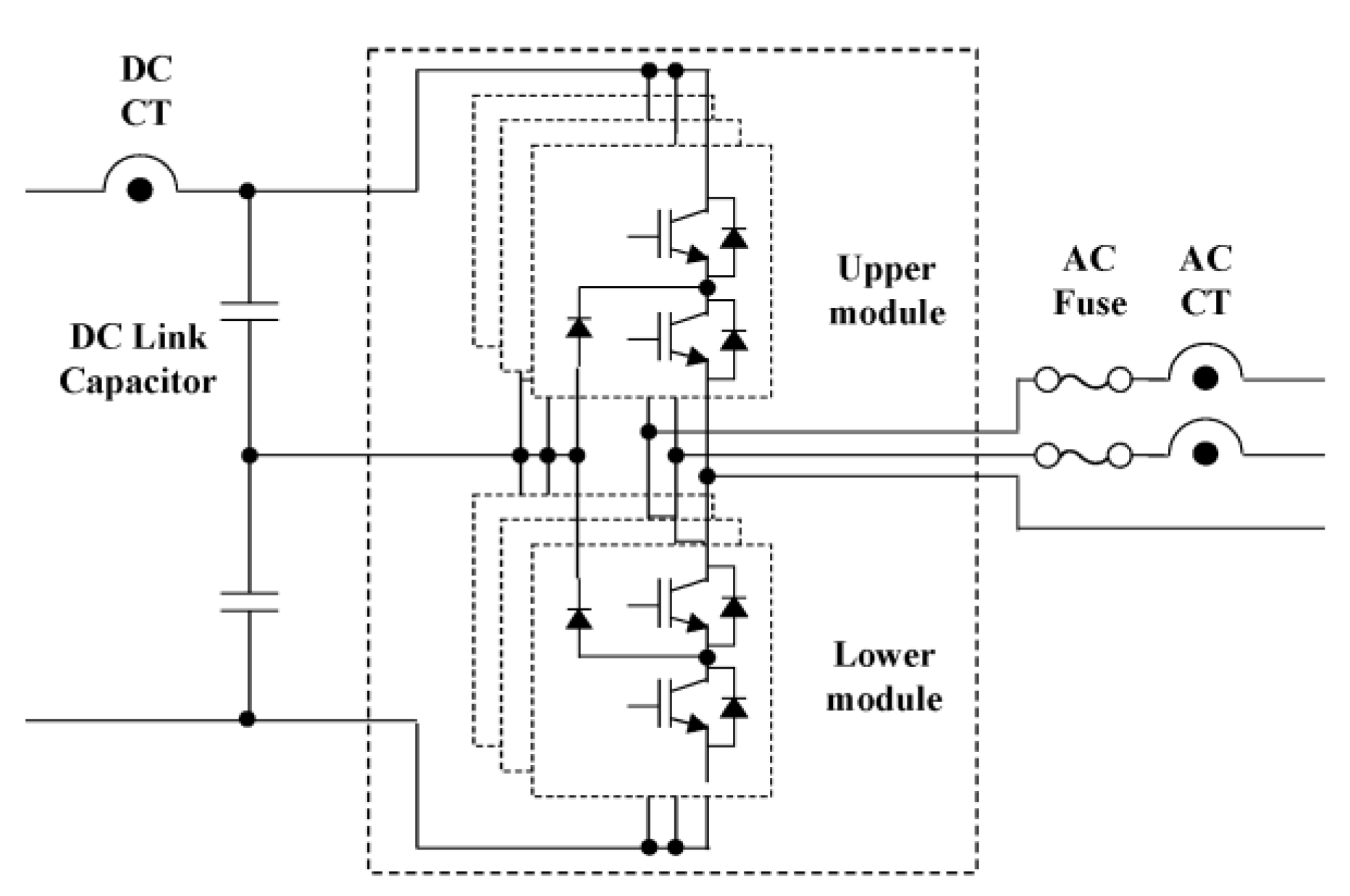
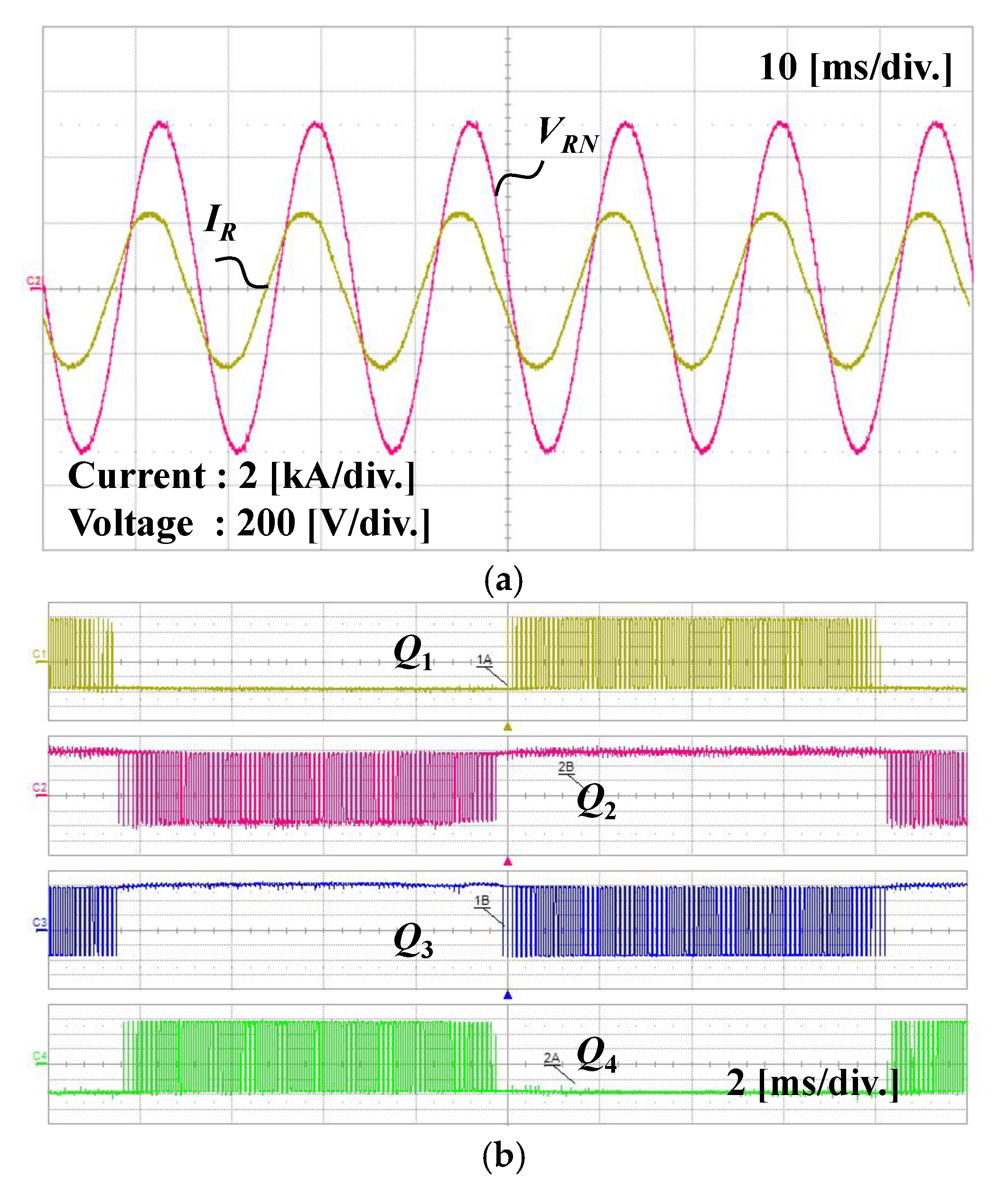
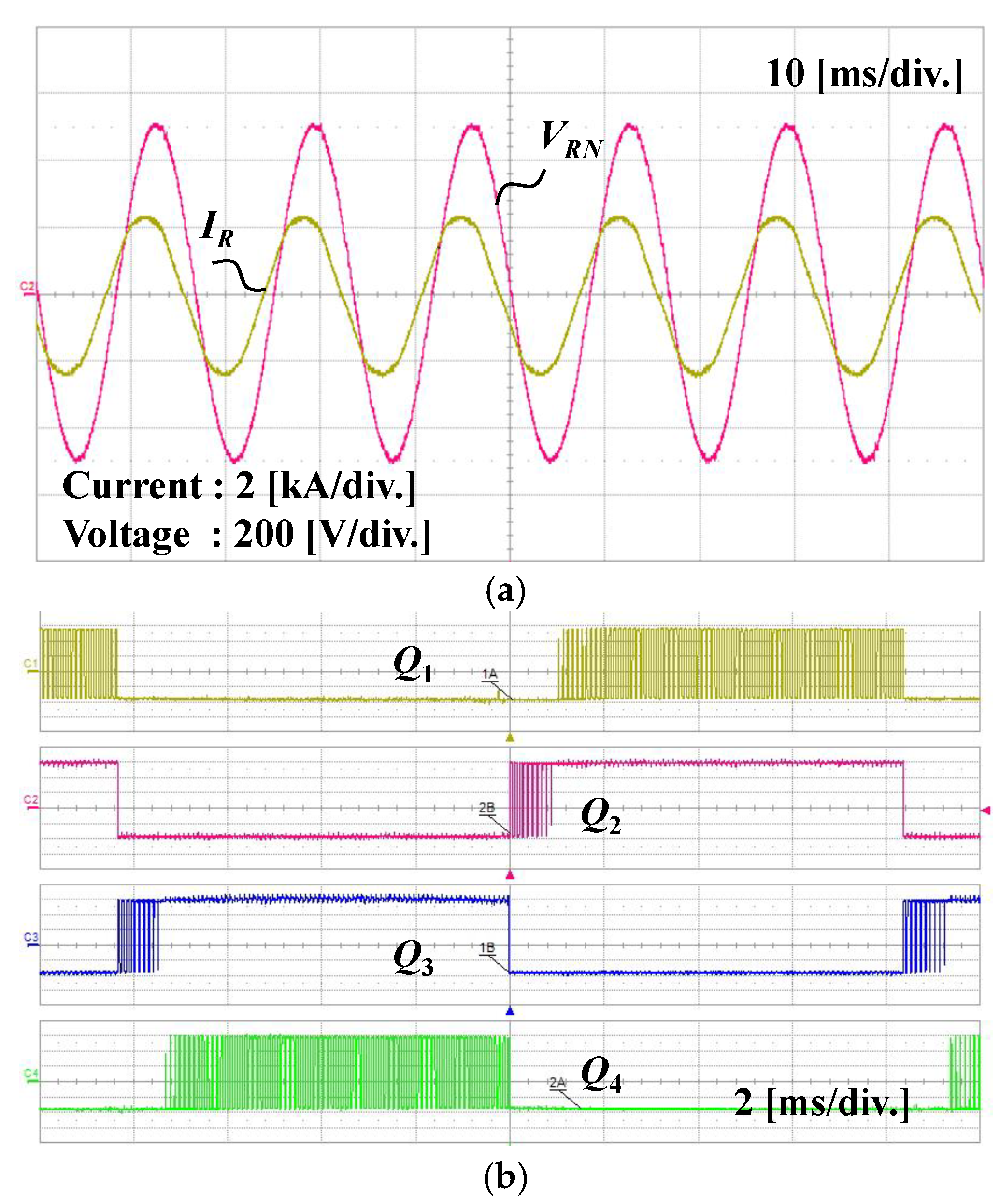
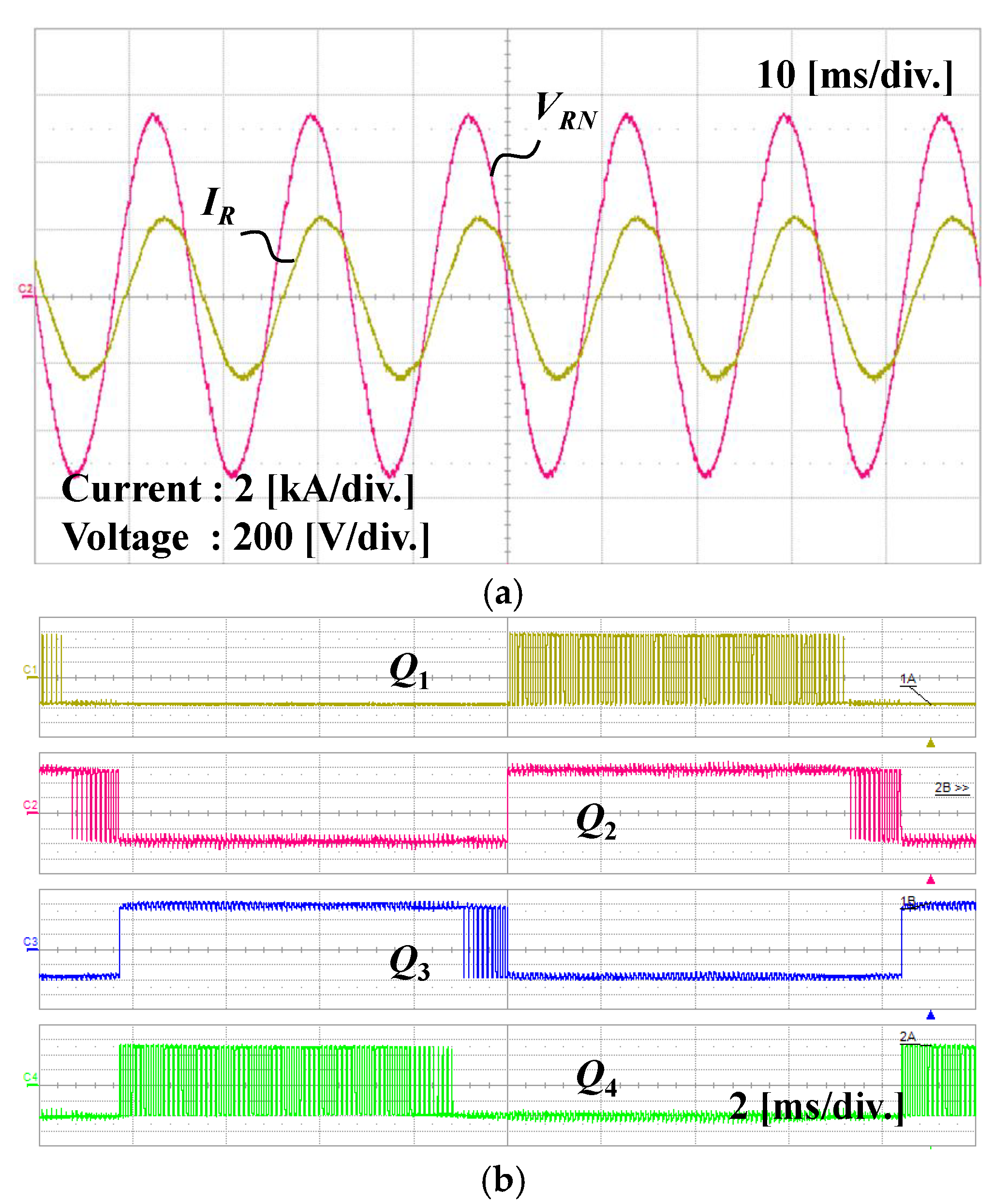
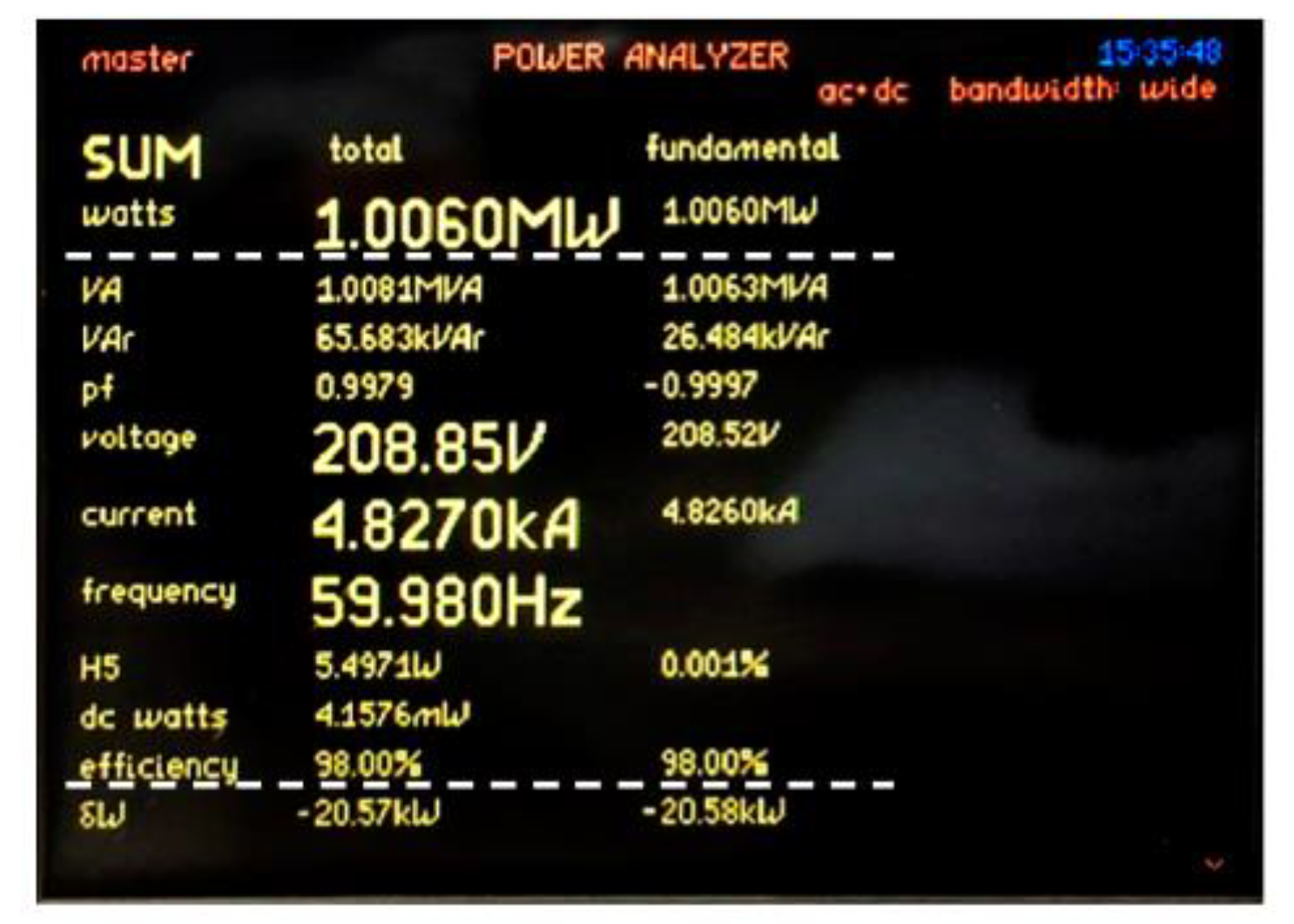
4. Experimental Results

An experiment was conducted to confirm the effectiveness of the proposed switching scheme by applying it to a 1 MW grid-connected photovoltaic (PV) system, as shown in Figure 9. The 1 MW PV inverter is a multi-central type, with two 500 kW inverter panels in parallel. Each inverter panel consists of four 125 kW power stacks connected in parallel, and the same switching signals drive each power stack. Figure 10 displays the image of the 1 MW PV inverter system used in the experiment. Table 5 shows the detailed specifications of the 1 MW grid-connected PV inverter proposed in this study.
Figure 11 displays the image of the 125 kW power stack, and Figure 12 presents the circuit for one of the arms. The ratings of the main components of the 125 kW power stack and 500 kW inverter panel are shown in Table 6 and Table 7, respectively.
The total harmonic distortion (THD) measurement results indicate that the proposed switching method has lesser THD than the conventional switching method with dead-time compensation. This may be because the adopted dead-time compensation method may be not perfect. If the dead-time compensation is perfect, there are no differences in the harmonic characteristics, but this is nearly impossible.
Figure 13 and Figure 14 depict the experimental results obtained using the conventional switching method and the proposed switching scheme, respectively. Figure 13a and Figure 14a show the waveforms of the grid voltage and the output current of the inverter system, whereas Figure 13b and Figure 14b depict the gate signals. In this case, the grid voltage and inverter output current are in phase, so the power factor of the grid is in unity. However, the inverter output current is slightly lagged from the inverter output voltage due to the filter inductance between the inverter output stage and the grid; thus, mode of operation II (Table 3) exists in the vicinity of the change in polarity of the current from positive to negative. Comparison of the current waveforms shows that there is no difference between the proposed switching method and the conventional switching method with dead-time compensation.
Figure 15 and Figure 16 show the experimental waveforms when the power factor of the system was controlled to 0.9, whereas Figure 17 and Figure 18 show the experimental waveforms when the power factor was controlled to −0.9. The power factor was controlled through d-axis current control. This shows that the proposed switching method implements well, whether the current is lagging or leading. Therefore, when the proposed switching method is adopted, the possibility of an arm-short is eliminated, and dead-time compensation is not required.
Figure 19 is an enlarged waveform of the output current and gate signal when the power factor is 1.0. However, the inverter output current is slightly lagged from the output voltage due to the filter inductance between the grid and the inverter output stage. Therefore, it can be observed that operation mode II (Table 3) exists at the instant wherein the polarity of the current changes from positive to negative.
Figure 20 and Figure 21 show the experimental results when the phase of the output current is controlled to be the same as the phase of the grid voltage when the PV output voltage is 750 V, the grid voltage is 340 V, and the inverter output power is 1 MW. In Figure 20, the conventional switching method with dead-time compensation is used, whereas in Figure 21, the proposed scheme is used. It can be observed that there are no differences in the experimental result of the conventional switching method that requires dead-time compensation and the proposed switching scheme. This proves that arm-short accidents can be prevented with the proposed switching scheme, and dead-time compensation is no longer required.
The THD measurement results indicate that the THD of the proposed switching method is lesser than that of the conventional switching method with dead-time compensation. This may be because the adopted dead-time compensation method is not perfect. If dead-time compensation is perfect, there are no differences in the harmonic characteristics, but this is nearly impossible.
Figure 22 shows the result of measuring the efficiency of the power, and it was measured to be 98% at the 1 MW rated output. Since the proposed method only reduces the gate drive power to half compared to the conventional method, the efficiency improvement is not significant.

5. Conclusions

A novel switching scheme that independently drives the upper- and lower-arm elements of an inverter using the polarity information of the reference current instead of the polarity information of the actual current was proposed in this study. The proposed switching scheme does not require the inclusion of dead-time for every switching signal, except at the instant at which the reference current polarity changes. Therefore, dead-time compensation is not required with the proposed switching scheme. In addition, it prevents arm-short circuit accidents and reduces the gate drive power to half. However, the proposed switching scheme can be applied only to a current control system because it requires the polarity information of the reference current. The switching procedure was detailed, and an operation mode analysis of the proposed switching scheme was presented. An experiment was performed to verify the effectiveness of the proposed switching scheme by applying it to a multi-central type 1 MW grid-connected inverter system. The obtained results established that with the proposed switching scheme, arm-short accidents can be prevented, and dead-time compensation is no longer required.

Author Contributions

Conceptualization, K.A. and K.C.; methodology, K.A. and Y.O.; software, Y.O.; validation, W.O. and K.C.; writing—original draft preparation, Y.O. and K.C.; writing—review and editing, W.O. and K.C. All authors have read and agreed to the published version of the manuscript.

Funding

This research received no external funding.

Institutional Review Board Statement

Not applicable.

Informed Consent Statement

Not applicable.

Data Availability Statement

Not applicable.

Conflicts of Interest

The authors declare no conflict of interest.

References

  1. Shibata, N.; Tanaka, T.; Kinoshita, M. Development of a 3.2MW Photovoltaic Inverter for Large Scale PV Power Plants. In Proceedings of the 2018 International Power Electronics Conference (IPEC-Niigata 2018 ECCE Asia), Niigata, Japan, 20–24 May 2018; p. 39293933. [Google Scholar]
  2. Yan, C.; Xu, D. Design Study of MW Photovoltaic Inverter. In Proceedings of the 2018 IEEE International Power Electronics and Application Conference and Exposition (PEAC), Shenzhen, China, 4–7 November 2018; p. 16. [Google Scholar]
  3. Li, H.; Li, Y.; Ge, Q. Dead Time Compensation of 3Level NPC Inverter for Medium Voltage IGCT Drive System. In Proceedings of the IEEE 35th Annual Power Electronics Specialists Conference, Aachen, Germany, 20–25 June 2004; p. 35243528. [Google Scholar]
  4. Dolguntseva, I.; Krishna, R.; Soman, D.; Leijon, M. Contour Based Dead-Time Harmonic Analysis in a Three-Level Neutral Point Clamped Inverter. IEEE Trans. Ind. Electron. 2015, 62, 203210. [Google Scholar] [CrossRef]
  5. Jing, G.; Xuegeng, G.; Feng, Z.; Xuhui, W. A Strategy Novel Dead-time Compensation of Three-level Inverter. In Proceedings of the IEEE Transportation Electrification Conference and Expo, Beijing, China, 31 August–3 September 2014; p. 15. [Google Scholar]
  6. Piao, C.; Hung, J. Analysis and Compensation of Dead-Time Effect in Multi-Level Diode Clamped VSI Based on Simplified SVPWM. In Proceedings of the 2015 IEEE 10th Conference on Industrial Electronics and Applications, Auckland, New Zealand, 15–17 June 2015; p. 375380. [Google Scholar]
  7. Li, X.; Akin, B.; Rajashekara, K. Vector Based Dead-Time Compensation for Three-Level T-Type Converters. IEEE Trans. Ind. Appl. 2016, 52, 15971607. [Google Scholar]
  8. Wang, S.; Song, W.; Ma, J.; Zhao, J.; Feng, X. Study on Comprehensive Analysis and Compensation for the Line Current Distortion in Single-Phase Three-Level NPC Converters. IEEE Trans. Ind. Electron. 2018, 65, 21992211. [Google Scholar] [CrossRef]
  9. Niu, J.; Chen, R.; Zhang, Z.; Gui, H.; Wang, F.; Tolbert, L.; Blal, B.; Costinett, D.; Choi, B. Analysis of Circulating Harmonic Currents in Paralleled Three Level ANPC Inverters using SVM. In Proceedings of the 2019 IEEE Applied Power Electronics Conference and Exposition, Anaheim, CA, USA, 17–21 March 2019; p. 24812487. [Google Scholar]
  10. Sprenger, M.; Alvarez, R.; Bernet, S. Direct Dead-Time Control—A Novel DC-Link Neutral-Point Balancing Method for the Three-Level Neutral-Point-Clamped Voltage Source Inverter. In Proceedings of the 2012 IEEE Energy Conversion Congress and Exposition, Raleigh, NC, USA, 5–20 September 2012; p. 11571163. [Google Scholar]
  11. Kulkarni, A.; Mazumder, S. Deadtime Elimination in a GaN-Based Grid-Connected Differential-Mode Ćuk Inverter. IEEE Trans. Ind. Electron. 2019, 66, 32963302. [Google Scholar] [CrossRef]
  12. Yuan, J.; Zhao, Z.; Chen, B.; Li, C.; Wang, J.; Tian, C.; Chen, Y. An Immune-Algorithm-Based Dead-Time Elimination PWM Control Strategy in a Single-Phase Inverter. IEEE Trans. Power Electron. 2015, 30, 39643975. [Google Scholar] [CrossRef]
  13. Yan, Q.; Zhao, R.; Yuan, X.; Ma, W.; He, J. A DSOGI-FLL-Based Dead-Time Elimination PWM for Three-Phase Power Converters. IEEE Trans. Power Electron. 2019, 34, 28052818. [Google Scholar] [CrossRef]
  14. Cho, K.; Oh, W.; Kim, Y.; Kim, H. A New Switching Strategy for Pulse Width Modulation (PWM) Power Converters. IEEE Trans. Ind. Electron. 2007, 54, 330337. [Google Scholar] [CrossRef]
  15. Kan, Y.; Hyun, S.; Hong, S.; Won, C. Zero Deadtime PWM Implementation Method for Reducing Total Harmonic Distortion in 3Level NPC Inverter. In Proceedings of the 2015 18th International Conference on Electrical Machines and Systems (ICEMS), Pattaya, Thailand, 25–28 October 2015; p. 10691073. [Google Scholar]
  16. Hyun, S.; Hong, S.; Won, C. A Compensation Method to Reduce Sampling Delay of Zero Dead-Time PWM Using 3Level NPC PWM Inverter. In Proceedings of the 2016 IEEE Transportation Electrification Conference and Expo, Asia-Pacific (ITEC Asia-Pacific), Busan, Korea, 1–4 June 2016; p. 465469. [Google Scholar]
  17. Alawieh, H.; Riachy, L.; Tehrani, K.; Azzouz, Y.; Dakyo, B. A New Dead-Time Effect Elimination Method for H-bridge Inverters. In Proceedings of the 42nd Annual Conference of the IEEE Industrial Electronics Society, Florence, Italy, 23–26 October 2016; p. 31533159. [Google Scholar]
  18. Ahn, K.; Oh, Y.; Cho, K. A Study on the Development of a 1 MW Grid-Connected Photovoltaic Inverter System. In Proceedings of the IEEE 60th International Scientific Conference on Power and Electrical Engineering of Riga Technical University (RTUCON), Riga, Latvia, 7–9 October 2019; p. 19. [Google Scholar]
Figure 1. Circuit of a typical NPC three-level inverter.
Energies 14 05535 g001
Figure 2. Switching signal waveforms of the conventional phase opposition disposition (POD) modulation scheme.
Energies 14 05535 g002
Figure 3. Current path of the short circuit for phase A: (a) transition of mode-P and mode-O; (b) transition of mode-N and mode-O; (c) transition of mode-P and mode-N.
Energies 14 05535 g003
Figure 4. Waveforms of the conventional switching signal with dead-time and the output terminal voltage.
Energies 14 05535 g004
Figure 5. Proposed switching signal generation scheme.
Energies 14 05535 g005
Figure 6. Logical diagram of the proposed switching scheme.
Energies 14 05535 g006
Figure 7. Current path of each conduction mode for phase A: (a) PP mode; (b) PO mode; (cOO mode (iA > 0); (d) NN mode; (e) NO mode; (f) OO mode (iA < 0).
Energies 14 05535 g007
Figure 8. Occurrence of current discontinuity.
Energies 14 05535 g008
Figure 9. 1 MW PV system used in the experiment.
Energies 14 05535 g009
Figure 10. Image of the 1 MW PV inverter system.
Energies 14 05535 g010
Figure 11. Image of the 125 kW power stack.
Energies 14 05535 g011
Figure 12. Schematic of one of the arms of the 125 kW power stack.
Energies 14 05535 g012
Figure 13. Experimental results in the case where the power factor is controlled at 1.0 using the conventional switching method: (a) waveforms of the output voltage and current; (b) waveforms of the gate signal.
Energies 14 05535 g013
Figure 14. Experimental results in the case where the power factor is controlled at 1.0 using the proposed switching scheme: (a) waveforms of the output voltage and current; (b) waveforms of the gate signal.
Energies 14 05535 g014
Figure 15. Experimental results in the case where the power factor is controlled at 0.9 (lag) using the conventional switching method: (a) waveforms of the output voltage and current; (b) waveforms of the gate signal.
Energies 14 05535 g015
Figure 16. Experimental results in the case where the power factor is controlled at 0.9 (lag) using the proposed switching scheme: (a) waveforms of the output voltage and current; (b) waveforms of the gate signal.
Energies 14 05535 g016
Figure 17. Experimental results in the case where the power factor is controlled at −0.9 (lead) using the conventional switching method: (a) waveforms of the output voltage and current; (b) waveforms of the gate signal.
Energies 14 05535 g017
Figure 18. Experimental results in the case where the power factor is controlled at −0.9 (lead) using the proposed switching scheme: (a) waveforms of the output voltage and current; (b) waveforms of the gate signal.
Energies 14 05535 g018
Figure 19. Magnified waveforms of the current and gate signals in the case of a unity power factor at the grid: (a) waveforms of the conventional switching method; (b) waveforms of the proposed switching scheme.
Energies 14 05535 g019
Figure 20. Experimental results of the conventional switching method: (a) current waveforms; (b) THD of the current; (c) harmonic analysis.
Energies 14 05535 g020
Figure 21. Experimental results of the proposed switching scheme: (a) current waveforms; (b) THD of the current; (c) harmonic analysis.
Energies 14 05535 g021
Figure 22. Efficiency measurement result at the 1 MW rated output.
Energies 14 05535 g022
Table 1. Switching mode of the conventional switching method.
Switching
Mode
Switching SignalExpected Inverter Terminal Voltage
VAZ
S1S2S3S4
POnOnOffOffE1
OOffOnOnOff0
NOffOffOnOnE2
Table 2. Conduction mode.
Conduction ModeSwitch StatusTerminal Voltage
VAZ/VBZ/VCZ
Q2Q2Q3Q4
PPOnOnOffOffE1
POOffOnOffOff0
OOOffOffOffOffE1 (I < 0)/−E2 (I > 0)
NOOffOffOnOff0
NNOffOffOnOnE2
Table 3. Operation mode.
Operation
Mode
Current
Reference
Polarity
Voltage
Polarity
Conduction
Mode
Mode-IPositivePositivePP/PO
Mode-IIPositiveNegativePO/OO
Mode-IIINegativeNegativeNN/NO
Mode-IVNegativePositiveNO/OO
Table 4. Conduction mode from phase A to phase C.
A-C
Conduction
Mode
Conduction
Mode of
Phase A
Conduction
Mode of
Phase C
A-C
Line to Line
Voltage
Mode-1PPNNE1 + E2
Mode-2PPNOE1
Mode-3PPOO0
Mode-4PONNE2
Mode-5PONO0
Mode-6POOOE1
Mode-7OONN0
Mode-8OONOE2
Mode-9OOOOE1E2
Table 5. Specification of the 1 MW PV inverter system.
ItemValue
InputPV voltage (max)1000 V
Operation voltage range550–1000 V
MPPT voltage range550–1000 V
PV current (max)1652.8 A
OutputPower1000 kW
Frequency60 Hz (59.3–60.5)
Voltage340 V (3Φ3W)
Current (max)1698 A
ETCOperating temperature−20–50 °C
IP degreeIP44
CoolingForced air
Table 6. Ratings of the major parts for the 125 kW Power stack.
ItemValue
DC CT300 A
DC link capacitor1000 μF/700 V × 3P2S
IGBT Module (upper)650 V/400 A × 3 EA
IGBT Module (lower)650 V/400 A × 3 EA
AC Fuse700 V/300 A
AC CT300 A
Table 7. Rating of the major parts for the 500 kW inverter panel.
ItemValue
Power stack125 kW × 4P
DC Fuse630 A, 1000 V × 2P
DC SPD1000 V/40 kA
DC EMI CoreNano crystal/200 mm
DC Switch1000 A/1000 V
Filter inductor0.1 mH/1000 A
Filter capacitor40 μF/450 V × 4P
MC1260 A/1000 V
Publisher’s Note: MDPI stays neutral with regard to jurisdictional claims in published maps and institutional affiliations.

