Article

Is It Possible to Obtain Benefits by Reducing the Contribution of the Digital Signal Processing Techniques to the Control of the Active Power Filter?

Faculty of Electrical and Computer Engineering, Cracow University of Technology, 31-155 Cracow, Poland
Energies 2021, 14(19), 6031; https://doi.org/10.3390/en14196031
Submission received: 16 August 2021 / Revised: 16 September 2021 / Accepted: 18 September 2021 / Published: 22 September 2021

Abstract

:
This paper presents a simple yet efficient control method for active power filters that can be used to improve power quality. Applying this method can open the way towards limiting the hardware and computational expenditure, which are needed for control of the active filter, while maintaining its required performance. The method is based on the indirect approach of obtaining reference signals combined with the closed-loop current control technique. Monitoring of changes of energy stored in reactance elements of the active filter is the base for obtaining reference signals for compensation. The active filter can perform classical compensation and, additionally, can perform some extra functionality for managing of active power in the system. In particular, it can stabilize the supplying source power, enable energy exchange between loads connected on DC and AC sides of the active filter, and—in a case of generating loads—enable their energy storage and redistribution amongst consuming loads. The presented method can be useful for voltage-source as current-source inverter based active filters, and for DC systems as well as for AC single- or three-phase ones.

1. Introduction

Specifically controlled power electronic converters are widely used to improve power quality. They are then called active filters or compensators. In this role, they compensate for undesirable components of current and/or voltage waveforms of the supply source. Such compensation consists of generating these components by the active filter and forcing them through the supply sources, according to reference signals developed in real time.
The active filter can be considered as a combination of two basic modules: the measurement and control module (signal processing module) and the executing module (power processing module).

1.1. Measurement and Control Module (Signal Processing Module)

The measurement and control module work out reference signals, which are then used as the input information for the power processing module. These references arise as a result of measurements of selected current and voltage waveforms after their transformation in accordance with a specific control algorithm. It should be emphasized that the selection for tracing and processing a certain subset of the total number of current/voltage waveforms of the whole system is associated with fundamental decisions related to the functional properties of the active filter.
There are review papers containing an exhaustive classification of control methods, algorithms, and control circuit structures [1,2,3,4,5]. Generally, control methods for active filters are classified as either Time-domain or Frequency-domain methods. Additionally, a wide group of unconventional (from today’s point of view) reference-generation techniques are distinguished. They are often called “Other” methods, including a dynamically growing subgroup of so-called learning techniques.
Time-domain nonactive current components extraction approaches offer a relatively small number of calculations, significantly higher speed of achieving reference signals, and increased robustness compared to other extraction methods. Other advantages of time-based methods include relative ease of implementation, resistant to wide-band noise and sensor distortions, and very good steady-state performance if the supply voltage is of high quality. On the other hand, there are some drawbacks of this method. The most important are reported as sensitivity to distortion and imbalance in the supply source voltages and lags in real-time compensation [3]. For the time-domain methods, the following specific implementation techniques may be distinguished [2]: synchronous fundamental dq frame, synchronous individual harmonic dq frame, instantaneous power pq theory and variants, and generalized integrators and variants.
Frequency-domain algorithms used for finding nonactive current components are based on Fourier analysis. Once these components are extracted from the measured signals, they are transformed back to time-domain reference signals. For this two-stage procedure, a relatively long time as well as high-quality hardware are required to ensure efficient performance. However, the advantage of this method is flexibility in the selection of nonactive components of supply current (considered as its higher harmonics—which is a certain limitation) for compensation [6,7].
In the frequency-domain methods, there are the basic reference-generation techniques discussed [2,3]: fast Fourier transform (FFT), discrete Fourier transform (DFT), recursive discrete Fourier transform (RDFT), and wavelet-based approach. It should be noted that selective compensation is possible not only for frequency-domain methods. There exists a number of different techniques suitable for this purpose. Then, when considering the full spectrum of nonactive components of the total load power, the selective compensation enables to control the active filter strategy to operate without overstepping its maximum rated current [8,9,10].

1.2. Active Filter with Reduced Number of Sensors

In many articles minimizing the number of current and voltage sensors, which are needed to obtain reference signals for compensation, are considered as important (probably one of the first articles on this topic was [11]). The resulting benefits are reduced digital hardware costs, lower complexity of computational algorithms for DSP-based control implementation, and easier calibration of the entire compensation system. Emphasis is placed on the reduction of the number of current sensors [12,13,14,15,16].
Consequently, efforts are made to avoid the need to monitor the load current. In such a situation, the frequency techniques are often abandoned in favor of time-domain ones. This naturally leads to the direct achievement of the goal of compensation, which is to obtain the assumed parameters of the supply source current in closed-loop control scheme [17,18,19,20].
The positive effect of this technique is not only reducing the number of current sensors by half, but also decreasing the number of analyzed signals, which simplifies both the structure of the control circuit and the control algorithm. As mentioned, this closed-loop control method enables direct, and therefore very effective, control of the supply source current.
A reduction in the number of supply source voltage sensors, or even eliminating them entirely, is also considered by researchers. Generally, the need to trace the supply source voltage results from the following premises: synchronizing the operation of the active filter with the supply source voltage run, determining the disturbances of this voltage, and monitoring its energy (effective value). However, as it has been shown in the literature, the parameters of the supply voltage can be obtained without the need to monitor it. This effect can be obtained with the use of several techniques, including instantaneous power predictors, state observers, and the virtual flux concept of the grid [15,16,21,22,23].
The DC-side voltage tracing and processing is another important issue related to the active filter operation. The DC-side voltage (energy) is indispensable to generate compensating waveforms. This voltage must not decrease below a certain minimum value and must therefore be monitored and supplemented. On the other hand, this voltage must not exceed a certain maximum value due to the safety of the system. From both conditions it follows that a DC-side voltage sensor is very useful [24,25,26,27,28]. However, some authors consider the operation of an active filter without DC-side voltage measurement at all. It allows a further reduction in the overall number of sensors—by this one more [29].

1.3. Indirect Current Control Technique

Tracing the DC-side voltage signal can be successfully used to obtain the reference signals for compensation. The so-called indirect technique of calculating reference signals exploits such approach [9,30,31,32,33,34]. The indirect control technique was introduced to power electronics as a tool for power quality improvement by Dixon and Ooi [35].
A variant of the indirect technique, as adapted in this paper, can be explained as follows. The operation of the active filter is burdened with some inertia, which delays its reaction to changes in load power. Delays resulting from this inertia cause an imbalance in the energy flow between the source and the load. This energy mismatch can be balanced by changes in the energy stored in the reactance elements of the active filter, mainly in its DC-link capacitor. An interesting situation arises when this DC-side energy balancing ceases to be treated as an inconvenience of the indirect method. Moreover, these changes in DC-side voltage may be used to obtain a reference signal that can be related to the active power existing in the source—active filter—load system, and, finally, to the demanded active current of the source [32,33,36,37,38,39,40,41]. This reference signal can be a pattern for the source current. Now, the next step is to realize this signal in the supply line with the use of the active filter’s power converter. In other words, the active filter directly executes the objective of compensation in the line. This operation regime of is known as a closed-loop control system.
It should be noted that if using the signal of the DC-side voltage as a source of information on the active power of the whole system, there is no need for additional detection of losses in the active filter circuitry, as they are a part of the energy balance of the whole system.
Along with the analysis of the operation of the active filter’s DC-link capacitor as a container of energy used for compensation purposes, this capacitor is considered as a possible interface to allow bidirectional energy flow between the AC side and the DC side of the system [42,43]. This feature opens the possibility of using the active filter as a local energy buffering-and-distribution center that can be useful for establishing a flexible AC–DC supply system.
The difference between the direct- and indirect control techniques most often consists in measuring and processing the active filter DC-link capacitor voltage instead of load phase currents. Such an approach leads to some benefits featured in the previous sections: only one voltage is to be measured and processed instead of a few currents; measuring and processing of this voltage instead of load currents is easier because this voltage is of significant lower dynamics than dynamics of these currents; the active filter directly executes the objective of compensation, i.e., the line current; and finally, due to the over-voltage protection the DC-link capacitor voltage is to be monitored for the direct technique as well as for the indirect one. Thus, the indirect method allows to obtain an efficient active filter, the structure of which, both in the hardware and software layer, seems to be optimal.
The rest of the article is organized as follows: in Section 2 basic configuration of the active filter is shown and the idea of load equivalent conductance signal is detailed; in Section 3 principles of the indirect control method in combination with closed-loop control technique is discussed; in Section 4 the continuous vs. step conductance signal features are compared; in Section 5 basic verification of the conductance signal control method is verified; in Section 6 three modes of active filter operation are introduced: namely store mode, transmit mode, and inertial mode; in Section 7 energy relations between sources placed on both AC and DC sides of the system are considered; and in Section 8 the conductance signal control for the three-phase four-wire system is discussed. The paper ends with Conclusions and Literature sections.

2. Active Filter Control with the Use of Equivalent Conductance Signal

2.1. Basic Configuration of Shunt Active Filter

In general, each compensation may be referred to as the selective or global one. The selective compensation leaves some nonactive current/power components in the source current. The set of components to be compensated may be altered by means of introducing changes to the compensation strategy. From this point of view, the selective compensation is flexible. The actual loading of the active filter can be regulated, but at the cost of leaving some nonactive components in the source current. Optimization strategy for sizing of active power filters is considered in [44].
On the other hand, the global compensation is aimed to control the source current to be equal solely to the active current of load-and-active filter circuitry. Sometimes there is the additional condition of maintaining the source current to be sinusoidal.
Two basic approaches to performing the global compensation can be exploited. The first one may consist in detecting a specific set of undesirable components of the load current and then synthesizing them all as the active filter current. There are two main drawbacks of such approach: it may lead to large computational effort, and that the compensation objective, which is the source current waveform, is not controlled.
The second approach may consist in tracking a single parameter that is crucial to achieve the compensation goal. As mentioned, the goal may be to obtain a sinusoidal source current or the unity power factor. In both cases, it is sufficient to determine the active power of the load. It is known that the load active current can be computationally related to the active power with the use of the load equivalent conductance that, in turn, can be used to obtain the reference signal for the source current. It can be stated that for this method the objective of the compensation is directly performed.
This second approach can be implemented as the indirect technique with the closed-loop control structure, Figure 1. The DC-link capacitor voltage vC, the source voltage vS, and—optionally—the filter current iF are monitored and processed. In a three-phase system, this leads to three voltage sensors, and optionally, three additional current sensors. The signal vC can be employed to produce the equivalent conductance signal g of the entire system. In other words, this signal contains information on the load active power as well as information on energy loss in the active filter circuitry. Optionally, the signal iF of the active filter current can be also used to track energy changes in the active filter smoothing inductor L. The signal iS of the source current is employed to control the source current in the closed-loop structure. The load current iL is neither sensed nor processed in the indirect control technique.
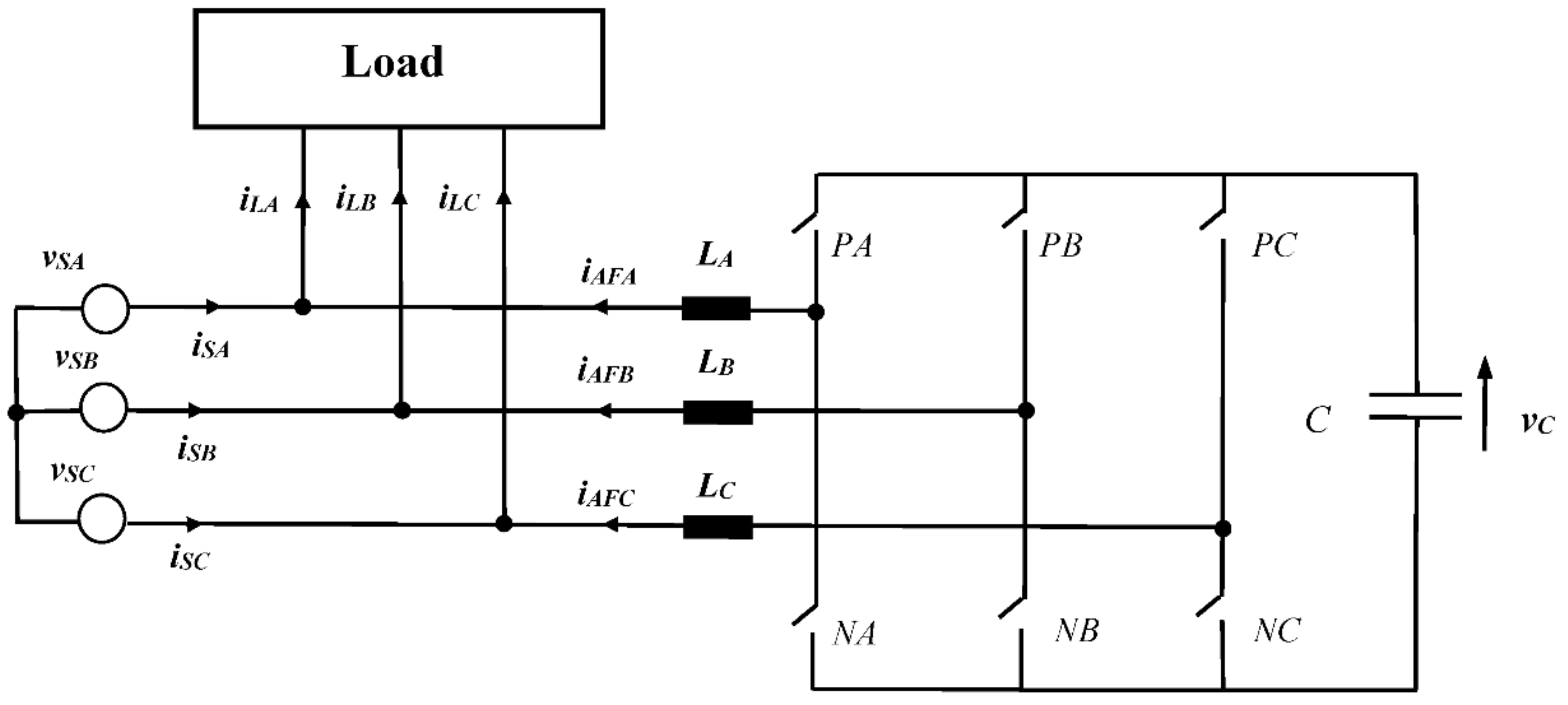
The circuit shown in Figure 2 includes a three-phase power source vSA, vSB, and vSC; a load and the power processing module of the active filter. This module consists of smoothing inductors LA, LB, and LC; then six power switches PA, PB, PC, NA, NB, and NC, which shape the active filter current.

2.2. Load Equivalent Conductance Signal—Direct Control Technique Approach

The signal gD of the load equivalent conductance can be based on load phase instantaneous voltages and currents. According to the Fryze–Buchholz–Depenbrock theory [45], this signal is:
g D = k v k i k k v k 2
where k is phase index, vk is instantaneous phase voltage and ik is instantaneous load phase current.
The numerator of the right-hand size fraction in (1) is related to the load instantaneous power and the denominator can be considered as the instantaneous norm of the source voltage. All phase voltages and currents have to be sensed to calculate the conductance signal (1).
On the base of (1) Depenbrock power currents were introduced:
i p , k = g D v k
The currents (2) carry the active power of the load only, i.e., they do not deliver the energy related to the loss of energy in the active filter circuitry. However, this loss must not be neglected. An additional circuit is often used to measure the power of this loss and to add it to the total source loading. Finally, this summed active power loads the source. After such conductance signal complementation, the references for supply source phase currents may be defined as follows:
i S , k * = ( g L + g A F ) v k
where i* denotes current reference signal.
If the source phase currents are controlled in closed-loop in accordance with Equation (3), the compensating currents, namely, phase currents of the active filter, are not computed at all. The active filter generates them “automatically” in some measure, and their waveforms can be explained on the base of the Kirchhoff’s Current Law. These currents can be related to Depenbrock “powerless currents”. They satisfy the equation:
i n , k = i k i p , k
and do not contribute to the load active power.

3. Inertial Indirect Method of Current Reference Determination

3.1. Overall Form of the Equivalent Conductance Signal

To obtain reference signals (3), which consists of equivalent conductance of the load and the active filter, an analysis of energy changes occurring in the source—active filter—load circuit was carried out. The following assumptions were made regarding the operation of the system:
(1)
Each change in magnitude of the load active power PL, and/or in energy loss PAF in the active filter circuitry, is transformed into the adequate change of magnitude of the conductance signal.
(2)
After each change of the load active power, and/or change of energy loss in the active filter circuitry, the conductance signal aims the steady state exponentially with a user-defined time Tst.
A zero-to-PL step-change of the load active power may be applied to obtain the total equivalent conductance signal, i.e., the signal that is related to the PL and PAF powers, compare (3).
Let the active filter be already on when the power PL appears at time t = 0. Accordingly to Fryze [45,46] the total load and active filter equivalent conductance may be introduced:
G = P L + P A F V S Σ 2
where V S Σ 2 is Buchholz’s equivalent voltage of polyphase source.
According to the assumptions (1) and (2) the equivalent conductance signal can be defined as:
g ( t ) = G 1 e t N τ T s t
The source, active filter and load currents aim the steady state satisfying the following relationships: source phase currents:
i S , k ( t = 0 ) = 0
i S , k ( 0 < t T s t ) = G 1 e t N τ T s t v k
i S , k ( t > T s t ) = G v k
active filter phase currents:
i A F , k ( t = 0 ) = G v k
i A F , k ( 0 < t T s t ) = G v k e t N τ T s t
i A F , k ( t > T s t ) = 0
load phase currents:
i L , k = i S , k + i A F , k = G v k
where: iS,k, iAF,k, and iL,k are source phase currents, active filter phase currents, and load phase currents, respectively; PAF is power dissipated (loss) in the active filter circuitry; Nτ is a user-defined number of time constants τ after which the steady state can be considered to be reached: Nτ = Tst/τ
Now, accordingly to the assumptions (1) and (2) and to the relationships (6)–(13), the basic equation for the total energy balance (i.e., between the load, the active filter, and the supply source) can be formulated:
( P L + P A F ) t = ( W A F i n i w A F ( t ) ) + k 0 t v k i S , k d τ
where: WAFini is amount of energy stored initially (i.e., during the active filter initialization procedure) in the active filter reactance elements; wAF(t) is amount of energy stored in these elements at instant t.
Equation (14) describes that changes in the active power of the load and/or energy loss in active filter cause a transient during which these changes are balanced by two streams of energy simultaneously: a stream supplied by the active filter and a stream supplied by the supply source.
With a slight simplification it can be assumed that just after the load power is changed it is balanced by the active filter solely. Over time, the power delivered from the active filter decreases until reaching the steady state: here the state, when the load is supplied from the supply source entirely.
To describe the energy relation between the source and the active filter until reaching the steady state, a parameter NSF (source-to-filter amount of energy ratio) may be defined:
N S F = W S [ 0 , T s t ] Δ W A F [ 0 , T s t ] = k 0 T s t v k i S , k d τ W A F i n i w A F ( T s t )
Taking into account that after change of the load active power the envelopes of source current and the active filer current change exponentially, the parameter NSF can be written with the use of the coefficient Nτ as follows:
N S F = N τ 1 e N τ 1
Once the parameter NSF has been introduced, Equation (14) can be expressed as a function of the active filter energy change solely:
( P L + P A F ) T s t = Δ W A F + W S = Δ W A F + Δ W A F N S F = Δ W A F N S F + 1
The overall equation for the equivalent conductance signal can be formulated by dividing (17) by the term T s t V S Σ 2 :
g ( t ) = W A F i n i w A F ( t ) N S F + 1 T s t V S Σ 2
The conductance signal (18) is obtained on the base of information on amount of energy stored in the active filter exclusively. There are two legs to this statement: the stream of energy flowing between the supply source and the load is identified via the amount of energy stored in the active filter, and the second leg, without any assumptions about the type of the system structure in which the active filter works. Therefore, Equation (18) is universal in the sense that it can be applied for active filters working in the DC as well as in the AC systems, i.e., without any constraints on the structure of the system: for a single- or polyphase circuits, and for voltage- or current-inverter (VSI or CSI, respectively)-based active filters.

3.2. Energy Circulation in the Source-Active Filter-Load Circuitry

For the sake of clarity of the argument, the energy circulation in a circuit with an active filter can be analyzed in two aspects: buffering of load active power changes and managing of in-load generated power. However, these two phenomena can impact each other to some extent.

3.2.1. Buffering of Load Active Power Changes

Due to the “implemented inertia” in the operation of the active filter (6), each change in the load active power is seen by the source with some delay (8). By selecting the time Tst it is possible to define this inertia, which is connected with the mutual relation of energies taken from the source and from the active filter, (14). The longer the time Tst, i.e., the time to reach the steady state in the circuit, (8), the higher level of energy buffering. This phenomenon can be an advantageous feature of the discussed method. The energy buffering allows averaging the source power and lowering energy loss in the supply line in a case of variable load.

3.2.2. Managing of In-Load Generated Power

The conductance (18) may go negative if the energy wAF(t), which is actually stored in the active filter, oversteps the energy WAF0 that has been stored in the active filter during its starting up. Such phenomenon may appear if load becomes generative (i.e., generating power in a considered period of time). In general, transitions of the conductance (5) and conductance signal (18) from positive to negative sign, and vice versa, is associated with the consumption or generation of energy in devices connected to the active filter. It does not matter whether they are connected on the AC or DC side of the filter. The energy flow between all these devices can be averaged, or buffered, by selecting the magnitude of the Tst factor.

3.3. Equivalent Conductance Signal for the Voltage-Source Inverter Based Active Filter

The active filter may be based on a voltage source inverter. In such a case, the active filter energy is stored mainly in its DC-link capacitor and, in a small part, in its AC-side smoothing reactors. Therefore, Equation (18) can be rewritten in the form exposing the amount of energy stored in these reactance elements:
g ( t ) = K V V D C i n i 2 v D C 2 ( t ) + k K I , k I A F i n i , k 2 i A F , k 2 ( t )
where:
K V = C N S F + 1 2 T s t V S Σ 2
K I , k = L k N S F + 1 2 T s t V S Σ 2
and where: IAFini,k and iAF,k(t) are active filter phase currents at the moment on turning the load on, and at instant t, respectively; C is capacity of active filter DC-link capacitor; Lk are inductances of active filter’s AC-side smoothing inductors.
The constants KV and KI,k give proportions to energy-to-conductance signal relations and can be used as gain coefficients of P-type regulators, which may be elements of the active filter signal processing module.

4. Current References Based on Continuous or Step Conductance Signal

4.1. Continuous Conductance Signal

As long as the source and load voltages and currents are sinusoidal and balanced, the conductance signal (1) remains constant. Consequently, the reference currents (3) are sinusoidal and in-phase with the corresponding phase voltages. After compensation for reactive power in such a system, the source currents are optimal and carry pure active power with unity power factor. Such circumstances no longer exist if the system changes to unbalanced or non-sinusoidal or transient conditions. The reference signals (3) may be distorted even in such a situation, when the source phase voltages are sinusoidal and the load is purely resistive but unbalanced.
Figure 3 shows representative waveforms of an unbalanced three-phase circuit considered from the perspective of the FBD theory. The source phase voltages are balanced, each with 100 V rms. The load is resistive, consisting of three resistors in Y configuration, Ra = Rb = 10 Ω and Rc = 100 Ω. Load phase currents are sinusoidal with rms equal 8.7 A, 8.7 A and 1.4 A for phases A, B and C, respectively. The Buchholz’s norm of load currents is 12.4 A. The conductance signal gD is presented in compliance with (1), and then Depenbrock’s phase power currents in compliance with (2).
If the Depenbrock power currents were to be used as reference signals for the source phase currents then the improvement in power factor would be achieved to some extent. Indeed, as a result of such compensation load phase currents align slightly, reaching rms of 7.4 A, 7.4 A, and 4.2 A for phases A, B, and C, respectively. Resultantly, the Buchholz norm of these currents diminishes to 11.3 A. However, at the same time the third-order harmonic appears in the current reference signals. Consequently, the source currents become distorted, remaining unbalanced. The cause of these unfavorable phenomena is the oscillating component in the conductance signal (1). Therefore, there is still a large space to improve the compensation quality.

4.2. Step Conductance Signal

For the sinusoidal but unbalanced load the unity power factor can be reached by elimination of the oscillating component from the conductance signal gD (1). This can be done by processing the signal (1) to be invariable (constant in time) within each subsequent period Tm. This approach is appropriate as well for the direct as for the indirect control method, where the conductance signal is defined by (19).
The second problem to be considered is the moment of obtaining the necessary magnitude of the conductance signal. From the definitions of active power and rms of voltage/current signal result that one period T is needed to calculate both quantities. Therefore, the conductance signal (19) seems to be useless as being known “too late” from the perspective of the ongoing period Tm. This problem can be solved by sampling magnitude (19) periodically, at the very end of each period Tm, and then applying each sample for the next Tm+1 one. Such an approach requires buffering the energy flow between the source and the load. Notice, it is coherent with the method of obtaining the conductance signal (18).
Let the time Tst be equal to the period T. The first period T1 of the active filter action is crucial, therefore it should be analyzed carefully. It is obvious that in this period there is no information on previous power dissipation, which could be “memorized” in active filter reactance elements, see (5) and (18). For that reason, the initial magnitude of the conductance G, i.e., during the time when the active filter is already ready to be used but before it starts compensation, it has to be zero. As a result, during the first period T1 the reference for source currents are null. Consequently, during this T1 period the supply source currents cannot flow and, therefore, the load can be supplied solely using energy stored in the active filter. After the period T1 is ended the conductance G is already known. It can be applied for the next period T2. To perform such a supply-shift by one period T, the active filter DC-side capacitor has to be initially charged to the proper voltage and energy, (18), (19).
Assuming that the steady state is to be reached after one period T, the NSF should be zero (15). This is due to the fact that within this period T all the energy consumed in the source–active filter–load circuit is taken from the active filter reactance elements solely.
The reasoning presented for the period T1 and T2 can be extended to each power change PL and PAF occurring in any period Tm and impacting the next period Tm+1. Therefore, the conductance signal and then the source reference currents can take the final form exposing “the shift” of the conductance signal by one period T:
G T m = K V V D C i n i 2 v D C 2 ( T m 1 ) + k K I , k I A F i n i , k 2 i A F , k 2 ( T m 1 )
i S , k , T m * = G T m v k
where m is index of ongoing T period.
During the operation of the active filter, the voltage of the DC-link capacitor changes due to compensation for the nonactive current and due to buffering of variations of load active power. In order to have control over the source current, this voltage must always be greater than the peak of the supply source line-to-line voltage, practically at least by 50%.
On the other hand, the upper voltage limit of this capacitor must be also considered. Both the parameters of the switches, which operate in the power processing module of the active filter, and the type of load, with which the filter works, should be taken into account. In particular, depending on the type of load, this upper limit may be the initial voltage VDCini, in the case of a passive load, or a higher voltage, if the load can go into active (generative) mode of operation. The case of active filter cooperation with an active load is introduced in Section 5.1 and is also analyzed in the following sections.
The required capacitance of the DC-link capacitor can be estimated as follows. Assuming that Gmax is the largest magnitude of the equivalent conductance signal, which is possible in the considered circuit, and that the DC-link capacitor voltage cannot decrease below a certain minimum magnitude VDCmin, the required capacity of the DC-link capacitor can be obtained from Equation (22)—while taking into account Equations (20) and (21).
C = 2 T V S Σ 2 G max k L k I A F i n i , k 2 i A F , k 2 ( T 1 ) V D C i n i 2 V D C min 2
The voltages entered in the denominator of Equation (24) may be selected to provide a voltage range convenient from the point of view of its measurement and processing for the computation of the conductance signal, compare (22).
The energy stored in the Lk chokes of the active filter are insignificant in relation to the energy stored in the DC-link capacitor. For this reason, the second component in Equation (24) may be omitted.

4.3. Conductance Signal for Three-Phase Four-Wire Active Filter

The active filter controlled by the conductance signal can also work in a three-phase four-wire circuit. Active filter structures with one [47], or two capacitors [24,48,49,50,51,52,53] are possible. A dual-capacitor system is considered below to show the possibility of controlling the active filter with the use of the conductance signal also in the case of the dual-capacitor structure.
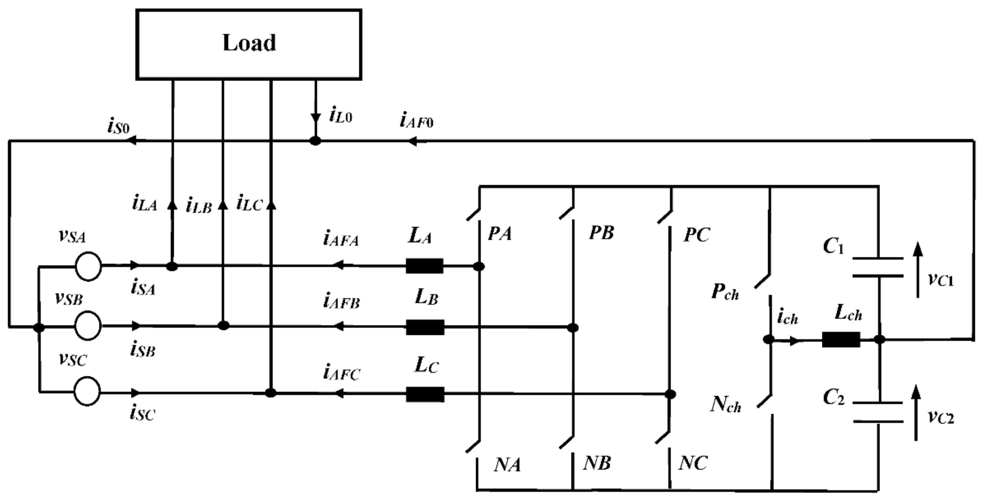
The circuit shown in Figure 4 includes a three-phase power source vSA, vSB, and vSC; a load and the power processing module of the active filter. This module consists of smoothing inductors LA, LB, and LC; six power switches PA, PB, PC, NA, NB, and NC, which shape the active filter current; and two capacitors C1 and C2 that constitute the energy storage of the active filter. Additionally, the power processing module includes a subcircuit—which contains two switches Pch and Nch, and inductor Lch—for balancing the voltages of the capacitors C1 and C2. This subcircuit is activated when a current constant component in the load neutral conductor appears.
As shown in the previous sections, the change in load active power causes a static change in the energy stored in the reactance elements of the active filter. In the case discussed here, this change in energy affects both capacitors constituting active filter’s DC-link circuitry, and four inductors: LA, LB, LC, and Lch. The total energy change in all listed reactance elements is the sum of the separate energy changes in all individual elements:
Δ W T m = C 1 v C 1 2 T m v C 1 2 T m 1 2 + C 2 v C 2 2 T m v C 2 2 T m 1 2 + k K I , k i A F , k 2 T m i A F , k 2 T m 1
where: vCx(Tm) is C1 or C2 capacitor voltage at the end of period Tm; vCx(Tm−1) is C1 or C2 capacitor voltage at the end of period Tm−1.
The energy changes of the reactance elements add up in the successive periods T. As a result, the equivalent conductance signal for any period Tm can be calculated as follows:
G T m = K V 1 V D C 1 i n i 2 v D C 1 2 T m 1 + K V 2 V D C 2 i n i 2 v D C 2 2 T m 1 + k K I , k I A F i n i , k 2 i A F , k 2 T m 1
where:
K V 1 = C 1 2 T s t V S Σ 2   and   K V 2 = C 2 2 T s t V S Σ 2

5. Verification of the Conductance Signal Control Method

The presented control method has been verified by means of computer simulation. The IsSpice software (Intusoft, San Pedro, CA, USA, [54]) has been used.
A series of simulation experiments were carried out to investigate the considered control method. The three-wire system, shown in Figure 2, is considered. The possibility of compensating for highly distorted currents, often to an extent practically not found in electrical circuits, was investigated. This approach can be seen as a worst-case study.

5.1. Basic Properties of the Filter Control Using the Conductance Signal

The purpose of the analysis carried out in this section is to verify the general correctness of the presented control method.
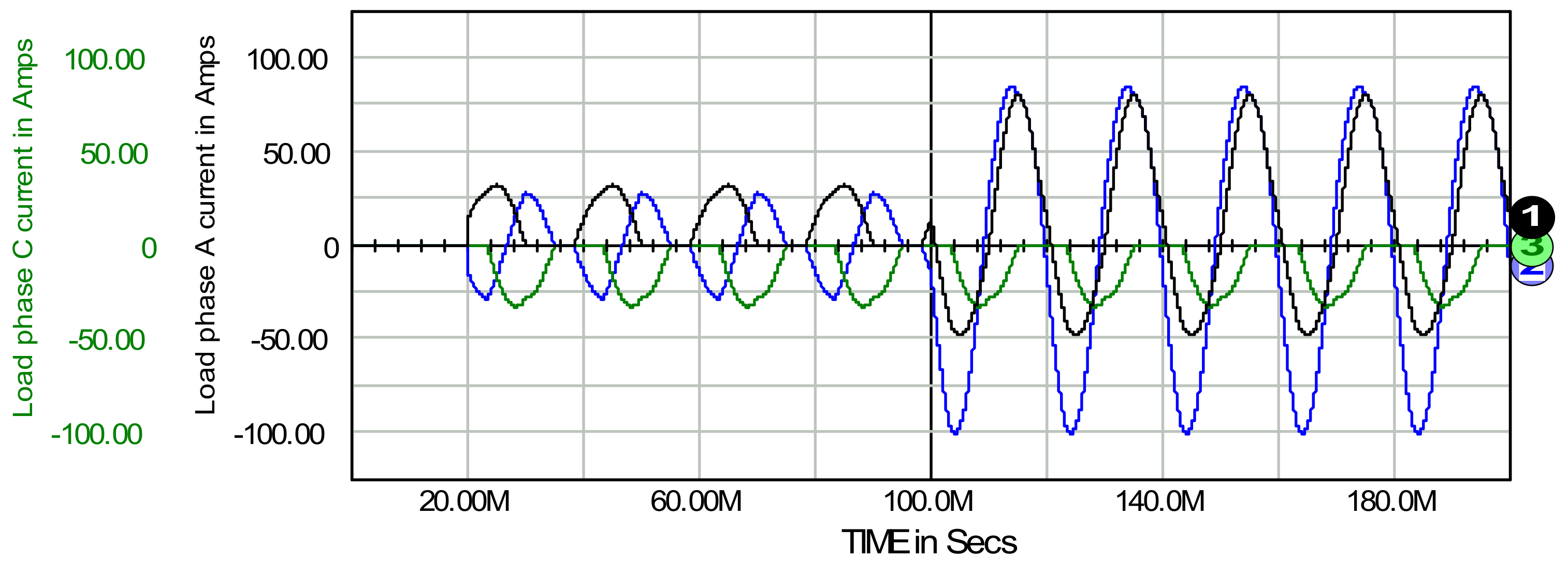
The applied load, which nonactive currents are to be compensated, consists of a passive part and an active (generative) part. The passive part consists of a series connection of a 9 Ω resistor and a diode in phase A and in phase C, and a single 9 Ω resistor in phase B. These three load branches work in connection Y. The passive part of the load is activated at time t1 = 20 ms.
The load active part is a single-phase generator, which is connected asymmetrically to the line-to-line voltage VAB. It generates a sinusoidal current, which is reversed to the source phase voltage VA, vSA in Figure 2, with an amplitude of 80 A and of frequency of 50 Hz. The generative part of the load is activated at time t2 = 100 ms.
Phase current waveforms of the load are shown in Figure 5. The Tst parameter (defining the time to reach the steady state, (18)–(21)), is set to be equal to the period T.
On the base of Figure 5 the mean, rms and THD parameters of load phase currents (iLA, iLB and iLC in Figure 2) are as follows:
  • Time period 20 ms–100 ms:
    • phase A: 12.2 A mean, 17.6 A rms and 29% THD
    • phase B: 0.0 A mean, 17.3 A rms and 37% THD
    • phase C: −12.3 A mean, 17.7 A rms and 29% THD
  • Time period 100 ms–200 ms:
    • phase A: 12.2 A mean, 46.5 A rms and 29% THD
    • phase B: 0.0 A mean, 66.5 A rms and 37% THD
    • phase C: −12.2 A mean, 17.6 A rms and 29% THD
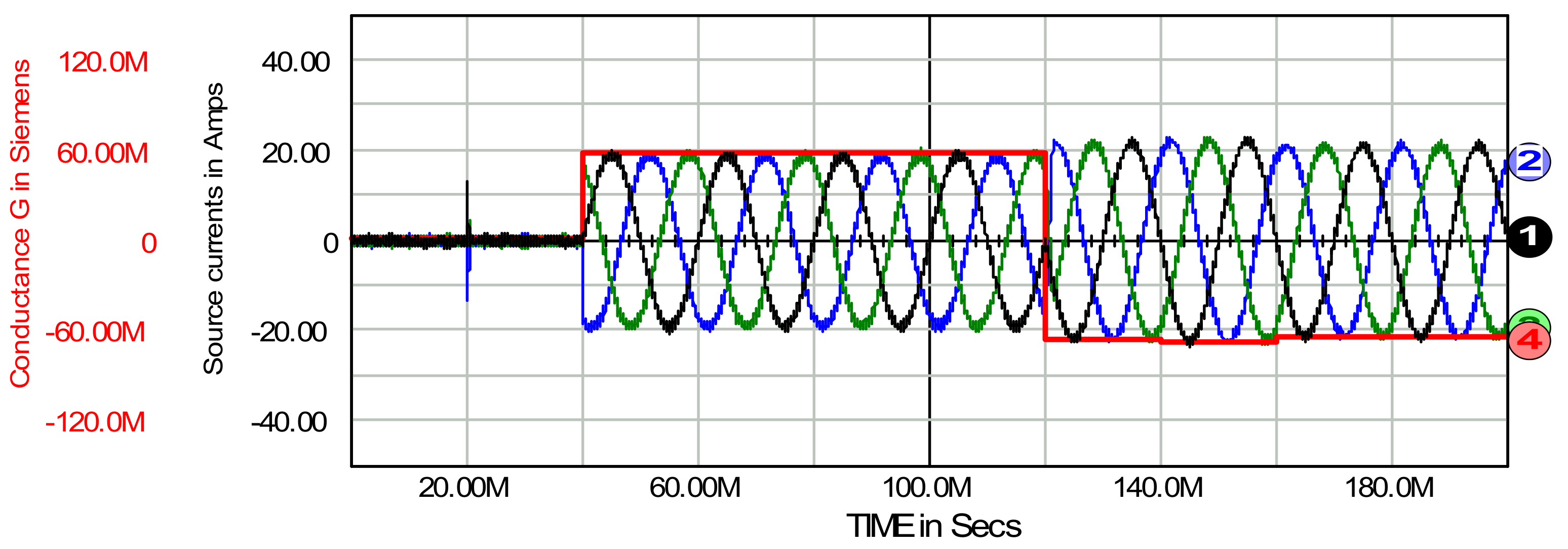
Source phase currents (i.e., compensated currents, iSA, iSB, and iSC in Figure 2) and the conductance signal (22), are presented in Figure 6. The passive part of the load is switched on at t1 = 20 ms, and the generative part is activated at t2 = 100 ms.
On the base of Figure 6 the mean, rms and THD parameters of source phase currents are as follows:
  • Time period 40 ms–120 ms:
    • phase A: −0.06 A mean, 13.4 A rms and 1.4% THD
    • phase B: −0.03 A mean, 13.5 A rms and 1.9% THD
    • phase C: 0.09 A mean, 13.5 A rms and 1.9% THD
  • Time period 120 ms–200 ms:
    • phase A: −0.02 A mean, 14.9 A rms and 1.4% THD
    • phase B: 0.02 A mean, 14.9 A rms and 1.5% THD
    • phase C: −0.02 A mean, 14.8 A rms and 1.2% THD
The comparison of the load current and source current parameters shows that the correctness of the global compensation has been obtained for the following reasons:
  • source phase currents are practically sinusoidal waveforms of fundamental frequency,
  • they are in phase with waveforms of respective phase voltages, and
  • they are symmetrical.
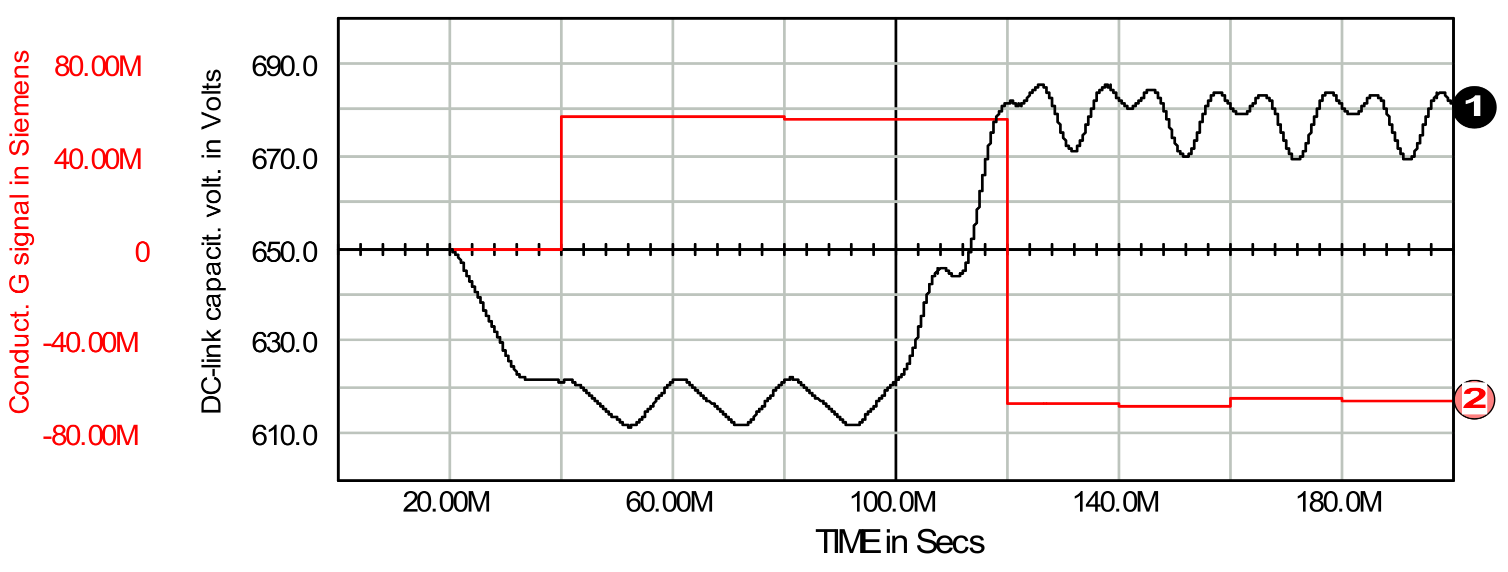
Some specific features of compensation with the use of the conductance signal may be emphasized. To do this, the DC-link capacitor voltage (vC signal in Figure 2) and then the conductance signal, obtained on the base of this voltage according to (22), are presented in Figure 7, and then analysed and concluded.
Based on Figure 7, some characteristic parameters of both signals can be read:
  • Time period 40 ms–100 ms: G: mean 56.97 ms, st. dev. 0.22 ms; DC-link volt.: mean 617.0 V, pk-pk: 10.3 V
  • Time period 120 ms–200 ms: G: mean −66.12 ms, st. dev. 1.37 ms; DC-link volt.: mean 679.8 V, pk-pk: 14.8 V
On the basis of these parameters it can be concluded that:
  • energy changes in load active power are buffered by active filter;
  • as assumed, the steady state is reached in one period T of supply source cycle after each change of load active power;
  • in the steady state the conductance signal is practically constant and its mean indicates the actual magnitude of sum of load and active filter active powers: 9.1 kW (positive, consumed) and, simultaneously, −10.5 kW (negative, generated) for time periods 40 ms–100 ms and then 120 ms–200 ms, respectively;
  • energy flow is bidirectional and is in clear relation to the DC-link capacitor voltage (with respect to its initial voltage VDCini, comp. (19) and (22));
  • there is an excess of the active power generated in the generative part of the load in relation to the consumed active power in the load-and-active filter circuitry. The difference of both powers is transmitted to the supply source with unity power factor—in a balanced manner.

6. Transmit, Store, and Inertial Mode of Active Filter Operation

The energy upstream transmission, as a natural consequence of increasing the voltage on the DC-link capacitor above the initial magnitude, was introduced in Section 5.1. Such a transmission may appear if some amount of energy, which exceeds the energy consumed, is generated in the load. This regime of active filter activity is named here the transmit mode of operation. However, there is the possibility of storing the energy generated in the load as an option to the energy transmission. This regime of active filter activity can be named the store mode of operation.
Regardless of these two operating modes, it is possible to increase the inertia of the filter response to changes in load active power. In this way, it is possible to average the power of the source in the case of a time variable load. These topics are discussed sequentially in this section.
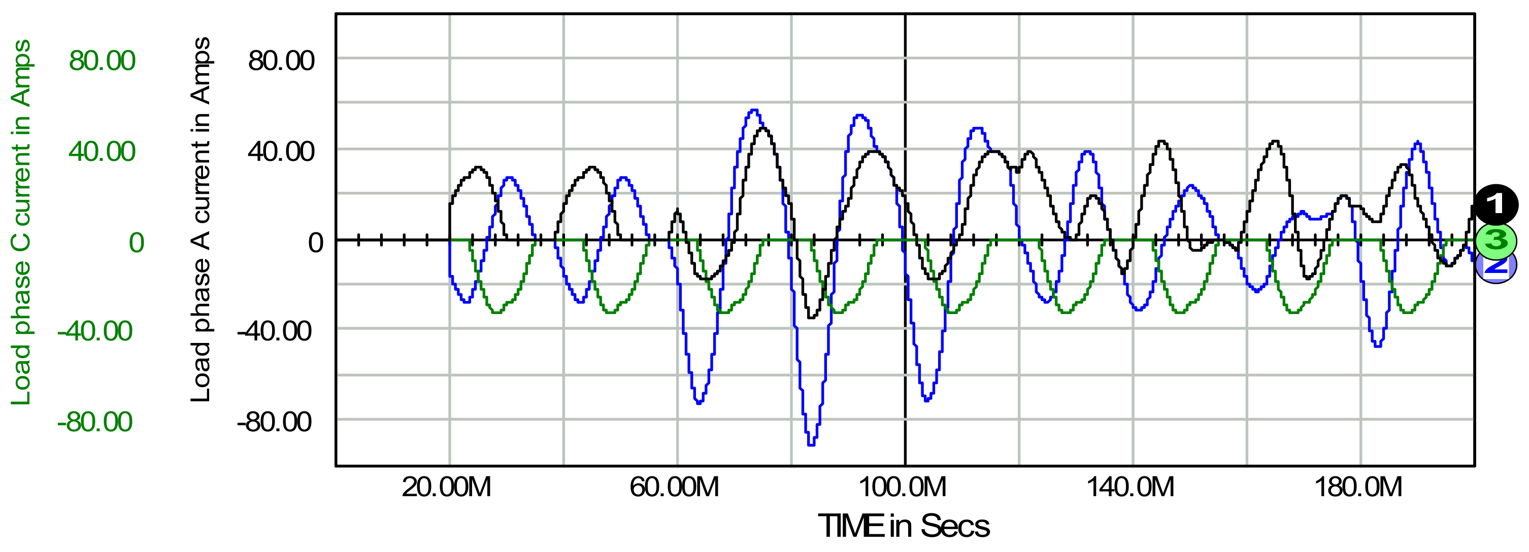
In this section a more distorted load current is introduced to test the active filter performance. Except for Section 6.3, it is common for all simulations in this section. In particular, two current interharmonics, one of 70 Hz frequency and another of 90 Hz frequency, both of 10 A in amplitude, have been added to the generative part of the load (compare Figure 5 and Figure 8). The active (generative) part of the load is activated at the time instant ton = 60 ms and turned off at toff = 120 ms.
The mean and rms parameters of load phase currents, for the time period 20 ms–180 ms, are as follows: phase A: 12.2 A mean and 22.4 A rms; phase B: 0.0 A mean and 31.9 A rms; and phase C: −12.2 A mean and 17.6 A rms. Buchholz norm for these currents is 42.8 A.

6.1. Transmit Mode of Active Filter Operation

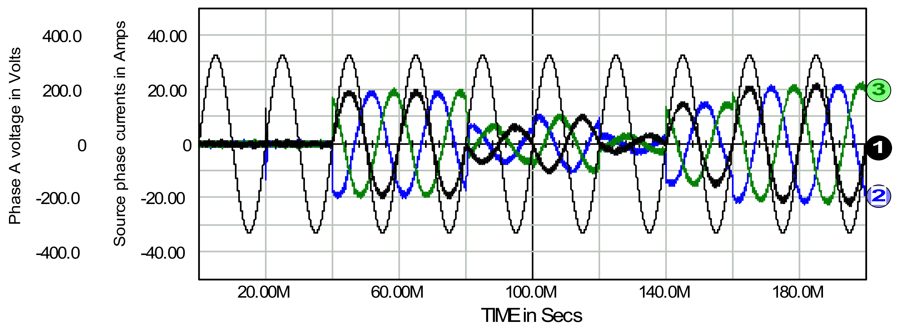
The result of compensation with the use of the transmit mode is presented in Figure 9.
The mean and rms parameters of source phase currents, calculated for the time period 40 ms–200 ms, are (source phase currents are symmetrical): 0.0 A mean and 11.2 A rms.
In particular:
  • 13.5 A in time period 40 ms–80 ms (energy consumption),
  • 4.5 A in 80 ms–100 ms (energy generation),
  • 7.0 A (generation) in 100 ms–120 ms,
  • 2.1 A (generation) in 120 ms–140 ms,
  • 10.4 A (consumption) in 140 ms–160 ms,
  • 15.1 A (consumption) in 160 ms–200 ms
Buchholz norm of source phase currents, for time period 40 ms–200 ms, is 11.2 A.
In particular:
  • 23.4 A in 40 ms–80 ms,
  • 7.8 A in 80 ms–100 ms,
  • 12.1 A in 100 ms–120 ms,
  • 3.6 A in 120 ms–140 ms,
  • 18.0 A in 140 ms–160 ms,
  • 26.2 A in 160 ms–200 ms
It can be concluded that source current is free from nonactive components, so its magnitude—in terms of the “multiperiod” Buchholz equivalence—has been reduced.
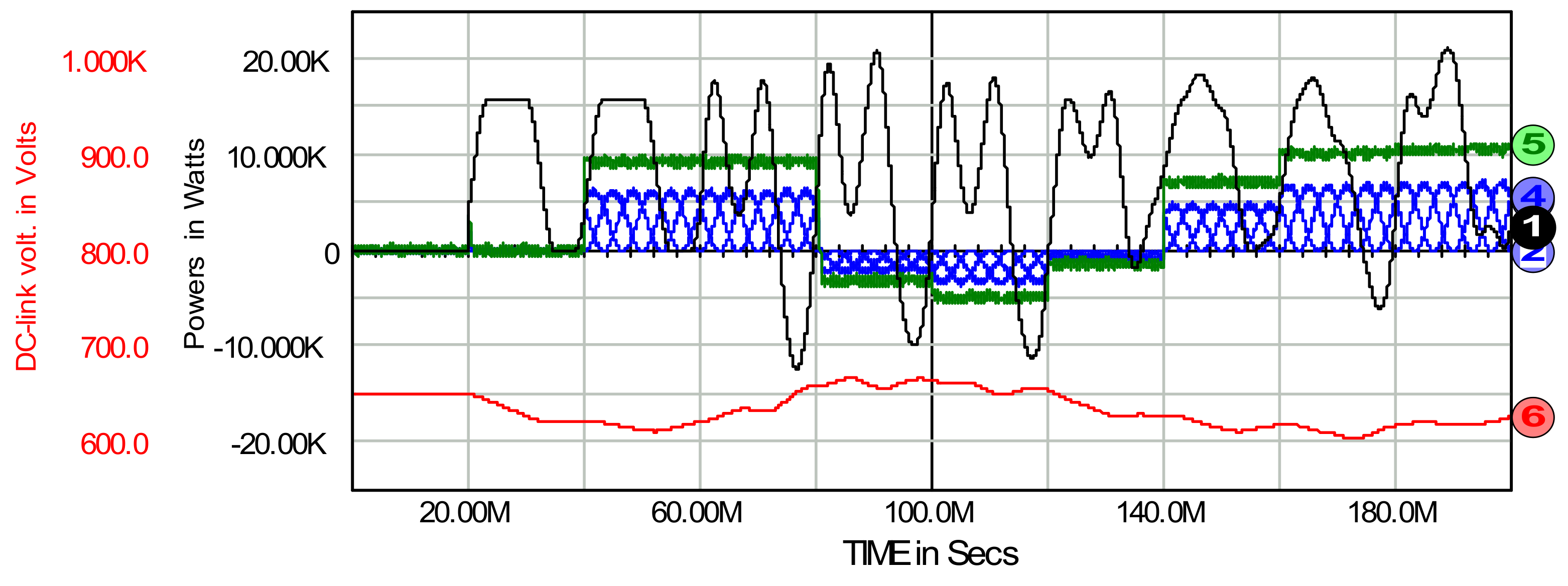
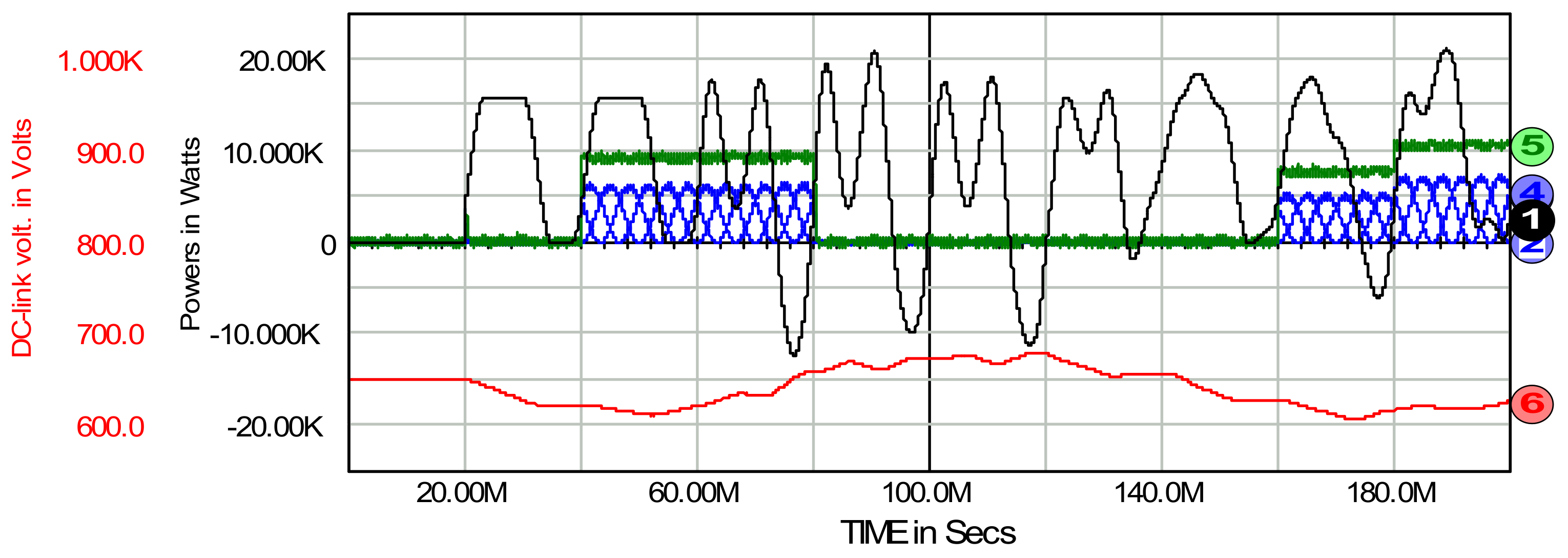
As the conductance signal depends on the energy flow in the circuit, Figure 10 shows the operation of the circuit once again, but this time in terms of power.
It can be said that distorted and unbalanced load power, waveform 1 in Figure 10, has been transferred into “linear” and balanced one. This power quality improvement was achieved by buffering the energy flow in the circuit, as a result of the operation of the DC-link capacitor, waveform 6. However, the source power is still time variable from one period T to another, waveforms 2–5.

6.2. Store Mode of Active Filter Operation

The energy flow in the circuit is bidirectional, Figure 9 and Figure 10, which may be considered disadvantageous. Fortunately, there is the possibility of storing the “excessive” amount of the in-load generated energy in the active filter’s DC-link capacitor. This energy can be then consumed in the passive part of the load. As the result the supply source can be relieved from the doubled transmission of this amount of energy. Figure 11 and Figure 12 illustrate this possibility.
The mean and rms parameters of source phase current, calculated for the period 40 ms–200 ms, are (source phase currents are symmetrical): 0.0 A mean and 9.5 A rms.
In particular:
  • 13.5 A in 40 ms–80 ms,
  • 11.2 A in 160 ms–180 ms,
  • 15.5 A in 180 ms–200 ms
Buchholz norm of rms magnitudes of these currents for the time period 40 ms–200 ms is 16.5 A.
In particular:
  • 23.3 A in 40 ms–80 ms,
  • 19.6 A in 160 ms–180 ms,
  • 26.5 A in 180 ms–200 ms
Figure 12 exemplifies the circuit operation shown in Figure 11 again, now in terms of power and energy. The load acts analogous to the previous example and its currents are of the same shape as shown in Figure 8.
The instantaneous power of the load, waveform 1 in Figure 12, is “nonlinear” and partially negative (i.e., of generative or active type). As a result of compensation and accumulation in the DC-link capacitor of the excess energy generated over the consumed in the load, the source power is “linear”, “balanced”, and permanently non-negative. The source active power is 9.3 kW in the time period 40 ms–80 ms, then 7.7 kW in the time period 160 ms–180 ms and 10.6 kW in the time period 180 ms–200 ms. The related magnitudes of conductance signal (5) are 56.8 ms, then 47.2 ms and 65.3 ms, respectively.
During the time period 80 ms–140 ms the conductance signal (5) should be negative, see waveform 6 in Figure 12 and Equation (22). However, in order to prevent energy flow upstream to the supply source, the negative magnitude of the conductance signal is limited to zero here.

6.3. Inertial Mode of Active Filter Operation

Regardless of transmit or store mode of active filter operation the inertial mode of operation may be introduced. The introduction of this mode consists in increasing the parameter (the time period) Tst. The inertial mode in combination with the transmit mode of active filter operation is considered in this section.
The load parameters are similar to those defined in Section 5.1. The only difference consists in increasing load resistors from 9 Ω to 12 Ω in order to lower active power of the load passive part. The load active (generative) part remained unchanged and is turned on at time instant ton = 60 ms and turned off at toff = 320 ms.
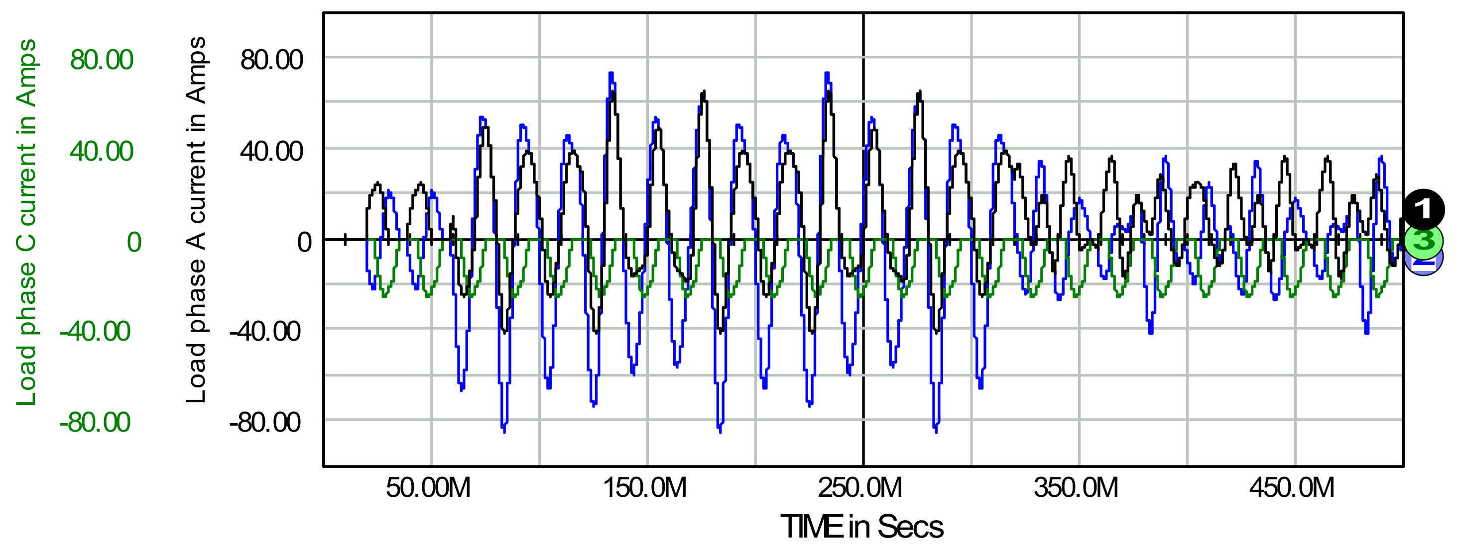
The load phase currents are shown in Figure 13. Their mean and rms parameters for the time period 20 ms–480 ms are: phase A: 9.4 A mean and 24.5 A rms; phase B: 0.0 A mean and 34.8 A rms; phase C: −9.4 A mean and 13.6 A rms. The “multiperiod” Buchholz norm of these currents is 44.7 A.
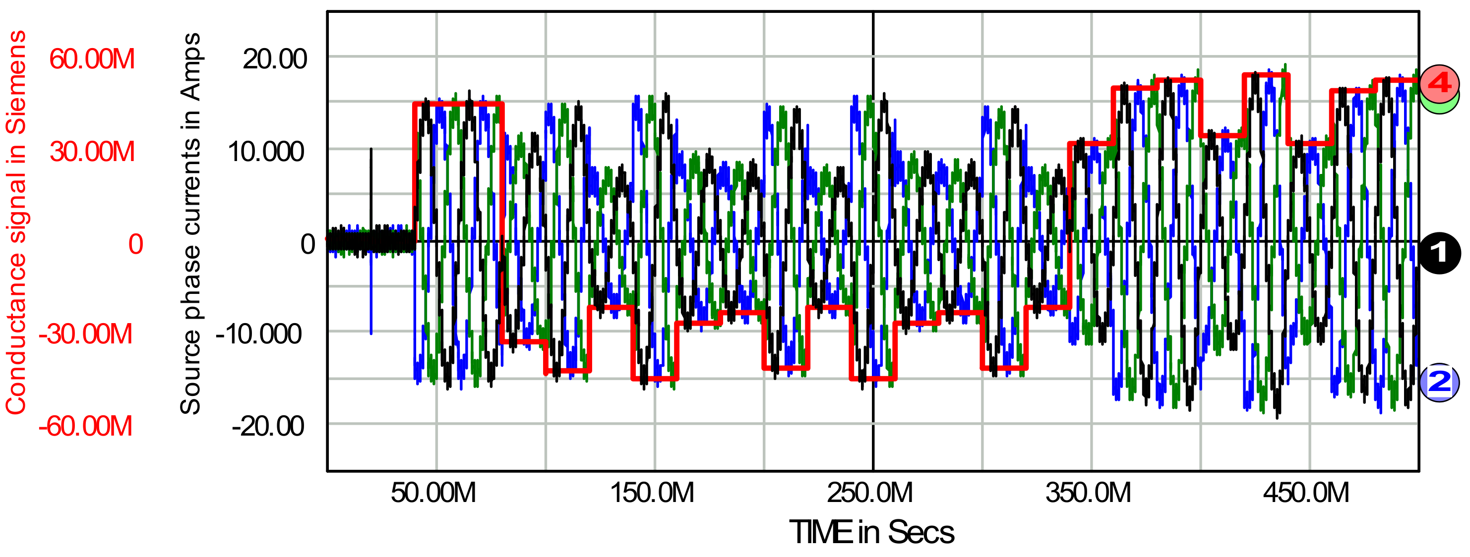
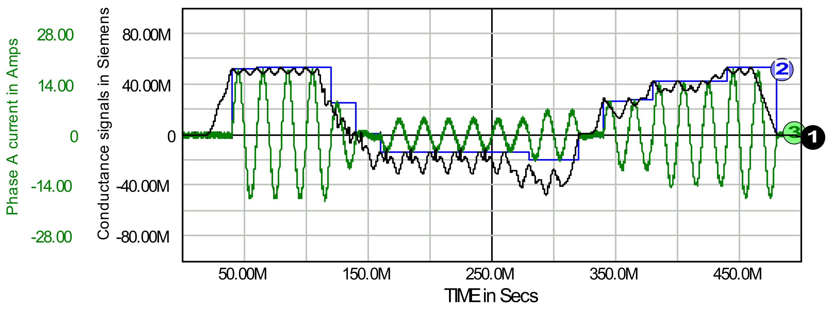
The source phase currents and the conductance signal are shown in Figure 14. The active filter acts in transmit mode and with no inertia yet. In such configuration the steady state is reached in one period T after each change of load active power and the excessive in-load generated active power is transmitted upstream to the source. This operating configuration is confirmed by the conductance signal waveform shown.
The mean and rms parameters of source phase currents for phase A, B, C, and for time period 40 ms–500 ms are (source phase currents are symmetrical): 0.0 A mean and 9.1 A rms. Buchholz norm of rms magnitudes of these currents for the same time period is 15.7 A. Standard deviation for the conductance signal is 38.9 ms. Comparing parameters of load and source current it can be stated that nonactive currents have been compensated, so that the power quality has been significantly improved.
However, observing the waveforms shown in Figure 14 it can be noticed that the high variability of the load power is still “transferred” to large variability, from one period T to another, of the source power. Fortunately, this source power variability can be reduced if the inertial filter mode of operation is used.
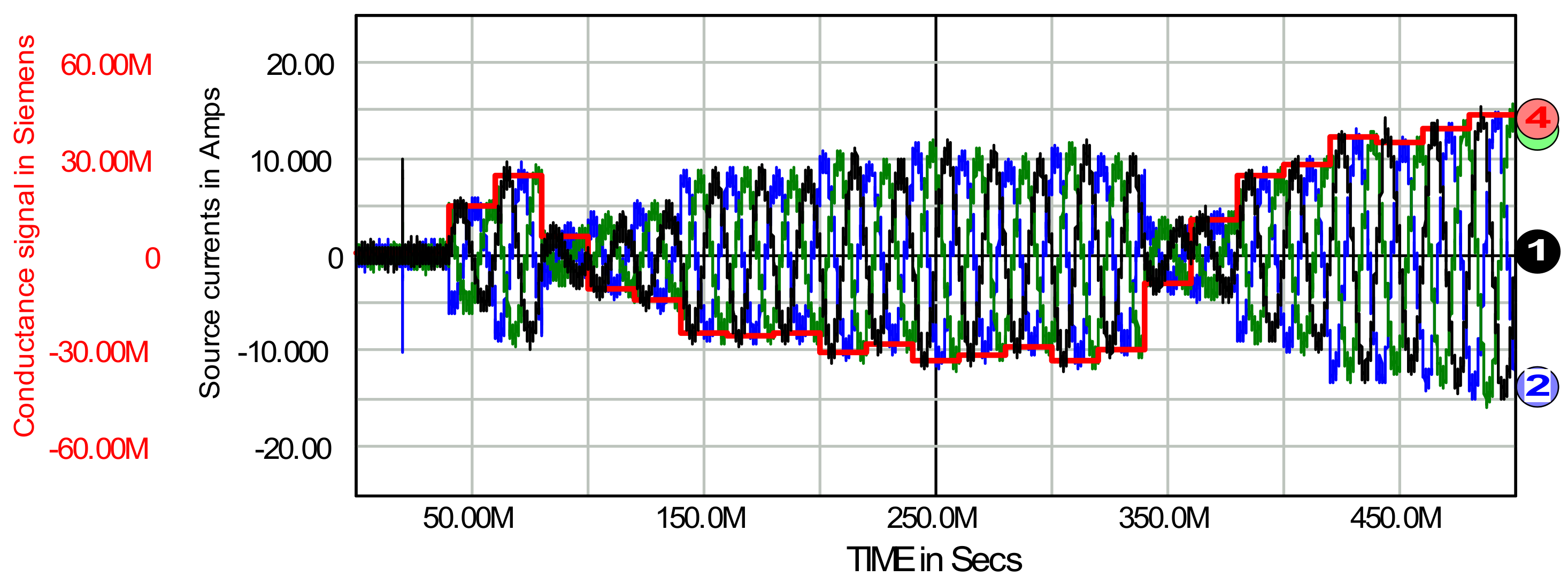
The inertial mode of the active filter operation is now introduced by the triple increase in the value of the Tst parameter. After this change the new source phase currents and conductance signal waveforms are shown in Figure 15. Noticeable, the conductance signal tends each new steady state step-by-step, or, using other words, in an inertial manner.
For the analyzed transmit-and-inertial mode of operation the mean and rms parameters of source phase current for phase A, B, and C for time period 40 ms–500 ms are 0.0 A and 6.4 A, respectively. Buchholz norm of rms magnitudes of these currents for the same time period is 11.1 A. Standard deviation for the conductance signal is 27.2 ms. A comparison of these values with the previous ones, with no inertia in active filter action, confirms a significant reduction in the charge of the power source.
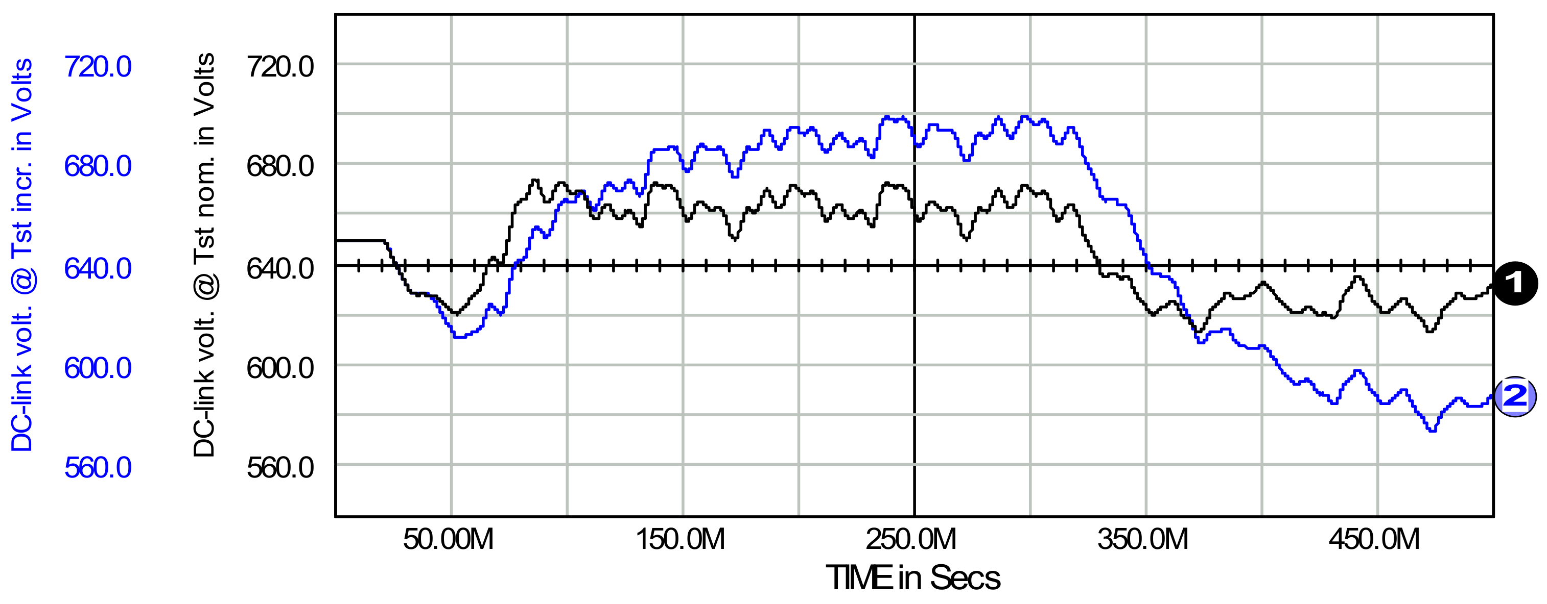
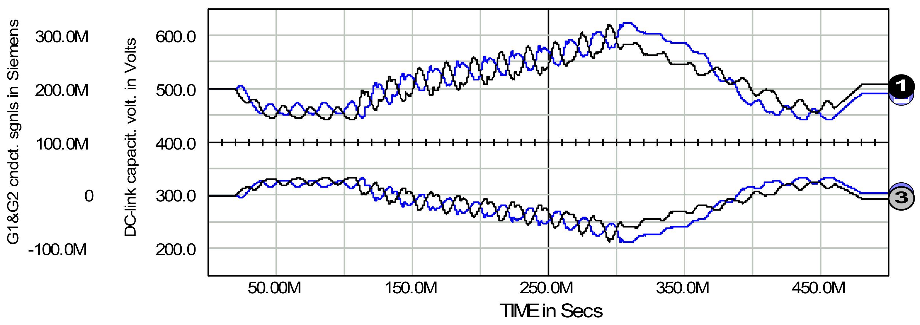
There is a specific effect of the inertial mode that should be mentioned. If this mode is active the active filter operates with grater mean-to-mean (or static) changes of DC-link capacitor voltage. This phenomenon is shown in Figure 16. In the extreme case, i.e., when the Tst parameter is increased excessively, the active filter may worsen, or even lose, its ability to shape of the source current, see DC-link capacitor voltage decreasing about the end of simulation.

7. Passive and Generative Load on the AC and DC Side of the System

The passive and/or generative load may be connected to the AC side as well as to the DC side of the active filter. Load phase currents and then the DC side current are shown in Figure 17.
The AC side part is of the same structure as that analyzed in Section 6.3, i.e., it consists of the passive part, of the generative part, and two current harmonics are also present. The passive part is activated at time t1 = 20 ms. The generative part is activated at time t2 = 100 ms and then deactivated at t3 = 400 ms. Both current harmonics start at 100 ms and are active till the end of simulation.
The DC side current is “distorted” from the classical DC circuit frame of reference. It is changeable in sign and contains an oscillating component. Generally, when the DC side current is positive it is then of generative type and supplies the DC-link capacitor with energy, and conversely if it is negative. Using other words, the active filter can also act as an energy bridge, connecting AC and DC loads and generators. Noticeable, DC side current influences the DC-link capacitor voltage and the conductance signal and, therefore, impacts AC side source currents.
The transmit, store and inertial modes of active filter operation have been introduced in Section 6. Benefits of using some combination of these modes are considered in Figure 18, Figure 19 and Figure 20 below.
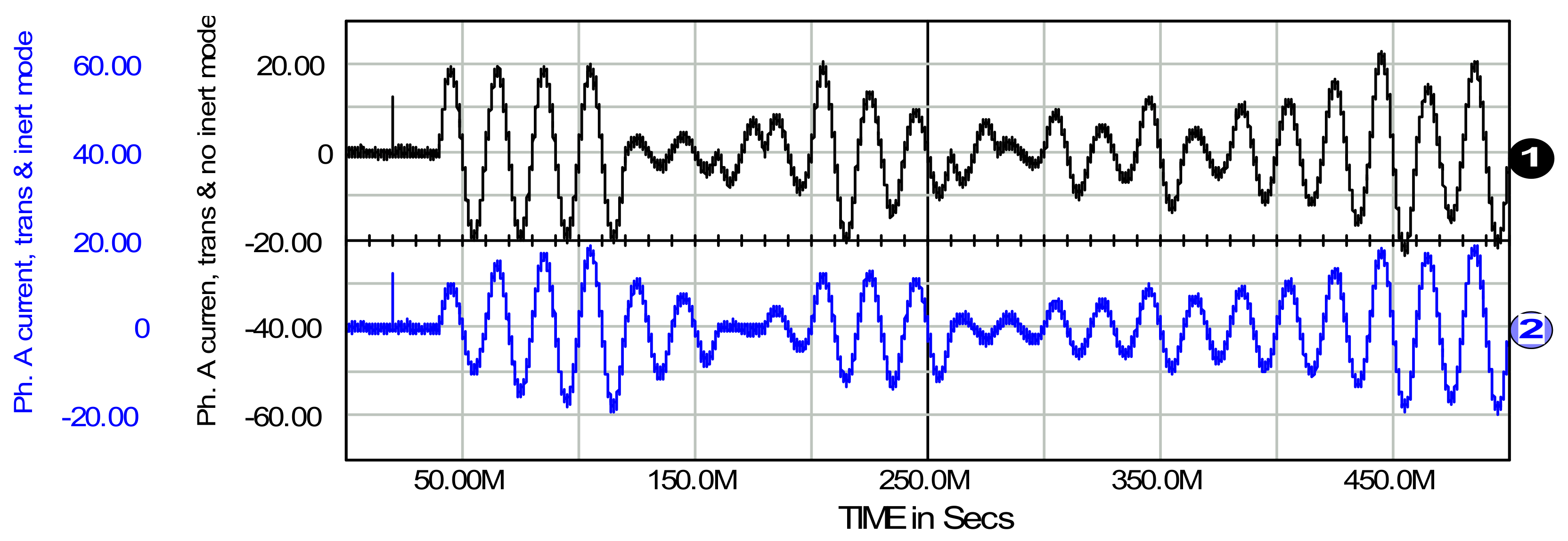
Figure 18: Since the compensated current are symmetrical, therefore—for simplicity—it is sufficient to show current of one phase of the source only, here current of the phase A. The active filter operates in the store mode without inertia, waveform 1, and then in combination of the store mode and inertia—the Tst parameter has been doubled with respect to its nominal magnitude, i.e., Tst = 2T now, waveform 2. As the result some stabilization of source current has been achieved: the rms of this current is decreased from 9.3 A to 8.0 A.
Figure 19: DC-link capacitor voltage waveforms for store mode and then for the store mode with inertia are presented. They correspond to the waveforms shown in Figure 18. The DC-link capacitor operates with lowered voltage if the inertial mode is used.
However, this lowered voltage is still sufficient for proper compensation for non-active component of source current, see waveform 2 in Figure 18.
Figure 20: Two modes of operation are compared in Figure 20. The active filter operates in the transmit mode without inertia, waveform 1, and then in combination of the transmit mode and the inertia (the Tst parameter has been doubled), waveform 2. The comparison of both waveforms shows that some stabilization of source current has been achieved. As the result the rms of the source current is decreased from 9.5 A, waveform 1, to 8.1 A, waveform 2.
As the general conclusion of this section it can be concluded that a combination of the transmit and store modes with the inertial mode of active filter operation can give positive effects, in particular in the decrease of rms parameters of source phase currents. Additionally, the power processing module of the active filter can also act as an energy bridge, which connects AC side and DC side loads and generators, and which operates at unity power factor at the AC side of the system.

8. Three-Phase Four Wire Active Filter

It is confirmed in this section that all the properties of the active filter control method with the use of the conductance signal, discussed so far for the three-phase three-wire system, are also valid for the three-phase four-wire system.
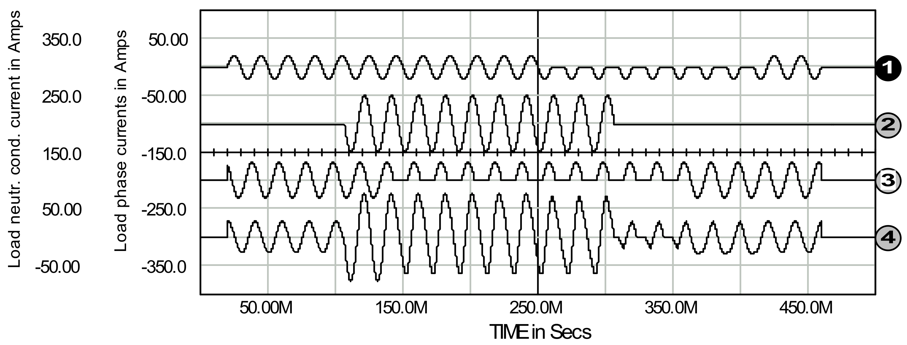
Time variable, nonlinear, unbalanced, passive, and generative load on the AC side of the system is considered. Load phase and neutral conductor currents of a three-phase four-wire load are shown in Figure 21. Phase currents of phase A and C (iLA and iLC in Figure 4), are in phase with respected phase voltages (they are of resistive type, partially of half-wave shape), but load phase current of phase B (iLB in Figure 4) is of generative type (it is reversed with respect to phase B voltage).
For time period 20 ms–460 ms, which is the whole cycle of load activity, the rms of load phase currents for phases A, B, and C are 13.5 A, 23.8 A, and 19.3 A, respectively. Buchholz equivalence for these currents is 33.4 A. Notice, Buchholz equivalence of all load currents (i.e., also including the neutral conductor current: iL0 in Figure 4, which rms is 36.1 A and mean is 2.9 A) is significantly higher and equals 49.3 A.
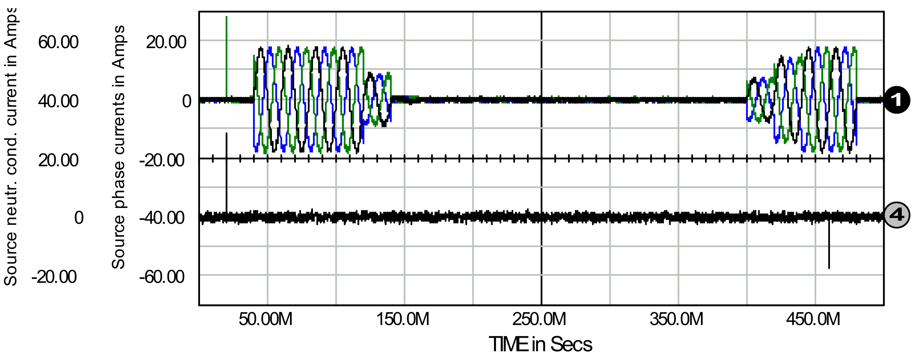
Source phase and neutral conductor currents for this load are shown in Figure 22. The active filter is configured to act in the store and no-inertial mode of operation. As the result of compensation source phase currents are sinusoidal and balanced, therefore there is no current in the source neutral conductor.
For period 40 ms–480 ms, i.e., for the whole cycle of the source work, Buchholz equivalence of source phase currents (iSA, iSB, and iSC in Figure 4) is 12.1 A—with respect to 33.3 A of load equivalent current. There is the same value of Buchholz norm if take into account also the source neutral conductor current—but this time it has been reduced from 49.3 A of all-conductors load current equivalence.
Both DC-link capacitor voltages, see voltages vC1 and vC2 in Figure 4, are shown in Figure 23. The conductance signals related to both voltage waveform are also presented in this figure. Some characteristic phenomena for the conductance signal control method can be seen in these voltage waveforms: static changes related to load power measuring, oscillating components related to compensation of non-active current components, oscillating components connected with balancing both DC-link capacitor voltages, supplying the load with the use of energy stored in the DC-link capacitor, and—at the end—returning of the voltages of both capacitors to the initial value after all loads are turned off.
There is an another possibility to configure the active filter to act in the transmit mode with limited power of upstream energy transmission to the AC side supply source. This mode of operation may be useful if there is too much of energy generated in the group of loads/generators being under active filter compensation and—in the same time—there is an energy demand on the AC side of the system outside of this group. This possibility is presented in Figure 24. The load is the same as in previous analysis in this section. For simplicity the active filter operates without inertia. The upstream power transmission limit is set—in terms of conductance signal—on the magnitude of 20 ms (negative in sign). This limiting effect can be seen in the time period 280 ms–300 ms, when the sampled, or the “in use” conductance signal, differs from the related-in-time magnitudes of the instantaneous one. The resulting amplitude of reversed source current is limited.
Notice, if the energy consuming in the load begins to exceed both the energy generated in the active part of the load and the excessive energy (i.e., the portion of energy that exceeds the initial magnitude) stored in the DC-link capacitor, then the conductance signal goes positive and the load is feeding from the supply source again.

9. Conclusions

The paper presents the functional properties of the active power filter controlled by the load equivalent conductance signal.
The main idea of the discussed controlled method is an attempt to achieve the goal of compensation using the simplest possible means. In order to achieve this, complicated methods of acquiring and sophisticated processing of a large number of input signals are proposed to be abandoned.
It was decided to use an indirect control method combined with a closed-loop structure of the current control circuit. Due to this choice, it is sufficient to measure practically one input quantity, i.e., to measure the voltage (energy) in the active filter DC-link capacitor, and to measure the output quantities, which are the source phase currents.
A detailed implementation of the considered active filter control method has not been discussed. It seems that the expressions (19)–(23), formulated in a universal mathematical language, constitute a fully readable instruction, according to which the idea of a conductive signal can be implemented in various ways. These implementations can be either analog or digital.
As a result of the conducted research, it was confirmed that the even relatively simple idea and its simple implementation allow for a significant improvement in the source current waveforms.
The considered method is universal from several points of view. It can be used in those active filters with a DC-link circuit of sufficiently high power and peak voltage (for VSI converters) or current (for CSI converters). Therefore, it can be successfully used in direct and alternating current circuits, as well as single and polyphase. Additionally, at the same time the active filter can regulate the energy flow between all sub-circuits of the system, constituting the local energy distribution center.

Funding

This research received no external funding.

Institutional Review Board Statement

Not Applicable.

Informed Consent Statement

Not Applicable.

Data Availability Statement

Not Applicable.

Conflicts of Interest

Author declares no conflict of interest.

References

  1. Green, T.C.; Marks, J.H. Control techniques for active power filters. IEEE Proc. Power Appl. 2005, 152, 369–381. [Google Scholar] [CrossRef] [Green Version]
  2. Asiminoaei, L.; Blaabjerg, F.; Hansen, S. Detection is key. Harmonic detection methods for active power filter applications. IEEE Ind. Appl. Mag. 2007, 13, 22–33. [Google Scholar] [CrossRef]
  3. Bhattacharya, A.; Chakraborty, C.; Bhattacharya, S. Shunt compensation. Reviewing traditional methods of reference current generation. IEEE Ind. Electron. Mag. 2009, 3, 38–49. [Google Scholar] [CrossRef]
  4. Khadkikar, V. Enhancing electric power quality using UPQC: A comprehensive overview. IEEE Trans. Power Electron. 2012, 27, 2284–2297. [Google Scholar] [CrossRef]
  5. Hoon, Y.; Radzi, M.A.M.; Hassan, M.K.; Mailah, N.F. Control algorithms for shunt active power filter for harmonics mitigation: A review. Energies 2017, 10, 2038. [Google Scholar] [CrossRef] [Green Version]
  6. Briz, F.; Garcia, P.; Degner, M.W.; Diaz-Reigosa, D.; Guerrero, M. Dynamic behavior of current controllers for selective harmonic compensation in three-phase active power filters. IEEE Trans. Ind. Appl. 2013, 49, 1411–1420. [Google Scholar] [CrossRef] [Green Version]
  7. Zhou, H.; Li, N.R.; Cheng, Z.; Ni, R.; Zhang, Y. Selective harmonic compensation (SHC) PWM for grid interfacing high-power converters. IEEE Trans. Power Electron. 2014, 29, 1118–1127. [Google Scholar] [CrossRef]
  8. Singh, B.; Verma, V. Selective compensation of power-quality problems through active power filter by current decomposition. IEEE Trans. Power Del. 2008, 23, 792–799. [Google Scholar] [CrossRef]
  9. Orts-Grau, S.; Gimeno-Sales, F.J.; Segui-Chilet, S.; Abellen-Garcia, A.; Alcaniz-Fillol, M.; Masot-Periz, R. Selective compensation in four-wire electric systems based on a new equivalent conductance approach. IEEE Trans. Ind. Electron. 2009, 56, 2862–2874. [Google Scholar] [CrossRef]
  10. Alfonso-Gil, J.C.; Perez, E.; Arino, C.; Beltran, H. Optimization algorithm for selective compensation in shant active power filter. IEEE Trans. Ind. Electron. 2015, 62, 3351–3361. [Google Scholar]
  11. Bhowmik, S.; van Zyl, A.; Spee, R.; Enslin, J. Sensorless current control for active rectifiers. IEEE Trans. Ind. Appl. 1997, 33, 765–773. [Google Scholar] [CrossRef]
  12. Nedeljkovic, D.; Nemec, M.; Drobnic, K.; Ambrozic, V. Active power filter with a reduced number of current sensors. Electrotech. Rev. 2009, 76, 275–280. [Google Scholar]
  13. Angulo, M.; Ruiz-Caballero, D.A.; Lago, J.; Heldwein, M.L.; Mussa, S.A. Active power filter control strategy with implicit closed-loop current control and resonant controller. IEEE Ind. Electron. 2013, 60, 2721–2730. [Google Scholar] [CrossRef]
  14. Ketzer, M.B.; Jacobina, C.B. Sensorless control technique for PWM rectifiers with voltage disturbance rejection and adaptive power factor. IEEE Trans. Ind. Electron. 2015, 62, 1140–1151. [Google Scholar] [CrossRef]
  15. Ketzer, M.B.; Jacobina, C.B.; Lima, A.M.N. Shaping control strategies for active power filters. IET Power Electron. 2018, 11, 175–181. [Google Scholar] [CrossRef]
  16. Sharma, S.; Verma, V.; Behera, R. Real-time implementation of shunt active power filter with reduced sensors. IEEE Trans. Ind. Appl. 2020, 56, 1850–1861. [Google Scholar] [CrossRef]
  17. Fukuda, S.; Kanayama, T.; Muraoka, K. A current control method for active filters without detecting current harmonics. In Proceedings of the Fifth International Conference on Power Electronics and Drive Systems, 2003, PEDS 2003, Singapore, 17–20 November 2003; Volume 1, pp. 519–524. [Google Scholar]
  18. Ozdemir, E.; Ucar, M.; Kesler, M.; Kale, M. A simplified control algorithm for shunt active power filter without load and filter current measurement. In Proceedings of the IECON 2006—32nd Annual Conference on IEEE Industrial Electronics, Paris, France, 7–10 November 2006; pp. 2599–2604. [Google Scholar]
  19. Nedeljkovic, D.; Nemec, M.; Drobnic, K.; Ambrozic, V. Direct current control of active power filter without filter current measurement. In Proceedings of the 2008 International Symposium on Power Electronics, Electrical Drives, Automation and Motion, Ischia, Italy, 11–13 June 2008; pp. 72–76. [Google Scholar]
  20. Ketzer, M.B.; Jacobina, C.B. Multivariable load current sensorless controller for universal active power filter. IET Power Electron. 2014, 7, 1777–1786. [Google Scholar] [CrossRef]
  21. Noguchi, T.; Tomiki, H.; Kondo, S.; Takahashi, I. Direct power control of PWM converter without power-source voltage sensors. IEEE Trans. Ind. Appl. 1998, 34, 473–479. [Google Scholar] [CrossRef]
  22. Ketzer, M.B.; Jacobina, C.B. Virtual flux sensorless control for shunt active power filters with quasi-resonant compensators. IEEE Trans. Power Electron. 2016, 31, 4818–4830. [Google Scholar] [CrossRef]
  23. Wojciechowski, D. Grid voltages sensorless control system of the PWM rectifier with active filtering function. In Proceedings of the IEEE Compatibility in Power Electronics, Gdynia, Poland, 6 January 2005; pp. 238–246. [Google Scholar]
  24. Choi, W.-H.; Lam, C.-S.; Wong, M.-C.; Han, Y.-D. Analysis of dc-link voltage controls in three-phase four-wire hybrid active power filters. IEEE Trans. Power Electron. 2013, 28, 2180–2191. [Google Scholar] [CrossRef]
  25. Lam, C.-S.; Choi, W.-H.; Wong, M.-C.; Han, Y.-D. Adaptive dc-link voltage controlled hybrid active power filters for reactive power compensation. IEEE Trans. Power Electron. 2012, 27, 1758–1772. [Google Scholar] [CrossRef]
  26. Tarkiainen, A.; Pollanen, R.; Niemela, M.; Pyrhonen, J. DC-link voltage effects on properties of a shunt active filter. In Proceedings of the 35th Annual IEEE Power Electronics Specialists Conference, Aachen, Germany, 20–25 June 2004. [Google Scholar]
  27. Longhui, W.; Fang, Z.; Pengbo, Z.; Hongyu, L.; Zhaoan, W. Study on the influence of supply-voltage fluctuation on shunt active power filter. IEEE Trans. Power Del. 2007, 22, 1743–1749. [Google Scholar] [CrossRef]
  28. Bitoleanu, A.; Popescu, M.; Dobriceanu, M.; Nastasoiu, F. DC-bus voltage optimum control of three-phase shunt active filtering system. In Proceedings of the 12th International Conference on Optimization of Electrical and Electronic Equipment, OPTIM 2010, Brasov, Romania, 20–22 May 2010. [Google Scholar]
  29. Sharma, S.; Verma, V. Modified control strategy for shunt active power filter with MRAS-based DC voltage estimation and load current sensor reduction. IEEE Trans. Ind. Appl. 2021, 57, 1652–1663. [Google Scholar] [CrossRef]
  30. Moreno, V.; Pigazo, A. Modified FBD method in active power filters to minimize the line current harmonics. IEEE Trans. Power Del. 2006, 22, 735–736. [Google Scholar] [CrossRef]
  31. Strzelecki, R.; Benysek, G.; Jarnut, M. Power quality conditioners with minimum number of current sensor requirement. Przegląd Elektrotechniczny (Electrotech. Rev.) 2008, 84, 295–298. [Google Scholar]
  32. Szromba, A.; Mysinski, W. Voltage-source-based conductance-signal controlled shunt active power filter. In Proceedings of the 2017 European Conference on Power Electronics and Applications, Warsaw, Poland, 11–14 September 2017. [Google Scholar]
  33. Szromba, A. The Unified Power Quality Conditioner Control Method Based on the Equivalent Conductance Signals of the Compensated Load. Energies 2020, 13, 6298. [Google Scholar] [CrossRef]
  34. Fallah, M.; Modarresi, J.; Kojabadi, H.M.; Chang, L.; Guerrero, J.M. A modified indirect extraction method for a single-phase shunt active power filter with smaller DC-link capacitor size. Sustain. Energy Technol. Assess. 2021, 45, 101039. [Google Scholar]
  35. Dixon, J.W.; Ooi, B.T. Indirect current control of a unity power factor sinusoidal current boost type three-phase rectifier. IEEE Trans. Ind. Electr. 1988, 35, 508–515. [Google Scholar] [CrossRef]
  36. Nunez-Zuninga, T.; Pomilio, J. Shunt active power filter synthesizing resistive loads. IEEE Trans. Power Electron. 2002, 17, 273–278. [Google Scholar] [CrossRef]
  37. Hamadi, A.; Al-Haddad, K.; Lagace, P.; Chandra, A. Indirect current control techniques of three phase APF using fuzzy logic and proportional integral controller: Comparative analysis. In Proceedings of the 11th International Conference on Harmonics and Quality of Power, Lake Placid, NY, USA, 12–15 September 2004. [Google Scholar]
  38. Fei, J.; Li, T.; Zhang, S. Indirect current control of active power filter using novel sliding mode controller. In Proceedings of the IEEE 13th Workshop on Control and Modelling for Power Electronics, Kyoto, Japan, 10–13 June 2012. [Google Scholar]
  39. Ribeiro, R.; Azevedo, C.; Sousa, R. A robust adaptive control strategy of active power filters for power-factor correction, harmonic compensation, and balancing of nonlinear loads. IEEE Trans. Power Electron. 2012, 27, 718–730. [Google Scholar] [CrossRef]
  40. Trinh, Q.; Lee, H. An advanced current control strategy for three-phase shunt active power filter. IEEE Trans. Ind. Electron. 2012, 60, 5400–5410. [Google Scholar] [CrossRef]
  41. Ribeiro, R.; Rocha, T.; Sousa, R.; dos Santos, E.; Lima, A. A robust DC-link voltage control strategy to enhance the performance of shunt active power filters without harmonic detection schemes. IEEE Trans. Ind. Electron. 2014, 62, 803–813. [Google Scholar] [CrossRef]
  42. Wu, T.-F.; Chang, C.-H.; Lin, L.-C.; Yu, G.-R.; Chang, Y.-R. DC-bus voltage control with a three-phase bidirectional inverter for DC distribution systems. IEEE Trans. Power Electron. 2013, 28, 1890–1899. [Google Scholar] [CrossRef]
  43. Szromba, A. Shunt power electronic buffer as active filter and energy flow controller. Arch. Electr. Eng. 2013, 62, 55–75. [Google Scholar] [CrossRef] [Green Version]
  44. Grabowski, D.; Maciążek, M.; Pasko, M. Sizing of active power filters using some optimization strategies. COMPEL 2013, 32, 1326–1336. [Google Scholar] [CrossRef] [Green Version]
  45. Depenbrock, M.; Staudt, V. The FBD-method as tool for compensating non-active currents. In Proceedings of the 8th International Conference on Harmonics and Quality of Power, Athens, Greece, 14–16 October 1998; pp. 320–324. [Google Scholar]
  46. Fryze, S. Wirk-, Blind-, und Scheinleistung in Elektrischen Stromkreisen mit nichtsinusformigem Verlauf von Strom und Spannung. Elektrotechnische Z. 1932, 25, 33. [Google Scholar]
  47. Singh, B.; Chandra, A.; Al-Haddad, K. Performance comparision of two current control techniques applied to an active filter. In Proceedings of the 8th International Conference on Harmonics and Quality of Power, Athens, Greece, 14–16 October 1998; pp. 133–138. [Google Scholar]
  48. Herrera, R.; Salmeron, P.; Kim, H. Instantaneous reactive power theory applied to active power filter compensation: Different approaches, assessment, and experiment result. IEEE Trans. Ind. Electron. 2008, 55, 185–196. [Google Scholar] [CrossRef]
  49. Mishra, M.; Joshi, A.; Ghosh, A. Control schemes for equalization of capacitor voltages in neutral clamped shunt compensator. IEEE Trans. Power Del. 2003, 18, 538–544. [Google Scholar] [CrossRef] [Green Version]
  50. Montero, M.; Cadaval, E.; Gonzalves, F. Comparision of control strategies for shunt active power filters in three-phase four-wire systems. IEEE Trans. Power Electron. 2007, 22, 229–236. [Google Scholar] [CrossRef]
  51. Sozański, K. Improved shunt active power filters. Przegląd Elektrotechniczny (Electrotech. Rev.) 2008, 11, 290–294. [Google Scholar]
  52. Sozański, K.; Strzelecki, R.; Kempski, A. Digital control circuit for active power filter with modified instantaneous reactive power control algorithm. In Proceedings of the Power Electronics Specialists Conference PESC, Cairns, Australia, 23–27 June 2002; pp. 1031–1036. [Google Scholar]
  53. Urrea-Quintero, J.-H.; Munoz-Galeano, N.; Lopez-Lezama, J.M. Robust control of shunt active power filter: A dynamical model-based approach with verified controllability. Energies 2020, 13, 6253. [Google Scholar] [CrossRef]
  54. Intusoft. Better Design Through Simulation. Available online: www.intusoft.com (accessed on 16 September 2021).
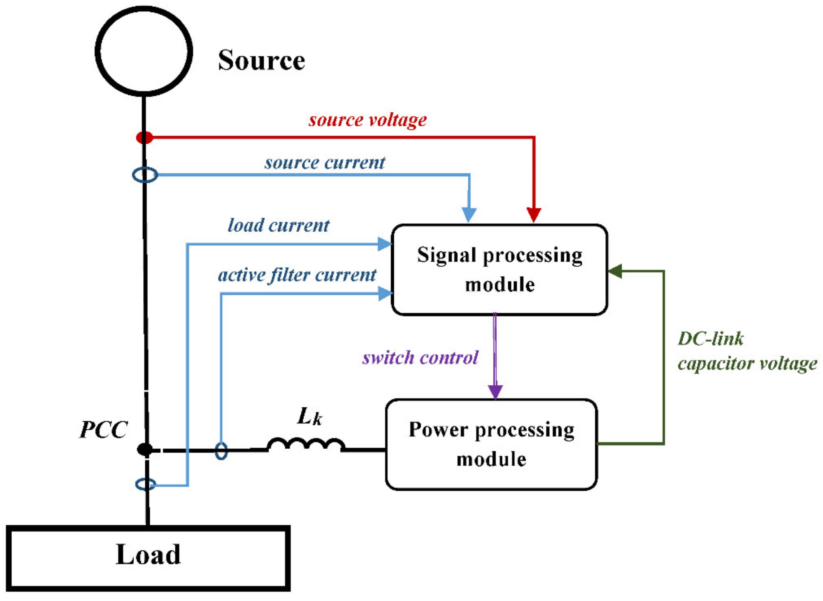
Figure 1. Source-line-load circuitry with active power filter block diagram. Active filter modules and its signal tracks are shown in single-phase system conventionality. PCC is the point of common coupling.
Energies 14 06031 g001
Figure 2. Basic scheme of three-phase three-wire circuit with active power filter.
Energies 14 06031 g002
Figure 3. FBD theory approach. Conductance gD signal, waveform 1, and Depenbrock phase power currents, waveforms 2, 3, and 4 in phase A, B and C, respectively.
Energies 14 06031 g003
Figure 4. Three-phase four-wire source-line-load circuitry with active filter.
Energies 14 06031 g004
Figure 5. Load phase currents of phase A, B and C: waveforms 1, 2 and 3, respectively. The load passive part is switched on at t1 = 20 ms, and the generative part is activated at t2 = 100 ms.
Energies 14 06031 g005
Figure 6. Source phase currents of phase A, B and C as waveforms 1, 2, and 3, respectively; and then the conductance signal (22): waveform 4.
Energies 14 06031 g006
Figure 7. DC-link capacitor voltage: waveform 1, and conductance signal (22): waveform 4. The passive part of the load is switched on at t1 = 20 ms, and the generative part is activated at t2 = 100 ms.
Energies 14 06031 g007
Figure 8. Load phase currents of phase A, B, and C as waveforms 1, 2, and 3, respectively.
Energies 14 06031 g008
Figure 9. Source phase currents of phase A, B, and C as waveforms 1, 2, and 3, respectively, against the background of phase A source voltage.
Energies 14 06031 g009
Figure 10. Total instantaneous load power: waveform 1 (in black); instantaneous source phase powers: waveforms 2, 3, and 4 (all in blue); three-phase source total power: waveform 5; DC-link capacitor voltage: waveform 6.
Energies 14 06031 g010
Figure 11. Source phase currents of phase A, B, and C as waveforms 1, 2, and 3, respectively, against the background of source voltage.
Energies 14 06031 g011
Figure 12. Total instantaneous load power: waveform 1 (in black); source phase powers: waveforms 2, 3, and 4 (all in blue); total source power: waveform 5; DC-link capacitor voltage: waveform 6.
Energies 14 06031 g012
Figure 13. Load phase currents of phase A, B, and C as waveforms 1, 2, and 3, respectively. The load passive part is switched on at t1 = 20 ms, and the generative part is activated at t2 = 60 ms and deactivated at t3 = 320 ms.
Energies 14 06031 g013
Figure 14. Source phase currents of phase A, B, and C as waveforms 1, 2, and 3, respectively, and the conductance signal, waveform 4.
Energies 14 06031 g014
Figure 15. Source phase currents of phase A, B, and C as waveforms 1, 2, and 3, respectively, and the conductance signal, waveform 4.
Energies 14 06031 g015
Figure 16. DC-link capacitor voltage at nominal magnitude of Tst: waveform 1, and then at triple increased Tst magnitude: waveform 2.
Energies 14 06031 g016
Figure 17. AC side load phase currents: waveforms 1–3, Y scale is 50 A/div for these currents; and DC side load current: waveform 4, Y scale is 20 A/div.
Energies 14 06031 g017
Figure 18. AC side source phase A current for store mode without inertia: waveforms 1, and for Scheme 2. Y scale for currents is 10A/div.
Energies 14 06031 g018
Figure 19. DC-link capacitor voltages. Store mode without inertia: waveforms 1, and store mode in combination with inertia: waveforms 2.
Energies 14 06031 g019
Figure 20. AC side source phase A current for transmit mode without inertia: waveforms 1, and for transmit mode in combination with inertia: waveform 2. Y scale for currents is 10A/div.
Energies 14 06031 g020
Figure 21. Load phase A, B, and C currents: waveforms 1–3, respectively, and load neutral conductor current: waveform 4.
Energies 14 06031 g021
Figure 22. Source phase currents: waveforms 1–3, and load neutral conductor current: waveform 4.
Energies 14 06031 g022
Figure 23. DC-link capacitor voltages: waveforms 1 and 2, and load conductance signals based on both DC-link capacitor voltages: waveforms 3 and 4.
Energies 14 06031 g023
Figure 24. Analog conductance signal: waveform 1 (in black), sampled conductance signal: waveform 2 (in blue) and source phase A current: waveform 3 (in green).
Energies 14 06031 g024
Publisher’s Note: MDPI stays neutral with regard to jurisdictional claims in published maps and institutional affiliations.