Abstract
In this work, an idea of a wideband, precision, power electronics programmable voltage source (PVS) is presented. One of the basic elements of the converter, the control section, contains a continuous-time sigma-delta modulator (SDM) with a pair of interconnected complementary comparators, which represents a new approach. In this case, the SDM uses comparators with a dynamic hysteresis loop (DHC) that includes an AC circuit rather than an R-R network. Dynamic hysteresis is a very effective way of eliminating parasitic oscillation during the signal transition at the input of the comparator; it also affects the frequency characteristics and, especially, the phase properties of the comparator, and this phenomenon is exploited in the proposed converter. The main disadvantage of all pulse-modulated converters is the presence of a ripple component in the output voltage (current), which reduces the quality of the output signal and may cause high-frequency disturbances. A basic feature of PVS is a lower RMS value for the pulse modulation component in the output voltage of the converter, compared to the typical value. Another important feature of the proposed converter is the ability of precise mapping of the output voltage to the reference (input) signal. The structure of the control circuit is relatively simple—no complex, digital components are used. Due to the high frequency of the SDM output bit-stream, the simulation model of the power stage of PVS is based on the power modules with gallium-nitride field effect transistors (GaN FETs). The work discusses the rules of PVS operations and the results from PVS simulation model studies as well as highlights the possible application fields for systems with a PVS.
1. Introduction
Nonlinearities in loads, limited frequency responses for power electronics converters, and the wide-band nature of both signal sampling and pulse modulation processes are some of the possible reasons for inaccurate mapping of a converter’s output voltage to a reference signal. To address this problem, advanced converter solutions are necessary, in terms of both hardware and control algorithms. One approach is to implement a sigma-delta modulator (SDM) in the converter structure [1,2,3]. Several variants of the SDM technique are widely used in precision A/D and D/A converters [1,4,5], audio class-D amplifiers [6,7,8], including the current-mode operation of its power stage [9], special-purpose measurement techniques [10], current measurement for motor control [11], and many other areas of industrial electronics [12]. This technique can also be used to control many types of power electronics devices, including matrix converters [13], commonly used converters for LED lighting [14], multilevel converters [15], and converters for power systems with renewable energy sources [16]. Most of these SDMs are discrete-time systems, i.e., systems applying a quantization of signals over time (e.g., [1,2]). The main disadvantage of all pulse-modulated converters is the presence of a ripple component in the output voltage (current), which reduces the quality of the output signal and may cause high-frequency disturbances. The solution to this problem is to use an LC output filter, however, a reduction in its cut-off frequency reduces the frequency response of the entire converter. However, minimising the magnitude of the ripple voltage is also possible through the use of an appropriate converter control strategy.
In this paper, the proposal of a self-exciting, continuous-time SDM with a pair of interconnected dynamic hysteresis comparators (DHCs) to control the output stage of a power electronics programmable voltage source (PVS) [17,18] is presented. The basic premise of the proposed power electronics system is to obtain a precise mapping of the output voltage to the reference (input) signal. Special attention is given to minimising the energy of the ripple voltage in the converter’s output signal, which is caused by a carrier component of pulse modulation. In addition, the structure of the control block is simple, mostly analogue (i.e., no typical digital components are used in the SDM), and can be easily implemented in power electronics devices, in which a high-quality output quantity (voltage, current) is necessary. Similarly to the case of SDMs with a static hysteresis comparator, the output signal of an SDM-DHC is also both pulse-width- and pulse-duration-modulated (PWM and PDM, respectively) [1,12,19,20]. Dynamic hysteresis is a very effective way of eliminating parasitic oscillation during the signal transition at the input of the comparator; it also affects the frequency characteristics and, especially, the phase properties of the comparator (and SDM), a phenomenon that is exploited in the proposed converter. In theory, due to the analogue nature of the SDM-DHC, its resolution tends toward infinity. In addition, unlike in SDMs based on a static hysteresis comparator, the minimal width of the output pulses is limited to a certain pre-set value in the case of the DHCN (where DHCN denotes the DHC in the signal non-inverting version while DHCI is related to the comparator in the signal-inverting version) [17,18]. This value depends on the time constant of the DHCN, meaning that this circuit is insensitive to high-frequency pulses (e.g., noise) at its input. Consequently, it is expected that this converter will be more resistant to electromagnetic disturbances, compared to a system based on a comparator with static hysteresis. As a result of most of these assumptions, the distortion in the PVS output voltage is much lower than in typical (i.e., PWM-based) converter solutions [17,19,20]. Due to the very high frequency (about 1 MHz) of the SDM output bit-stream, models of the new generation of intelligent power modules (IPM), based on GaN power FETs, are used in the power stage of the simulation model of the converter. The more detailed description of this device is given in Section 3.
The remainder of the paper is divided into four sections. Section 2 deals with the rules of operation and parameters of PVS based on the SDM-DHC. Section 3 is devoted to a description of the converter models used in the simulation tests. In Section 4, the results of simulation investigations and a discussion is presented. The final section is devoted to the conclusions.
2. Operation of a PVS
2.1. Topology and Basic Features of SDM-DHC
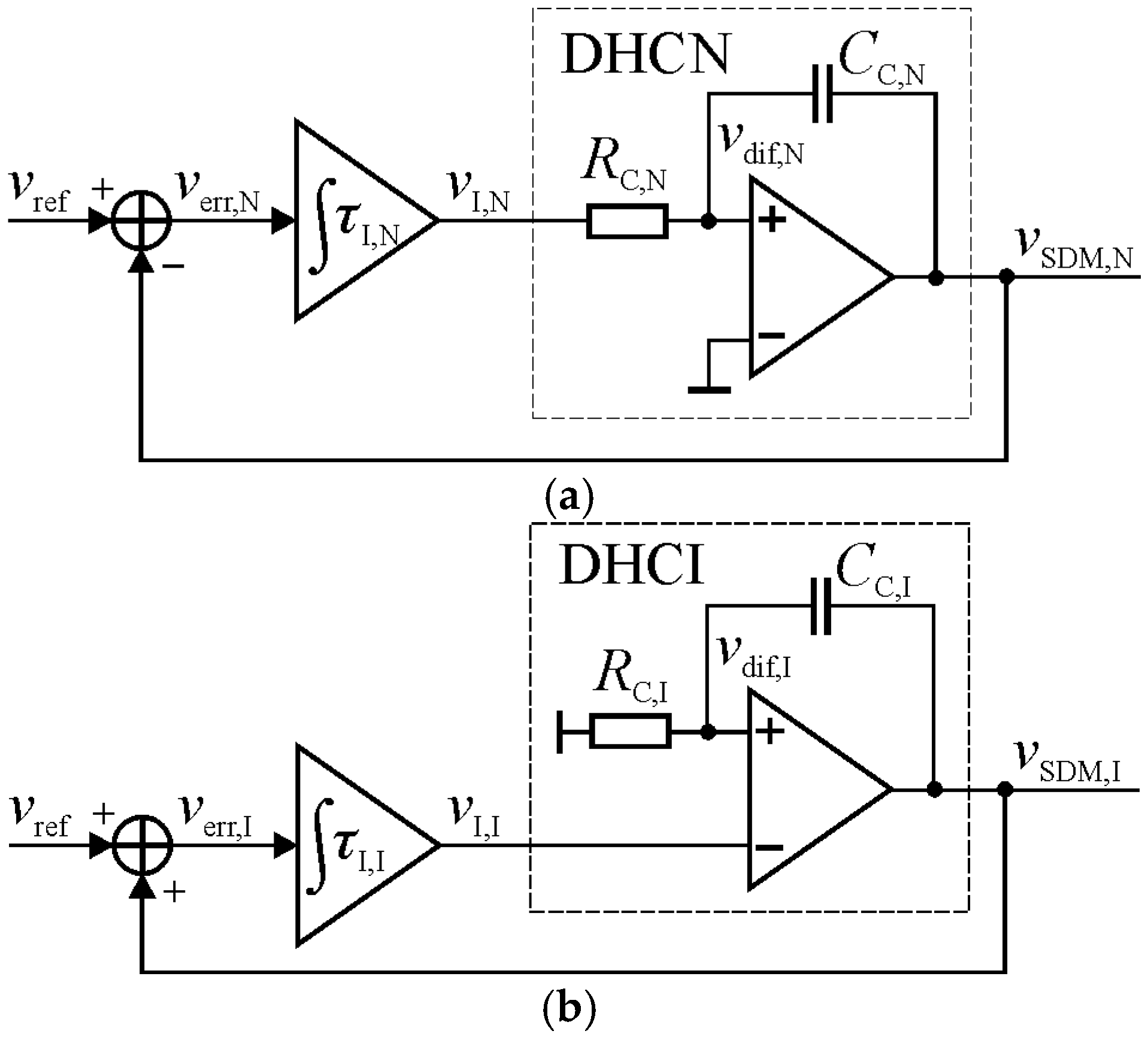
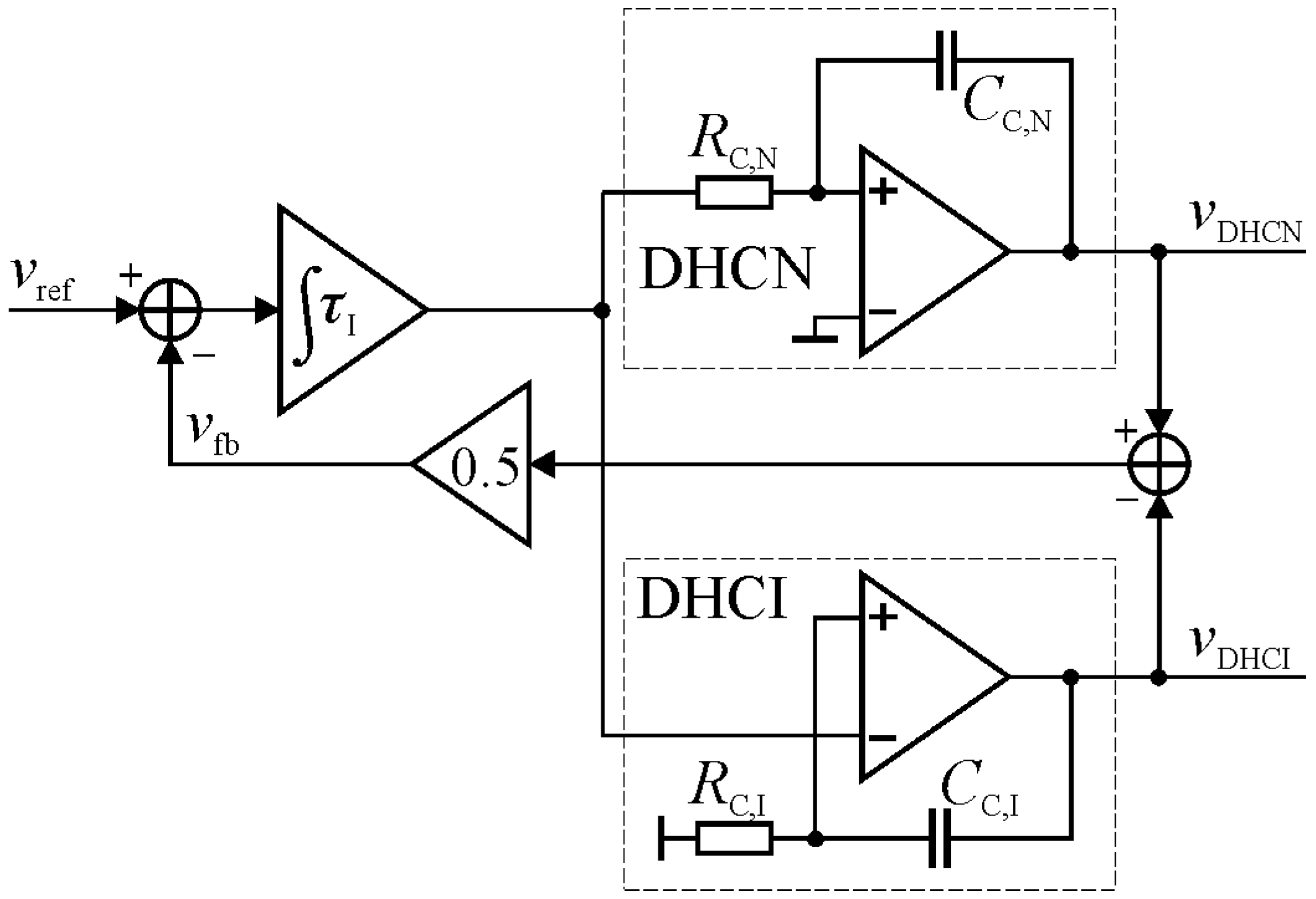
The details of the operation of an SDM based on a DHC have been presented in previous works [17,18], and only a brief description of this system structure and its basic features are given here for the reader’s convenience. Figure 1 shows both versions of the SDMs.

Figure 1.
Block diagrams of an SDM with DHC in the (a) signal non-inverting and (b) signal inverting versions.
Although each SDM contains similar blocks (a signal adder, an integrator, and a DHC), these are connected in different ways. A converter power stage is typically included at the output of the DHC, however, this block is not shown in the figure due to the power stage not being necessary for operation of the SDM in its basic form.
The SDM is very difficult to analyse in the time domain, due to the apparent randomness of the single-bit data output, meaning that the system is both nonlinear and time variant [1,21,22]. The simplified models of SDMs, in the frequency domain, are typically used. These models are also used for system stability analysis. Hence, a strict analytical description of the SDM operation is difficult; most of the formulas and relationships included in this work were obtained based on heuristic methods [23,24] and were confirmed using simulation studies and laboratory models tests.
The basic properties of an SDM in the signal non-inverting and signal inverting versions, respectively, are as follows:
- The periods of the SDM output signal are:where , , and is a pulse modulation index, which is defined as:where is the magnitude of the reference signal, is the value of the converter power supply voltage, and is the converter gain for DC.
- The relationships between the integrator time constant and the comparator time constant, which protects the output of the integrator against entering a saturation (signal clipping) state, are:
- The minimal width of the DHC input signal, being passed through itself (assuming that the shape of the DHC input signal is the same as the shape of output signal, i.e., the rectangular and magnitudes of both signals are equal to each other), is:
- The cut-off frequencies of the integrator are:
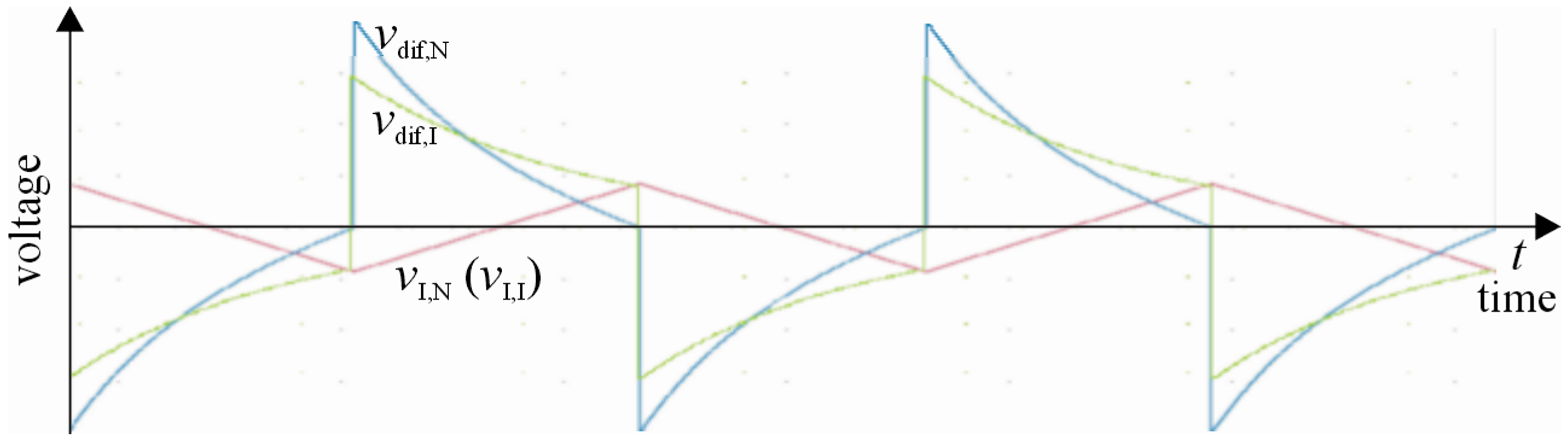
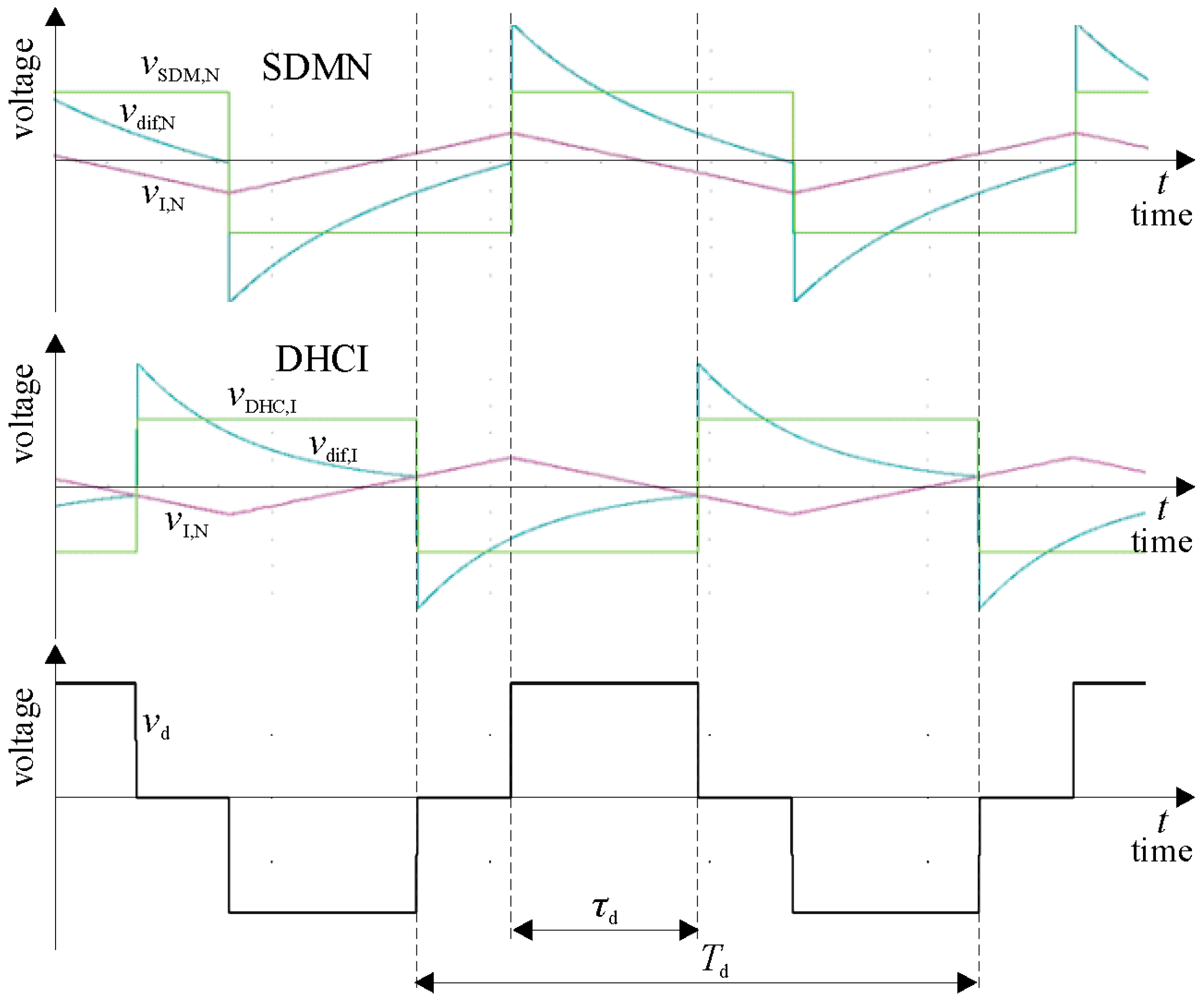
To maximise the converter frequency response, the time constant of the integrator (, ) should be as small as possible while respecting the conditions in (4) and (5). The relationships between the integrator and comparator time constants, given in (4) and (5), result from the different characteristics of the signals in the DHCN and DHCI circuits [2]. This is illustrated in Figure 2, where the waveforms for the SDM-DHCN and SDM-DHCI are shown, based on the assumptions that = , = 2.0 (this relationship represents the boundary dependence of the time constants of the comparators, as a result of (4) and (5)), and = 0. Since the DHCs differ from each other in terms of the operation of the AC circuits (- and -), the two types of SDM have some complementary properties, and their dynamic parameters are defined by suitable time constants (, ). It is also worth noting that (6) and (7) mean that the DHCN is a low-pass device, while the DHCI is close to an all-pass device in nature, which affects the properties of the PVS.
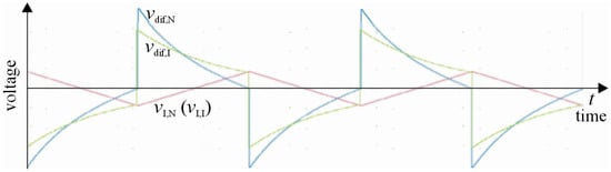
Figure 2.
Characteristic waveforms for the SDM-DHCN and SDM-DHCI circuits, assuming: = , = 2.0, and = 0.
The SDM generates a PWM similar signal with a carrier period, the value of which depends on the time constants of both the integrator and the DHC. The value of this period varies with the magnitude of the input signal to the SDM (i.e., modulation index), as shown in Figure 3. The values given for the relationship between the time constants of the integrator and DHC are exemplary ones, but they indirectly result from (4) and (5).
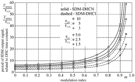
Figure 3.
Ratio of the SDM carrier period and DHC time-constant vs. the modulation index.
The frequency of the SDM switching pattern has a spread-spectrum nature; however, as the amplitude of the input signal decreases, this spectrum focuses more closely on the value given by (1) (or (2)). Spread-spectrum techniques are often used to distribute emissions over a wider frequency range [25,26]. If , the signal accompanied exclusively by the pulse modulation process (i.e., the carrier component) appears at the output of the SDMs. Whereas, if > 0.7, the reduction in the carrier frequency becomes clearly visible.
In Figure 4, the ratio of the SDM-DHCN and SDM-DHCI carrier periods is plotted against the modulation index, assuming that the initial value (i.e., for = 0) of these periods is = . The studies of DHC simulation models, respecting (1) and (2), indicate that this equality can only be achieved if the following relationship is met:
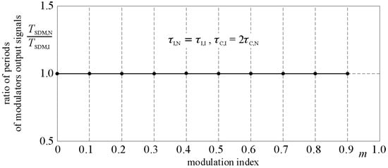
Figure 4.
Ratio of the SDMN and SDMI carrier periods vs. the modulation index.
The curve in Figure 4 shows that the changes in the values of the carrier periods vs. the modulation index are proportionally the same for both types of SDM.
2.2. Operation of the DHCI as a Phase Shifter
As a result of the operation of the DHCs, the pulse modulation carrier components, at the outputs of the DHCN and DHCI, are shifted in time relative to each other. This conclusion has an important impact on further considerations, related to the use of the SDMs in the proposed PVS. To illustrate the effect of phase shifting of the DHC output signal, a dedicated test circuit was used, as shown in Figure 5.
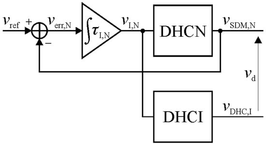
Figure 5.
Diagram of the circuit with DHCI, operating as a phase shifter of its output signal.
In the structure of the test circuit, the SDM is composed of the integrator and the DHCN. The DHCI also operates on the integrator’s output signal, but acts as a phase shifter of the voltage. The basic waveforms in this circuit are shown in Figure 6.

Figure 6.
Example waveforms for the SDM-DHCN (upper image) and DHCI (central image), and the differential signal at the outputs of the SDM-DHCN and DHCI (lower image), assuming = and .
Waveforms denoted as and are the internal signals of the DHCI and DHCN, respectively. These signals are indicated in Figure 1—the diagrams of the SDMs.
Assuming , the relative phase shift () in the SDM-DHCN and DHCI output signals is defined as follows:
where is the period of the SDM carrier component and is the shift in time of the DHCI output voltage, in relation to the SDM-DHCN output signal.
This relationship forms the basis of operation of the proposed converter with reduced voltage ripples in its output voltage.
The RMS value of the carrier component (), assuming , is given by the following equation:
where is the magnitude of this component.
Hence, as decreases, the root-mean-square value of the carrier component also decreases.
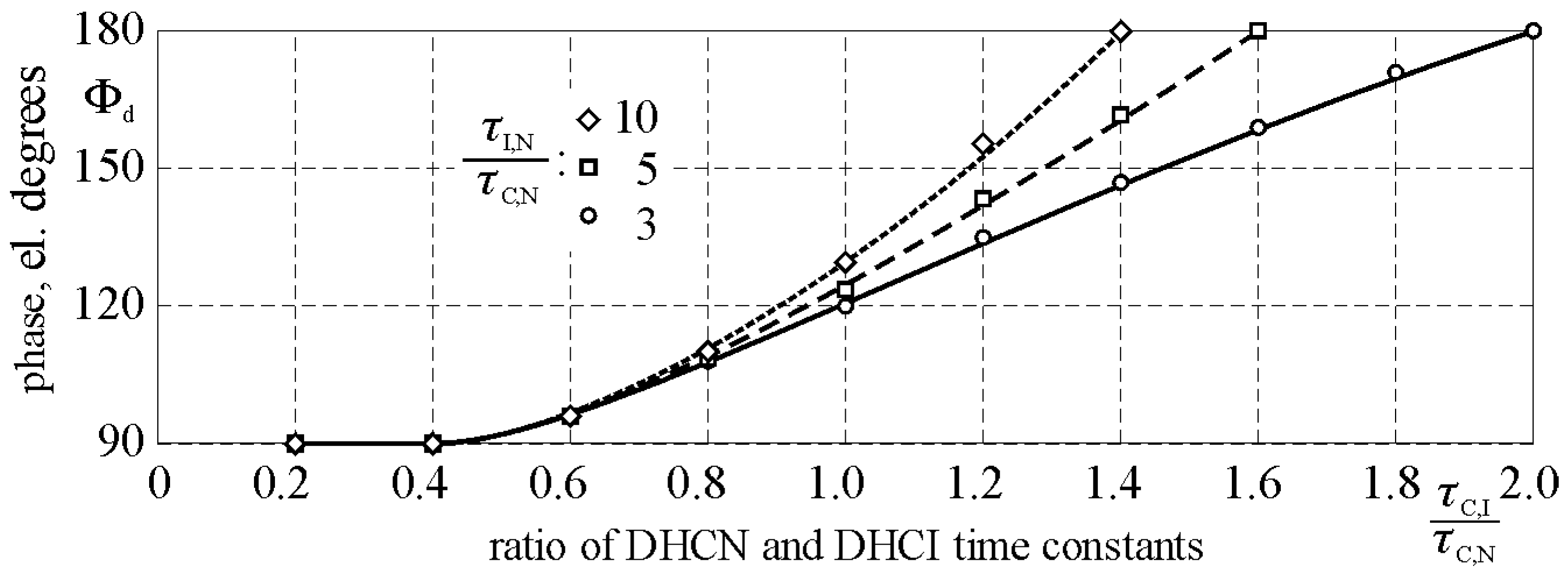
The value of the phase shift mainly depends on the ratio of to , and somewhat less on the ratio of to . In the circuit shown in Figure 5, it is possible to achieve a phase shift in the range of 90–180 el. degrees (Figure 7).
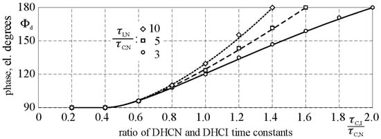
Figure 7.
Relative phase shift in the SDM-DHCN and DHCI output signals vs. the ratio of and , assuming .
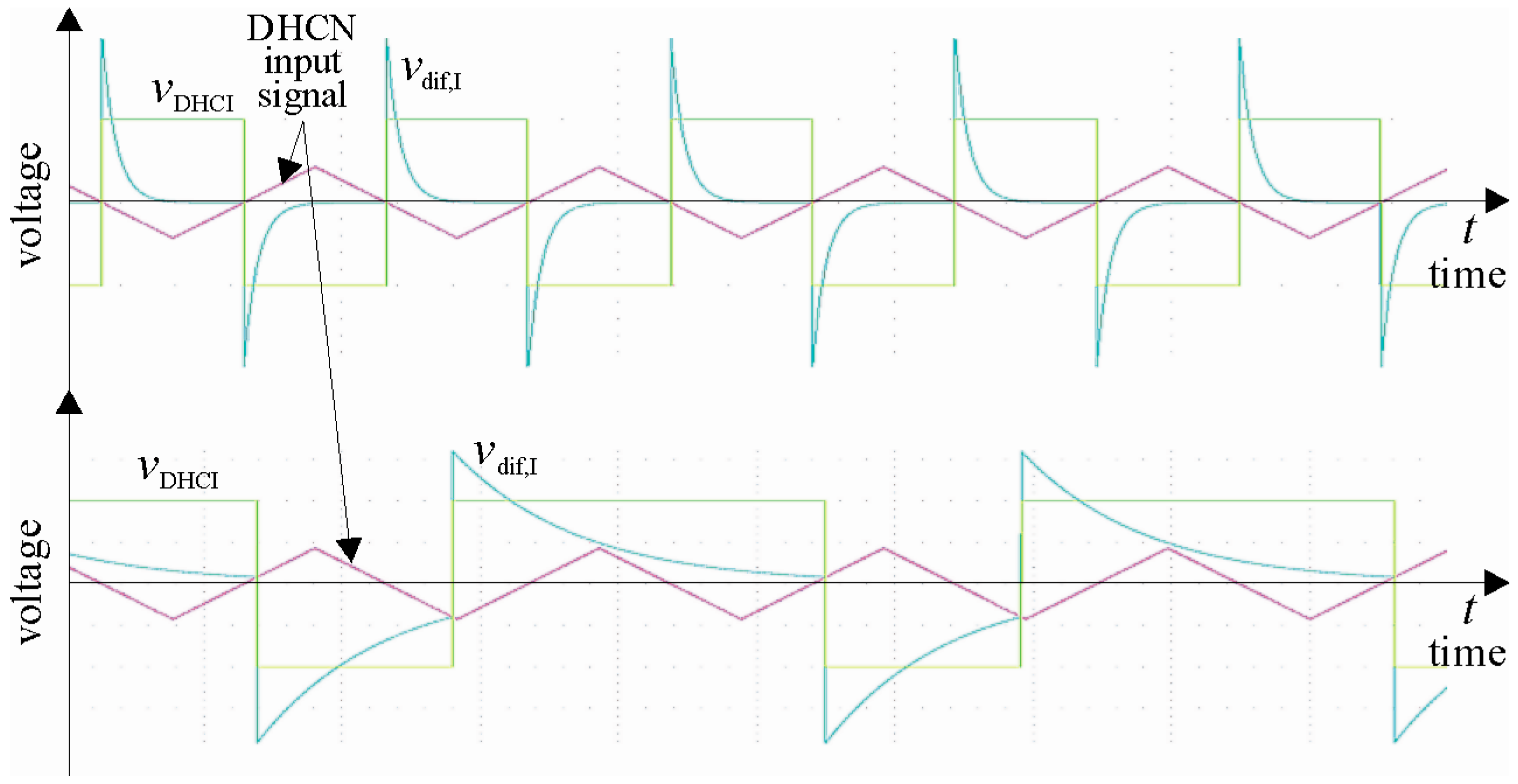
The ratio of and is limited to a certain maximal value, and exceeding this causes the DHCI to “lose” the output pulses, as shown in Figure 8 (lower image).
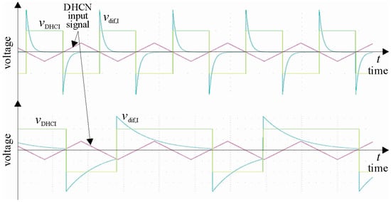
Figure 8.
Example waveforms for the DHCN, assuming: = 0, = 3.0; = 0.5 (upper image), and = 2.2 (lower image).
For example, when = 3, the following relationship must be met: . This feature of the DHCN results from the low-pass nature of the circuit, as described above. By minimising the value of , the energy of the pulse modulation carrier component is also minimised. For instance, if , the RMS value of the carrier component is reduced by 30%, compared to the system with no phase shifting of the output signal.
The main disadvantage of this configuration of the SDM and DHCI is that the DHCI operates in an open feedback loop, meaning that the output signal of the DHCI may be affected by nonlinear distortions. Further modification to the PVS topology is therefore necessary, and this is described in the following section.
2.3. Control Block for PVS with Reduced Ripple Voltage
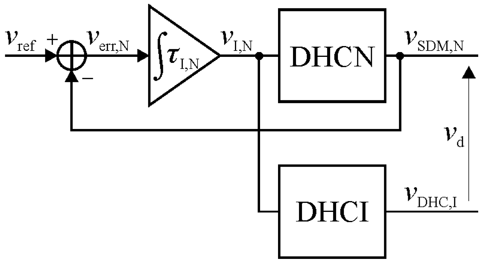
Comparative studies of several converter structures have been carried out with a focus on selecting a converter control block topology to minimise the RMS value of the pulse modulation component, compared to a typical converter [17,18,19,20]. At the same time, the high quality of the output voltage, in relation to the reference signal needs to be ensured. On the basis of these studies, the final topology for the converter control section was chosen, as shown in Figure 9. For this system, the range of the phase shift, achieved in the output signals of the comparators, was even greater than for the system described in the previous section.
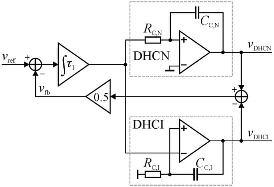
Figure 9.
PVS with reduced ripple voltage component—block diagram of the converter control section.
The most important feature of this circuit is that it uses both types of DHCs, which enforces a partially differential structure of the PVS. In this case, both comparators are connected to the output of the integrator and all circuits operate in voltage type, feedback loop. The feedback voltage () is defined as: = 0.5. The operation of the converter is controlled by the three time constants, , , and , and the values of the signal parameters in the PVS result from the interdependencies between these time constants.
Since a strict analytical description of the operation of the proposed PVS in the time domain is a very complex problem, heuristic methods were used to achieve this task. At this stage of the investigations, the models of the main internal components of the PVS (operational amplifiers) were simplified, i.e., did not include any parasitic elements. On the basis of these methods (respecting (1) and (2)), the following relationship between the time constants was derived:
This represents a particular case of the operation of this system, which is characterised by the lowest possible magnitude of the ripple component in the output signal (understood as the differences of and —Figure 9) and low distortion of this voltage in relation to the reference signal.
3. Simulation Studies of the PVS Model
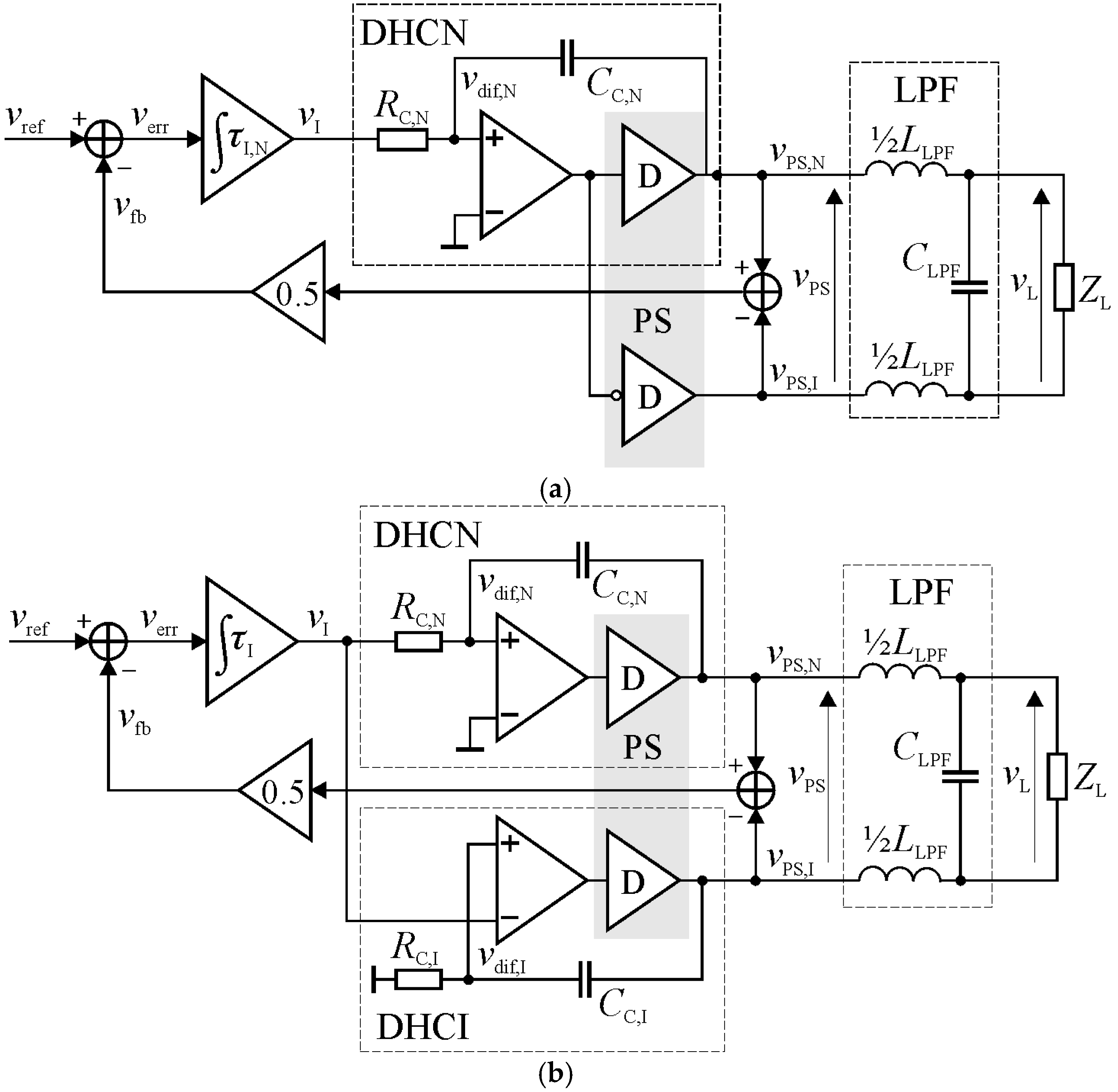
Comparative studies of the two converter topologies were carried out using the ORCAD/Spice environment, on both the standard (reference) converter (SPVS) and the proposed PVS with reduced ripple component of the output voltage (R2PVS). The main purpose of these tests was to confirm the achievement of the assumed R2PVS parameters, i.e., a reduction in the ripple component of the output voltage, a suitable frequency response, and low nonlinear distortion of the converter output voltage. Diagrams of both models are shown in Figure 10.
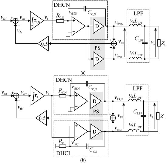
Figure 10.
Simplified block diagrams of (a) SPVS and (b) R2PVS, which form the basis for simulation models of the converters.
The SPVS uses a single DHC, and its output power stage (PS) consists of a complementary pair of drivers (D). These models therefore differ mainly in terms of the configuration of the control circuit, while the power stage and output filter (LPF) are the same (or very similar). However, a low-pass output filter is often based on a single inductor, or the role of this filter may be played by an RL type of load (such as a loudspeaker [27]).
In the full version of a simulation model, the output voltage of PS needs to be limited to a certain value. This value results directly from the voltage at the DC rails that supply the PS; it was assumed that the supply voltage was bipolar and equal to . Therefore, (assuming ) the following equations define values of the phase shift and the pulse modulation component of the output voltage of both models:
where is the shift in time of and , and is the period of the voltage .
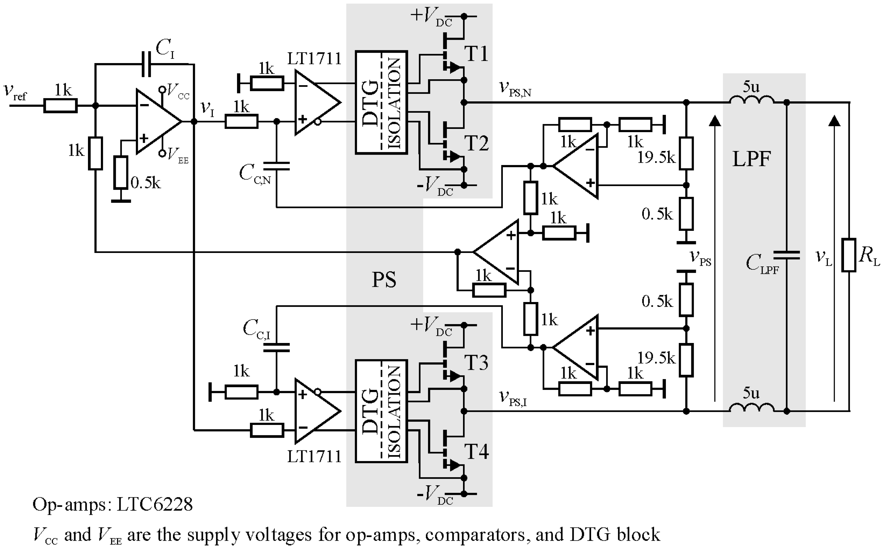
A more detailed diagram of the converter, which formed the basis for the final simulation models, is shown in Figure 11. Although this diagram represents the R2PVS, it is also possible to reconfigure its structure to represent the SPVS. As a consequence, for both models, the internal devices (blocks) were the same, in order to ensure a high level of reliability for the results of the comparative studies.

Figure 11.
Diagram of the PVS with real devices, as used as a basis for the detailed simulation models.
The list of the most important components which models were used in the simulation tests is as follows:
- LTC6228 (Analog Devices)—ultra-fast (730 MHz, 500 V/μs), rail-to-rail output, stable unity gain, operational amplifier, specified for a power supply range of 2.8–11.75 V [28];
- LT1711 (Analog Devices)—ultra-fast (4.5 ns), rail-to-rail inputs and rail-to-rail complementary output comparator; specified for a power supply of ±5 V [29];
- ADuM121N0 (Analog Devices) digital isolators (CMTI = 100 kV/μs typical) specified for a power supply of at 5 V [30] (used in the DTG block);
- LMG3411R070—intelligent power module (IPM), containing a GaN power FET with integrated driver [31], manufactured by Texas Instruments—used in the converter’s power block. The integrated gate driver enables a scalable slew rate for the IPM output voltage, which is typically in the range of 25–100 V/ns. This device also provides the over-current and over-temperature protection for the GaN FET chip.
However, only basic, static and dynamic, parameters of the listed devices were respected in the simulation model of the converter. They were: simplified frequency response, propagation time, and, in the case of op-amps and comparators, input offset voltage and input bias current. In the author’s opinion, taking into account the purpose of the simulation models research, such simplifications are acceptable. Nevertheless, the approaches to testing simulation models of converter systems are very diverse—depending on the purpose of the research. An example may be the work devoted to modeling the DC/DC converter, also using GaN devices [32].
4. Test Results and Discussion
In this section, the results of the simulation tests and a discussion of the results are presented. The values of parameters are related to application of the PVS as a medium power class-D audio amplifier:
- SPVS: = 600 ns ( = 600 pF), = 200 ns ( = 200 pF), and = 400 ns ( = 400 pF);
- R2PVS: = 300 ns ( = 300 pF), = 100 ns ( = 100 pF), and = 280 ns ( = 280 pF); Common parameters: = 95 V; = 220 nF (characteristic frequency of the LPF = 107 kHz); rated magnitude of the reference voltage = 5 V; = = 4 Ohm; rated output power: = 1000 W; supply voltages of the control circuit (, ): 5 V; and dead time (generated in the DTG block) for GaN transistors in the PS: = 35 ns.
The values of the other passive components used in the model are given in Figure 11. Taking into account the values of these parameters and assuming that the initial properties of both systems are the same (i.e., for ), the value of the carrier frequency is equal to approx. 1 MHz.
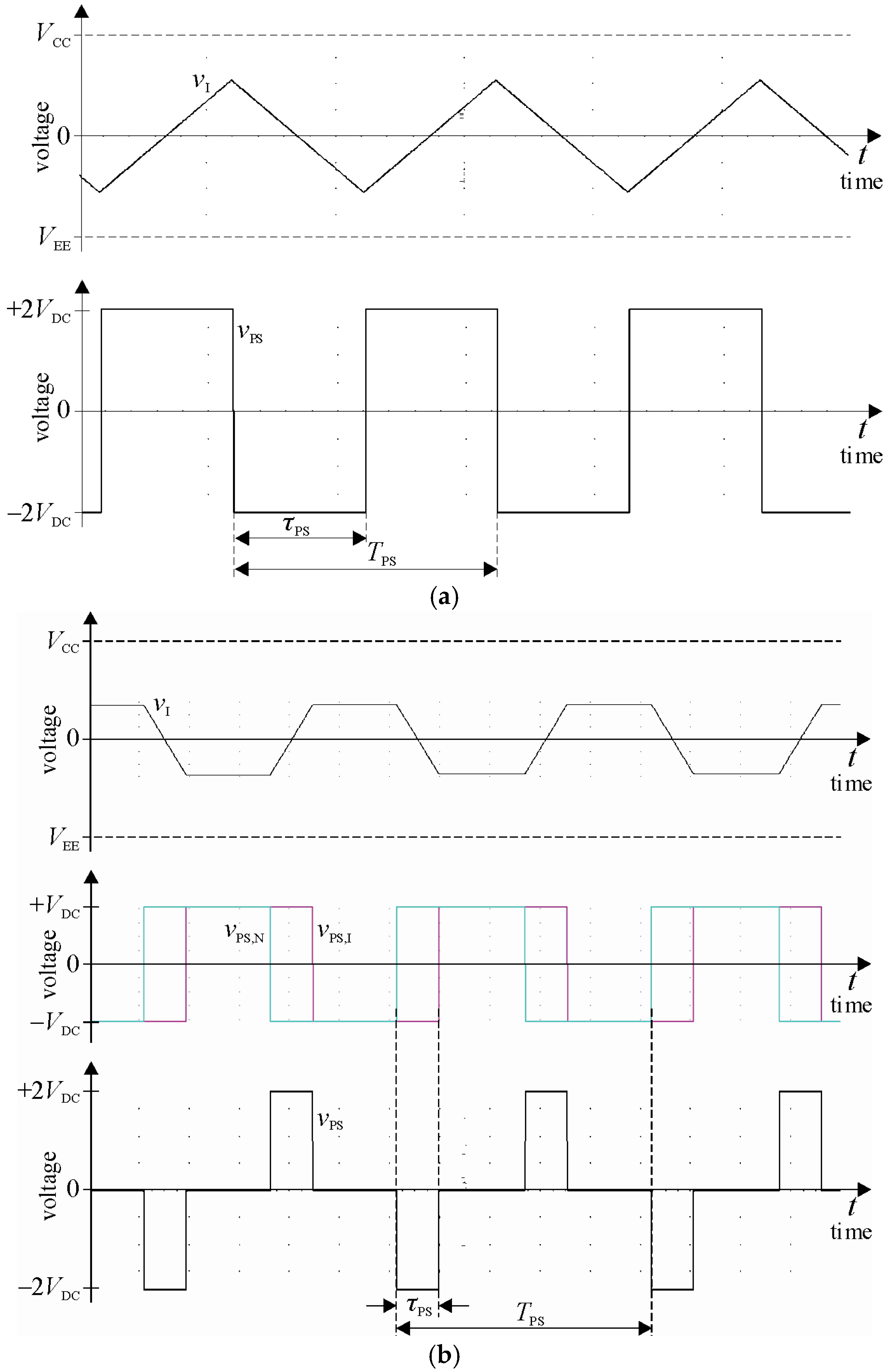
Figure 12 shows the waveform at the integrator output and the carrier component at the power stage output, for both versions of the PVS.
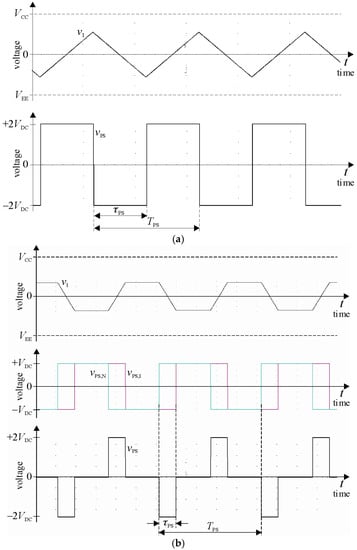
Figure 12.
Waveforms from the simulation model of the PVS, assuming , for (a) SPVS and (b) R2PVS.
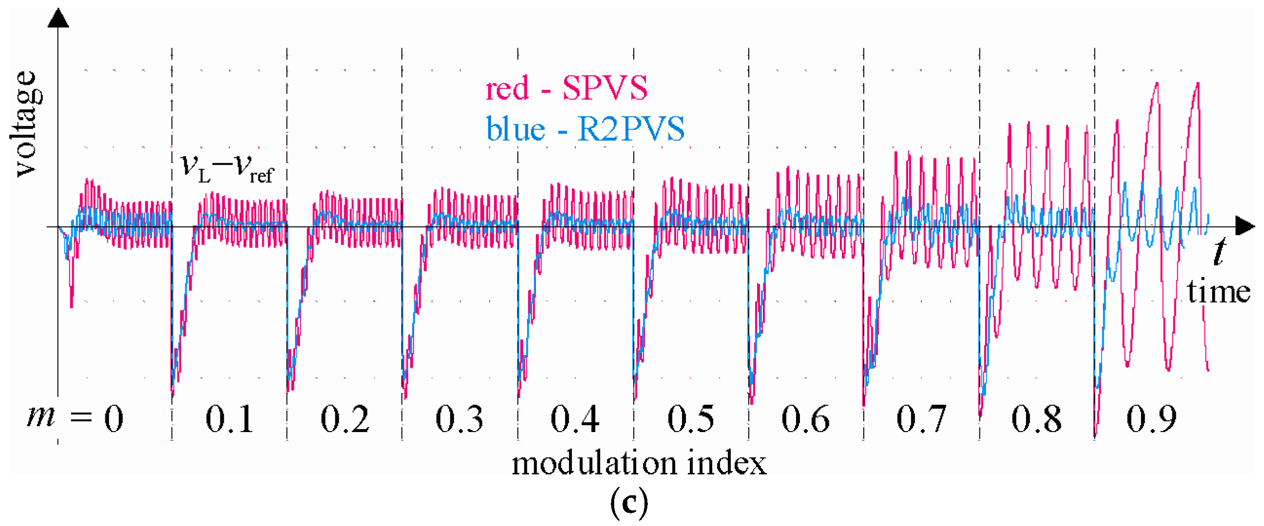
The most important factor for the operation of the converter is the relative phase shift of the and signals. For the SPVS, = 180 el. degrees, while for R2PVS, = 62 el. degrees. Thus, the RMS value of the carrier component for the R2PVS is equal to 59% of the value for the SPVS.
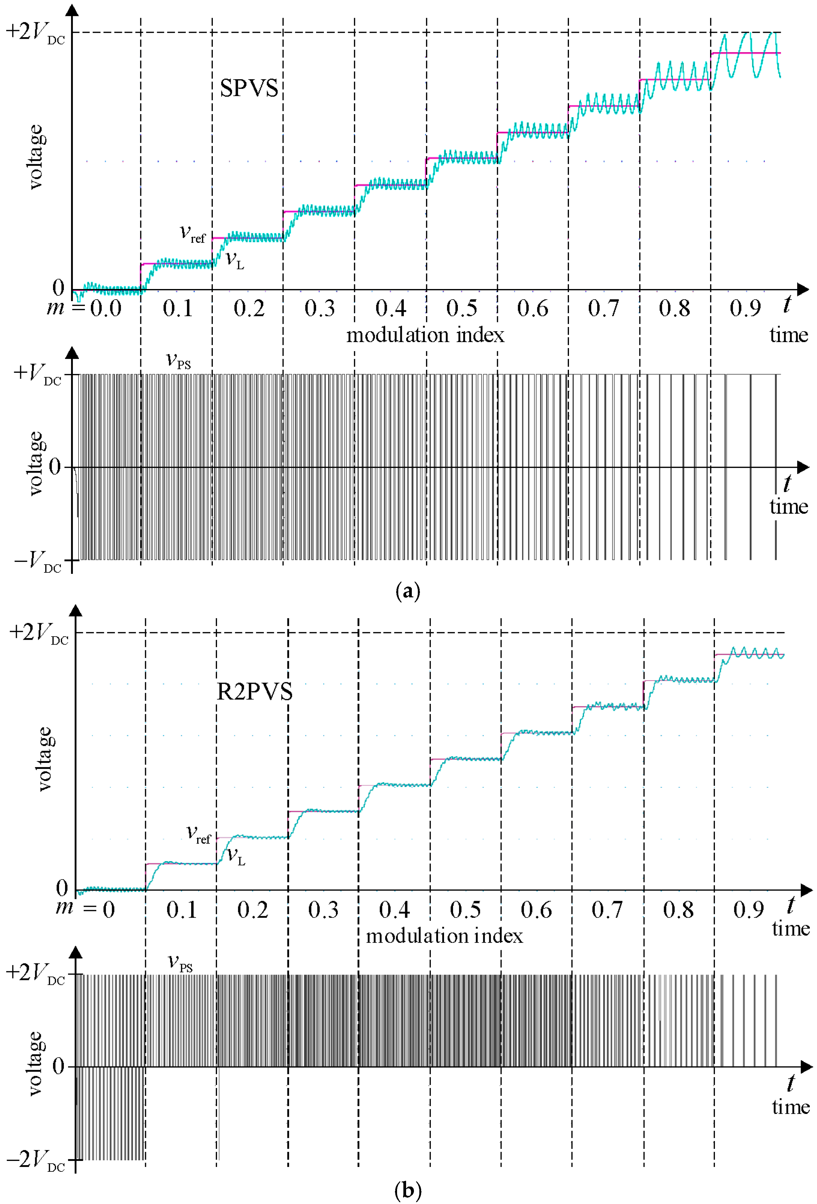
Figure 13 is one of the most important in this paper. It shows the relationship between the instantaneous value of the carrier component at the output of the LPF, against the modulation index, for both types of converters, as this index is varied over the full range of operation of the converter. For better visualization of these waveforms the magnitude of the reference signal is scaled by a factor of , according to (3). Thanks to the highly set value of the cut-off frequency of the output filter, the ripples of the output voltage are exposed, which facilitates an analysis of their RMS value.
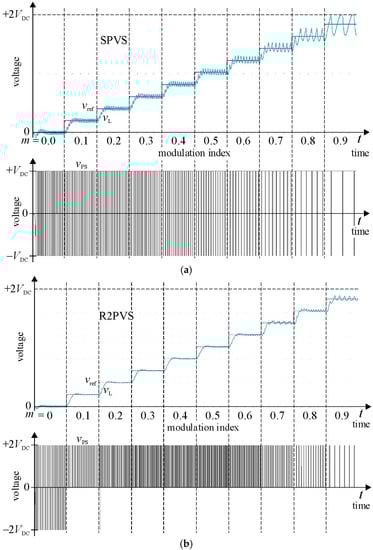
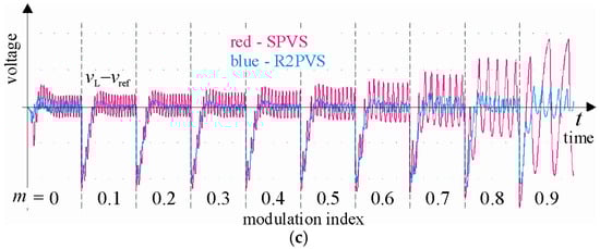
Figure 13.
Waveforms from the simulation models of (a) SPVS and (b) R2PVS, and (c) superimposed waveforms of the carrier component for both models.
It can clearly be seen that in the case of the R2PVS, the voltage at the power stage output over a wide range of (except of = 0) is very similar to the output voltage of an H-bridge (the inverter containing of a pair of branches, i.e., equipped with four of power switches), controlled in a PWM-unipolar mode [19,20]. This kind of modulation gives a much more desirable spectrum for the output voltage, compared to PWM-bipolar modulation [19,20], as in the case of SPVS. Due to this, the calculated value of the RMS of the carrier component is much lower (by a factor of 1.7–5.0, depending on ) for the R2PVS output voltage than for the SPVS.
Figure 14 shows the waveform for the large-signal step response of the R2PVS. For the SPVS, the waveform of the output voltage was almost consistent with the voltage shown in this figure.
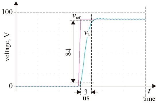
Figure 14.
Large-signal step response for R2PVS.
Based on these results, it was possible to calculate the value of the large-signal bandwidth () parameter for the models, which is defined as [1]:
where is the magnitude of the output voltage and is the change in this voltage over a time interval .
Using the model parameters mentioned above, and under nominal conditions of operation for the converters, ≅ 52 kHz. The value of can be increased, but at the expense of increasing the magnitude of the pulse modulation component of the output voltage of the converter(s).
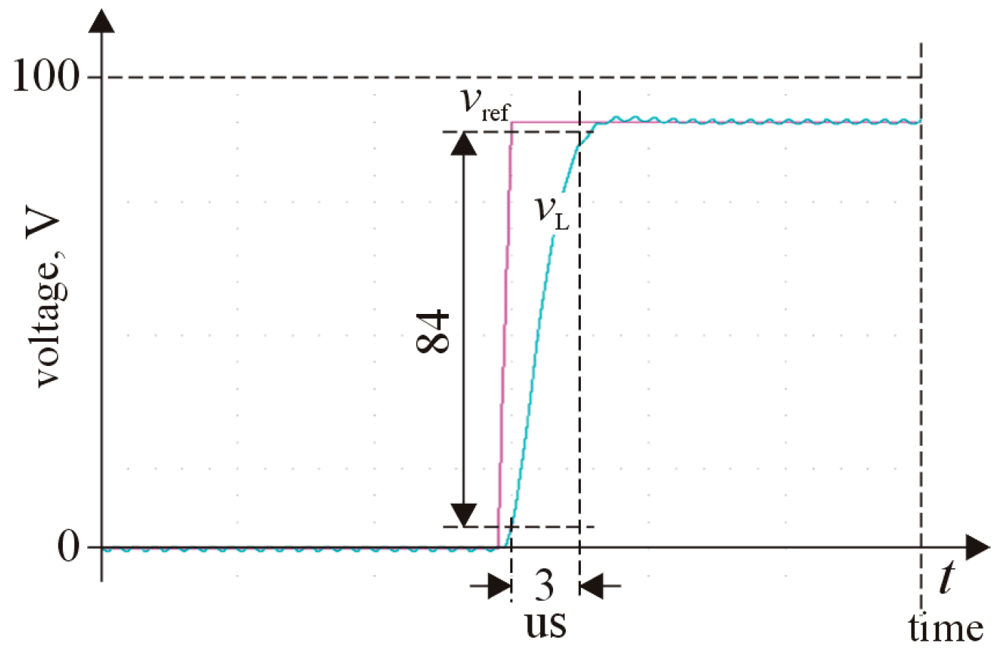
Figure 15 shows the characteristic waveforms in the simulation model of the R2PVS, where the reference signal is a sine-wave, with frequency () that is close to the upper limit of the converter frequency response, = 50 kHz. The amplitude of this signal was set to 90% of its nominal value.
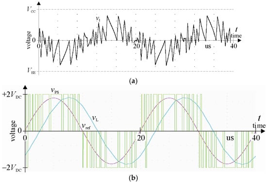
Figure 15.
Characteristic waveforms in the R2PVS while the input signal is sine-wave: (a) signal at integrator output, (b) reference signal (red), voltage at the output of power stage (green), and converter’s output voltage (blue), assuming = 50 kHz and = 4.5 V.
All waveforms indicate proper operation of the proposed PVS, and show that the output voltage from the integrator is not clipped. The value of this voltage stays in the range with a safe margin, equal to approximately 20% of the power supply voltage.
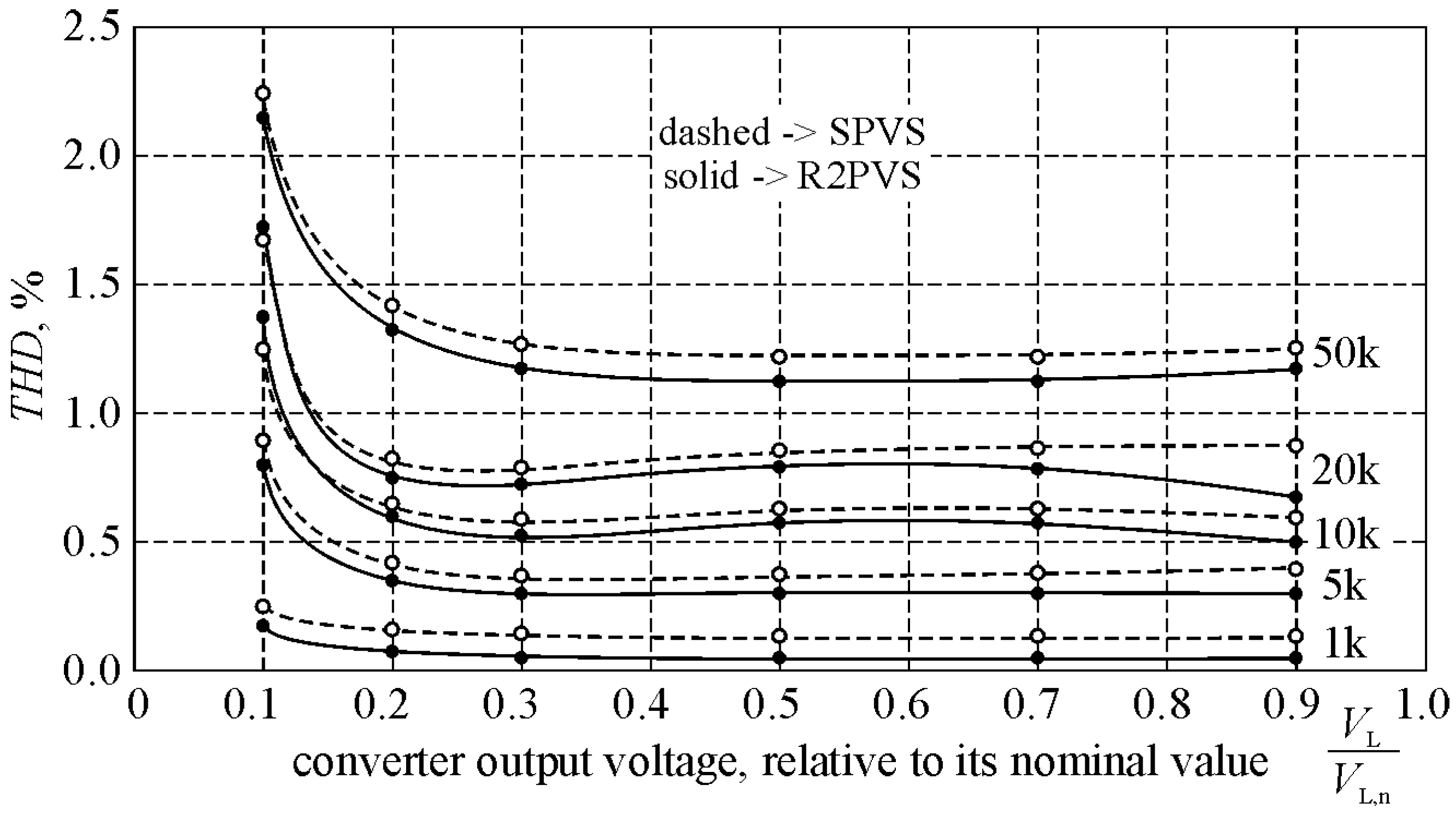
Figure 16 shows the curves for the (Total Harmonic Distortion [19,20]) factor of the output voltage, for both converters. In this case, the amplitude of the sine-wave reference signal varies between 10% and 90% of its nominal value. To determine the , the first 10 harmonics of the output voltage were respected. These tests were conducted for the following values of the reference signal frequency: 1, 5, 10, 20, and 50 kHz.
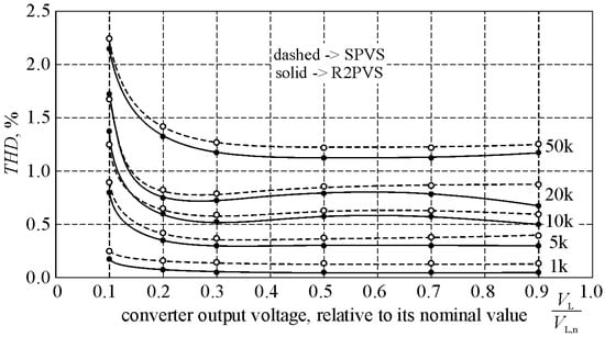
Figure 16.
Factor of the converters output voltages vs. amplitude of this signal, related to its nominal value, while reference signal frequency varies.
The calculated values of the factor are very similar for both converters. This factor falls within the range 0.05–2.3%, and decreases when the reference signal basic frequency is decreased. This is a natural phenomenon which arises due to the increase in the gain of the converter’s control block as the frequency decreases. When the amplitude of the reference signal is above 20% of the nominal value, the falls toward the minimal value.
In general, the findings of the PVS simulation models indicate a good mapping of the PVS output voltage to the reference signal, for both types of converters, under the condition that the significant harmonics of the output voltage are in the range of .
5. Conclusions
The results from the simulation model of the proposed PVS aligned well with the theoretical assumptions made for this converter. The proposed converter is characterised by a significantly lower value (by a factor of up to five) for the RMS of the ripples in the output voltage (current) caused by a pulse modulation, compared to a standard converter. Reduction in the pulse modulation component lets extend the life-time of the power line and the loads connected to it. Also, it is expected that the proposed device will be able meet the EMC requirements more easily, compared to a standard converter’s solution. Moreover, in addition to the technical context, this issue should be considered in terms of a purely economic and even social (e.g., health) impact.
The simulation model studies also showed that the PVS based on a sigma-delta modulator (in the control block), in which the comparator(s) have a dynamic hysteresis loop and the power stage with GaN FETs, is characterised by a very wide pass band. It should also be noted that, in both types of converters analysed here, the values of this parameter were very similar. As a consequence, the output voltage of a PVS of this type can be precisely mapped to a reference signal, which is also the result of the much higher resolution of the continuous-time SDM, compared to a typical PWM block - taking into account the high value of the pulse modulation carrier frequency. For example, in the case of the well-recognized ADSP-21369, the digital signal processor (SHARC® family, Analog Devices, Inc., Boston, MA, USA) [33], assuming the core clock frequency of 400 MHz (i.e., the maximum value for this device), the effective resolution of the PWM block falls to 7.5 bits. This value is completely insufficient in high-precision applications.
The structure of the SDM is simple, mostly analogue, and can be easily implemented in power electronics devices, where a high quality of the output voltage (current) is necessary. These benefits are not obtained at the expense of an increase in the complexity of the system or the expected system cost. Moreover, due to the fact that the pulse modulation frequency of the signal at the output of the SDM-DHC decreases with an increase in the modulation index, in a natural way, smaller dynamic losses in the power switches and an increase in the efficiency of the converter are expected, compared to the PWM-based device, although a quantitative comparison of these values was not carried out in this study.
In the author’s opinion, the proposed system is likely to find applications in many power electronics devices, such as D-class audio amplifiers, advanced serial and parallel active power filters [34], FACTS, and new generations of converters for renewable energy sources [35].
Funding
This research was funded by Poznan University of Technology, Faculty of Control, Robotics and Electrical Engineering.
Institutional Review Board Statement
Not applicable.
Informed Consent Statement
Not applicable.
Conflicts of Interest
The author declares no conflict of interest.
References
- Kester, W. The Data Conversion Handbook; Analog Devices Inc.: Newnes, London, UK, 2005. [Google Scholar]
- De la Rosa, J.M. Sigma-delta modulators: Tutorial overview, design guide, and state-of-the-art survey. IEEE Trans. Circuits Syst. I Regul. Pap. 2011, 58, 1–21. [Google Scholar] [CrossRef]
- Jain, M.V.; Pavan, S. Analysis and design of a high speed continuous-time delta sigma modulator using the assisted opamp technique. IEEE J. Solid-State Circuits 2012, 47, 1615–1625. [Google Scholar] [CrossRef]
- Razavi, B. The delta-sigma modulator [A circuit for all seasons]. IEEE Solid-State Circuits Mag. 2016, 8, 10–15. [Google Scholar] [CrossRef]
- Zeller, S. Wide-Bandwidth Single-Bit Continuous-Time-Sigma-Delta-Modulation for Area- and Power-Efficient A/D Conversion with Low Jitter Sensitivity; Erlangen FAU University: Erlangen, Germany, 2017; ISBN 978-3-96147-076-1. [Google Scholar] [CrossRef]
- Kang, Y.; Ge, T.; He, H.; Chang, J.S. A review of audio Class D amplifiers. In Proceedings of the 2016 International Symposium on Integrated Circuits (ISIC), Singapore, 12–14 December 2016. [Google Scholar] [CrossRef]
- Jiang, X. Fundamentals of audio class d amplifier design: A review of schemes and architectures. IEEE Solid-State Circuits Mag. 2017, 9, 14–25. [Google Scholar] [CrossRef]
- Scott, G. Design Considerations for Class-D Audio Power Amplifiers; Application Report (SLOA242A); Texas Instruments: Dallas TX, USA, 2019. [Google Scholar]
- Dallago, E.; De Leo, G.; Sassone, G. A current-mode power sigma-delta modulator for audio applications. IEEE Trans. Ind. Electron. 2005, 52, 236–242. [Google Scholar] [CrossRef]
- Domínguez-Pumar, M.; Bheesayagari, C.R.; Gorreta, S.; López-Rodríguez, G.; Martín, I.; Blokhina, E.; Pons-Nin, J. Charge trapping control in MOS capacitors. IEEE Trans. Ind. Electron. 2017, 64, 3023–3029. [Google Scholar] [CrossRef]
- Sorensen, J. Sigma-Delta Conversion Used for Motor Control, Technical Article. Analog Devices, Inc. Available online: https://www.analog.com/en/technical-articles/sigma-delta-conversion-used-for-motor-control.html (accessed on 1 February 2020).
- Wilamowski, B.M.; Irwin, J.D. Fundamentals of Industrial Electronics; CRC Press: London, UK, 2017; ISBN-10 113807439X/ISBN-13 9781138074392. [Google Scholar]
- Orcion, S.; Biagetti, G.; Crippa, P.; Falaschetti, L. A driving technique for AC-AC direct matrix converters based on sigma-delta modulation. Energies 2019, 12, 1103. [Google Scholar] [CrossRef] [Green Version]
- Gerber, D.L.; Le, C.; Kline, M.; Kinget, P.R.; Sanders, S.R. An integrated multilevel converter with sigma–delta control for LED lighting. IEEE Trans. Power Electron. 2019, 34, 3030–3040. [Google Scholar] [CrossRef]
- Jacob, B.; Baiju, M.R. Space-vector-quantized dithered sigma–delta modulator for reducing the harmonic noise in multilevel converters. IEEE Trans. Ind. Electron. 2015, 62, 2064–2072. [Google Scholar] [CrossRef]
- Chang, C.; Wu, F.; Chen, Y. Modularized bidirectional grid-connected inverter with constant-frequency asynchronous sigma–delta modulation. IEEE Trans. Ind. Electron. 2012, 59, 4088–4100. [Google Scholar] [CrossRef]
- Gwozdz, M.; Matecki, D. Power electronics inverter with a modified sigma-delta modulator and an output stage based on GaN E-HEMTs. In Advanced Control of Electrical Drives and Power Electronic Converters; Springer: London, UK, 2017; pp. 327–338. ISBN 978-3-319-45735-2. [Google Scholar]
- Gwozdz, M. Broadband power electronics controlled voltage source with output stage based on GaN transistors. Przegląd Elektrotechniczny 2018, 95, 70–73. [Google Scholar]
- Rozanov, Y.; Ryvkin, S.; Chaplygin, E.; Voronin, P. Fundamentals of Power Electronics: Operating Principles, Design, Formulas, and Applications; CRC Press: Boca Raton, FL, USA, 2015. [Google Scholar]
- Rashid Muhammad, H. Power Electronics Handbook; Elsevier Ltd.: Oxford, UK, 2018; ISBN 0-12-581650-2. [Google Scholar]
- Schetzen, M. Linear Time-Invariant Systems; Wiley-IEEE Press: Hoboken, NJ, USA, 2003; ISBN 9780470545041. [Google Scholar]
- Hasegawa, Y. Control Problems of Discrete-Time Dynamical Systems, Studies in Systems, Decision and Control; Springer: Berlin/Heidelberg, Germany, 2015; ISBN 978-3-319-14630-0. [Google Scholar]
- Chatterjee, A.; Nobahari, H.; Siarry, P. Advances in Heuristic Signal Processing and Applications; Springer: Berlin/Heidelberg, Germany, 2013; ISBN 978-3-642-37879-9. [Google Scholar] [CrossRef]
- Zhang, H.; Qin, C.; Luo, Y. Neural-network-based constrained optimal control scheme for discrete-time switched nonlinear system using dual heuristic programming. IEEE Trans. Autom. Sci. Eng. 2014, 11, 839–849. [Google Scholar] [CrossRef]
- Kirlin, R.L.; Lascu, C.; Trzynadlowski, A.M. Shaping the noise spectrum in power electronic converters. IEEE Trans. Ind. Electron. 2011, 58, 2780–2788. [Google Scholar] [CrossRef]
- Auer, M.; Karaca, T.D. Spread spectrum techniques for Class-D audio amplifiers to reduce EMI. E I Elektrotechnik Inf. 2016, 133, 43–47. [Google Scholar] [CrossRef]
- AN-1497 Filterless Class D Amplifiers; Application Report (SNAA034A); Texas Instruments: Dallas, TX, USA, 2013.
- LTC6228 Datasheet and Product Info, Analog Devices. Available online: https://www.analog.com/en/products/ltc6228.html (accessed on 31 August 2021).
- LT1711 Datasheet and Product Info, Analog Devices. Available online: https://www.analog.com/en/products/lt1711.html (accessed on 31 August 2021).
- ADuM121N Datasheet and Product Info, Analog Devices. Available online: https://www.analog.com/en/products/adum121n.html (accessed on 31 August 2021).
- LMG3411R070 Datasheet and Product Info, Texas Instruments. Available online: https://www.ti.com/product/LMG3411R070 (accessed on 31 August 2021).
- Musznicki, P.; Derkacz, P.B.; Chrzan, P.J. Wideband modeling of DC-DC Buck converter with GaN transistors. Energies 2021, 14, 4430. [Google Scholar] [CrossRef]
- ADSP-21369 Datasheet and Product Info, Analog Devices. Available online: https://www.analog.com/en/products/adsp-21369.html (accessed on 31 August 2021).
- Gwóźdź, M.; Ciepliński, Ł. An active power filter based on a hybrid converter topology—Part 1. Bull. Pol. Acad. Sci. Tech. Sci. 2021, 69, e136218. [Google Scholar] [CrossRef]
- Świderski, M.; Matecki, D. Autonomous power source using photovoltaic panels and supercapacitors. Elektronika 2017, 58, 23–28. [Google Scholar] [CrossRef]


Publisher’s Note: MDPI stays neutral with regard to jurisdictional claims in published maps and institutional affiliations. |
© 2021 by the author. Licensee MDPI, Basel, Switzerland. This article is an open access article distributed under the terms and conditions of the Creative Commons Attribution (CC BY) license (https://creativecommons.org/licenses/by/4.0/).