Article

Design and Implementation of a New Cuk-Based Step-Up DC–DC Converter

1
Faculty of Electrical Engineering, Shahid Beheshti University, Tehran 25529, Iran
2
School of Electrical Engineering and Robotics, Queensland University of Technology, Brisbane, QLD 4001, Australia
3
Centre for Clean Energy Technologies and Practices, Queensland University of Technology, Brisbane, QLD 4001, Australia
*
Author to whom correspondence should be addressed.
Energies 2021, 14(21), 6975; https://doi.org/10.3390/en14216975
Submission received: 23 September 2021 / Revised: 15 October 2021 / Accepted: 20 October 2021 / Published: 24 October 2021
(This article belongs to the Section F: Electrical Engineering)

Abstract

:
This study proposes a novel modified Cuk converter. The proposed converter attempts to resolve the limitations of the conventional converters, such as voltage gain limitations of a canonical Cuk converter. Therefore, the mentioned improvement has made the proposed converters more compatible for renewable energy applications. Moreover, the increase of the voltage gain in the proposed converter has not impacted the efficiency or the voltage stress of the switches, which is common in other voltage boosting techniques, such as cascading methods. Furthermore, the advantages of a Cuk converter, such as continuity of the input current, have been maintained. The average voltage/current stresses of the semiconductor devices and various types of power losses have been calculated and compared with the existing topologies. Moreover, the non-ideal voltage gain of the proposed converters was compared with the other high step-up topologies. Eventually, the simulation results with PLECS, along with the experiments on an 120 W prototype, have been presented for validation.

1. Introduction

A boost DC–DC converter is a DC–DC power converter that owns a continuous input current, one switch and diode, and is capable of increasing its input voltage level with respect to the duty cycle of the switch [1]. Several factors have made it a highly used and popular power electronics device, including its simple structure, low component count, and good efficiency [2]. However, this converter is not capable of providing a high voltage gain ratio [3]. According to the relation of the ideal voltage gain of the mentioned converter, when the duty cycle of the switch reaches the unity, the voltage gain ratio should reach infinity. However, the close value of the duty cycle to unity cannot result in a high value of the voltage gain, considering the parasitic effects in the equation of the voltage gain [4,5]. In other words, the parasitic components of the switches, inductors, and diodes cause different behavior of the voltage gain that swings from a rising region to a maximum point, then down to a falling region [6]. In Figure 1a, the expressed regions and points have been illustrated for the boost converter in 60 W as an example operating point. It is worth noting that the output power of the converter is another factor that affects these regions. In Figure 1b, the voltage gain of the non-ideal mode has been extracted for the different output power values. It can be seen that an increase in output power level decreases the maximum value of the voltage gains. To extract the mentioned figures, the non-ideal parasitic components of the inductors, switches, and diodes were considered, and all describing relations of the inductor voltages were extracted, besides the mentioned components. Consequently, the describing relations of Figure 1 can be extracted. It is worth noting that the output current of the boost topology is not continuous. Therefore, the output capacitor must supply the load individually during the time interval that the diode is reverse-biased. As a result, the output capacitor must have a high value. Due to this, it is essential to use electrolyte capacitors with high capacitance. However, these capacitors have unavoidable equivalent series resistance (ESR). A high ESR can affect the efficiency. Moreover, such a capacitor’s lifespan is shortened by its current stress.
The Cuk converter is another basic topology that has overcome some shortages of the boost converter [6]. The continuous input current in boost and Cuk topologies reduces the input filter capacitor value by reducing the input current stress on the capacitor [7]. Cuk topology ensures the continuity of the output current, as well. The voltage gain of the Cuk converter, in a way, allows it to be used for three different types of operation—step-up, step-down, and pass-through. Additionally, the duty cycle determines which mode of operation is used [8,9]. Basically, a Cuk converter operates by storing the input source energy in inductors and then, releasing it to the output. In other words, the energy is not transferred to the output directly. The optimal operation occurs when the stored and released energy are equal, which yields the duty cycle of the switch equivalent to 50 percent. The duty cycle of such a value causes a pass-through mode. Therefore, despite the advantages of Cuk topology, the voltage gain is low and insufficient.
A solution to resolve the low voltage gain can be found in quadratic topologies of DC–DC converters. In [10,11,12,13,14], a group of DC–DC converters has been suggested. A quadratic form of the Cuk’s converter voltage gain can be found in all of the above topologies. The suggested topology of [10,11,12,13,14] suffers from the discontinuous input/output current. In addition, they operate as a Cuk converter when the duty cycle percentage reaches 50. In the topology proposed in [12], the input current is continuous, albeit with a high input current ripple. The quadratic topology of [11] suffers from the high voltage stress of the switches. The suggested topology of [14] has achieved continuous input/output current. However, different types of switches (NMOS and PMOS) have been used, which cause a difference in their gate-driver circuits. In [15,16,17], the other type of quadratic converter was recommended. In comparison with the first group, this kind of quadratic converter has a higher voltage gain. As a result, 50 percent of the duty cycle produces the same result as the boost converter in the converters mentioned above. The input current of the proposed converters is continuous. However, the output currents are discontinuous. The voltage stress of the second switch in the suggested topologies of [10,11,12,13,14,15,16,17] is higher than their output voltages, which may be seen as a significant drawback in high-voltage applications. In addition, both switches suffer from high current stress, which increases their switching losses.
In this paper, a quadratic DC–DC topology is suggested. The improvement of the topology increased the voltage gain in a way that, a 50 percent duty cycle caused a three-times voltage gain. In addition, the current stress of the switches in comparison with [10,11,12,13,14,15,16,17] was low. Consequently, it achieved a lower switch loss in comparison with the topologies of [10,11,12,13,14,15,16,17]. Moreover, the conduction loss of the inductors among the significant power loss types, became lower than [10,11,12,13,14,15,17]. Therefore, the efficiency of the converter achieved an acceptable value along with increasing the voltage gain.

2. Proposed Topology

2.1. Fundamental Concepts

According to Figure 2a, a combination of two switches, one inductor, one capacitor, and one diode is presented. The components were combined in a way that a switch is seen from both sides. Consequently, it can replace a low-side switch in a converter. As can be understood from Figure 2a, a Cuk converter has a low-side switch. As a result, the presented topology of Figure 2b is the modified topology of the Cuk converter. According to Figure 2c, the presented topology of Figure 2a was replaced by the switch of the Cuk converter. The modified structure maintains the advantages of the Cuk converter, such as continuity of the input/output current waveforms, and increases the voltage-gain ratio.

2.2. Operational Modes

Both switches are activated synchronously. During the activation time of the switches, all diodes are OFF. To explain the function of the converter, all of the components were considered ideal. In addition, the operation of the converter takes place in continuous conduction mode (CCM). Moreover, all capacitors are high-valued enough to keep their voltage constant. The activation of the switches causes the first operational mode. During this mode, the first and the last inductors are magnetized due to their applied positive voltage. The voltage of the second inductor is negative. Therefore, it becomes demagnetized. The capacitor currents become negative and make them discharged. The inactivation of the switches starts the second operational mode. During this mode, the diodes are ON and the switches become inactivated. The second inductor becomes magnetized due to its positive voltage. On the other hand, the remaining inductors become demagnetized. In addition, all of the capacitors become charged due to their positive currents. The circuits of both operation modes are illustrated in Figure 2d,e respectively. The steady state relations of the inductor voltages and capacitor currents are expressed as (1), while the state space equations have been investigated in the Appendix A.
L 1 d i L 1 d t = D ( v i n + v c 1 ) + ( 1 D ) ( v i n v c 2 ) L 2 d i L 2 d t = D ( v c 1 ) + ( 1 D ) ( v c 2 v c 1 ) L 3 d i L 3 d t = D ( v c 1 + v c 2 v o ) + ( 1 D ) ( v o ) C 1 d v c 1 d t = D ( i L 2 i L 3 i L 1 ) + ( 1 D ) ( i L 2 ) C 2 d v c 2 d t = D ( i L 3 ) + ( 1 D ) ( i L 1 i L 2 ) C o d v o d t = D ( i L 3 I o ) + ( 1 D ) ( i L 3 I o )

2.3. Average Values of the Voltage/Current of the Energy Storage Components

Referring to the volt-second balance and charge-second balance, all the expressed equations in (1) can be equal to zero in the steady-state. In other words, the inductors become short-circuited due to their zero average voltage and the capacitors become open-circuited due to their zero average current. Thus, rearranging the equations concludes the average voltage of the capacitors and average current of the inductors as (2):
V C 1 = V i n 1 D , V C 2 = V i n ( 1 D ) 2 , V o = D ( 2 D ) ( 1 D ) 2 V i n I L 1 = D ( 2 D ) ( 1 D ) 2 I o , I L 2 = D 1 D I o , I L 3 = I o

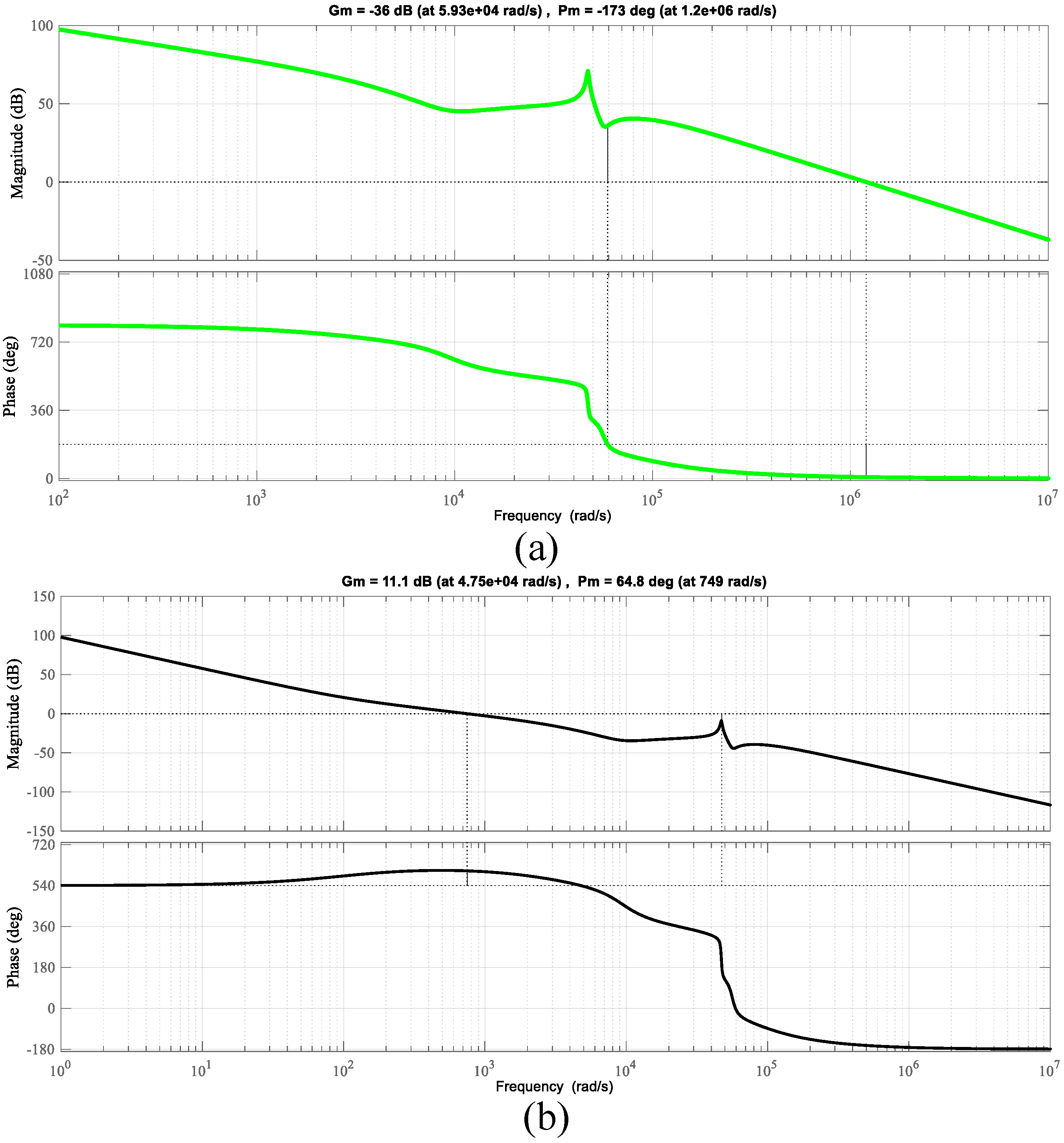
2.4. Voltage/Current Stresses of Semiconductor-Based Components

By expressing the average value of the inductor currents and capacitor voltages, the current/voltage of the semi-conductor-based components can be expressed as (3):
V S 1 = V D 1 = V i n 1 D , V S 2 = V i n ( 1 D ) 2 , V D 2 = D ( 2 D ) ( 1 D ) 2 V i n I S 1 = D ( 1 D ) 2 I o , I S 2 = I D 1 = D 1 D I o , I D 2 = 1 1 D I o

2.5. Current Ripple of Inductors and Voltage Ripple of Capacitors

The current ripple of the inductors is defined as the difference between the maximum and minimum value of the inductor current waveforms. According to the voltage–current relation of the inductors in the integral form, the simplified form of the current ripple can be defined based on the applied voltage of the inductor in one of the operation modes. Similarly, the voltage ripple can be defined as the difference between the maximum and minimum value of the voltage waveform. Based on the integral form of the voltage–current relation of the capacitors, the simplified form of the voltage ripple can be defined according to the crossing currents from the capacitor in one of the operation modes. The mathematical expression of the explained concepts is as (4):
Δ i L 1 = D V i n L 1 f s , Δ i L 2 = D V i n ( 1 D ) L 2 f s , Δ i L 3 = ( 1 D ) V o L 3 f s Δ v c 1 = D V o ( 1 D ) R C 1 f s , Δ v c 2 = D V o R C 2 f s , Δ v o = ( 1 D ) V o 8 C o f 2 s L 3

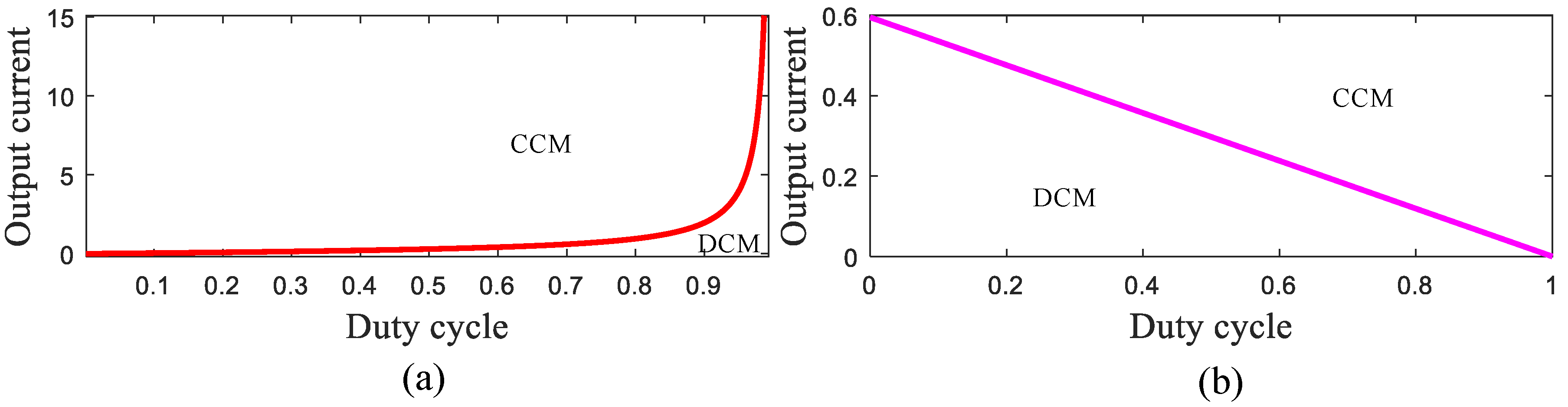
3. Discontinuous Conduction Mode

The inductor value affects the current ripple. In other words, a decrease in the inductor value increases the current ripple. A current ripple that is higher than twice the average current leads to DCM. Therefore, the minimum value of the inductors are expressed as (5):
L 1 ( 1 D ) 4 R 2 D ( 2 D ) f s , L 2 ( 1 D ) 2 R 2 D ( 2 D ) f s , L 3 ( 1 D ) R 2 f s ,
In addition to the inductor ripple current, the average value of the current also affects the operation mode. In other words, a lower average current that is lower than half of the current ripple, concludes the operation of the converter in DCM. In addition, the average current of the inductor depends on the average output current. Therefore, the operation region of the converter was extracted, as illustrated in Figure 3, based on the varying value of the duty cycle and the output current for both constant output/input voltage. The voltage gain of the converter has a different behavior in DCM. In other words, the ideal voltage gain of the converter depends on the duty cycle in CCM. However, such a concept is not true in DCM. The describing relations of the DCM voltage gain are as (6), where D, D1, & D2 represents the time-intervals that the switches are on, diodes are on, and all the semiconductors are off, respectively.
D + D 1 + D 2 = 1 , V o = V i n D ( D + 2 D 1 ) D 1 2

4. The Non-Ideal Mode

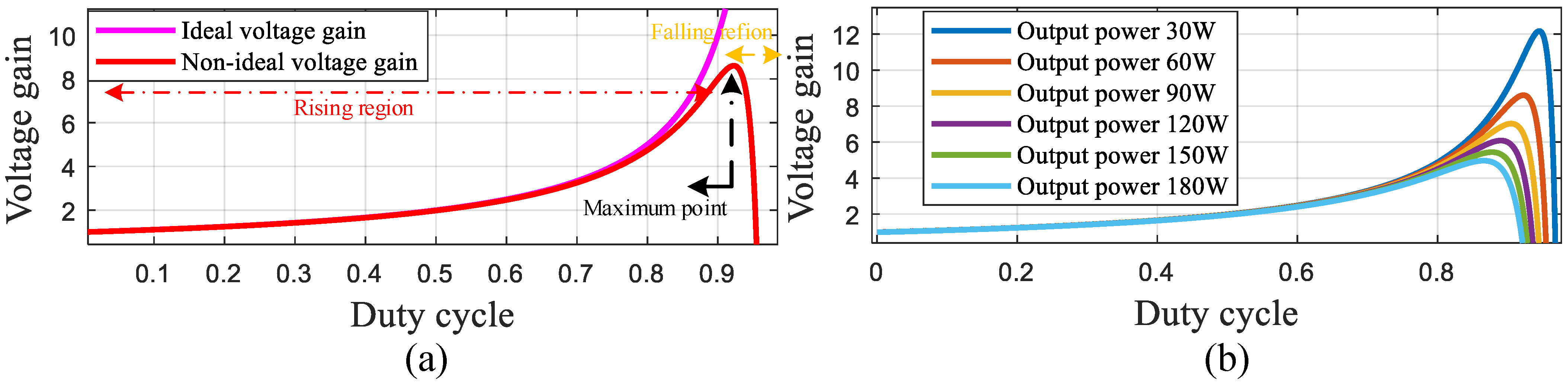
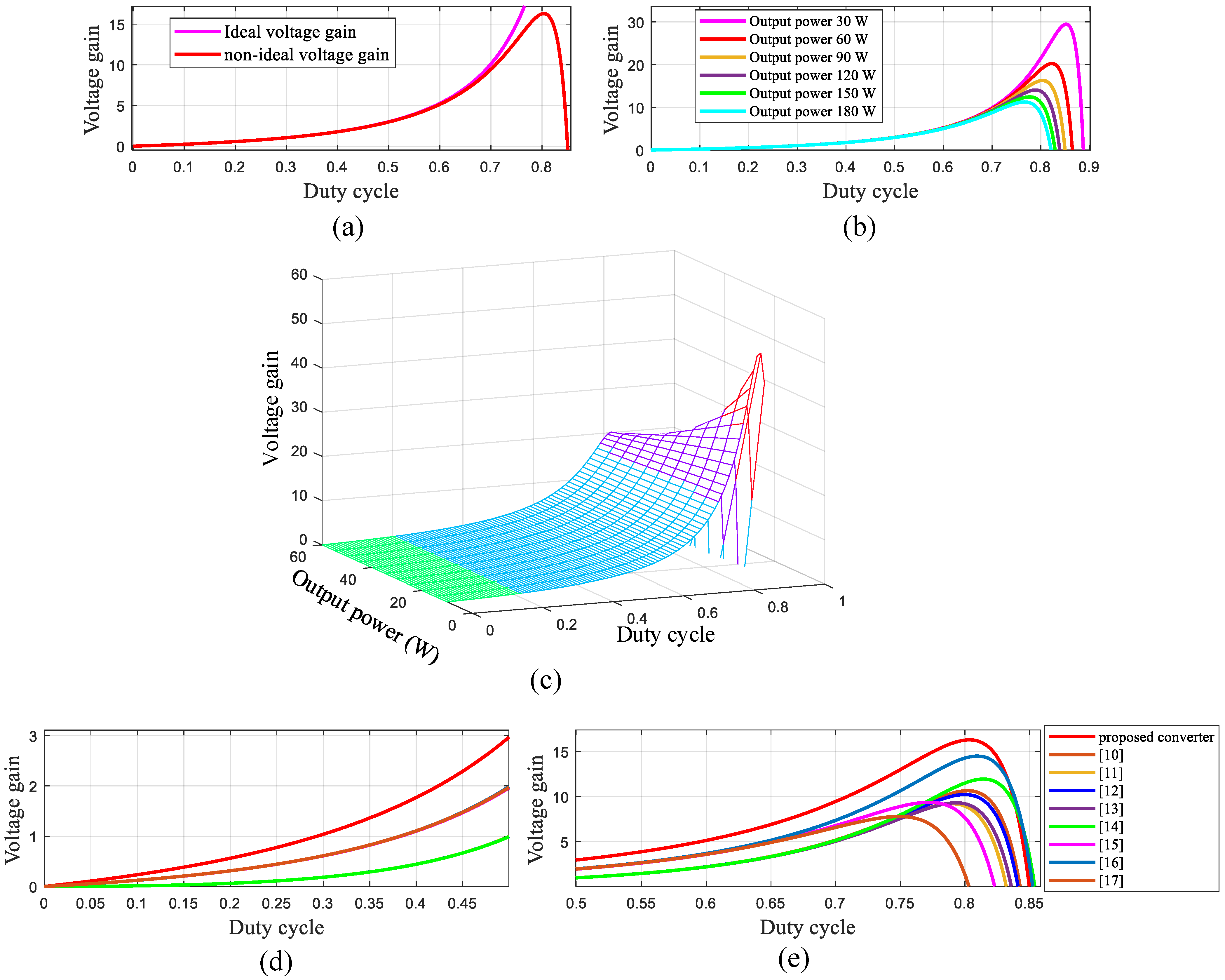
4.1. The Non-Ideal Voltage Gain
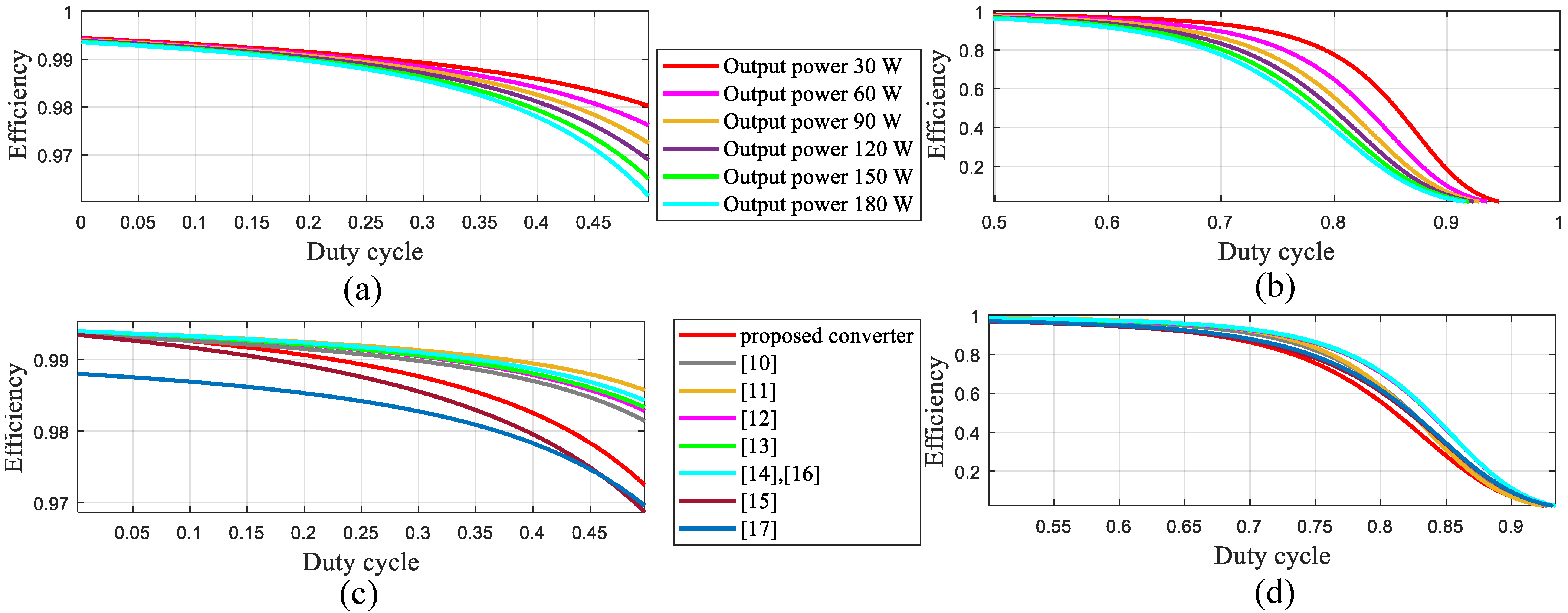
In the second section, the converter was investigated in the ideal mode. In other words, the expressed voltage gain was extracted by ignoring the resistance of the inductors ( r L ), and the dynamic resistance of the switches and diodes ( r S , r D ). However, the expressed voltage gain in the second section cannot clearly describe the prototype’s behavior. The voltage gain of the converter is expressed by the employment of the parasitic components, as (7):
V o V i n = D ( 2 D ) ( 1 D ) 2 G r L ( D ) G r S ( D ) G r D ( D ) G r L ( D ) = r L R 2 D 4 4 D 3 ( 1 D ) 5 , G r S ( D ) = r S R D 5 2 D 4 2 D 3 + 4 D 2 ( 1 D ) 6 , G r D ( D ) = r D R D 2 + 2 D ( 1 D ) 5
The difference of the voltage gain, in both ideal and non-ideal modes, is illustrated in Figure 4a. According to Equation (7), the parasitic components of the circuit elements, as well as the load, affect the voltage gain. It is worth noting that the parasitic components of the circuit elements refer to the quality of the used equipment. In addition, the load value refers to the output power. As seen in Figure 4b, the voltage gain of the non-ideal mode was plotted for different values of the output power. It can be understood that an increase in the output power decreases the maximum value of the voltage gain. In addition, an increase in the output power level shortens the rising interval of the voltage gain versus duty cycle. As presented in Figure 4c, the behavior of the voltage gain in a non-ideal mode was plotted for both the varying duty cycles and output power. It can be understood that the value of the maximum gain and its corresponding duty cycle increases as the output decreases. In Figure 4d,e, the voltage gain of the proposed topology is compared with [10,11,12,13,14,15,16,17] in the non-ideal mode of the converters. According to Figure 4d, while the duty cycle varies from 0 to 50 percent, the voltage gain of [10,11,12,13,14] varies from 0 to unity. The voltage gain of [15,16,17] varies from 0 to 2 in this interval and the voltage gain of the proposed converter varies from 0 to 3. In Figure 4e, where the duty cycle varies from 50 to 100, the voltage gain of the suggested converter varies from 3 to 16. Consequently, it can be deduced that this converter has a better and higher voltage gain in both ideal and non-ideal modes.

4.2. Efficiency

To obtain the converter efficiency, the conduction loss of inductors, switches, and diodes, and the frequency loss of the switches, are explained here. It is worth noting that the magnetic loss, hysteresis loss, eddy current loss, and frequency loss of the inductors were neglected. Moreover, the use of MKT-type capacitors, which have extremely low equivalent series resistors (ESRs), made it possible to neglect the conduction loss of capacitors. Additionally, the parasitic inductance of the circuit components store energy by currents and discharges as voltage spikes during the transient inactivation [7]. The conduction loss of inductors, switches, and diodes, and the frequency loss of the switches, are expressed as (8), respectively:
P L = r L 1 I 2 r m s 1 + r L 2 I 2 r m s 2 + r L 3 I 2 r m s 3 = r L 1 D 2 ( 2 D ) 2 ( 1 D ) 4 + r L 2 D 2 ( 1 D ) 4 + r L 3 P o R P S = r D S 1 I 2 S 1 , r m s + r D S 2 I 2 S 2 , r m s = r D S 1 D ( 1 D ) 2 + r D S 2 D ( 1 D ) 4 P o R P D = V D F 1 I D 1 + V D F 2 I D 2 V D F 1 D 1 D + V D F 2 1 1 D I o P S S = 1 2 ( I S 1 V S 1 t O F F 1 f s + I S 2 V S 2 t O F F 2 f s ) = t o f f 1 + t o f f 2 P o f s ( 1 D ) ( 2 D )
The expressed equations state is that the efficiency depends on the quality of the circuit components and output power. In Figure 5a,b, the efficiency graph is plotted for the different values of the output power for all values of the duty. According to Figure 5a, while the duty cycle varies from 0 to 50 percent, the efficiency of the converter is more than 96 percent for the considered output powers. Moreover, based on Figure 5b, while the duty cycle is lower than 70 percent, the efficiency is more than 80 percent for the considered output powers. By increasing the duty cycle to 72 percent, the efficiency becomes more than 80 percent only for output power levels of 30 to 90 W. In Figure 5c,d, the efficiency of the proposed topology and converters of [10,11,12,13,14,15,16,17] are compared. As seen in Figure 5c, the efficiency of the proposed converter is close to the other topologies—well above 97 percent—when the duty cycle varies from 0 to 50 percent. Based on Figure 5d, the efficiency of the proposed converter is approximately the same as the others, as the duty cycle varies from 50 percent to 75 percent.

5. Comparative Analysis with Other Topologies

In this section, different parameters are expressed for the recommended converter, besides the recently proposed converters. It is worth noting that the output voltage and input current were assumed as basic values for normalizing voltage/current stresses, respectively. Moreover, to calculate the different kinds of losses and voltage/current stress of semiconductors, a value of the duty cycle was used that concluded a three-time voltage gain in the mentioned topologies.

5.1. Different Kinds of Power Losses

In Table 1, the conduction loss of the inductors and switches is expressed and valued by the duty cycle that leads to the voltage gain of 3. The corresponding value of the duty cycle is reported in Table 2. It can be understood that the conduction loss of the inductors in the suggested converter is lower than [11,12,13,14,15,17]. In addition, the conduction loss of the switch in this converter is lower than all of the other converters, except [15,16].
In Table 2, the switching loss of the switch, the conduction loss of the diodes, the corresponding value of the duty cycle, and concluded efficiency are reported. It can be understood that the proposed converter has achieved the lowest value in comparison with [10,11,12,13,14,15,16,17]. In addition, the conduction loss of the diode is only lower than [15,17]. Moreover, the suggested converter uses the lowest value of the duty cycle to provide the voltage gain of 3. In the last column of the second table, the efficiency is reported. As reported, the suggested converter has the highest efficiency among [10,11,12,13,14,15,17]. It is worth noting that the difference between the efficiency of the proposed converter and [16] is 0.5 percent.

5.2. The Comparison of the Current/Voltage Stress of the Switches and Diodes at the Operating Point

In Table 3, the normalized voltage stress of switches and diodes is valued by a percentage of the duty cycle, which provides the voltage gain of 3. Based on the mentioned table, the first switch and diode of this converter have achieved the lowest values among [10,11,12,13,14,15,16,17]. The voltage stress of the second switch is lower than [10,11,13,14,15,16]. However, the voltage stress of the second diode of this converter is more than the others.
In Table 4, the current stress of the switches and diodes are compared. As can be seen, the current stress of the first switch is lower than [10,11,12,13,14,15,17]. In addition, the current stress of the second switch and the first diode are the lowest values among [10,11,12,13,14,15,16,17]. However, the current stress of the second diode is more than the others. It is worth noting that interested readers can use the reported normalized values of the current/voltage stresses in Table 4 and Table 5 to find the behavior of the normalized values for different values of the duty cycle.

5.3. The Comparison of the Component Numbers and Continuity of Input/Output Currents

In Table 5, the number of circuit components and the continuity of the input/output currents are compared among the proposed topology and suggested topologies of [10,11,12,13,14,15,16,17]. The number of inductors and capacitors is the same in the suggested topology and converters of [10,12,14,15,16]. In addition, the number of switches and diodes is the same in all converters. The input current of the suggested topology and proposed converters of [11,12,14,15,16] are continuous. In addition, the output current of the suggested design is continuous, the same as [11,14].

6. Simulation Results

To verify the findings of the second section, the simulation results are discussed here. To find the suitable values of the inductors and capacitors, some parameters need to be considered. The voltage and current values need to follow the safety requirements and equipment limits. Therefore, the input voltage and output current have exceeded 30 V and 1 A, respectively. Due to the frequency limits of the inductor wire, switching frequency was set to 100 kHz. Moreover, according to the power quality considerations, the current ripple of the inductors and voltage ripple of the capacitors were considered 30 and 5 percent, respectively. The average value of the inductor currents and capacitor voltages are calculated by Equation (3). Consequently, the average inductor current and average capacitor voltage are expressed as (9).
I L 1 = 3 A , I L 2 = I L 3 = 1 A , V C 1 = 60 V , V C 2 = 120 V , V O = 90 V
Based on the calculated values in (9), and the expressed relations of (4), the inductors and capacitors are expressed as (10):
L 1 = 160 μ H , L 2 = 1000 μ H , L 3 = 1500 μ H , C 1 = 3.34 μ F , C 2 = 0.83 μ F , C o = 0.083 μ F
The simulation results were extracted by PLECS software. The voltage/current waveforms of all circuit components are presented in Figure 6. According to Figure 6a–f, the average value of the inductor current and capacitor voltage is as (11):
I L 1 = 3 A , I L 2 = I L 3 = 1 A , V C 1 = 59.5 V , V C 2 = 120 V , V O = 90 V
A comparison between (11) and (9) confirms their compatibility. In addition, based on the extracted Figure 6g–l, the average voltage of the inductors and average current of the capacitors is zero and the extracted results are compatible with the voltage/current second balance. In Figure 6m–p, the current waveforms of semiconductors are presented. It is worth noting that the switches are activated synchronously. Moreover, during the activation of diodes, the switches are OFF. These concepts are compatible with the theoretical descriptions of the second section. In Figure 6q–t, the voltage waveforms of the semiconductors are presented. It can be understood that the voltage of the first capacitor was applied to the first switch and diode. Moreover, the applied voltage to the second switch is the second capacitor voltage, which is compatible with the extracted result in Figure 6r. Furthermore, the applied voltage to the second diode is the sum of the first and second capacitors, which is compatible with the extracted outcome.

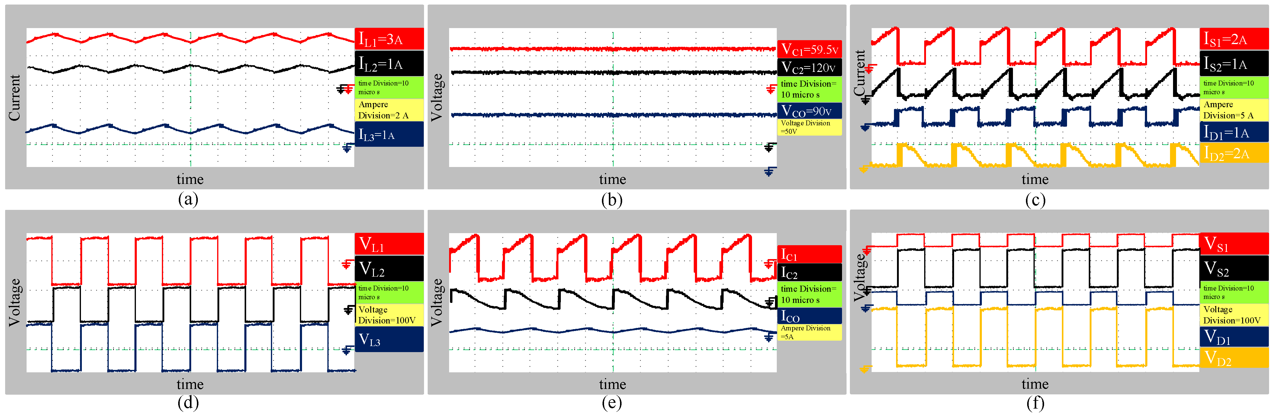
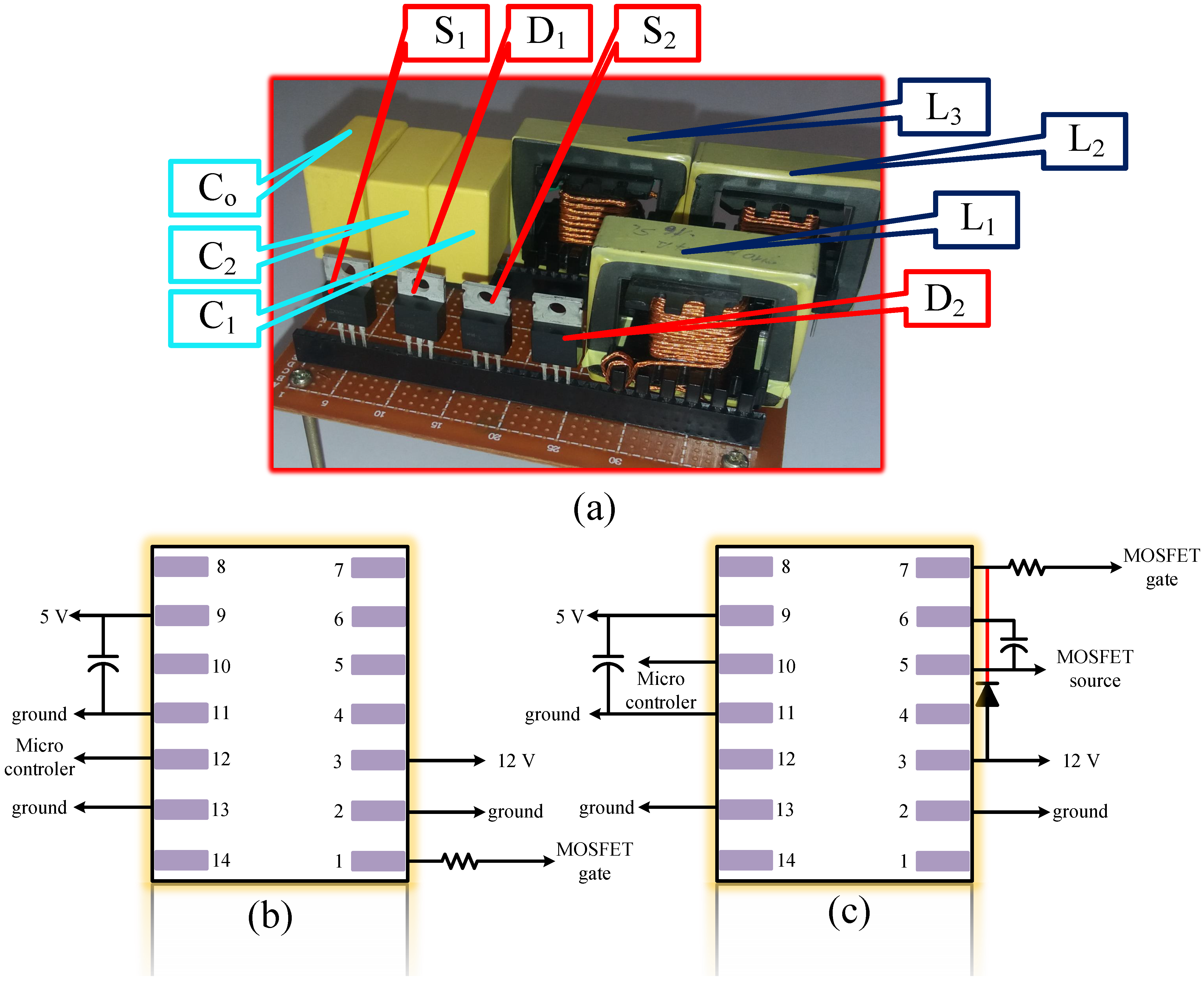
7. Experimental Results

In line with the simulation results, the current/voltage waveforms of all circuit components were extracted. Similar to the simulation results, the minimum values of the capacitor and inductors of the prototype follow the calculations of (10). Moreover, metallized polyester film capacitors with low ESR were used. In addition, for the inductor windings, litz wires were used. Moreover, IRF540 and 2015OCT were used as the MOSFET and diode in the prototype. Furthermore, IRF2110 was used as the driver of the MOSFET. The experimental results are presented in Figure 7. According to Figure 7a, the average current of the first, second, and third inductors is 3 A, 1 A, and 1 A, respectively. Moreover, based on Figure 7d, the voltage of the inductors is compatible with volt-second balance. It is worth noting that, in Figure 7b, the voltage waveform of the capacitors are illustrated. Additionally, the average value of the voltage is 59.5 V, 120 V, and 90 V for the first to third capacitors, respectively. Moreover, the charge-second balance can be understood from Figure 7e, due to the zero average value of the presented current waveforms. In Figure 7c,f, the current waveforms and voltage waveforms of the semiconductors are presented, respectively. According to Figure 7c, the operation of the semiconductor takes place asynchronously, which is compatible with the theoretical analysis of the paper, as well as the simulation results. Moreover, the applied voltages to the semiconductors during their OFF mode is compatible with the simulation results and the theoretical equations. It is worth noting that the prototype is shown in Figure 8a. Moreover, the detailed information of the MOSFET drivers are illustrated in Figure 8b,c for low-side and high-side switches, respectively. Additionally, other comparisons based on the experimental results are presented in Figure 9. In Figure 9a,b, the diagram of the non-ideal voltage gain is compared with the extracted results of the experiment for 90 W output power, 30 V input voltage, and varying duty cycles. It can be understood that, while the duty cycle varies from 20 to 50 percent, according to Figure 9a, the theoretical and experimental voltage gains will perfectly match. The same concept is true for the duty cycles ranging between 50 and 70 percent, as per Figure 9, but there is a difference between the theory and experiments in duty cycles greater than 70 percent, which was predictable due to the parasitic effects. In Figure 9c,d, the efficiency of the converter is compared based on the theoretical analysis and experiments. It can be understood that while the duty cycle varies from 20 percent to 50 percent in Figure 9c, the differences of the curves increase from 2 percent to 3 percent. Moreover, while the percentage of the duty cycle becomes 50 percent, the extracted efficiency from the theory and experiment is 97 percent and 93.6 percent, respectively. Furthermore, according to Figure 9d, the efficiency of the converter is higher than 80 percent for the percentage of the duty cycles lower than 71. However, this value is 73 percent in the theoretical result. Typically, the efficiency of the power converter declines as the duty cycle of the switch increases, due to the increase of the power loss over the components. However, it should be noted that the practical voltage gain in a transformer-less topology would not normally exhibit ultra-high voltage gains, due to the parasitic effect, which confirms the efficiency yield of over 80 percent for the practical gains in Figure 9. We should note that the experimental efficiency and different losses are expressed for the operating point in Figure 9e,f. The diode and inductor losses are the same at the operating point according to Figure 9f. Moreover, according to this figure, the switch loss is lower than the diode and inductor losses. In Figure 9g, the efficiency of the converter is extracted for the different output powers from the theory and experiment, while the duty cycle is 50 percent, and the output voltage is 90 V.

8. Conclusions

In this article, a high step-up DC–DC converter was proposed. The proposed converter was based on the Cuk converter. Therefore, the continuity of the input current was maintained. This feature makes this converter suitable for renewable energy applications. Moreover, the ideal model of the proposed converter was studied and explained in CCM and DCM. The average voltage of the capacitors, the voltage gain, the boundary value of the inductors, and the CCM and DCM operation regions were studied. The relation of the non-ideal voltage ratio was extracted, which was then compared with the practical voltage ratio to validate its combustibility. Furthermore, the improvements of the proposed converter, in comparison with the conventional Cuk and the other converters, were discussed; it was deduced that the proposed converter has a higher voltage ratio by the lower value of the duty cycle. The mathematical equations of the efficiency and different power losses were expressed. Therefore, the advantages of the proposed converter were discussed in various aspects. Finally, the simulation and the experimental results were delivered and compared with the design assumptions based on the theoretical analysis. Finally, the compatibility of the simulation and experimental results with the theoretical relations validated the correctness of the mathematical analysis.

Author Contributions

Conceptualization, H.G. and S.A.G.; methodology, H.G., S.A.G. and D.S.; validation, H.G.; formal analysis, H.G.; resources, E.A.; writing—original draft preparation, H.G.; writing—review and editing, S.A.G., D.S. and E.A.; supervision, S.A.G., E.A. and D.S.; funding acquisition, E.A. and D.S. All authors have read and agreed to the published version of the manuscript.

Funding

This research received no external funding.

Conflicts of Interest

The authors declare no conflict of interest.

Appendix A

The state equations of the proposed converter are as (A1).
L 1 d < i L 1 > d t = V i n + d < v c 1 > ( 1 d ) < v c 2 > L 2 d < i L 2 > d t = d < v c 1 > + ( 1 d ) < v c 2 > L 3 d < i L 3 > d t = d < v c 1 + v c 2 > < v o > c 1 d < v c 1 > d t = < i L 2 > d < i L 1 + i L 3 > c 2 d < v c 2 > d t = d < i L 3 > + ( 1 d ) < i L 1 i L 2 > c o d < v o > d t = < i L 3 > < v o > R
The required assumptions and neglecting are as (A2).
i L 1 = i ^ L 1 + I L 1 , i L 2 = i ^ L 2 + I L 2 , i L 3 = i ^ L 3 + I L 3 , v c 1 = v ^ c 1 + V c 1 , v c 2 = v ^ c 2 + V c 2 , v o = v ^ o + V o i ^ L 1 < < I L 1 , i ^ L 2 < < I L 2 , i ^ L 3 < < I L 3 , v ^ c 1 < < V c 1 , v ^ c 2 < < V c 2 , v ^ o < < V o
The space state equations based on the state matrices are as (A3).
x ˙ = A x + B u ,   y = C x
The mentioned matrices are as:
d i ^ L 1 d t d i ^ L 2 d t d i ^ L 3 d t d v ^ C 1 d t d v ^ C 2 d t d v ^ C o d t = 0 0 0 D L 1 D 1 L 1 0 0 0 0 D L 2 1 D L 2 0 D C 1 1 C 1 D C 1 0 0 0 1 D C 2 1 D C 2 D C 2 0 0 0 0 0 1 C o 0 0 1 R C o x + b 11 b 12 b 13 b 14 d ^ , y = 0 0 0 0 0 1 t d
Based on the expressed relations, the bode diagram of the converter is illustrated in Figure A1 for both before/after compensating. Additionally, gain and phase margins for both mentioned modes are expressed as (A4) and (A5).
Gm = −36 dB, Pm = 173 deg
Gm = 11.1 dB, Pm = 64.8 deg
The appropriate compensator for the mentioned converter was calculated by MATLAB as (A6).
0.010318 * 1 + 0.0099 s s
Figure A1. The bode diagram: (a) before compensating; (b) after compensating.
Energies 14 06975 g0a1

References

  1. Li, W.; Lv, X.; Deng, Y.; Liu, J.; He, X. A Review of Non-Isolated High Step-Up DC/DC Converters in Renewable Energy Applications. In Proceedings of the 2009 Twenty-Fourth Annual IEEE Applied Power Electronics Conference and Exposition, Washington, DC, USA, 15–19 February 2009; pp. 364–369. [Google Scholar]
  2. Marjani, J.; Imani, A.; Hekmati, A.; Afjei, E. A new dual output DC–DC converter based on SEPIC and Cuk converters. In Proceedings of the 2016 International Symposium on Power Electronics, Electrical Drives, Automation and Motion (SPEEDAM), Capri, Italy, 22–24 June 2016; pp. 946–950. [Google Scholar]
  3. Gopi, R.R.; Sreejith, S. Converter topologies in photovoltaic applications—A review. Renew. Sustain. Energy Rev. 2018, 94, 1–14. [Google Scholar] [CrossRef]
  4. Amir, A.; Amir, A.; Che, H.S.; Elkhateb, A.; Abd Rahim, N. Comparative analysis of high voltage gain DC–DC converter topologies for photovoltaic systems. Renew. Energy 2019, 136, 1147–1163. [Google Scholar] [CrossRef] [Green Version]
  5. Tewari, N.; Sreedevi, V. A novel single switch dc-dc converter with high voltage gain capability for solar PV based power generation systems. Sol. Energy 2018, 171, 466–477. [Google Scholar] [CrossRef]
  6. Revathi, B.S.; Prabhakar, M. Non isolated high gain DC–DC converter topologies for PV applications—A comprehensive review. Renew. Sustain. Energy Rev. 2016, 66, 920–933. [Google Scholar] [CrossRef]
  7. Liu, T.; Wong, T.T.Y.; Shen, Z.J. A Survey on Switching Oscillations in Power Converters. IEEE J. Emerg. Sel. Top. Power Electron. 2020, 8, 893–908. [Google Scholar] [CrossRef]
  8. Górecki, P.; Górecki, K. Analysis of the Usefulness Range of the Averaged Electrothermal Model of a Diode–Transistor Switch to Compute the Characteristics of the Boost Converter. Energies 2021, 14, 154. [Google Scholar] [CrossRef]
  9. Forouzesh, M.; Siwakoti, Y.P.; Gorji, S.A.; Blaabjerg, F.; Lehman, B. Step-Up DC–DC Converters: A Comprehensive Review of Voltage-Boosting Techniques, Topologies, and Applications. IEEE Trans. Power Electron. 2017, 32, 9143–9178. [Google Scholar] [CrossRef]
  10. Miao, S.; Wang, F.; Ma, X. A New Transformerless Buck-Boost Converter With Positive Output Voltage. IEEE Trans. Ind. Electron. 2016, 63, 2965–2975. [Google Scholar] [CrossRef]
  11. Sarikhani, A.; Allahverdinejad, B.; Hamzeh, M.; Afjei, E. A continuous input and output current quadratic buck-boost converter with positive output voltage for photovoltaic applications. Sol. Energy 2019, 188, 19–27. [Google Scholar] [CrossRef]
  12. Gholizadeh, H.; Salehi, M.; Rafiee, Z.; Afjei, E.; Hamzeh, M. A Transformer less Quadratic Buck-Boost Converter with Wide Range of Output Voltage and Low Switch Stresses. In Proceedings of the 2020 11th Power Electronics, Drive Systems, and Technologies Conference (PEDSTC), Tehran, Iran, 4–6 February 2020; pp. 1–6. [Google Scholar]
  13. Babazadeh, Y.; Babaei, E.; Sabahi, M. A New Non-Isolated Buck-Boost Converter with High Voltage Gain and Positive Output Voltage for Renewable Energy Applications. In Proceedings of the 2019 10th International Power Electronics, Drive Systems and Technologies Conference (PEDSTC), Shiraz, Iran, 12–14 February 2019; pp. 201–206. [Google Scholar]
  14. Gholizadeh, H.; Sarikhani, A.; Hamzeh, M. A Transformerless Quadratic Buck-Boost Converter Suitable for Renewable Applications. In Proceedings of the 2019 10th International Power Electronics, Drive Systems and Technologies Conference (PEDSTC), Shiraz, Iran, 12–14 February 2019; pp. 470–474. [Google Scholar]
  15. Totonchi, N.; Gholizadeh, H.; Afjei, E.; Hamzeh, M. A Novel Transformer less High Gain DC–DC Converter with Continuous Input Current and Suitable for Photo Voltaic Panels. In Proceedings of the 2020 11th Power Electronics, Drive Systems, and Technologies Conference (PEDSTC), Tehran, Iran, 4–6 February 2020; pp. 1–6. [Google Scholar]
  16. Gholizadeh, H.; Aboufazeli, S.; Rafiee, Z.; Afjei, E.; Hamzeh, M. A Non-Isolated High Gain DC–DC Converters with Positive Output Voltage and Reduced Current Stresses. In Proceedings of the 2020 11th Power Electronics, Drive Systems, and Technologies Conference (PEDSTC), Tehran, Iran, 4–6 February 2020; pp. 1–6. [Google Scholar]
  17. Garcia-Vite, P.M.; Soriano-Rangel, C.A.; Rosas-Caro, J.C.; Mancilla-David, F. A DC–DC converter with quadratic gain and input current ripple cancelation at a selectable duty cycle. Renew. Energy 2017, 101, 431–436. [Google Scholar] [CrossRef]
Figure 1. Ideal and non-ideal voltage gains of the boost converter: (a) limits of the boost converter’s voltage gain in non-ideal mode, (b) the behavior of the non-ideal voltage gain for different output powers.
Energies 14 06975 g001
Figure 2. (a) Cuk converter and how it was modified; (b) the recommended design; (c) the procedure of its creation from the recommended structure and Cuk converter; (d) the equivalent circuit of the first mode; and (e) equivalent circuit of the second mode.
Energies 14 06975 g002
Figure 3. Operational region of the converter in CCM and DCM, while the frequency is 100 kHz, the last inductor is 1500 μ H , and (a) the output voltage is constant (90 V), (b) the input voltage is constant (30 V).
Energies 14 06975 g003
Figure 4. (a) Comparison of ideal and non-ideal voltage gain; (b) comparison of non-ideal voltage gain for different output powers; (c) behavior of the voltage gain with respect to the varying duty cycles and output power; (d) comparison of the voltage gain of the high gain converter for the varying duty cycles from 0 to 50 percent; (e) comparison of the voltage gain of high gain converter for the varying duty cycles from 50 to 85 percent.
Energies 14 06975 g004
Figure 5. (a) Efficiency of the converter for different output powers and the varying duty cycles from 0 to 50 percent; (b) efficiency of the converter for different output powers and the varying duty cycles from 50 to 100 percent; (c) comparison of the efficiencies of high gain converters for varying duty cycles from 0 to 50 percent; (d) comparison of the efficiencies of high gain converters for varying duty cycles from 50 to 100 percent.
Energies 14 06975 g005
Figure 6. (a) First inductor current; (b) second inductor current; (c) third inductor current; (d) first capacitor voltage; (e) second capacitor voltage; (f) output capacitor voltage; (g) first inductor voltage; (h) second inductor voltage; (i) third inductor voltage; (j) first capacitor current; (k) second capacitor current; (l) output capacitor current; (m) first switch current; (n) second switch current; (o) first diode current; (p) second diode current; (q) first switch voltage; (r) second switch voltage; (s) first diode voltage; (t) second diode voltage.
Energies 14 06975 g006
Figure 7. The experimental results: (a) inductors current; (b) capacitors voltage; (c) semiconductors current; (d) inductors voltage; (e) capacitors current; (f) semiconductors voltage.
Energies 14 06975 g007
Figure 8. (a) The prototype; (b) driver of the low side switch; (c) driver of the high-side switch.
Energies 14 06975 g008
Figure 9. Theoretical analysis vs. experiments: (a) the comparison of the theoretical and experimental voltage gain, while the duty cycle varies from 0 to 50 percent; (b) the comparison of the theoretical and experimental voltage gain, while the duty cycle varies from 50 to 100 percent; (c) the comparison of the theoretical and experimental efficiency, while the duty cycle varies from 0 to 50 percent; (d) the comparison of the theoretical and experimental efficiency, while the duty cycle varies from 50 to 100 percent; (e) pie chart of the efficiency and losses; (f) loss break down; (g) comparison of the theoretical and experimental efficiency for varying output power, from 30 to 180 W.
Energies 14 06975 g009
Table 1. Comparison of power loss of inductors and switches (conduction) as the voltage gain ratio equals 3.
Inductors Loss (W)Switches Conduction Loss (W)
proposed converters P o r L R 2 D 4 8 D 3 + 11 D 2 4 D + 1 ( 1 D ) 4 = 0.63 P o r S R D 3 2 D 2 + 2 D ( 1 D ) 4 = 0.45
[10] P o r L R 2 D 4 6 D 3 + 8 D 2 4 D + 1 ( 1 D ) 4 = 0.5 P o r S R 2 D 3 2 D 2 + D ( 1 D ) 4 = 0.8
[11] P o r L R 3 D 4 5 D 3 + 7 D 2 4 D + 1 ( 1 D ) 4 = 1.15 P o r S R 5 D 3 4 D 2 + D ( 1 D ) 4 = 0.7
[12] P o r L R D 4 2 D 3 + 3 D 2 2 D + 1 ( 1 D ) 4 = 1.41 P o r S R 2 D 3 2 D 2 + D ( 1 D ) 4 = 0.8
[13] P o r L R 2 D 2 2 D + 1 ( 1 D ) 4 = 1.28 P o r S R 2 D 3 2 D 2 + D ( 1 D ) 4 = 0.8
[14] P o r L R 2 D 4 6 D 3 + 8 D 2 4 D + 1 ( 1 D ) 4 = 1.12 P o r S R 2 D 3 2 D 2 + D ( 1 D ) 4 = 0.8
[15] P o r L R 3 D 2 4 D + 2 ( 1 D ) 4 = 0.91 P o r S R 2 D 3 6 D 2 + 5 D ( 1 D ) 4 = 0.8
[16] P o r L R 2 D 4 6 D 3 + 8 D 2 4 D + 1 ( 1 D ) 4 = 0.55 P o r S R 2 D 3 2 D 2 + D ( 1 D ) 4 = 0.4
[17] P o r L R D 2 2 D + 2 ( 1 D ) 4 = 1.56 P o r S R D 3 2 D 2 + 2 D ( 1 D ) 4 = 0.88
Table 2. Comparison of power loss in switches (switching) and diodes as the voltage gain ratio equals 3.
Switching Loss of Switches (W)Diodes Loss (W)Duty Cycle η
proposed converters f s P o t o f f ( 1 D ) ( 2 D ) = 0.013 V D F I o ( 1 + D ) 1 D = 1.5 0.597.2
[10] f s P o t o f f 1 D = 0.027 V D F I o 1 D = 1.35 0.6397.1
[11] f s P o t o f f D ( 1 D ) 2 = 0.046 V D F I o 1 D = 1.35 0.6396.5
[12] f s P o t o f f ( 1 + D ) 1 D = 0.044 V D F I o 1 D = 1.35 0.6396.1
[13] f s P o t o f f 1 D = 0.027 V D F I o 1 D = 1.35 0.6396.3
[14] f s P o t o f f 1 D = 0.027 V D F I o 1 D = 1.35 0.6396.4
[15] f s P o t o f f ( 1 + D ) 1 D = 0.036 V D F I o ( 1 + D ) 1 D = 1.82 0.5796.6
[16] f s P o t o f f ( 1 + D ) 1 D = 0.036 V D F I o 1 D = 1.15 0.5797.7
[17] f s P o t o f f ( 1 + D ) 1 D = 0.036 V D F I o ( 2 D ) 1 D = 1.66 0.5795.6
Table 3. Comparison of the normalized voltage stress of semiconductors as the voltage gain ratio equals 3.
V S 1 V O V S 2 V O V D 1 V O V D 2 V O D
proposed converter 1 D D ( 2 D ) = 0.66 1 D ( 2 D ) = 1.32 1 D D ( 2 D ) = 0.66 1 D = 2 0.5
[12] 1 D D 2 = 0.821 1 D D 2 = 0.82 1 D = 1.60.63
[10] 1 D D 2 = 0.82 1 D = 1.6 1 D D 2 = 0.82 1 D = 1.60.63
[11] 1 D 2 = 2.56 1 D = 1.6 1 D D 2 = 0.82 1 D = 1.60.63
[13] 1 D D 2 = 0.82 1 D = 1.6 1 D D 2 = 0.82 1 D = 1.60.63
[14] 1 D D 2 = 0.82 1 D = 1.6 1 D D 2 = 0.82 1 D = 1.60.63
[15] 1 D D = 0.75 2 D 1 D = 0.24 1 D D = 0.7510.57
[16] 1 D D = 0.75 1 D = 1.75 1 D D = 0.75 1 D = 1.750.57
[17] 1 D D = 0.751 1 D D = 0.7510.57
Table 4. Comparison of the normalized current stress of semiconductors as the voltage gain ratio equals 3.
I S 1 I in I S 2 I in I D 1 I in I D 2 I in D V o V in
proposed converter 1 2 D = 0.66 1 D 2 D = 0.33 1 D 2 D = 0.33 1 D D ( 2 D ) = 0.66 0.5 D ( 2 D ) ( 1 D ) 2 = 3
[10]1 1 D D = 0.59 1 D D = 0.59 1 D D 2 = 0.330.63 D 1 D 2 = 3
[11]1 1 D D = 0.59 1 D D = 0.59 1 D D 2 = 0.330.63 D 1 D 2 = 3
[12]1 2 D 1 D = 0.41 2 D 1 D = 0.59 1 D D 2 = 0.330.63 D 1 D 2 = 3
[13]1 1 D D = 0.59 1 D D = 0.59 1 D D 2 = 0.330.63 D 1 D 2 = 3
[14]1 1 D D = 0.59 1 D D = 0.59 1 D D 2 = 0.330.63 D 1 D 2 = 3
[15] 2 D = 1.43 1 D = 0.43 1 D D = 0.75 ( 1 D ) 2 D = 0.330.57 D ( 1 D ) 2 = 3
[16]D = 0.57 1 D = 0.431-D = 0.43 ( 1 D ) 2 D = 0.330.57 D ( 1 D ) 2 = 3
[17]1 1 D = 0.57 1 D D = 0.75 ( 1 D ) 2 D = 0.330.57 D ( 1 D ) 2 = 3
Table 5. Comparison of component numbers and voltage gain.
No. LNo. CNo. SNo. DTotalInput CurrentOutput CurrentVoltage Gain
proposed332210ContinuousContinuous D 1 D 2
[10]22228DiscontinuousDiscontinuous D 1 D 2
[11]332210ContinuousContinuous D 1 D 2
[12]332210ContinuousDiscontinuous D 1 D 2
[13]22228DiscontinuousDiscontinuous D 1 D 2
[14]332210ContinuousContinuous D 1 D 2
[15]332210ContinuousDiscontinuous D ( 1 D ) 2
[16]332210ContinuousDiscontinuous D ( 1 D ) 2
[17]22228ContinuousDiscontinuous D ( 1 D ) 2
Publisher’s Note: MDPI stays neutral with regard to jurisdictional claims in published maps and institutional affiliations.

