1. Introduction
Insulated Gate Bipolar Transistors (IGBTs) are one of the most important components in medium and high power converters. They are commonly used in traction systems [
1,
2], pulsed power supplies [
3,
4,
5], HVDC circuit breakers [
6,
7,
8], and solid-state transformers [
9,
10]. IGBTs and capacitors are the components with 34% failure rates in the power converters [
11,
12,
13]. Short Circuit Faults (SCFs) are specially important as a frequent failure modes in the IGBT operation. There are several further factors that may break the device in particular cases; however, IGBT can withstand the SCF condition for a limited time, e.g., IGBTs can survive 10
of SCF condition until it reaches thermal runaway [
14,
15]. Among serious failure modes during SCF condition, we can name latch-up [
16], gate oscillation [
17,
18], self-turn off [
19], thermal run away during the turn-off state [
20,
21], Negative Differential Resistance (NDR) [
22,
23], and Metal–Oxide–Semiconductor Field-Effect Transistor (MOSFET) mode [
24]. Toward enhancing the reliability of IGBT devices, there have been several attempts in the literature.
The latch-up process occurs when the parasitic thyristor of the device is activated, and SCF current limiting of the IGBT malfunctions immediately. For latch-up, modifications in the structure of IGBTs are proposed in [
25], which has been applied in newer generations of IGBTs. For the modern IGBTs, therefore, the advanced designs provide a homogeneously SCF current sharing between the device cells, and hence, less sensitivity to latch-up failure has been obtained. In the gate-oscillation, leading to gate-oxide breakdown, both gate circuit elements and structural factors play important roles, and specific design and implementation for gate-oscillations mitigation are required [
26]. Structural modifications are also proposed for preventing self-turn-off and MOSFET modes [
27]. In the NDR condition, the SCF current flows unevenly through the IGBT in the turning-off process, which results in the current filament. Therefore, structural parameters of IGBTs, such as temperature dependency of device bipolar current gain (
) and the turning-off speed of the device, are the main origins of this mode [
28]. The thermal runaway in the turn-off state is a major challenge for the low-power IGBTs. In this failure mode, the device can withstand the SCF until 50∼100
after the SCF removal owing to the high leakage current. Considering the above discussion, limiting the SCF energy can be an effective approach for protecting the switch during this failure modes [
20,
29].
Besides the aforementioned, there are several efforts for protecting the IGBTs during SCF by shortening the SCF time interval with the general aim to minimize the SCF time and avoid the thermal runaway. In [
30,
31], de-saturation is proposed as an effective protection approach. In this technique, the collector-emitter voltage of the IGBT is monitored after the turn-on command to be negligible or not. In the SCF condition, this value is high and perceived as an indicator of device operation in its active region, and the IGBT must be turned off to terminate the SCF. The main drawback though is the mandatory blanking time (1∼5
) between sensing the fault and resolving it [
32] due to some intrinsic differences, such as the gate threshold voltage (
), input capacitance (
), and transconductance (
), resulting in different transient time intervals [
31]. The second protection approach is based on the device current rate of change (
di/dt) by sensing the Kelvin inductor voltage [
33,
34]. This approach has fast response in fault detection condition and is just suitable for the packages with visible Kelvin inductances. The third approach directly senses the collector current using shunts or current sensors [
14,
35]. In this approach, the observed current is filtered to avoid detection circuit malfunctioning subject to the noise and existing leakage inductance of the path, where the delay is unavoidable.
Overall, the existing protection strategies do not consider IGBTs failure modes during SCF condition and introduce delay. By limiting the SCF current, temporary SCF conditions like vacuum arcs can be omitted [
6,
7] in less than several
if the SCF current is accurately limited. The IGBT, however, must be turned off, and after fault removal and protection resetting, IGBT is turned on again for normal operation after a comparatively long period.
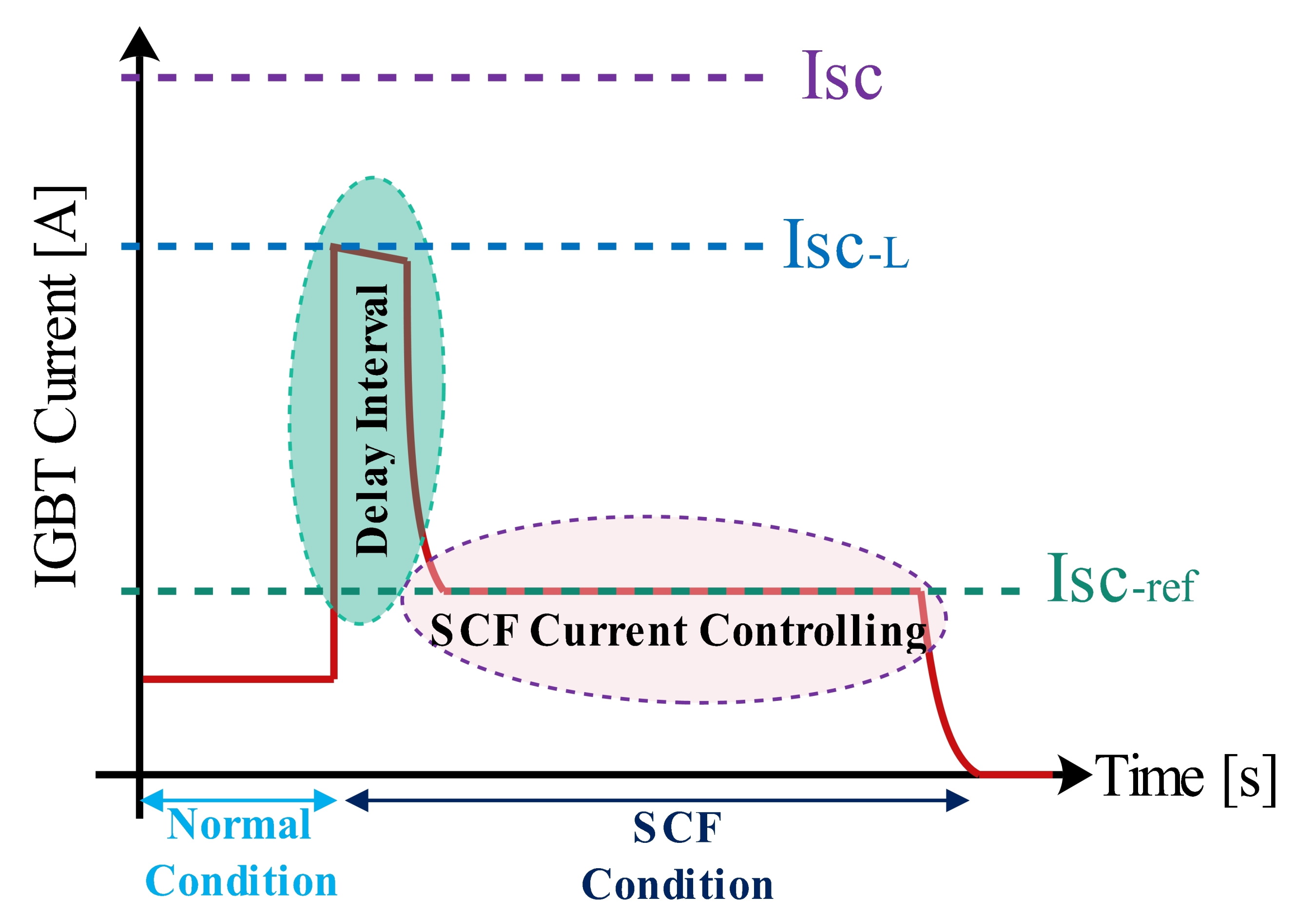
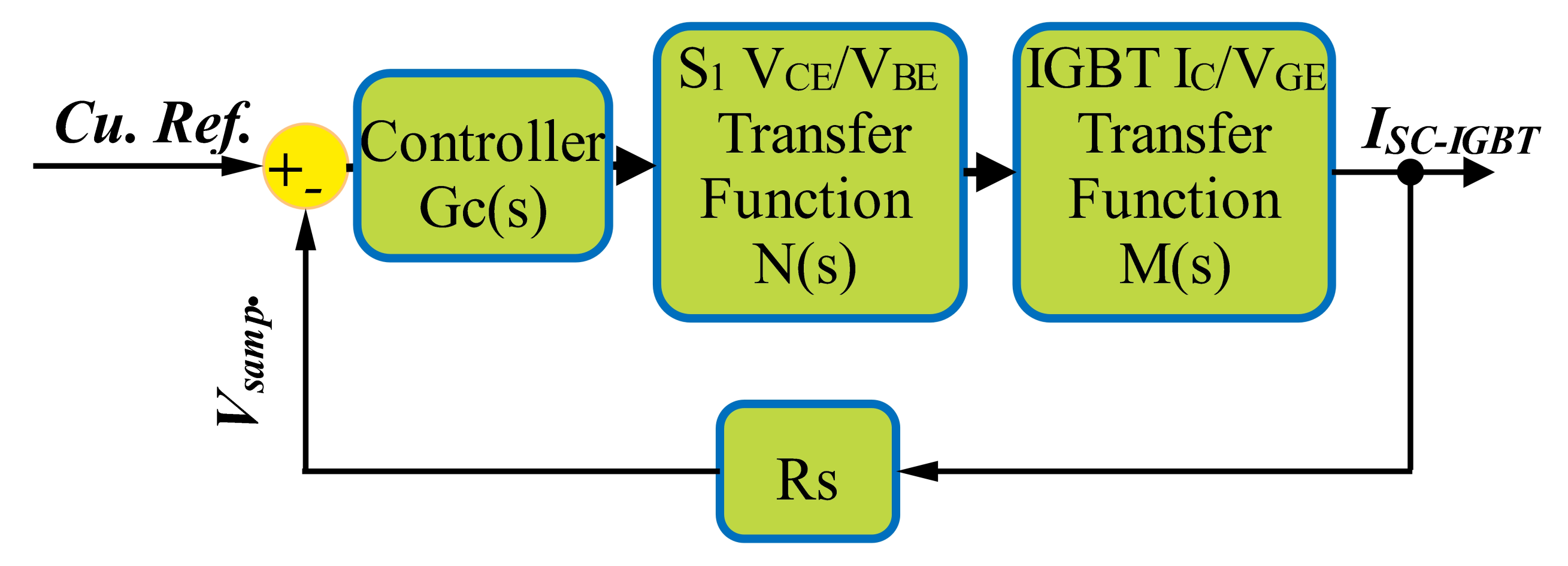
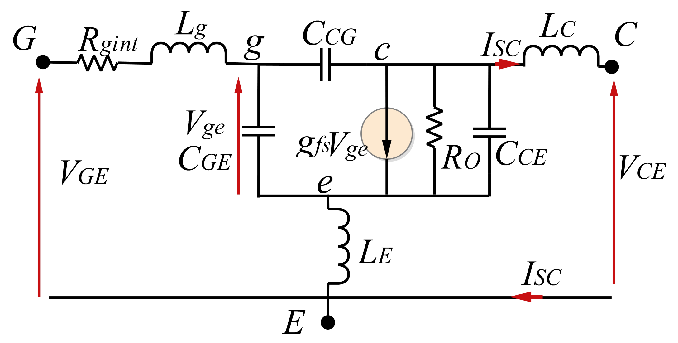
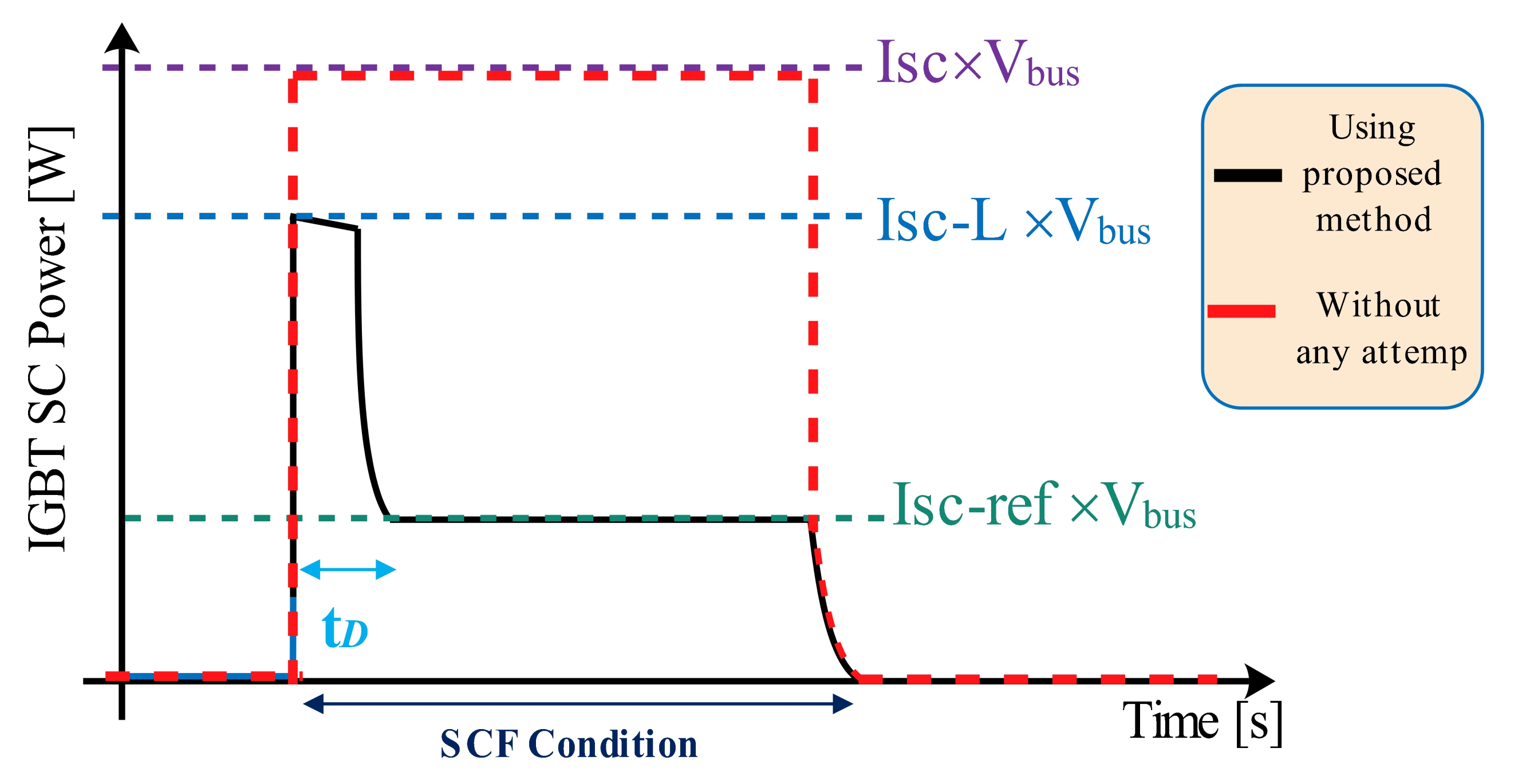
Using the SCF current limitation, this paper proposes a novel strategy for avoiding the failure modes under SCF conditions. When the SCF conditions occur, the IGBT peak current is restricted by a small value resistance. The SCF current amplitude is then controlled to a value much less than the maximum value reported in the IGBT datasheet. If the SCF is maintained for a longer period than is allowed, the IGBT is smoothly turned off. Our approach has the following advantages:
The junction temperature rise is much less than the case without current limiting.
The converter operation is not interrupted due to the temporary faults.
The IGBT failure modes in SCF relevant to the peak current can be more easily handled.
The first advantage is useful for the IGBTs with a small die where their junction temperature may considerably increase in SCF condition, and the failure in the turn-off state can be avoided by the proposed approach. The second advantage is applicable for mission-critical applications where the converter must be available seamlessly without any downtime for handling temporary faults. The third advantage can be used for all classes of IGBTs with different die structures and power ratings. The failure modes related to the IGBT SCF current, such as gate-oscillation, NDR, MOSFET mode, and self-turn off, can be easily managed. Our focus here is the temperature rise during the SCF, and the improvement in other failure modes is not the interest of this paper.
The rest of the paper is organized as follows: the proposed method is introduced in
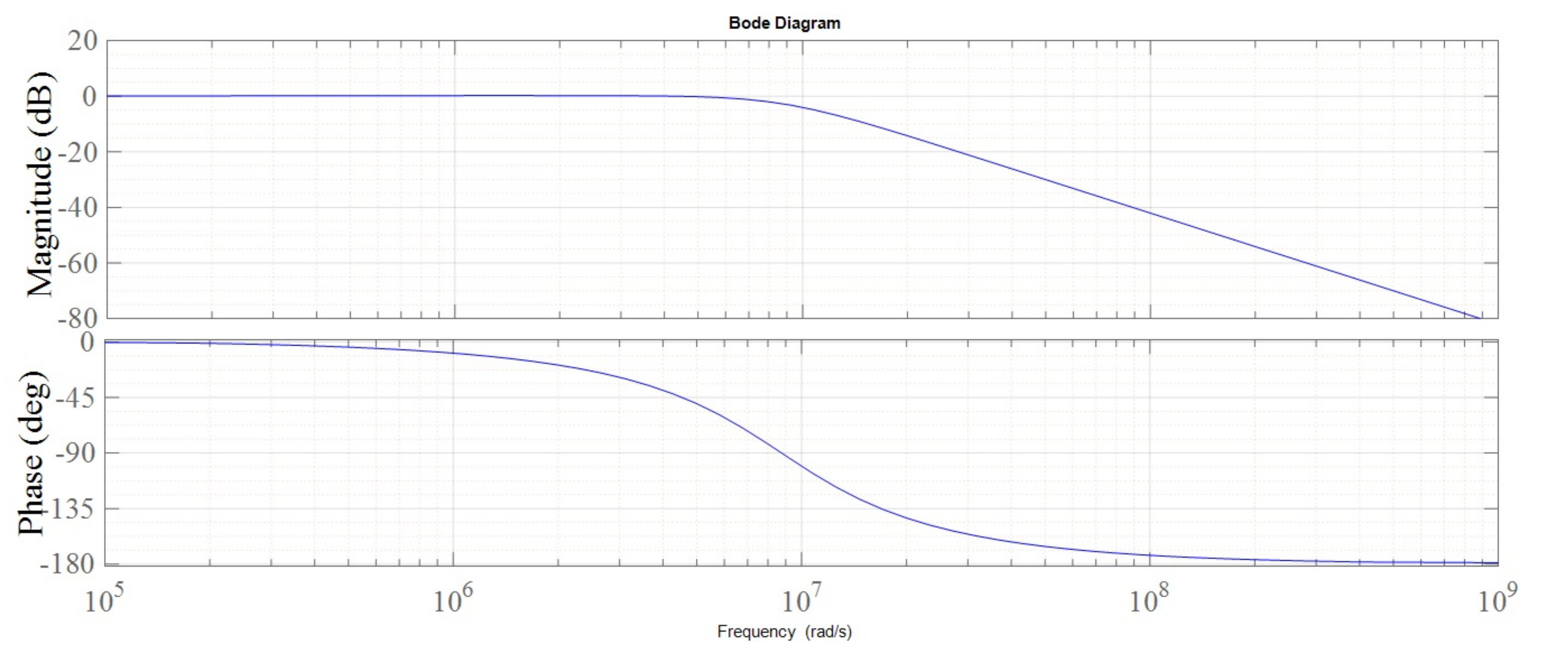
Section 2 where the operating principle, stability analysis, and improvements are described. The PSPICE simulations, finite element analysis are provided in
Section 3, and finally,
Section 4 provides the experimental results to validate the performance of the proposed method.
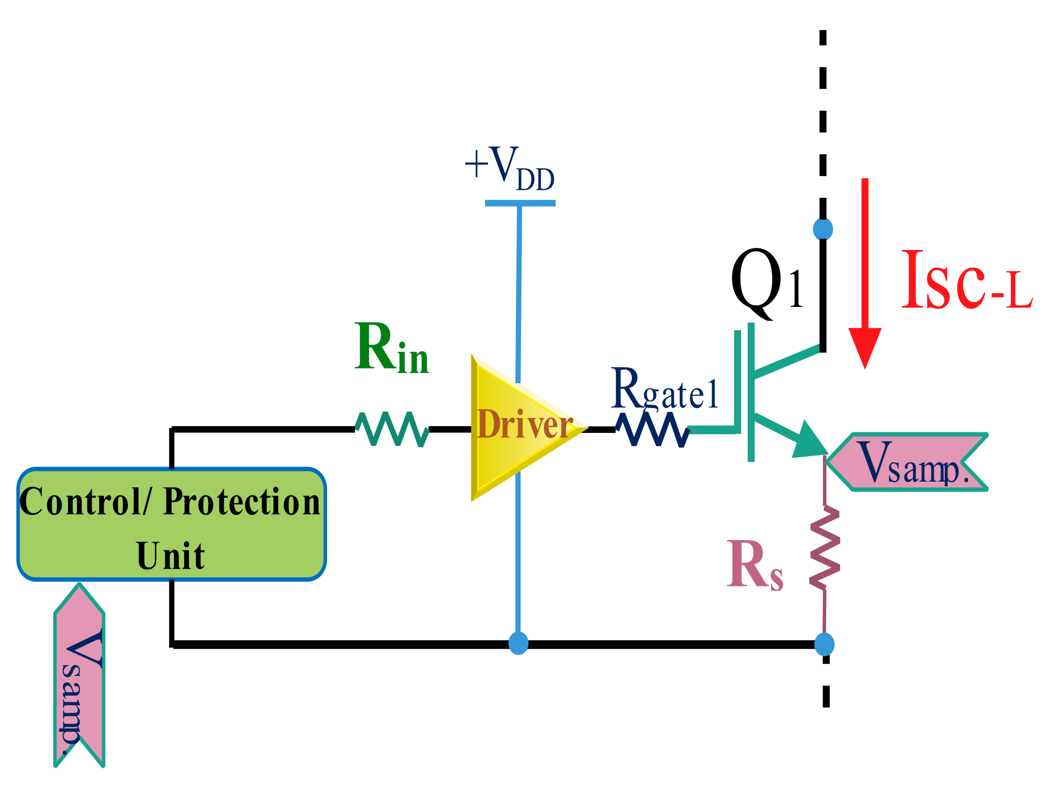
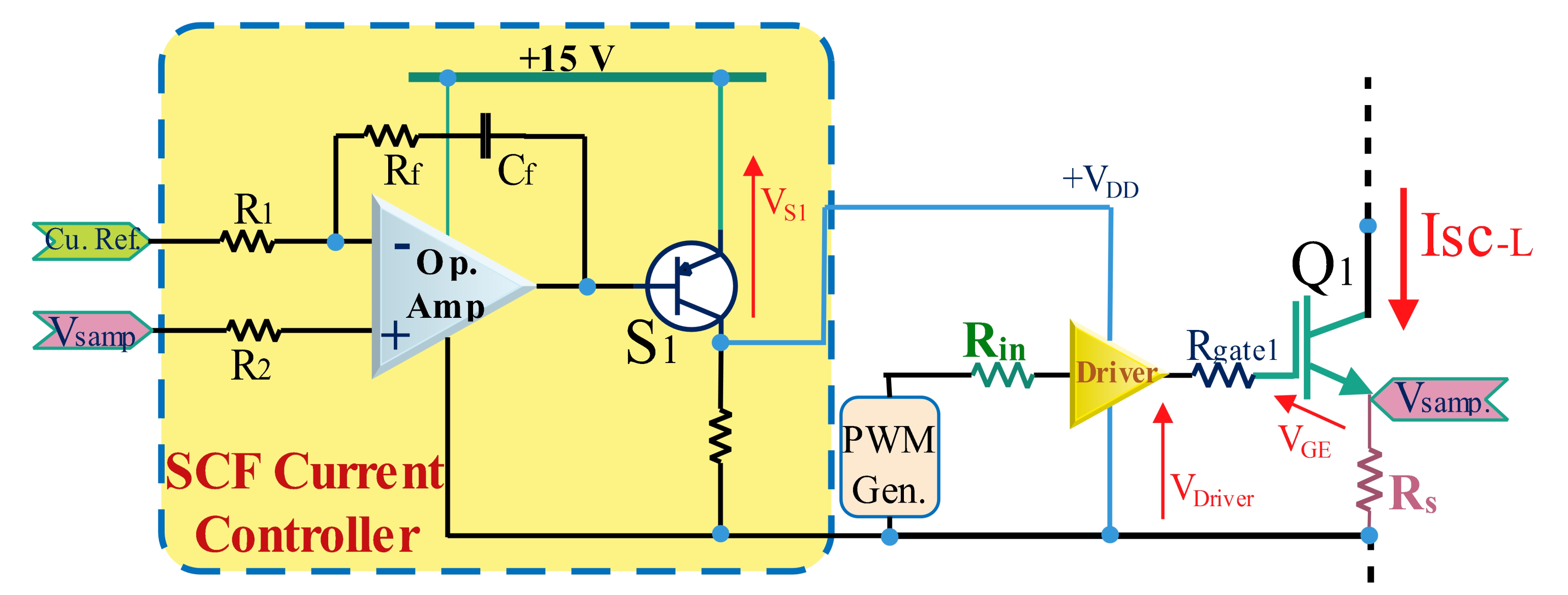
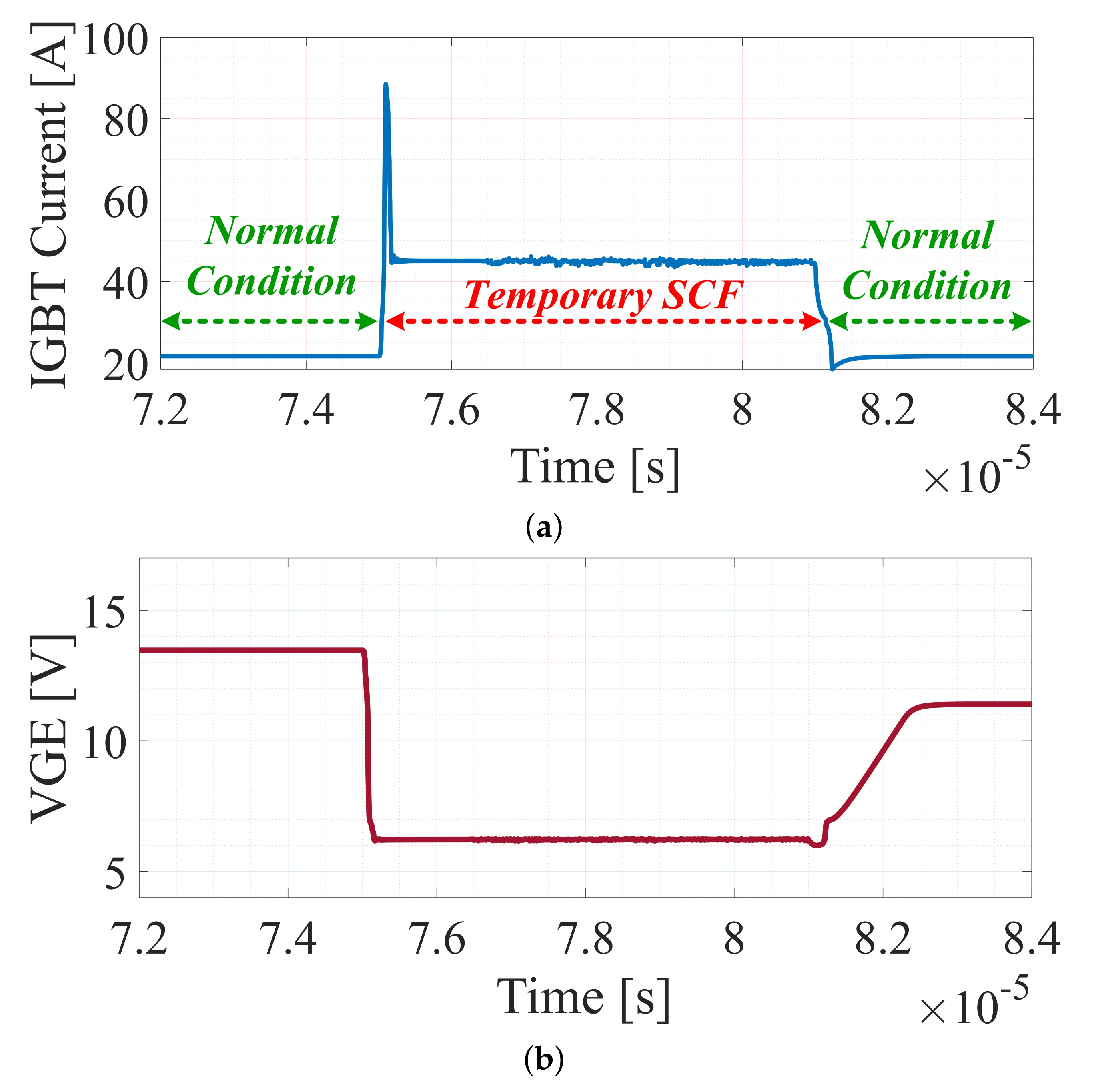
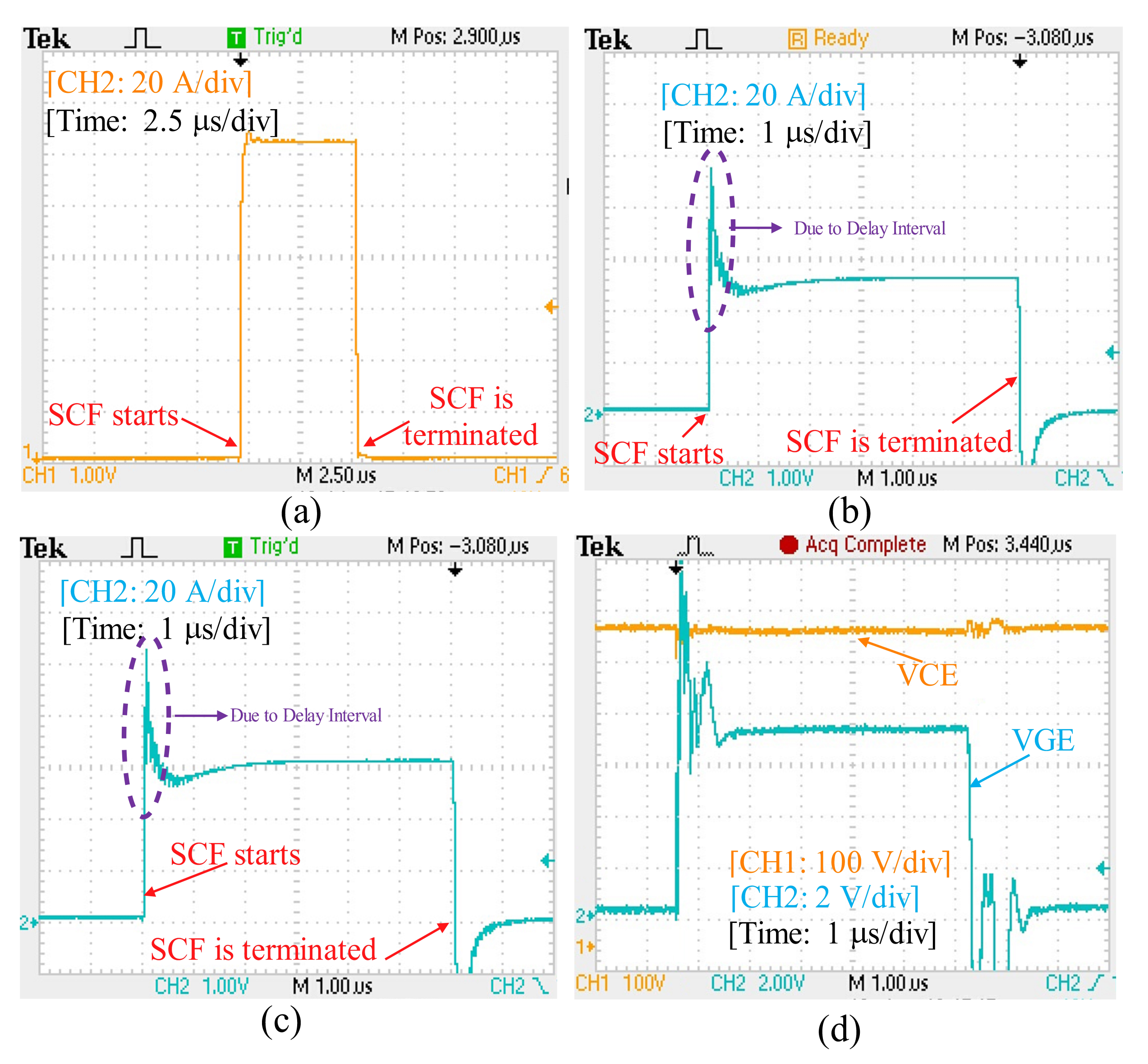
4. Experimental Results
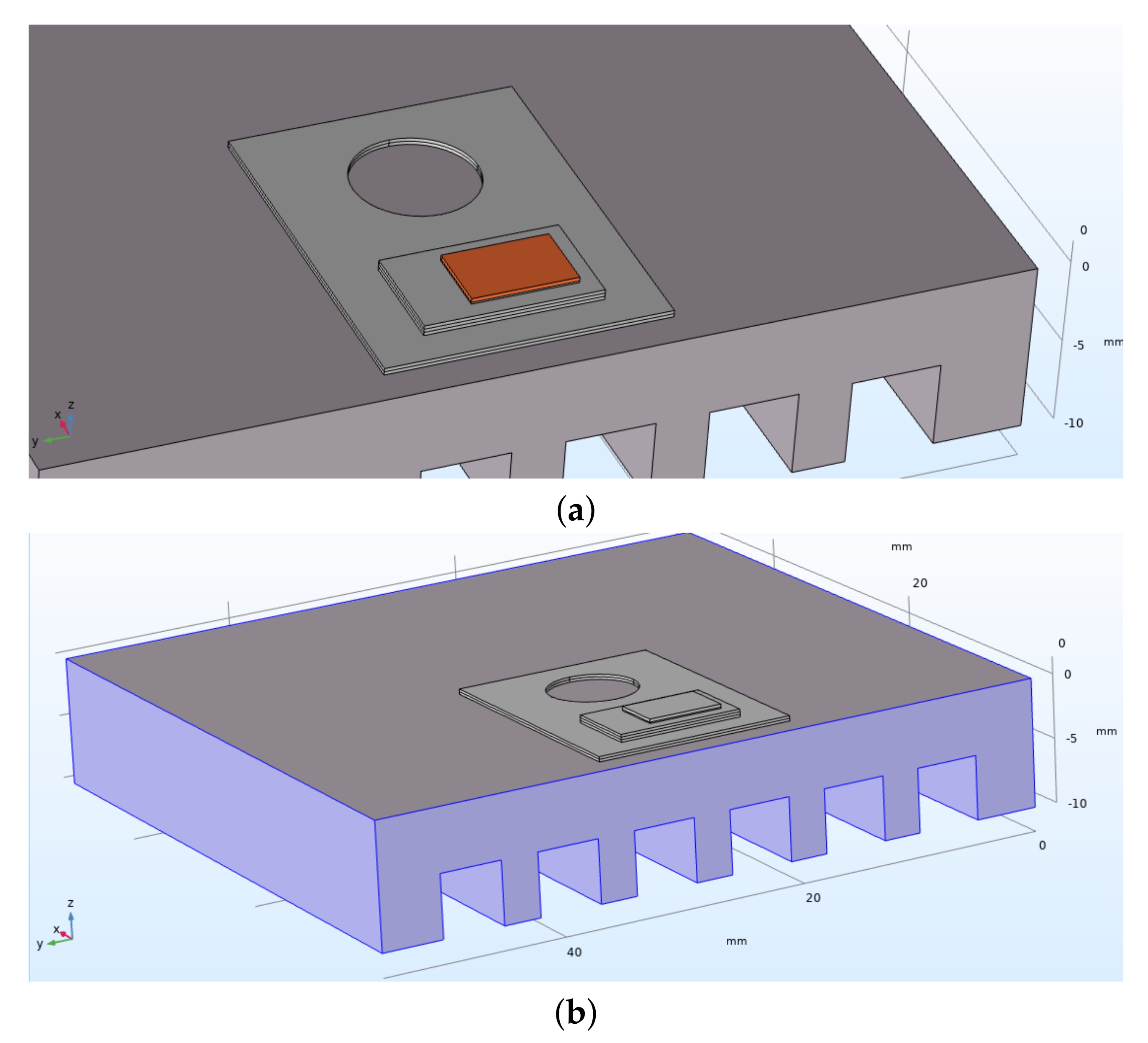
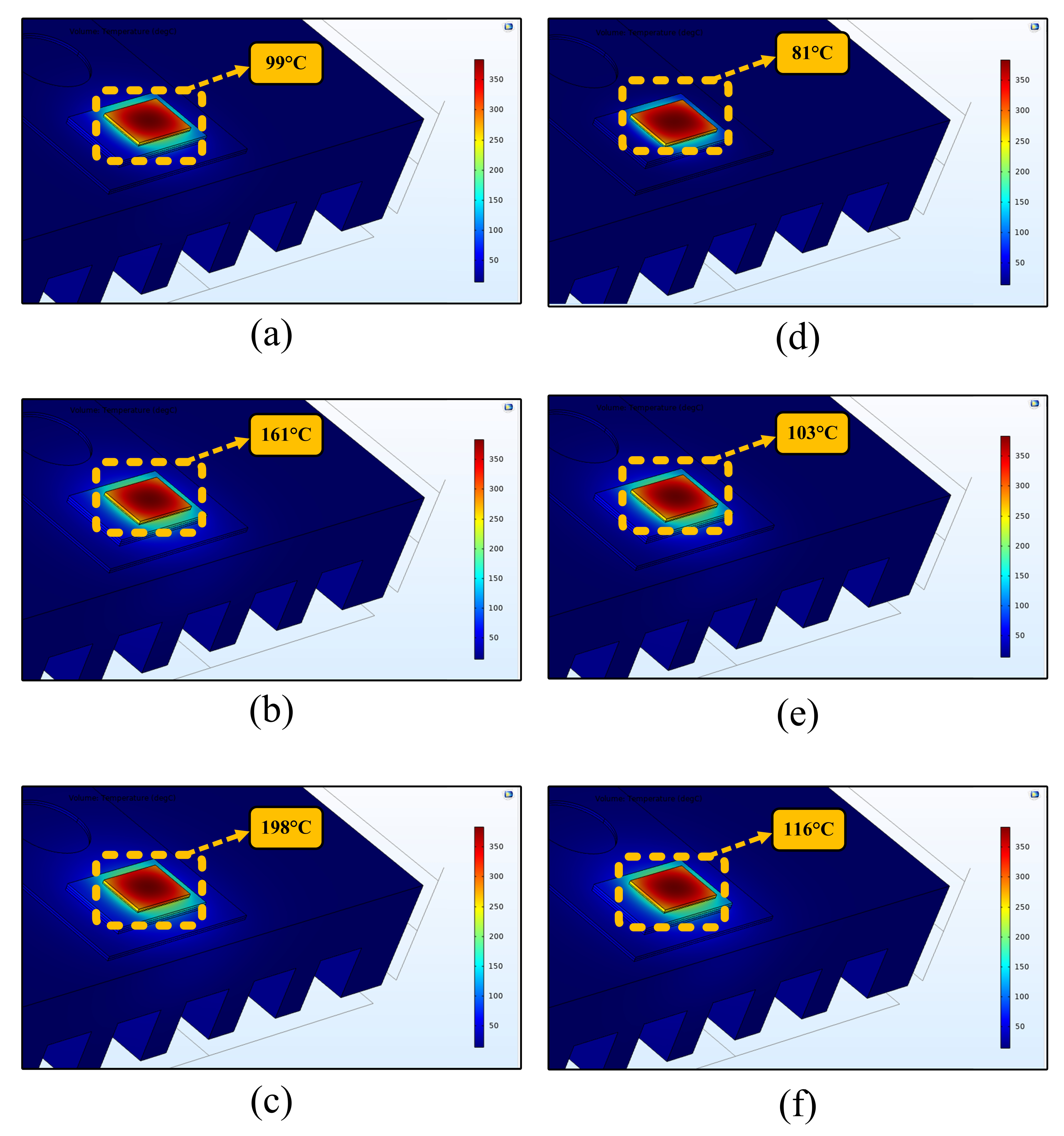
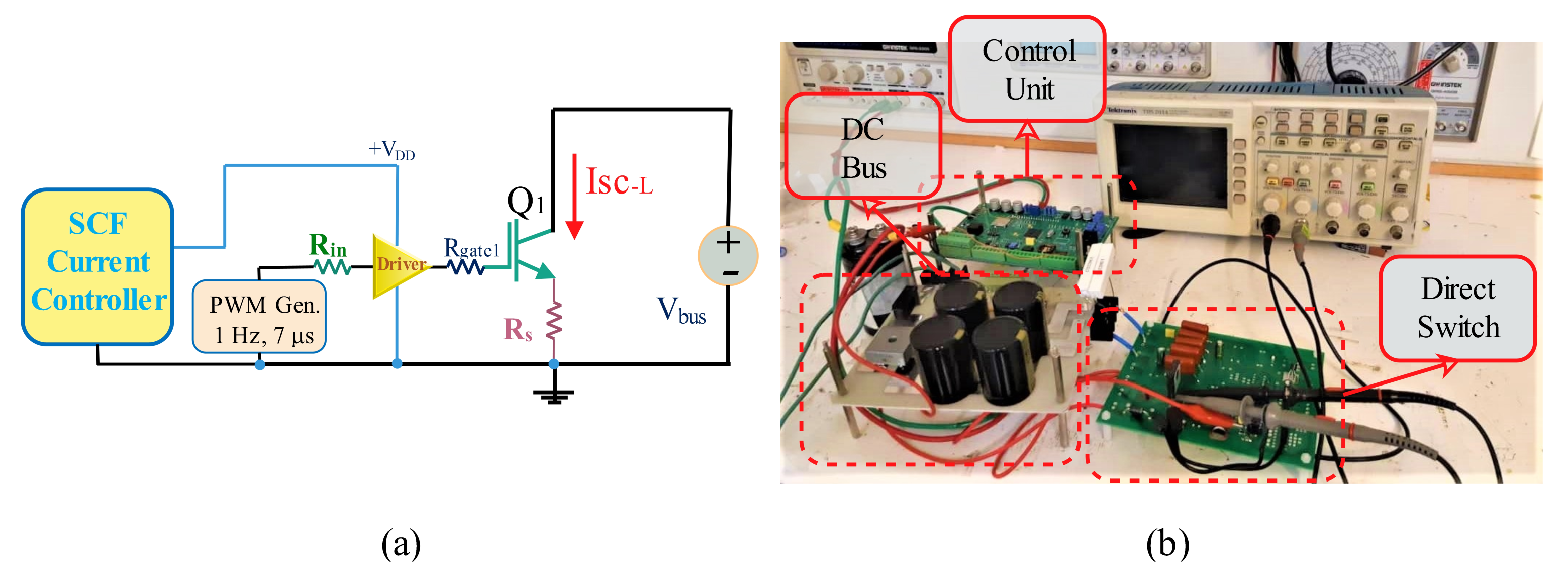
An experimental prototype is implemented to examine the proposed method. The considered case for the experimental evaluation has the same specifications as the simulation analysis (see
Table 3). In the tests, the IGBT is turned on in the SC condition. The block diagram of the experimental setup is provided in
Figure 16a. The overview of the experimental setup is presented in
Figure 16b. The SCF current is monitored by measuring the voltage drop across
. At the first step, the SCF current is observed without the proposed method. To this end, the driver voltage is fixed to 15 V, and the SCF current is observed using a current transformer. In this condition, the SCF current is presented in
Figure 17a. As seen, the SCF current amplitude equals 130 A without no attempt for limiting the current. In the second step, the limiting resistor as well as the control unit are added to the structure. The SCF current, when the SCF reference equals 50 A, is presented in
Figure 17b, in which it can be observed that after the delay interval, the SCF current is properly controlled to a value equal 50 A. To validate the SCF current controller, SCF reference is slightly increased to 65 A (see
Figure 17c).
Looking at
Figure 17b,c, the SCF current can be controlled to values much less than the potential SCF current (130 A), which can limit the temperature rise in SCF conditions. Accordingly, the SCF current can be effectively limited to a value equal to twice the load nominal current by the proposed method.
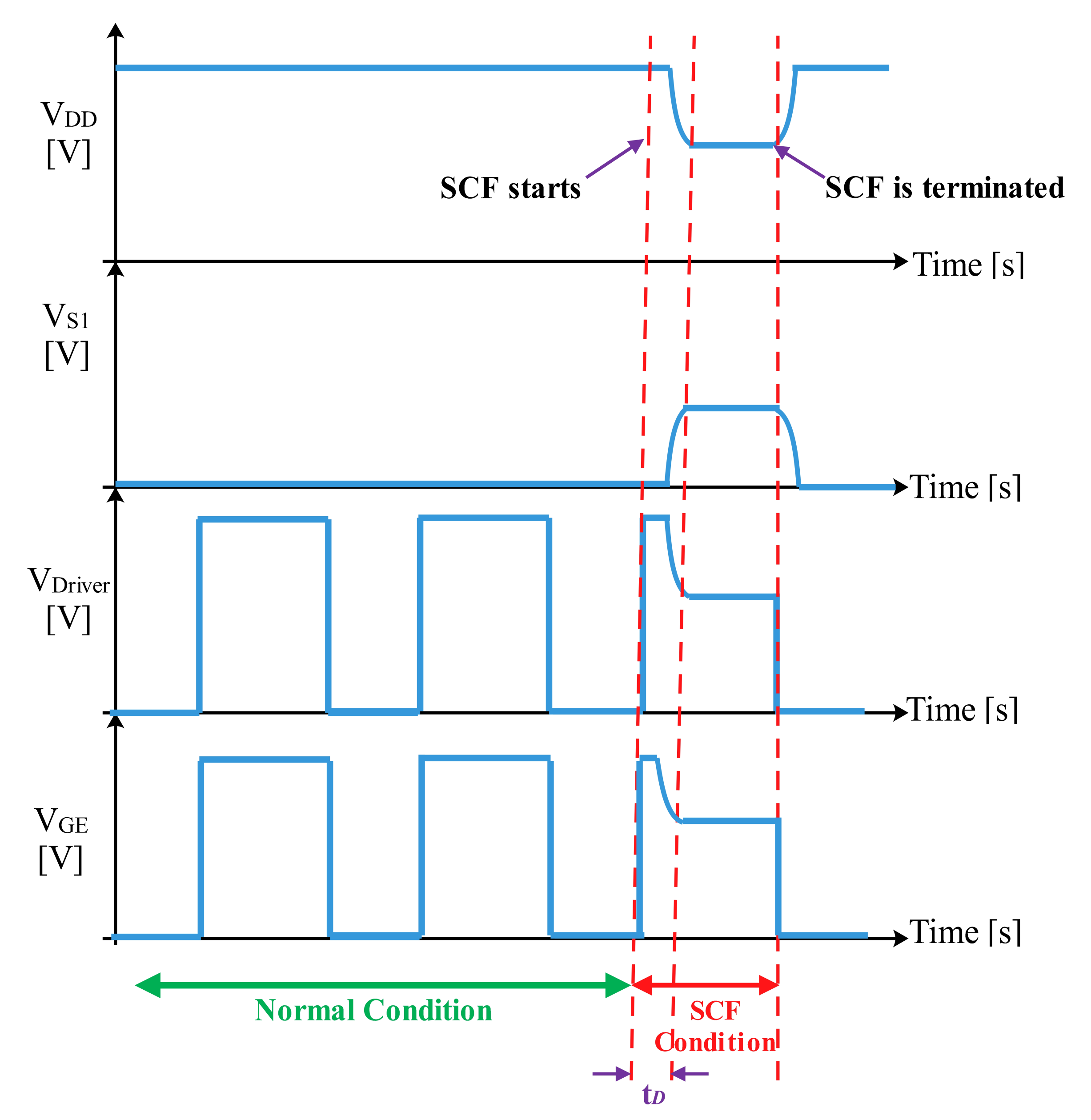
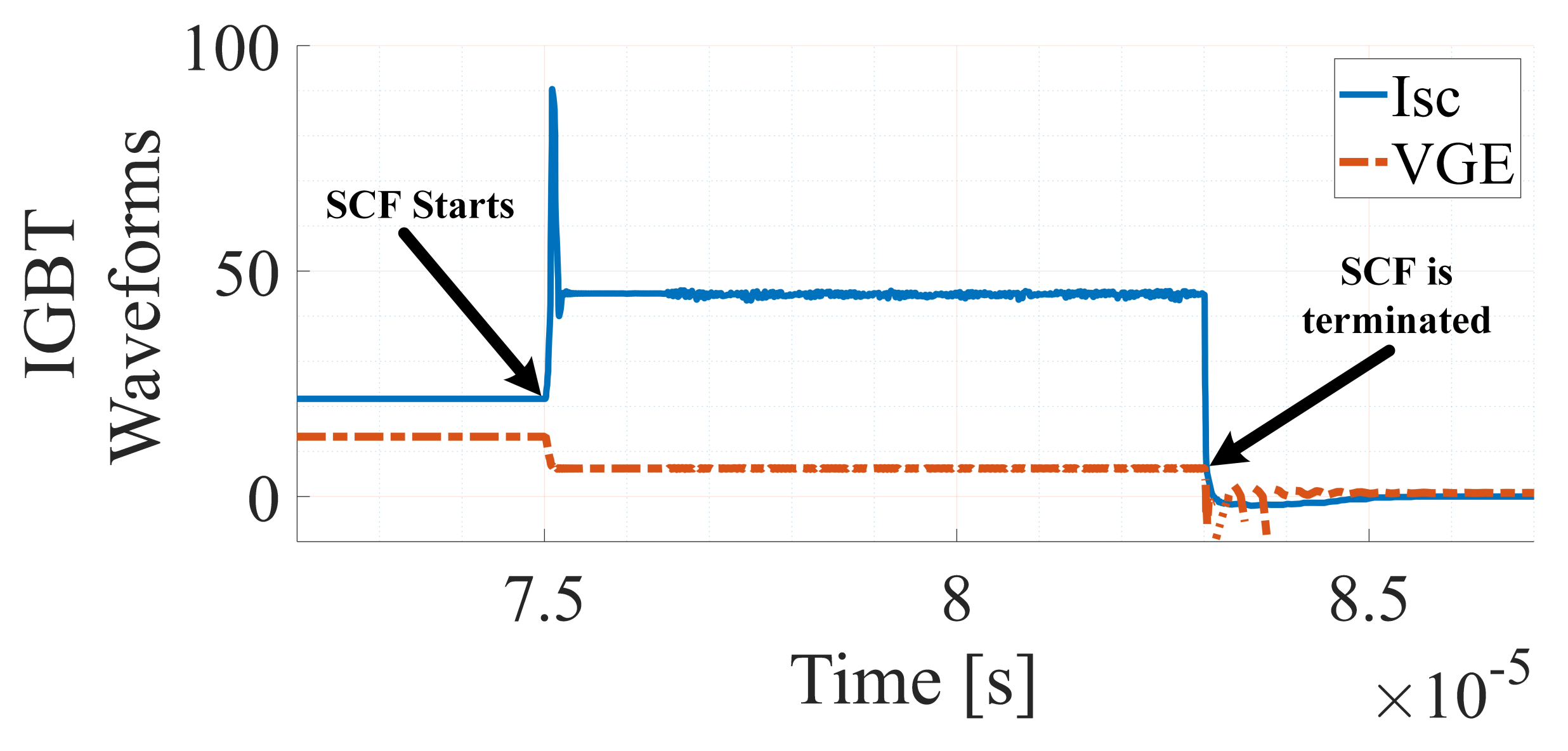
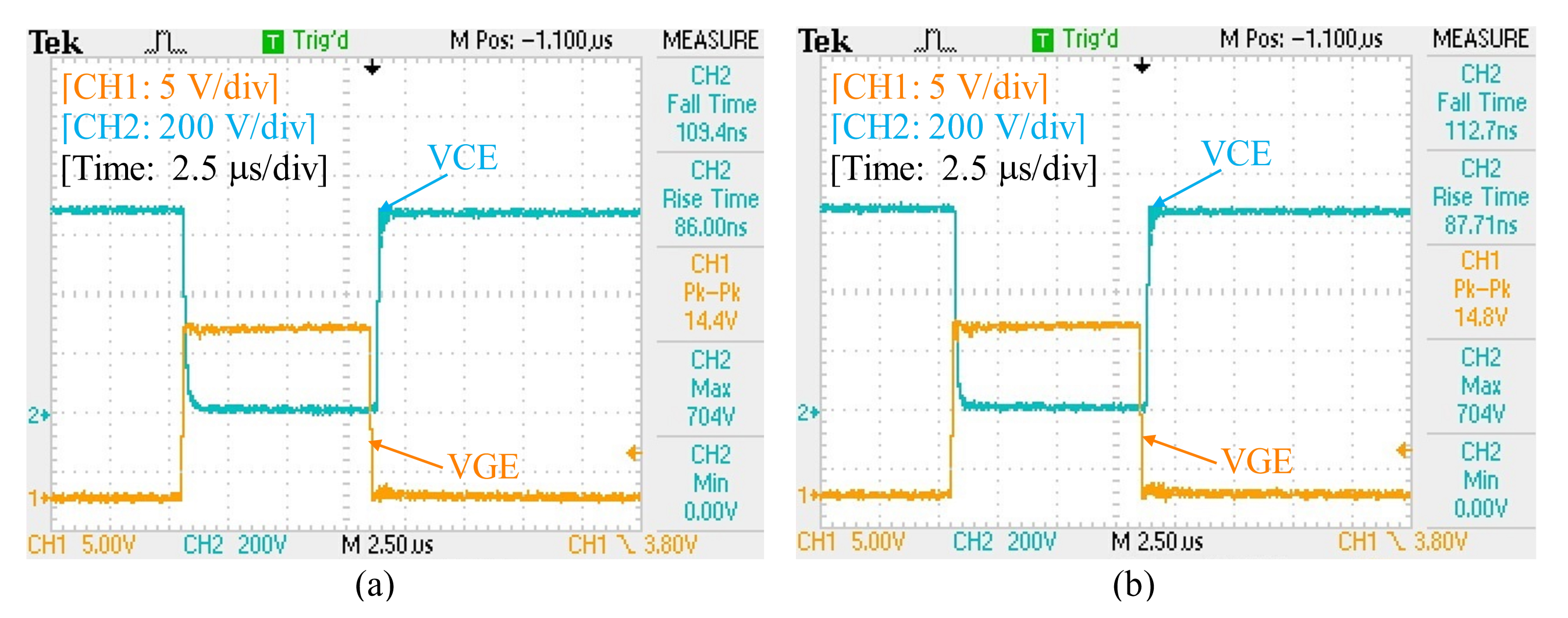
Figure 17d presents the gate-emitter and collector-emitter voltages of the IGBT under SCF condition, when the SCF is limited and controlled by the proposed method. Since the IGBT is turned on under the SCF condition, its collector-emitter voltage does not change from the turn-off state to the saturated region. The gate-emitter voltage, however, is decreased by the control unit to decrease the SCF current. As mentioned earlier, the proposed method does not slow down the device in the normal operation. Accordingly,
Figure 18 shows the waveforms of the device in the normal operation. Regarding
Figure 18, in the normal operation, the transient time intervals of the device with the proposed method (
Figure 18a) and without the proposed method (
Figure 18b) are approximately the same. Thus, it can be concluded that the proposed method does not affect the normal operation of the device. Considering
Figure 18, the only difference is related to the high-level voltage of the IGBT’s gate-emitter where using the proposed method, this value is 0.5 V less than that of the condition without the proposed method.
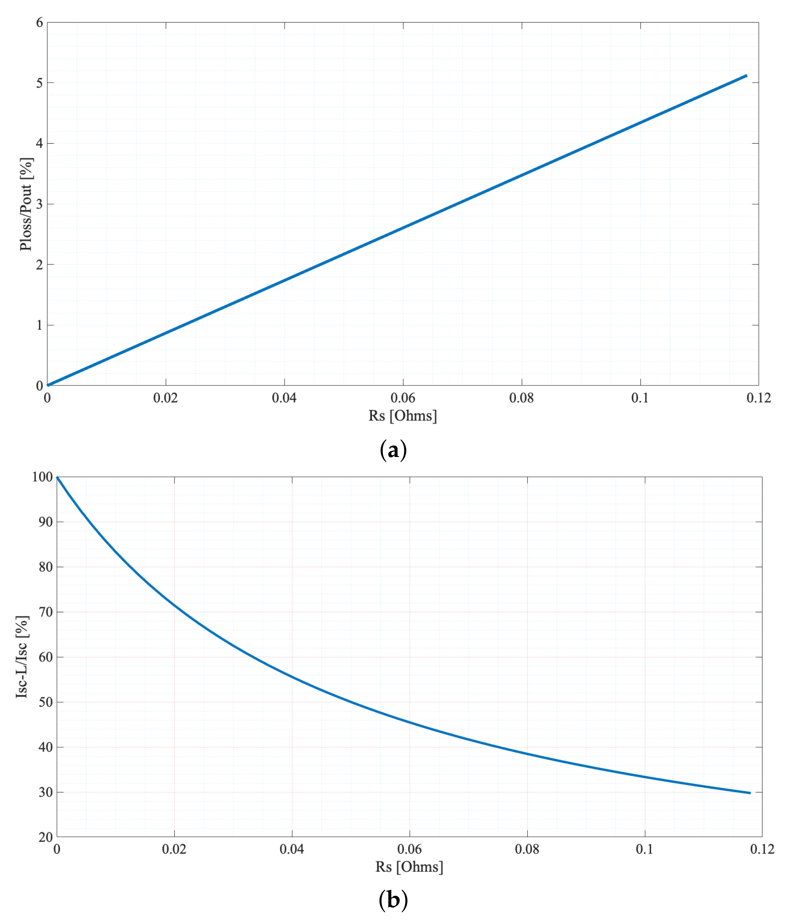
In the experimental prototype, the switching frequency is 10 kHz, duty cycle is 7%, equals 700 V, and load current has a 10 A peak value. Thus, the average power approximately equals 490 W. The value of is 0.05, and its dissipating power equals 0.35 W, which is far less than the converter output power.
Finally,
Table 6 compares the proposed method with extant methods. As can be seen, the proposed method has some advantages such as acceptable operation delayed operation, current controlling capability, and also does not have major effect on switch normal operation.


