Article

A Unified Controller for Multi-State Operation of the Bi-Directional Buck–Boost DC-DC Converter

by
Gabriel R. Broday
1,
Gilney Damm
2,
William Pasillas-Lépine
3 and
Luiz A. C. Lopes
1,*
1
Department of Electrical and Computer Engineering, Concordia University, Montreal, QC H3G 1M8, Canada
2
Department of Components and Systems (COSYS), University Gustave Eiffel, 93162 Paris, France
3
Laboratory of Signals and Systems (L2S), University of Paris-Saclay, 91190 Paris, France
*
Author to whom correspondence should be addressed.
Energies 2021, 14(23), 7921; https://doi.org/10.3390/en14237921
Submission received: 19 October 2021 / Revised: 12 November 2021 / Accepted: 18 November 2021 / Published: 25 November 2021
(This article belongs to the Special Issue DC-DC Converters Technologies, Applications and Optimization)

Abstract

:
DC grid interfaces for supercapacitors (SCs) are expected to operate with a wide range of input voltages with fast dynamics. The class-C DC-DC converter is commonly used in this application because of its simplicity. However, it does not work if the output voltage (V2) becomes smaller than the input voltage (V1). The non-isolated bi-directional Buck–Boost DC-DC converter does not have this limitation. Its two half-bridges provide a means for controlling the power flow operating in the conventional dual-state mode, as well as multi-state, tri, and quad modes. These can be used for mitigating issues such as the Right Half Plane (RHP) zero that has a negative impact on the dynamic response of the system. Multi-state operation typically requires multi-variable control, which is not easy to realize with conventional PI-type controllers. This paper proposes a unified controller for multi-state operation. It employs a carrier-based modulation scheme with three modulation signals that allows the converter to operate in all four possible states and eight different modes of operation. A mathematical model is developed for devising a multi-variable control scheme using feedback linearization. This allows the design of control loops with simple PI controllers that can be used for all multi-state modes under a wide range of operating conditions with the same performance. The proposed scheme is verified by means of simulations.

1. Introduction

Energy storage units such as supercapacitors (SCs) can provide fast varying currents for power balancing and voltage regulation of DC grids, provided they have a suitable interface: a power electronics converter and control scheme. A two-switch class C DC-DC converter is frequently used as the interface of SCs [1]. However, its dynamic response tends to be slowed down due to the presence of a Right Half Plane (RHP) zero in the transfer function of the output voltage (Vo) by the duty cycle (D) of the Boost mode. This can be addressed with a tri-state logic that eliminates the RHP zero at the expense of an addition switch and the use of a multivariable modulation scheme [2]. Another issue with the class C converter is that it loses its power flow control ability due to the conduction of the top anti-parallel diode when the DC grid voltage falls below the voltage of the storage device [3].
The 4-switch bi-directional Buck–Boost converter, with two half-bridges and an intermediate inductor as shown in Figure 1, can be used to overcome this issue. In fact, it was used in a DC bus fault protection scheme in [3,4]. Its ability to operate in the Buck, Boost, and Buck–Boost modes can be explored in several ways, including increased efficiency [5,6,7,8]. The tri-state logic has also been applied to the four-switch converter operating in the Buck–Boost mode for enhanced dynamic performance [9]. The main issue with the tri-state logic is that it concerns a multi-variable control problem with two variables, usually the ON and OFF duty cycles (Don and Doff) that need to be determined. The free-wheeling duty cycle (Dfw) is taken as the remainder of the switching period. In this case, if one wishes to control two state variables, the development of the small-signal model necessary for the design of linear controllers is complicated, leading to the appearance of cross-coupled transfer functions [10]. This can be addressed by keeping constant the duration of one of the states, typically Doff [9], or employing a dual-mode control scheme with parallel [11] or cascaded [12] control loops.
Linear PI-type controllers are often employed in power electronics interfaces [3,9,13]. These controllers are designed based on models linearized for a specific operating point and, as this operating point changes, their performance tends to degrade. In this scenario, for applications where a wide operating region is expected, such as the interface of SCs where the power flow direction changes and the SC voltage can also fall from rated to half-rated, non-linear control techniques have been employed [14,15,16]. However, due to their more complex nature, implementing such non-linear control approaches is still quite challenging. The use of dynamic feedback linearization employing well-known PI-type controllers has been seen as a good and effective alternative. This technique was used for the conventional dual-state control of uni-directional Buck, Boost, and Buck–Boost and bi-directional class-C converters in [17,18]. In [19], it was used for the four-switch bi-directional Buck–Boost converter operating either in the conventional dual-state Buck or Boost modes, with only one half-bridge switching at the time.
This paper presents a unified control scheme for the four-switch bi-directional Buck–Boost converter that allows it to operate in several multi-state (tri-state and quad-state) modes. In this way, the RHP zero that usually appears in the output voltage/current to duty cycle transfer functions related to the conventional dual-state Boost and Buck–Boost modes is eliminated, and the most efficient mode can be used for given operating conditions. A carrier-based Pulse-Width Modulation (PWM) scheme that allows the operation of the converter with dual-state, tri-state, and quad-state logic is presented. A model for the converter operating in multi-state with multi-variable control is developed. It is used to derive a unified control scheme based on feedback linearization for the control of the output voltage/current of the converter and the intermediate inductor current with simple PI controllers, independently. In the proposed scheme, one can have the converter operating in five different multi-state modes by converting control variables w1 and w2 from the control scheme, into three modulation signals u1, u2, and u3 according to given rules. Simulation results are used to show that the dynamic performance of the converter with the unified control schemed is essentially the same for the converter operating in any of the multi-state modes and for a wide range of input voltage and output current.
This paper is organized as follows. In Section 2, the multi-state carrier-based Pulse-Width Modulation (PWM) scheme and modes of operation of the DC-DC converter are introduced. Section 3 presents the mathematical model of the converter and the proposed control scheme with feedback linearization. Section 4 discusses an approach for obtaining the modulation signals for the PWM (u1, u2, and u3) from the control variables (w1 and w2) obtained in Section 3. A design example is presented in Section 5 and the performance of the proposed and conventional control schemes are verified in Section 6. The paper conclusions are stated in Section 7.

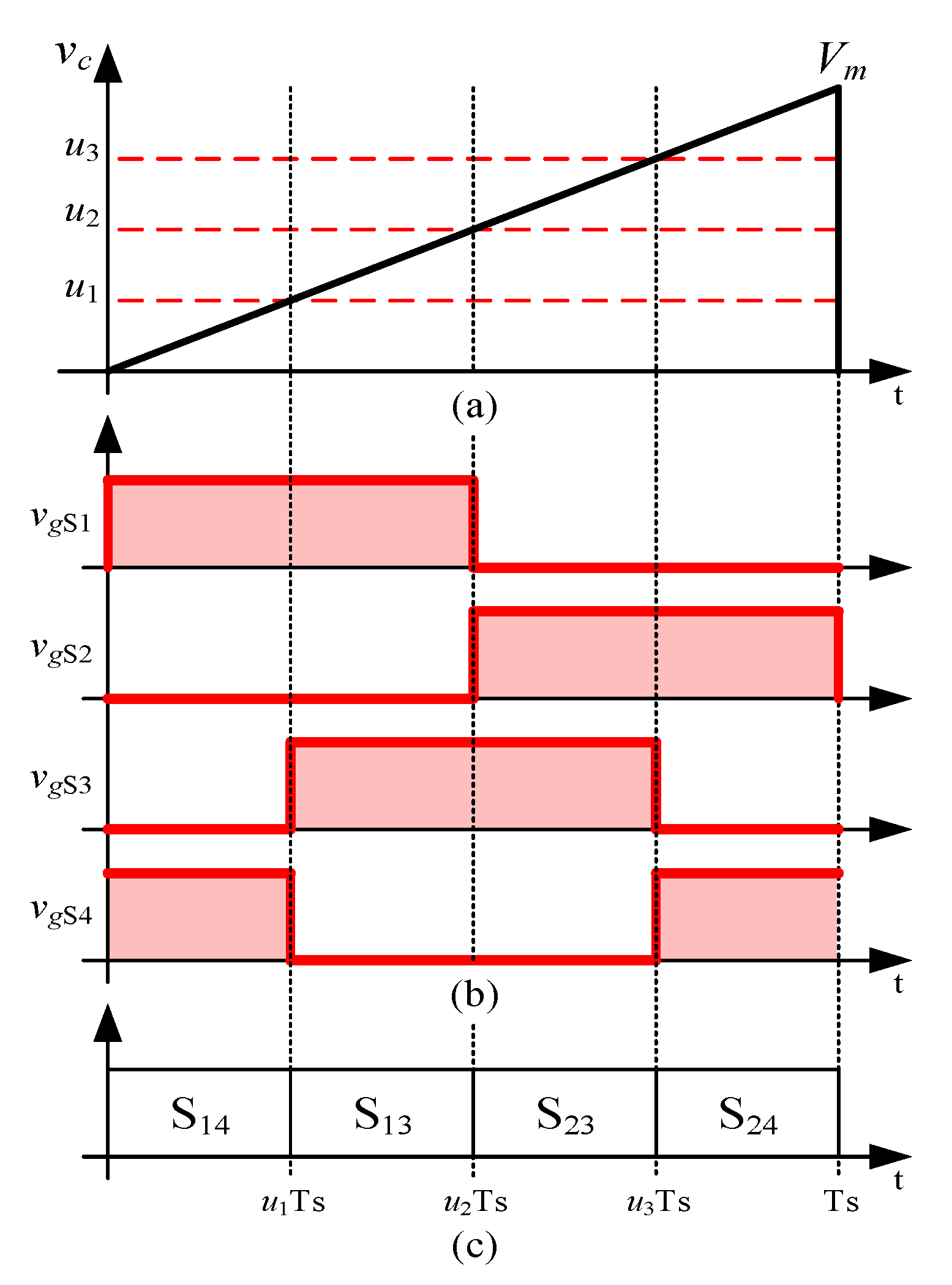
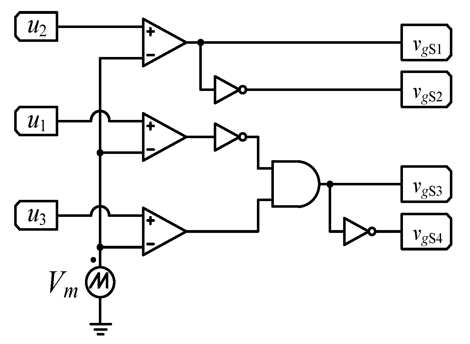
2. The Multi-State Carrier-Based Modulation Scheme

The proposed carrier-based Pulse-Width Modulation (PWM) scheme for the bi-directional Buck–Boost DC-DC converter is shown in Figure 2a. It presents three modulation signals, 0 ≤ u1u2u3Vm, where Vm is the peak value of the sawtooth carrier, which is usually assumed to be equal to 1. By comparing the modulation signals with the carrier using the circuit shown in Figure 3, one obtains the gating signals for switches S1, S2, S3, and S4, as shown in Figure 2b. All four possible states of operation for this converter (S14, S13, S23, and S24) are shown in Figure 2c. The subscript indicates the switches ON at a given time. From Figure 2, one can see that for Vm = 1:
u 2 = D 1
u 3 u 1 = D 3
where D1 is the duty cycle of S1 and D3 is the duty cycle of S3.
By setting additional constraints concerning the magnitudes of the modulation signals u1, u2, and u3, one can have the converter operating in eight different modes, as shown in Table 1. The modes in which the average voltage across the inductor (VL) cannot be made zero on a switching cycle basis are not useful/practical. It should be noted that for operation in Buck modes (1 and 4), it is mandatory that vC1 > vC2, while for the Boost modes (3 and 6) that vC1 < vC2. It has been shown that operation in the Buck and Boost modes, when possible, leads to lower power converter losses and stress on the switches than in the Buck–Boost mode [20].

3. Mathematical Model of the Converter

By employing KVL and KCL, one can obtain the following differential equations for the average values of the state variables of the converter:
d v C 1 d t = V 1 R 1 C 1 v C 1 R 1 C 1 i L C 1 ( u 2 )
d v C 2 d t = V 2 R 2 C 2 v C 2 R 2 C 2 + i L C 2 ( u 3 u 1 )
d i L d t = v C 1 L ( u 2 ) v C 2 L ( u 3 u 1 )
According to (3)–(5), the converter presents three state variables (vC1, iL, and vC2), and three control signals (u1, u2, and u3). Typically, one wishes to control either the output current of the converter (i2) or the output voltage of the converter (vC2), which require similar control actions. Frequently, this is achieved with an inner inductor current (iL) control loop and an outer current/voltage loop [3,9,13]. However, with the three modulation signals and the four possible states of operation (S14, S13, S23, and S24), one can have a certain value of vC2 or i2, with different values of iL, which is not the case for the conventional cascaded control scheme. This can be exploited for either reducing the losses in the converter, with a low value of iL, or having a faster dynamic response for the vC2, with a larger value of iL. Therefore, in this analysis, it is assumed that there will be a reference value for the average value of the output voltage (vC2*) and a reference value for the inductor current (iL*). These values are not independent, and a discussion on suitable values for iL* is presented in Section 3.4.
In order to control two of the state variables, one can employ two control variables. Therefore, by making the following change of variables:
w 1 = u 3 u 1
w 2 = u 2 ,  
one converts (3)–(5) into:
d v C 1 d t = V 1 R 1 C 1 v C 1 R 1 C 1 i L C 1 w 2
d v C 2 d t = V 2 R 2 C 2 v C 2 R 2 C 2 + i L C 2 w 1 = i 2 C 2 + i L C 2 w 1
d i L d t = v C 1 L w 2 v C 2 L w 1
Due to the cross-product between state and control variables, the equations presented above are non-linear. In such a case, one can design control loops for the average values of the output voltage (VC2) and inductor current (IL) based on the feedback linearization technique [17,18,19].

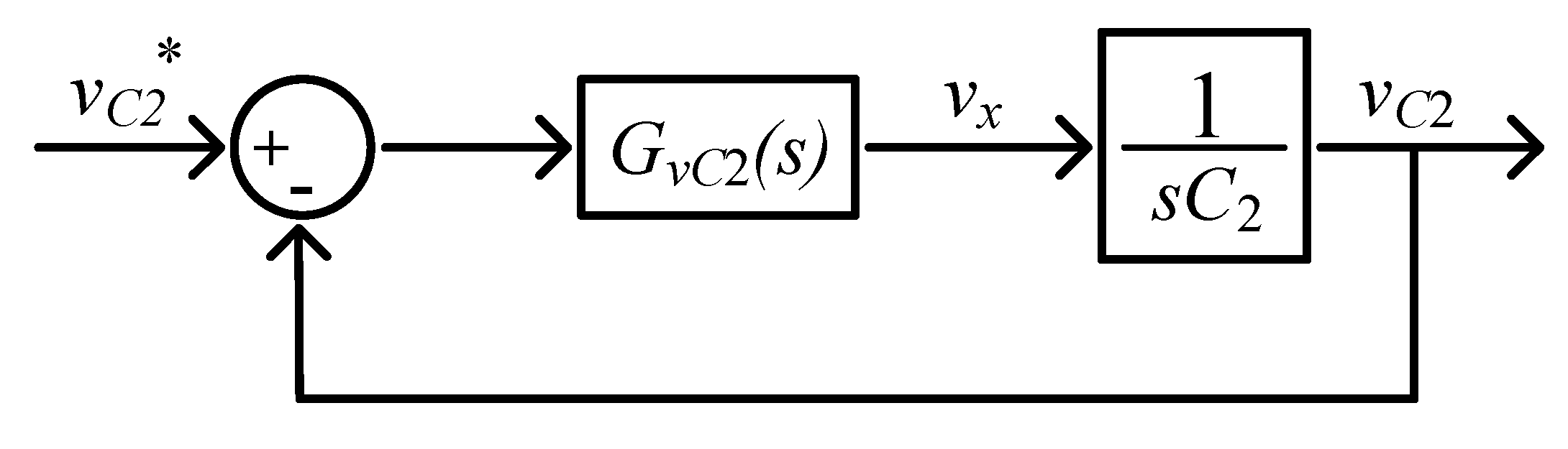
3.1. Output Voltage Control Loop with Feedback Linearization

For the design of the converter output voltage (vC2) controller, one can employ the feedback linearization technique. First, an auxiliary input variable (vx) related to vC2 and corresponding to iC2 is defined as:
d v C 2 d t = v x C 2
It provides a means for designing a linear PI-type controller (GvC2), as shown in Figure 4. Then, with vx being the voltage error (vC2* − vC2) processed by the PI controller, (11) becomes:
d v C 2 d t = 1 C 2 [ k p v   ( v C 2 * v C 2 ) + k i v ξ v ] = v P I v C 2
d ξ v d t = v C 2 * v C 2
It should be noted that vx is the output of the output voltage loop PI (vPIv), and it corresponds to iC2. In steady state, IC2 and VPIv should be zero. Finally, the value of the control variable w1 is obtained by substituting (9) in (12), leading to:
w 1 = 1 i L [ i 2 + k p v   ( v C 2 * v C 2 ) + k i v ξ v ] = 1 i L ( i 2 + v P I v )
There, one can clearly see the presence of the feedforward signals iL and i2, which should make the dynamic response of the performance of the vC2 control loop determined essentially by the PI-controller design specifications. Since 0 ≤ u1u2u3 ≤ 1, according to (6), one should have 0 ≤ w1 ≤ 1. While vC2 and V2 are expected to remain positive at all times, i2 and iL become negative as the direction of the power flow reverses, with VC2 < V2. When iL crosses zero, the value of w1 changes between ∞ and −∞, requiring a limiter to keep it within the (0–1) expected range.
From (9), one can say that in steady state, I2 = w1 IL with 0 ≤ w1 ≤ 1. iL and i2 should have the same sign, with the magnitude of iL being larger or equal to the magnitude of i2. In general, when one applies a positive step in vC2*, the positive error will make vPIv change from “0” to positive. If i2 and iL are positive, w1 increases so as to increase vC2. Conversely, if i2 and iL are negative, w1 decreases due to the negative sign of iL, which should make vC2 increase, since iC2 = w1iLi2. Therefore, the control law described in (13) should work for both forward and reverse power flows.

3.2. Inductor Current Control Loop with Feedback Linearization

The same procedure can be followed for the inductor current control loop. In this case, a second auxiliary input variable (vy), related to iL and corresponding to vL, is defined as:
d i L d t = v y L
It provides a means for designing a linear PI-type controller (GciL), as shown in Figure 5. With vy being the voltage error (iL* − iL) processed by the PI controller, (15) becomes:
d i L d t = 1 L [ k p i   ( i L * i L ) + k i i ξ i ] = v P I i L
d ξ i d t = i L * i L
One can see from Figure 5 that vy is the output of the inductor current PI controller, vPIi, and it corresponds to vL. In steady state, both VL and VPIi should be zero. The value of the control variable w2 is obtained by substituting (10) in (16), leading to:
w 2 = 1 v C 1 [ v C 2 w 1 + k p i   ( i L * i L ) + k i i ξ i ] = 1 v C 1 ( v C 2 w 1 + v P I i )
In the expression above, one sees the feedforward of signals vC1, vC2, and w1. Neither vC1 nor vC2 should present any challenges to the computation of w2, since they should be positive and not much different from V1 and V2. By feedforwarding w1, the dynamic response of the system should be determined by the current PI controller. Since 0 ≤ u2 ≤ 1 in the PWM scheme and according to (7), 0 ≤ w2 ≤ 1. Concerning the values of w1 and w2 in steady state, one can see from (10) that w2 > w1 if vC2 > vC1.

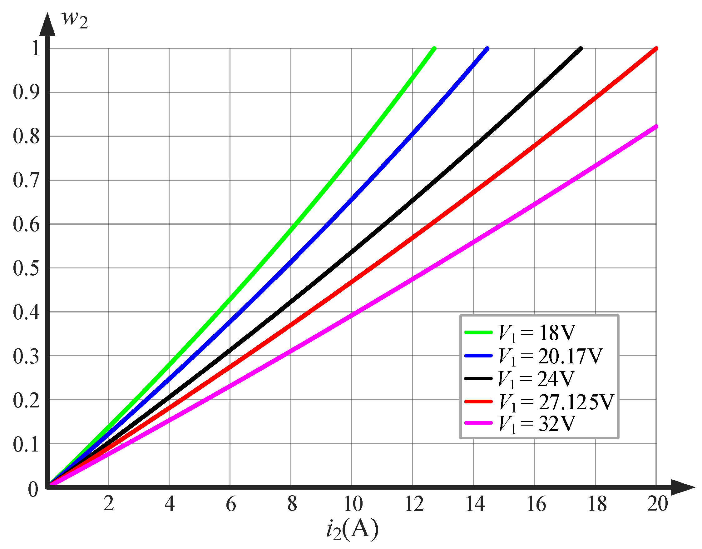
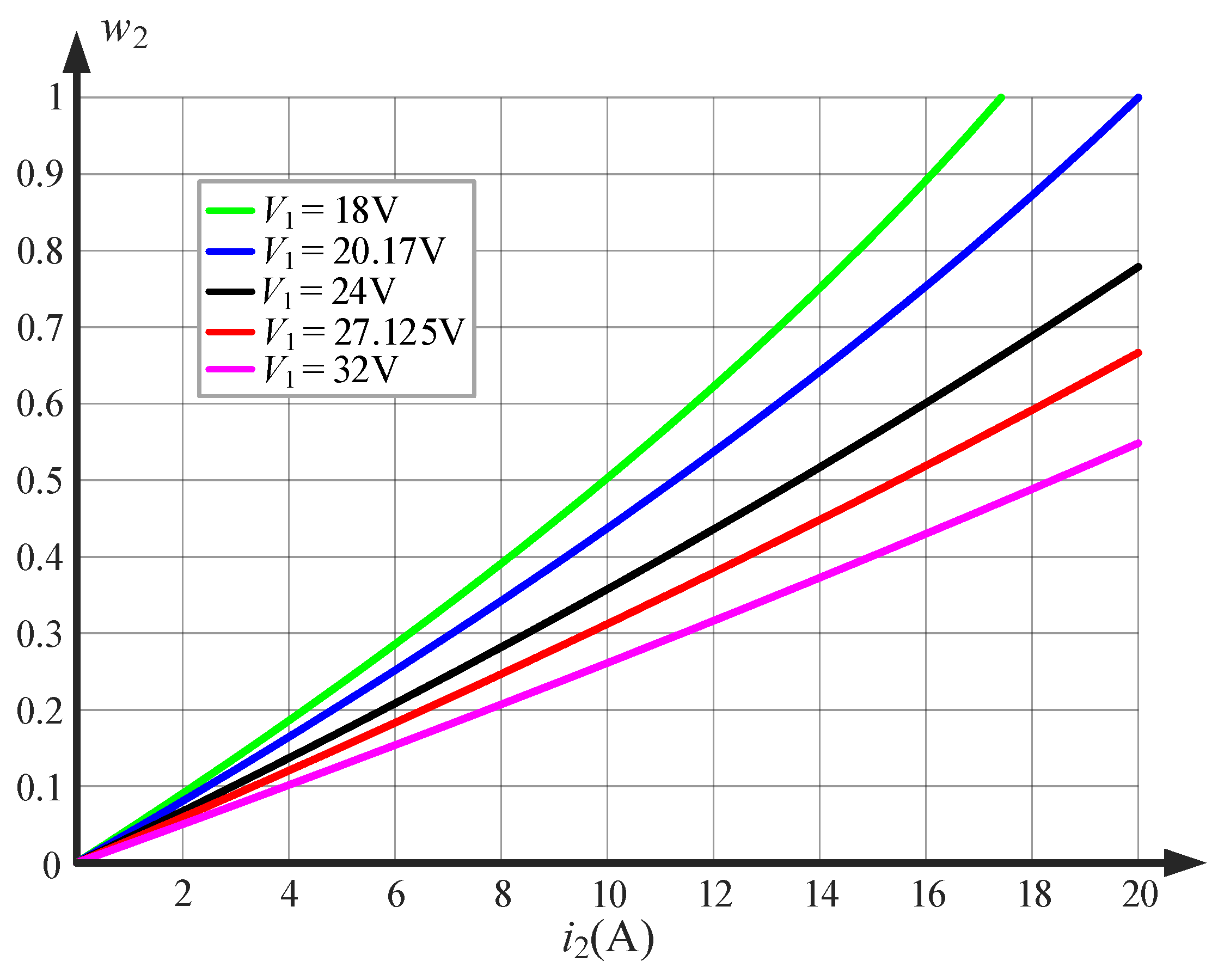
3.3. Impact of the Output Current and Input Voltage on the Choice of the Reference Inductor Current

As discussed in previous sections, variable w1 will be used for controlling vC2 and variable w2 will be used for controlling iL. Both control variables should be limited between 0 and 1. This will impose constraints on the possible values of V1, V2, and iL which are important to know. An equation describing this relationship can be derived from the equivalent circuit shown in Figure 6. It considers the reflection of the voltages V1 and V2 and resistances R1 and R2 to the intermediate (inductor) segment of the converter, using the principle of DC-transformer and the duty cycles of the S1–S2 and S3–S4 converter legs [21]. Based on (1), (2), (6), and (7) the duty cycles of the two legs, which correspond to the turns ratios of the DC transformers, can be computed as:
D 1 = w 2       and       D 3 = w 1
In general, by controlling vC2, one should be able to control i2, which is related to the inductor current by:
i 2 = w 1 i L
Therefore, for a given desired output current (i2) and a given value of inductor current (iL), a suitable value for w1 can be determined. Next, one can estimate a candidate value of w2 for given values of V1, V2, and iL for a specific value of i2 (≤ iL) and respective value of w1. For the operating conditions to be feasible, 0 ≤ w2 ≤ 1.
By using KVL in Figure 6, the following second-order equation can be used for calculating w2:
i L R 1 w 2 2 V 1 w 2 + i L R 2 w 1 2 + V 2 w 1 = 0
In order to have 0 ≤ w2 ≤ 1, with given values of V2, iL, R1, and R2 as w1 varies between 0 and a maximum value (w1max), there is a minimum value of V1 (V1min), calculated by
V 1 m i n = i L ( R 1 + R 2 w 1 m a x 2 ) + V 2 w 1 m a x
Figure 7 shows the values of w2 as a function of i2 with a maximum output current (i2max) of 20 A, for V2 = 48 V, iL = 40 A (fixed), and R1 = R2 = 62.5 mΩ for various values of V1. For this particular case, using (22) with w1max = 0.5, one obtains V1min = 27.125 V. From Figure 7, one can see that for values of V1 < V1min, one cannot have 0 ≤ i2i2max with 0 ≤ w2 ≤ 1. Conversely, for V1 > V1min, one can have 0 ≤ i2i2max with 0 ≤ w2 ≤ 1.
Alternatively, one can use a larger iL, say 60 A, and a smaller w1max, say 0.33, for i2max = 20 A. In this case, one computes V1min = 20.17 V. Figure 8 shows the values of w2 as a function of i2 (w1iL, 0 ≤ w1 ≤ 0.33), for V2 = 48 V, iL = 60 A, and for various values of V1. As in the previous case, an i2max of 20 A can be obtained with 0 ≤ w2 ≤ 1, as long as V1V1min. In general, in order to decrease V1min, it suffices to increase iL. By using a lower w1max, one increments the Boost effect that allows the use of a lower input voltage.

3.4. Reference Value for the Inductor Current

In the analysis presented in the previous section, a constant reference inductor current (iL*) is considered. One issue is that for a low value of i2*, a low value of w1 is used. If one wishes to reduce vC2*and i2*, the value of w1 will decrease and possibly saturate, slowing down the dynamic response. If one wishes to reverse the power flow, both i2 and iL need to be reversed. The value of iL* should change from, say 60 to −60 A, which will take more time to realize than if the current variation was smaller.
Another option is to determine a value for iL* as a function of i2. One of the requirements of this converter is that since 0 ≤ w1 ≤ 1 and i2 = w1 iL, 0 ≤ |i2| ≤ |iL|. This can be based on a gain (ki2L), where iL* = ki2L i2, which is the inverse of the value of w1 in steady state. To keep w1 not too low, so that it can be decreased to regulate vC2 without saturating at the minimum value, one can select ki2L = 3, for w1 = 0.33. This matches with the conditions shown in Figure 8, where for i2max = 20 A, iL = 60 A, and one can operate with V1min = 24 V.

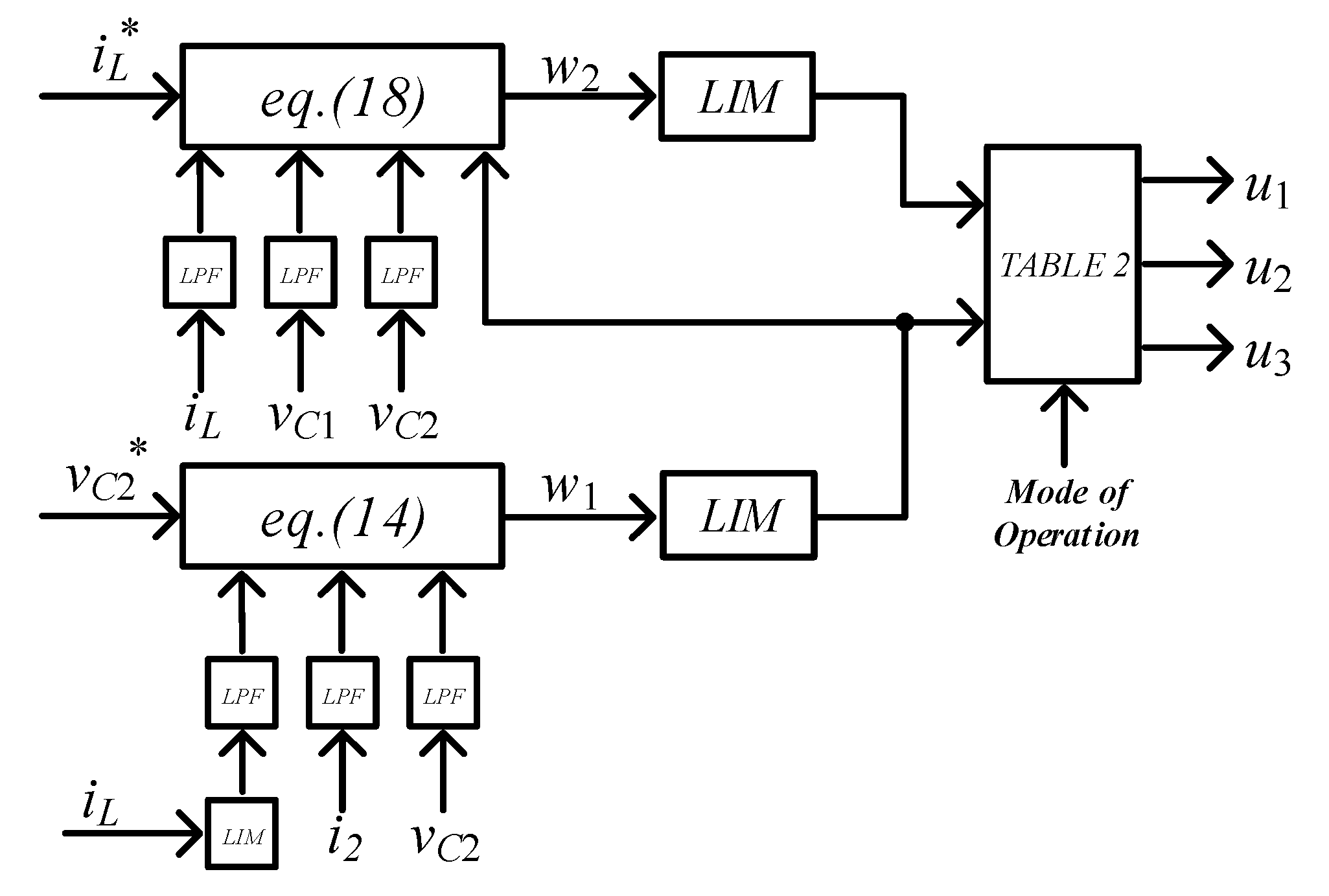
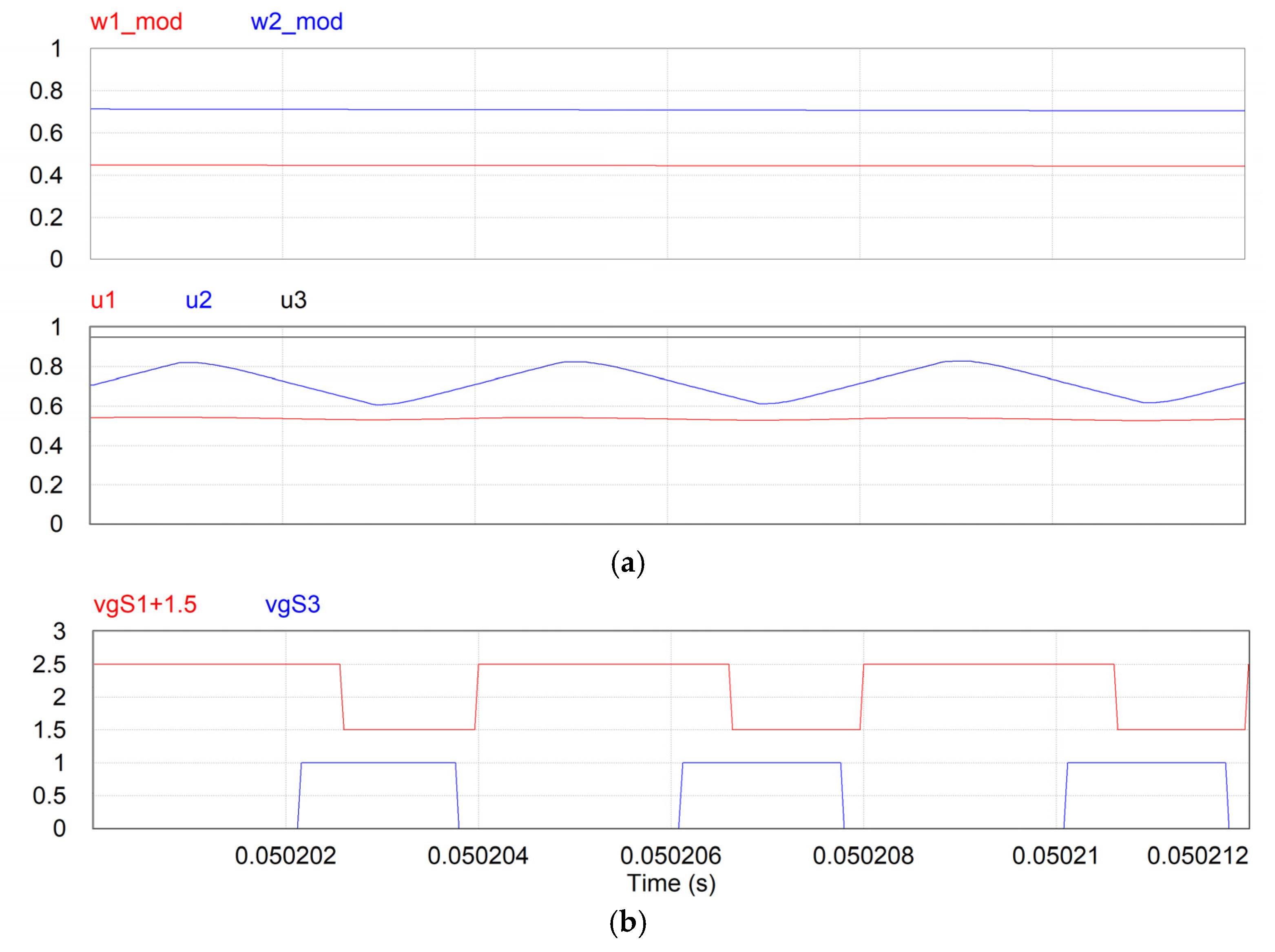
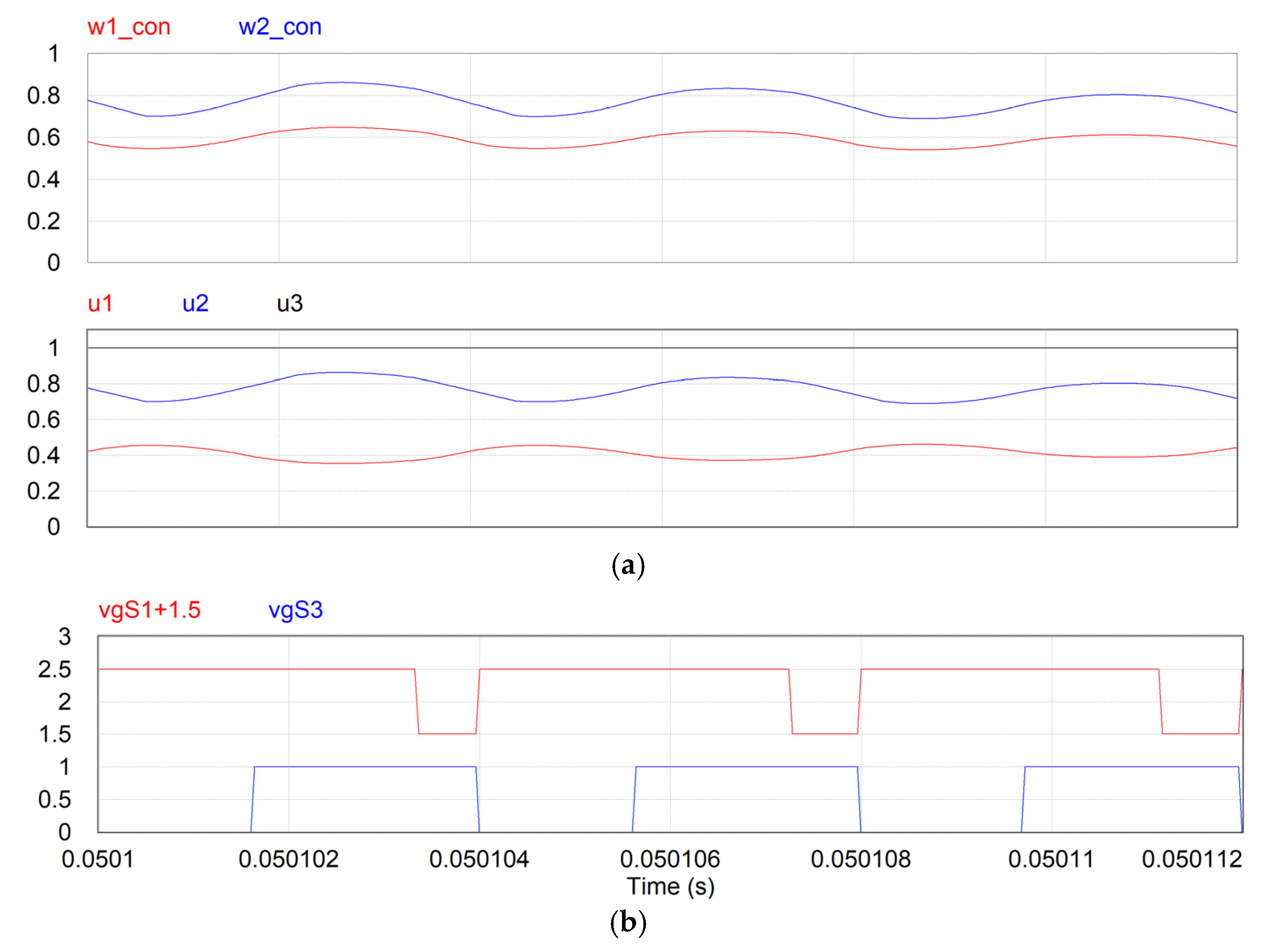
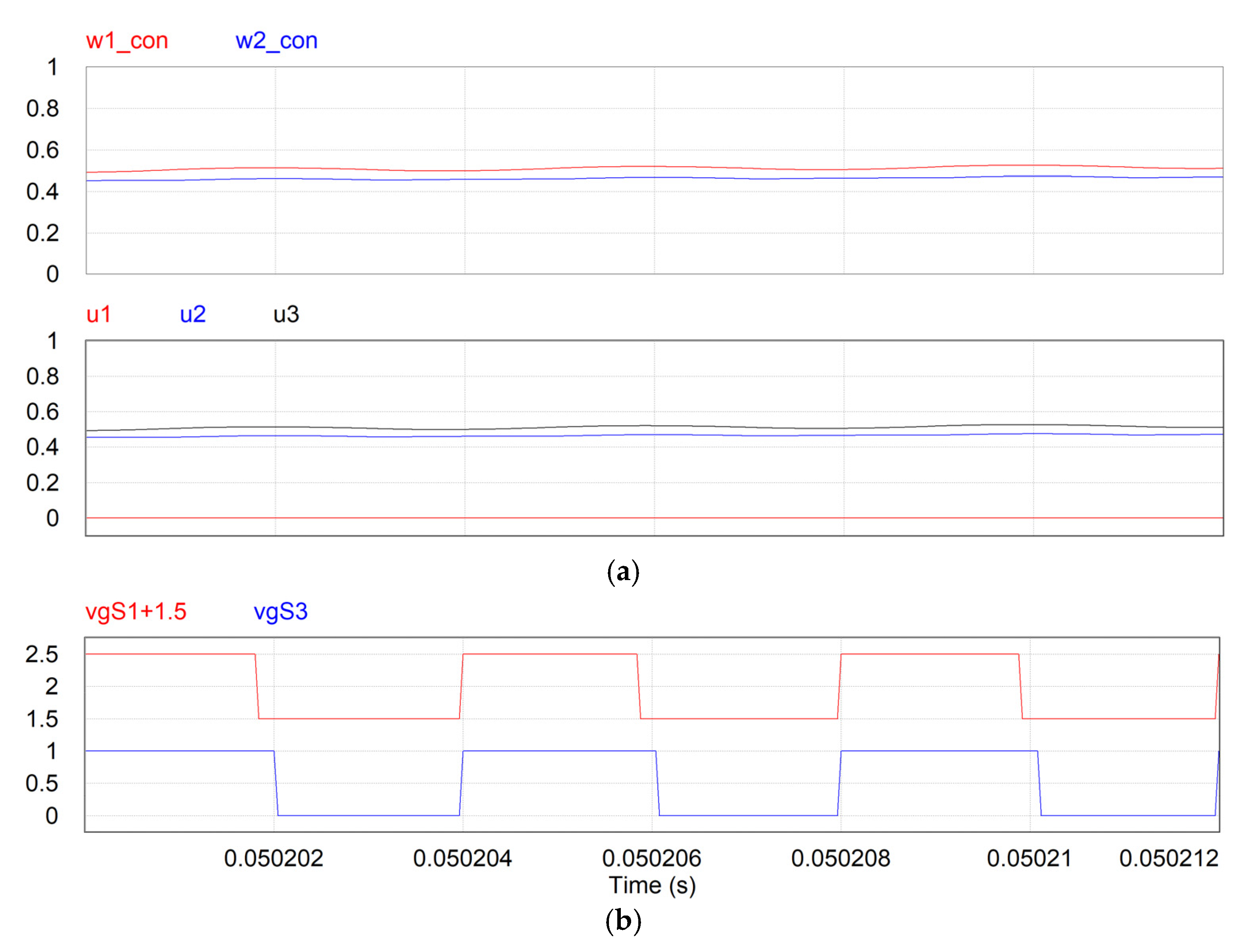
4. Obtaining u1, u2, and u3 from w1 and w2

The control scheme developed in Section 3 for vC2 and iL considered control variables w1 and w2. For the actual implementation of the proposed multi-state PWM scheme, one needs the modulation signals u1, u2, and u3 for generating the gating signals of the switches. As shown in Table 1, there are eight possible modes of operation for the non-isolated bi-directional Buck–Boost DC-DC converter. Only those that allow independent control of w1 and w2 can be used with the proposed control scheme. Based on the values they employ for u1, u2, and u3, one can say that only modes 4–8 comply with this condition. Another aspect to be considered is whether they are compatible with the input and output voltages in the circuit. For instance, mode 4 (tri-state Buck) can only be used when vC1 > vC2, while mode 6 (tri-state Boost) can only be used when vC1 < vC2. Conversely, modes 5, 7, and 8 (tri-state Buck–Boost and quad-state) can be used for all cases.
Table 2 shows how to obtain u1, u2, and u3 from w1 and w2 for the five multi-state modes. For mode 5 (tri-state Buck–Boost with no free-wheeling), since 0 ≤ u1u2, then 1 ≤ w1 + w2. For mode 6 (tri-state Boost with free-wheeling), w1w2. Finally, for mode 8 (quad-state), one can use a constant large value for c, say 0.95, while ensuring that w1w2c.

5. Design Example

The following parameters were selected for a case study that concerns the interface of a supercapacitor rated at 48 V to a DC grid also rated at 48 V. It is assumed that the voltage in the supercapacitor (V1) can vary between rated and half-rated (24 V ≤ V1 ≤ 48 V). Concerning the DC-grid voltage (V2), it is assumed that it can vary by +/− 5% around the rated value; thus, 45.6 V ≤ V2 ≤ 50.4 V. The other converter parameters are R1 = R2 = 62.5 mΩ, C1 = C2 = 76.8 μF, L = 38.8 μH, fsw = 250 kHz, −20 A ≤ i2 ≤ 20 A.

Controller Design

Based on (11) and (15), one only needs the value of C2 and L, respectively, to design the output voltage and inductor current controllers. Since in the actual switched converter, voltages and currents present switching harmonics, first-order Low-Pass Filters (LPFs) of 100 kHz are employed in both control loops. The bandwidth of the inductor current control loop (fx_iL) is selected as 50 kHz (20% of fsw) and its phase margin is selected as 60°. Since the output voltage of the converter (vC2) is regulated based on the switching of the inductor current, the bandwidth of the voltage control loop is selected as 10 kHz (20% of fx_iL) and its phase margin is selected as 60°. Instead of a conventional PI controller, a type 2 PI controller is used in this study. The additional pole further helps attenuating the switching harmonics in the sensed inductor current and output capacitor voltage. Their parameters are ki = 13.63, τi = 106.16 μs, fpi = 1668 kHz, and kv = 2.46, τv = 193.43 μs, fpv = 30.4 kHz.

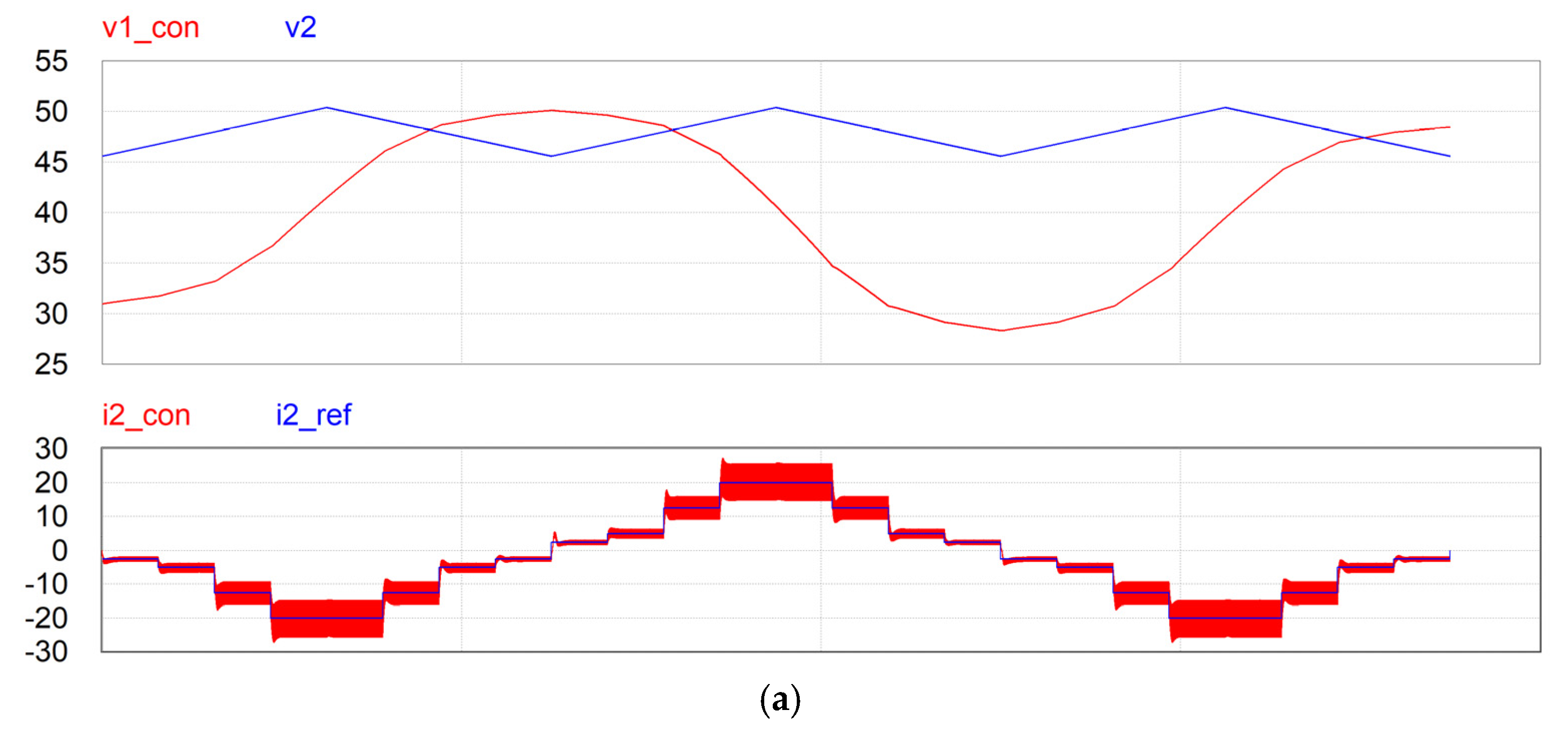
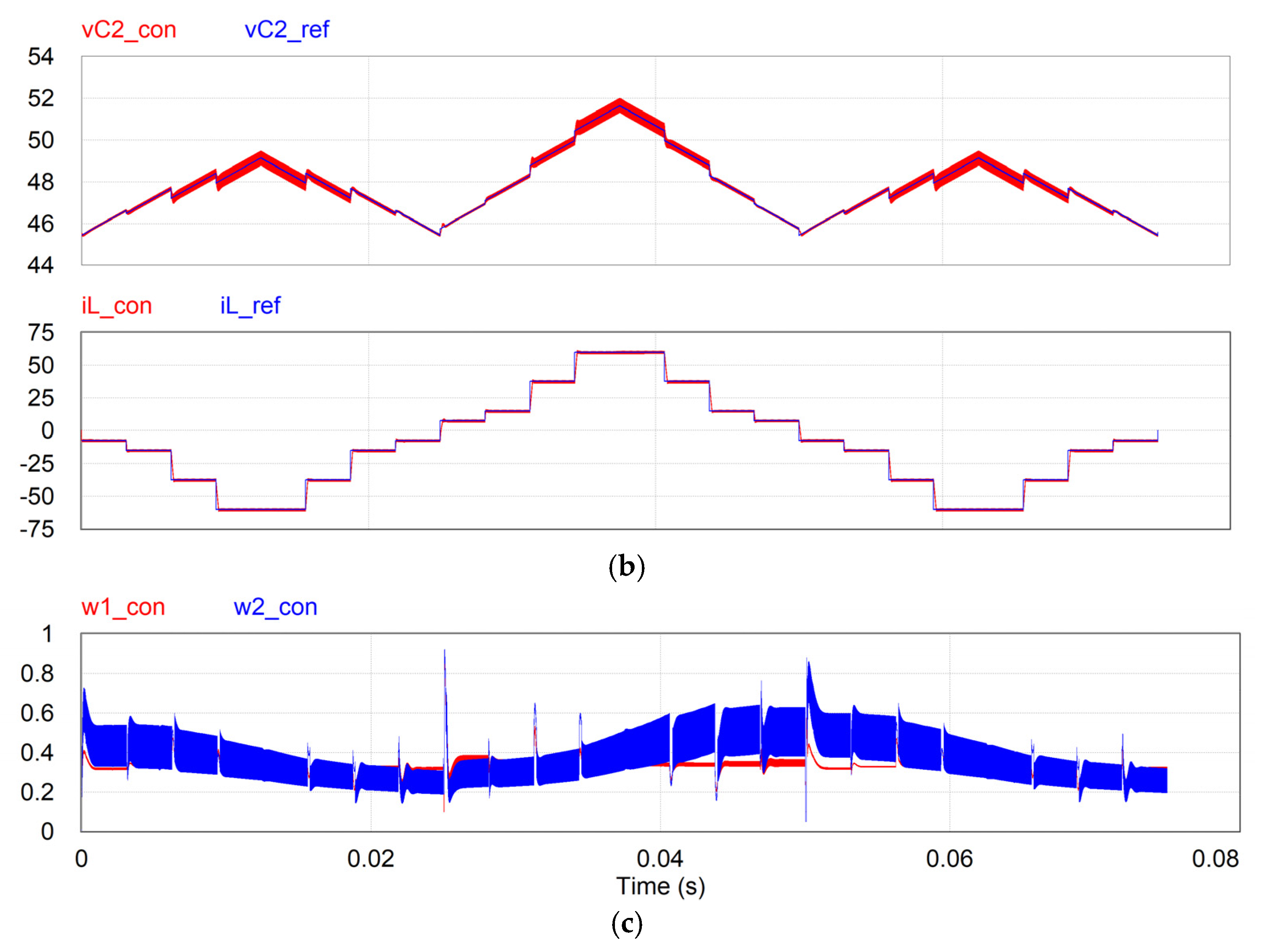
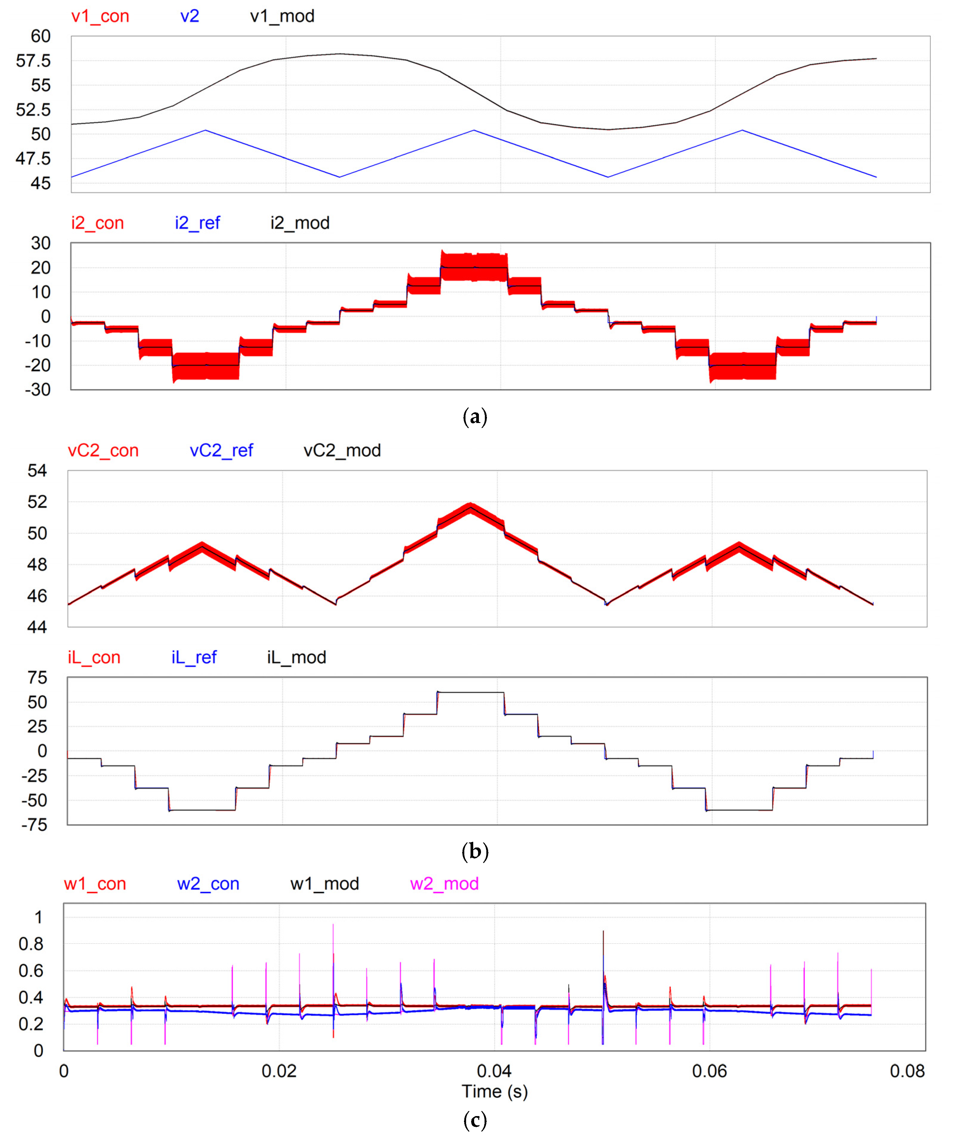
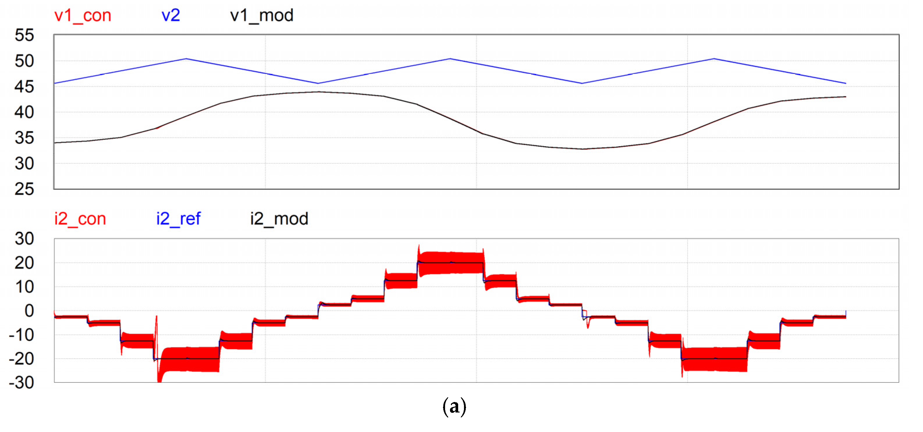
6. Performance Verification and Discussion

There are several aspects of the proposed concept to be verified. First is the performance achieved with the proposed control scheme with PI controllers and feedback linearization for various operating conditions: forward and reverse power flows with V1 < V2 and V1 > V2. This can be done with the mathematical equations derived in Section 3 and employing control variables w1 and w2. Next is the performance of the actual switched converter. The goal is to demonstrate that one can convert control variables w1 and w2, which are obtained for the unified model, into u1, u2, and u3 so that the converter operates in a desired mode. The dynamic response of the converter should be similar irrespectively of the selected mode of operation, as long as both w1 and w2 are used for obtaining u1, u2, and u3.
The schematic diagram of the proposed control scheme is shown in Figure 9. There, one can see how the control laws for w1 and w2 are created as a function of the reference signals and sensed converter quantities. LPFs are included to attenuate the switching harmonics, and a limiter is used to prevent the magnitude of iL, which is used in the denominator of (14), from becoming too small, during power flow reversals. Limiters are also used for keeping w1 and w2, which correspond to D3 and D1, within 0 and 1. Then, depending on the selected mode of operation, control variables, w1 and w2, are converted into the modulation signals u1, u2, and u3, and used in the PWM modulator of Figure 3 to create the gating signals for the switched converter.

6.1. Control Scheme with PI Controllers and Feedback Linearization

The performance of the proposed unified controller for multi-state operation of the bi-directional Buck–Boost DC-DC converter is verified with the mathematical model in this section. The parameters of the SC interface (V1 in Figure 1) are those shown in Section 5. An SC with a small capacitance (15 mF) is the base value used in this test so that one can observe the variations of the voltage in the storage unit (v1) as well as the fast varying current and voltage waveforms in the same time frame. It is assumed that the magnitude of the DC bus voltage and feeder (v2) and the value of the feeder impedance (R2) are known. They are used in the calculation of the reference value for the output capacitor voltage (vC2*) and inductor current (iL*) as a function of the reference injected current (i2*). As mentioned in Section 3.4, ki2L = 3.
Key waveforms obtained with control laws for w1 and w2, (14) and (18), and the mathematical model of the converter, (8)–(10), are shown in Figure 10. On the top, one can see the waveform of the DC bus voltage (v2), with an average value of 48 V and a +/−5% triangular ripple of 40 Hz along with the voltage across the SC (v1). The latter varies as a function of the injected current (i2), which is shown just below and concerns a staircase waveform of 20 Hz and a maximum current of 20 A. The voltage across the SC decreases when i2 > 0 and increases when i2 < 0. The injected power is shown in the screen at the bottom, presenting a zero average value. In such a case, the power losses across the two feeder resistors come from the SC, which tends to discharge over time, as seen in the top screen. For most of the time, v1 < v2, but v1 > v2 in a short segment. Therefore, the converter needs to operate in both the Boost (step-up) and Buck (step-down) modes. It is evident that there is good tracking of the reference values for the injected current (i2), output capacitor of the converter (vC2), and inductor current (iL), with control signals, w1 and w2, which are shown just below those waveforms.

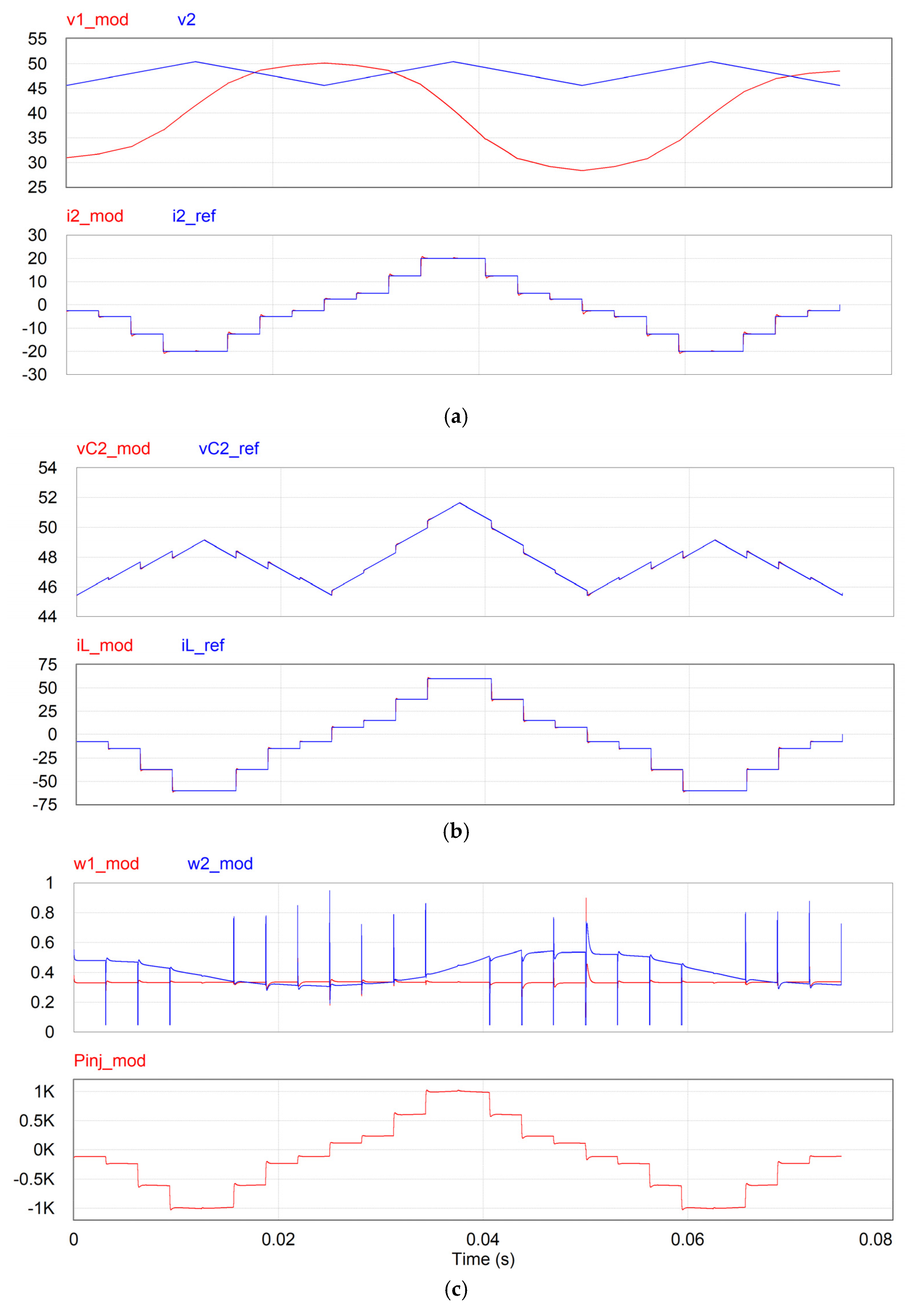
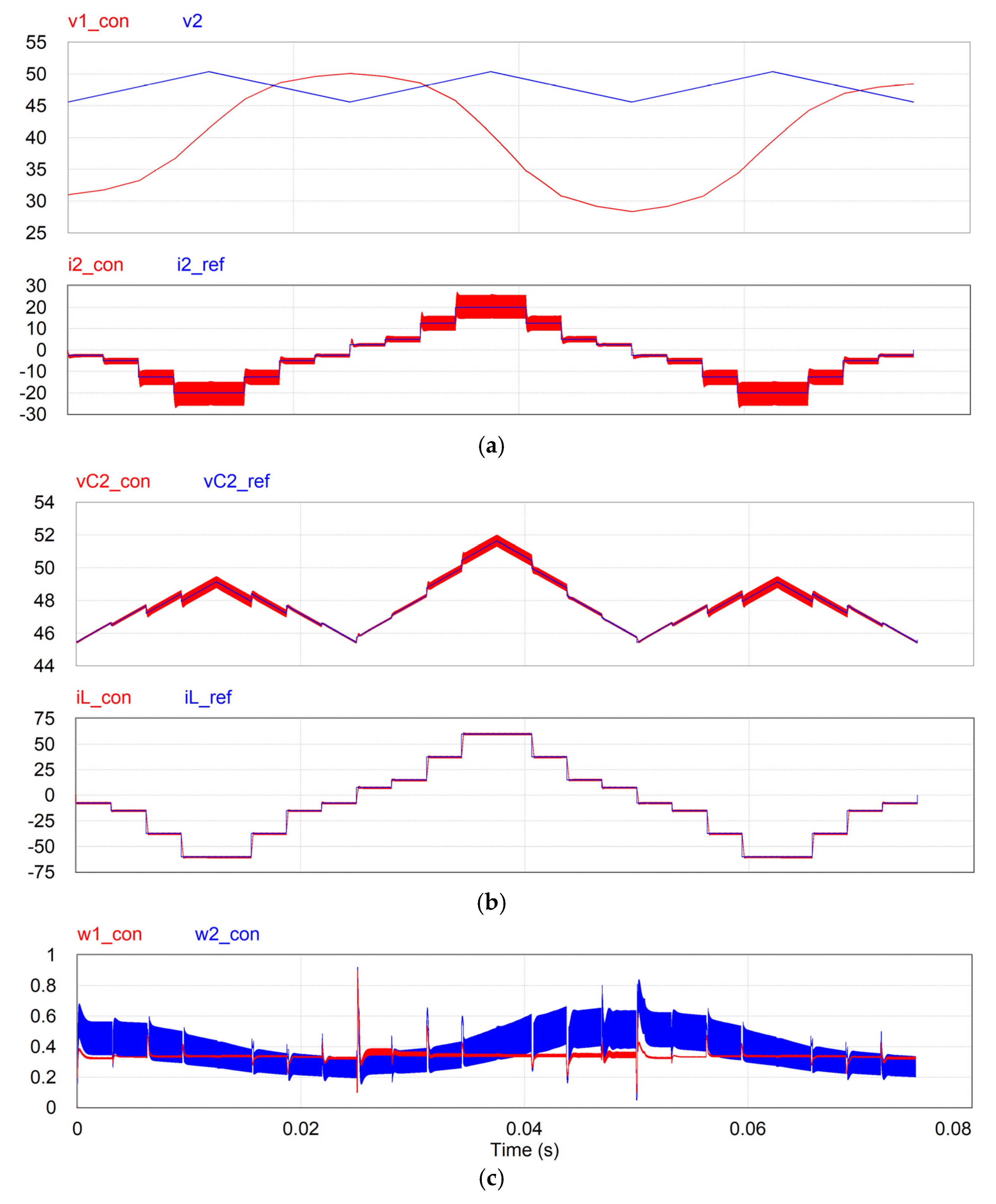
6.2. Simulation Results with the Switched Converter

Having shown that the proposed control scheme provides a fast and accurate control of the inductor and the output current of the converter using the developed mathematical model of the system, its feasibility is verified with the switched converter for the same test conditions. This is done by simulation with PSIM. In this case, the control variables (w1 and w2) are converted into the modulation signals of the PWM modulator (u1, u2, and u3) so that the converter operates in a desired multi-state mode according to the expressions shown in Table 2. Since the converter is expected to operate in the Buck and Boost modes, only the tri-state Buck–Boost and quad-state modes, in Table 2, are considered at first.
Figure 11 shows key waveforms for the switched converter operating in the quad-state mode. The waveforms are essentially the same obtained for the mathematical model test. The main difference is the presence of switching harmonics. Index “con” indicates results obtained with the switching converter, while “mod” refers to the mathematical model.
In Figure 12, one can see a close view of the control parameters (w1 and w2), the modulation signals (u1u2u3), and the gating signals of switches S1 and S3 for three switching cycles. There, one can observe all sorts of combinations of vgS1 and vgS3, meaning that all four switching states are employed in the quad-state mode.
Figure 13 shows the same waveforms for the switched converter operating in a tri-state Buck–Boost mode, mode 5 in Table 2. The waveforms are essentially the same as those for the quad-state mode. As shown in Figure 14, the free-wheeling mode, when S2 and S4 conduct together, is not present in this mode.
For testing the converter operating in the tri-state Buck and Boost modes, one should always have v1 > v2 and v1 < v2, respectively. In order to keep the same output voltage and current waveforms, one can change the initial voltage of the SC (v1) so that the converter always operates in the desired mode. It is important to reduce the range of variation of v1 by increasing the capacitance of the SC to 0.03 F. Figure 15 shows waveforms for the switched converter operating in the tri-state Buck mode, where v1 is always bigger than v2. Again, the unified controller allows a fast and close tracking of the reference quantities. The quantities obtained with the model, index “mod”, are shown along with those of the switched converter, index “con”, to show the similarities. The major difference is the presence of the switching harmonics that can be seen in some waveforms. The control parameters, modulation signals, and gating signals of switches are shown in Figure 16, where one can see that only three states are used, S13–S23–S24, as seen in Table 1.
Finally, Figure 17 shows waveforms for the switched converter operating in the tri-state Boost mode, where v1 is always smaller than v2. It should be noted that the conventional class-C converter DC-DC converter could not be used in this case. The unified controller allows a good tracking of the reference quantities. In the bottom screen, the control variables obtained for the switching converter, index “con”, are similar to those obtained for mathematical model, index “mod”. The control parameters, modulation signals, and gating signals of switches, with only three states, are shown in Figure 18. In this particular case, u2 = u3, as determined in Table 2.

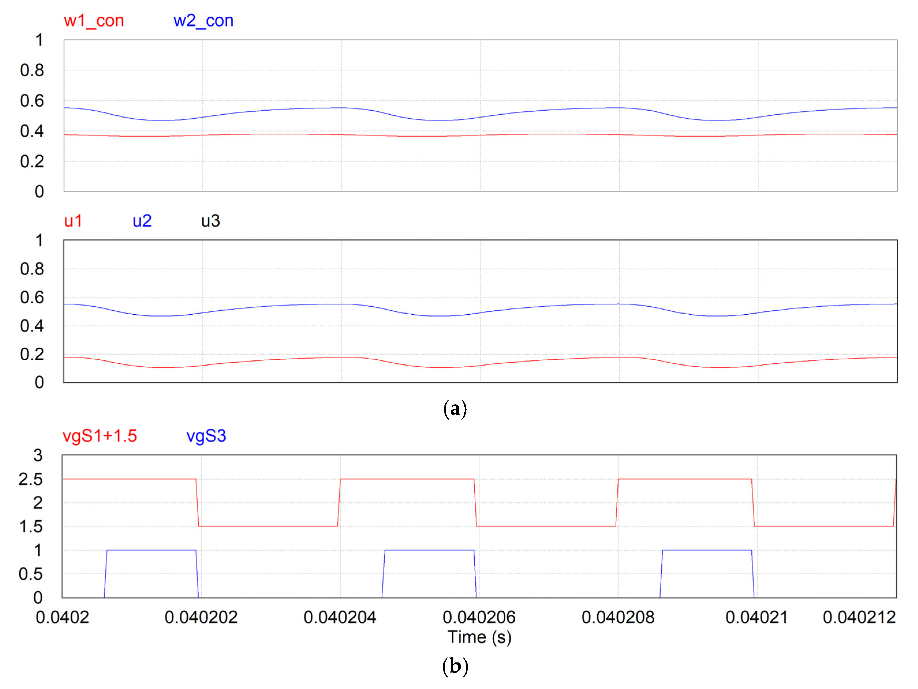
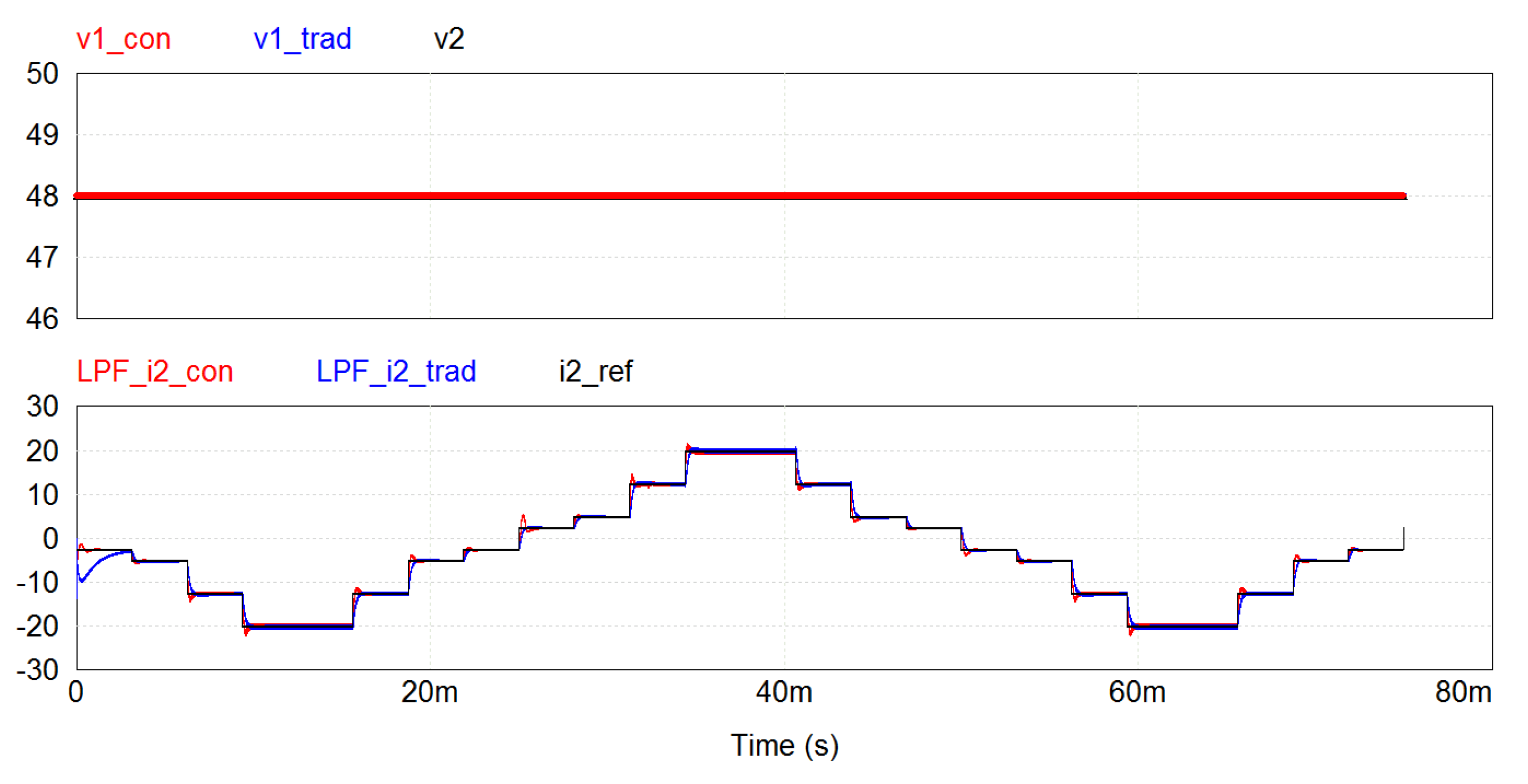
6.3. Comparison to a Conventional Technique

The performance of the proposed unified controller for multi-state operation will be compared with a conventional technique. In this case, it concerns the bi-directional DC-DC converter operating with dual state in the Buck–Boost mode (mode 2 in Table 1). The output current (i2) is controlled with a single loop employing a standard PI controller. This is designed considering a model of the plant linearized around a certain operating point. The transfer function relating the injected current (i2) to the duty cycle (D) of the converter is the following:
i 2 ( s ) D ( s ) = 1 R 2 L C 2 [ ( V C 1 + V C 2 ) ( I L L ) s s 2 + ( 1 R 2 C 2 ) s + ( 1 D ) 2 L C 2 ]
One can clearly see that the system presents a non-minimal phase when IL > 0. A linear PI controller was designed for the current loop considering VC1 = VC2 = 48 V, D = 0.5, and IL = 40 A. As a result of the RHP zero at 4.7 kHz, the bandwidth of the control loop should be about 20% of that; thus, it was selected as 1 kHz with a phase margin of 60°. A first-order LPF of 25 kHz was employed at the sensed output current signal. The parameters of the current loop PI controller are ki = 5.1 m, τi = 918 μs, and fpi = 5.8 kHz.
The conventional technique was used in the switched converter for the test case presented in Figure 12. The capacitance of the SC is 15 mF, and the DC-bus voltage (v2) presents an average value of 48 V and a +/−5% triangular ripple of 40 Hz. Figure 19 shows the SC voltage and the DC-bus voltage on the top. The screen at the bottom shows the staircase reference output current along with the current obtained with the proposed, index “con”, and the traditional, index “trad” control schemes. In this case, the filtered (25 kHz) output current signals are shown, so that one can better observe the difference between the two responses. There, one can see that the response of the traditional PI controller presents longer settling times than the proposed scheme, and sometimes, it fails to track the reference current. This is because the PI controller was designed for operation close to a certain operating point. Figure 20 shows the response of the two controllers when both the input and the output voltages are 48 V, which are the values used in the model of the plant and design of the traditional PI controller. There, one can see that the proposed and the conventional control techniques perform equally well.

6.4. Discussion

The first test shown in Section 6.1 for the bi-directional DC-DC converter interfacing the SC to a DC grid considered the mathematical model of the converter and the control laws for control variables w1 and w2. The resulting waveforms show that the proposed control scheme with multi-variable control and feedback linearization provides a very good transient response to step variations in the reference currents i2* and iL*. In addition, the load disturbance, represented by the triangular voltage ripple on the DC bus, did not degrade the tracking of currents nor output voltage in steady state. The dynamic responses with fixed PI controllers were essentially the same, despite the large variation in the SC voltage, 28 to 50 V, and the reversal of the power flow direction. This is provided by the feedback linearization technique.
The second test shown in Section 6.2 considered the actual/switched bi-directional DC-DC converter, with the scheme for converting control variables w1 and w2, into PWM modulation signals u1, u2, and u3, according to a selectable and desired multi-state mode of operation. The quad-state and tri-state Buck–Boost modes were used for the cases where the input voltage is smaller and larger than the output voltage. For the test with the tri-state Buck and tri-state Boost modes, the values of the SC and initial input voltage were adjusted so that the input voltage is always larger for the Buck and smaller for the Boost than the output or DC grid voltage, considering the same reference output current and DC bus voltage. It should be noted that taking into account all these tests, the input voltage varied between 28 and 58 V, but the dynamic response of the proposed control scheme with fixed PI controllers was essentially the same for all multi-state modes of operation.
The fact that the conventional current control scheme for a dual-state Buck–Boost DC-DC converter with a single PI controller works well when the operating conditions do not vary much was highlighted in Section 6.3. There, it was shown that in applications such as the interface of a SC, with a wide voltage variation, to an unregulated DC grid, the use of the proposed unified controller provides a better response in terms of dynamic response and tracking of the reference output current.

7. Conclusions

This paper presented a unified controller for multi-state operation of a bi-directional Buck–Boost DC-DC converter suitable for interfacing supercapacitors (SCs) to DC grids. According to the literature, the multi-state operation of DC-DC converters allows the elimination of Right Half Plane (RHP) zeros, switch power loss equalization, etc. The challenge of multi-variable control was tackled by employing feedback linearization and simple fixed PI controllers. A mathematical model for designing the controllers and obtaining the control laws for the generic parameters (w1 and w2) was developed. These can be converted to three modulation signals (u1, u2, and u3) and used in a carrier-based PWM scheme for generating the gating signals for five different multi-state modes of operation. The technique was verified by means of simulations in the interface of a SC operating in a wide range of voltages to a DC bus with a +/−5% of voltage ripple. The same set of controllers provided fast and accurate regulation for step changes in the reference quantities under bi-directional power flow for the converter operating in quad-state, tri-state Buck–Boost, tri-state Buck, and tri-state Boost modes.

Author Contributions

Conceptualization, G.R.B., G.D., W.P.-L. and L.A.C.L.; methodology, G.D., W.P.-L. and L.A.C.L.; software, G.R.B. and L.A.C.L.; validation, G.R.B., G.D., W.P.-L. and L.A.C.L.; formal analysis, G.D. and W.P.-L.; investigation, G.R.B., G.D., W.P.-L. and L.A.C.L.; resources, G.D. and L.A.C.L.; data curation, G.R.B. and L.A.C.L.; writing—original draft preparation, G.R.B. and L.A.C.L.; writing—review and editing, G.R.B., G.D., W.P.-L. and L.A.C.L.; visualization, G.R.B. and L.A.C.L.; supervision, G.D and L.A.C.L.; project administration, G.D. and L.A.C.L.; funding acquisition, G.D. and L.A.C.L. All authors have read and agreed to the published version of the manuscript.

Funding

This research was funded by the Natural Sciences and Engineering Research Council (NSERC) of Canada.

Institutional Review Board Statement

Not applicable.

Informed Consent Statement

Not applicable.

Conflicts of Interest

The authors declare no conflict of interest.

References

  1. Ferahtia, S.; Djeroui, A.; Mesbahi, T.; Houari, A.; Zeghlache, S.; Rezk, H.; Paul, T. Optimal Adaptive Gain LQR-Based Energy Management Strategy for Battery–Supercapacitor Hybrid Power System. Energies 2021, 14, 1660. [Google Scholar] [CrossRef]
  2. Viswanathan, K.; Oruganti, R.; Srinivasan, D. A novel tri-state boost converter with fast dynamics. IEEE Trans. Power Electron. 2002, 17, 677–683. [Google Scholar] [CrossRef]
  3. Georgious, R.; Garcia, J.; Sumner, M.; Saeed, S.; Garcia, P. Fault Ride-Through Power Electronic Topologies for Hybrid Energy Storage Systems. Energies 2020, 13, 257. [Google Scholar] [CrossRef] [Green Version]
  4. Saeed, S.; Lopes, L.A. Fault Protection Scheme for DC Nanogrids Based on the Coordination of Fault-Insensitive Power Electronic Interfaces and Contactors. In Proceedings of the IECON 2019—45th Annual Conference of the IEEE Industrial Electronics Society, Lisbon, Portugal, 14–17 October 2019; pp. 5789–5794. [Google Scholar]
  5. Waffler, S.; Kolar, J.W. An Enhanced Control Algorithm for Improving the Light-Load Efficiency of Noninverting Synchronous Buck-Boost Converters. IEEE Trans. Power Electron. 2016, 31, 3395–3399. [Google Scholar]
  6. Kim, D.-H.; Lee, B.-K. A Novel Low-Loss Modulation Strategy for High-Power Bidirectional Buck + Boost Converters. IEEE Trans. Power Electron. 2009, 24, 1589–1599. [Google Scholar]
  7. Tsai, Y.-Y.; Tsai, Y.-S.; Tsai, C.-W.; Tsai, C.-H. Digital Noninverting Buck-Boost Converter with Enhanced Duty-Cycle-Overlap Control. IEEE Trans. Circuits Syst.-II Express Briefs 2017, 64, 41–45. [Google Scholar] [CrossRef]
  8. Jones, D.C.; Erickson, R.W. Buck-Boost Converter Efficiency Maximization via a Nonlinear Digital Control Mapping for Adaptive Effective Switching Frequency. IEEE J. Emerg. Sel. Top. Power Electron. 2013, 1, 153–165. [Google Scholar] [CrossRef]
  9. Choubey, A.; Lopes, L.A.C. A Tri-State 4-Switch Bi-Directional Converter for Interfacing Supercapacitors to DC Micro-Grids. In Proceedings of the PEDG 2017—8th International Symposium on Power Electronics for Distributed Generation Systems, Florianopolis, Brazil, 17–20 April 2017; pp. 1–6. [Google Scholar]
  10. He, M.; Zhang, F.; Xu, J.; Yang, P.; Yan, T. High Efficiency Two-Switch Tri-State Buck-Boost Power Factor Correction Converter with Fast Dynamic Response and Low-Inductor Current Ripple. IET Power Electron. 2013, 6, 1544–1554. [Google Scholar] [CrossRef]
  11. Viswanathan, K.; Oruganti, R.; Srinivasan, D. A Dual-Mode Control of Tri-state Boost Converter for Improved Performance. IEEE Trans. Power Electron. 2005, 20, 790–797. [Google Scholar] [CrossRef]
  12. Aharon, I.; Kuperman, A.; Shmilovitz, D. Analysis of Dual-Carrier Modulator for Bidirectional Noninverting Buck-Boost Converter. IEEE Trans. Power Electron. 2015, 30, 840–848. [Google Scholar] [CrossRef]
  13. Luo, X.; Barreras, J.V.; Chambon, C.L.; Wu, B.; Batzelis, E. Hybridizing Lead–Acid Batteries with Supercapacitors: A Methodology. Energies 2021, 14, 507. [Google Scholar] [CrossRef]
  14. Gheisarnejad, M.; Farsizadeh, H.; Tavana, M.-R.; Khooban, M.H. A Novel Deep Learning Controller for DC–DC Buck–Boost Converters in Wireless Power Transfer Feeding CPLs. IEEE Trans. Ind. Electron. 2021, 68, 6379–6384. [Google Scholar] [CrossRef]
  15. Boutebba, O.; Semcheddine, S.; Krim, F.; Corti, F.; Reatti, A.; Grasso, F. A Nonlinear Back-stepping Controller of DC-DC Non Inverting Buck-Boost Converter for Maximizing Photovoltaic Power Extraction. In Proceedings of the EEEIC/I&CPS Europe 2020—IEEE International Conference on Environment and Electrical Engineering and IEEE Industrial and Commercial Power Systems Europe, Madrid, Spain, 9–12 June 2020; pp. 1–6. [Google Scholar]
  16. Iovine, A.; Carrizosa, M.J.; Damm, G.; Alou, P. Nonlinear Control for DC Microgrids Enabling Efficient Renewable Power Integration and Ancillary Services for AC Grids. IEEE Trans. Power Syst. 2019, 34, 5136–5146. [Google Scholar] [CrossRef]
  17. Perez, F.; Iovine, A.; Damm, G.; Galai-Dol, L.; Ribeiro, P.F. Stability Analysis of a DC MicroGrid for a Smart Railway Station Integrating Renewable Sources. IEEE Trans. Control. Syst. Technol. 2020, 28, 1802–1816. [Google Scholar] [CrossRef]
  18. Li, X.; Chen, X. A Multi-Index Feedback Linearization Control for a Buck-Boost Converter. Energies 2021, 14, 1496. [Google Scholar] [CrossRef]
  19. Callegaro, L.; Ciobotaru, M.; Pagano, D.J.; Fletcher, J.E. Feedback Linearization Control in Photovoltaic Module Integrated Converters. IEEE Trans. Power Electron. 2019, 34, 6876–6889. [Google Scholar] [CrossRef]
  20. Mohan, N.; Undeland, T.M.; Robbins, W.P. Power Electronics: Converters, Applications and Design, 3rd ed.; John Wiley & Sons: Hoboken, NJ, USA, 2002. [Google Scholar]
  21. Mohan, N. Power Electronics: A First Course, 1st ed.; Wiley: Hoboken, NJ, USA, 2011. [Google Scholar]
Figure 1. The non-isolated bi-directional Buck–Boost DC-DC converter.
Energies 14 07921 g001
Figure 2. The proposed carrier-based PWM modulation scheme: (a) Carrier and modulation signals; (b) Gating signals of the switches; (c) States of operation.
Energies 14 07921 g002
Figure 3. Realization of the proposed carrier-based PWM modulation scheme for the non-isolated bi-directional Buck–Boost DC-DC converter.
Energies 14 07921 g003
Figure 4. Block diagram with the auxiliary variable vx used for the design of the output voltage controller.
Energies 14 07921 g004
Figure 5. Block diagram with the auxiliary variable vy used for the design of the inductor current controller.
Energies 14 07921 g005
Figure 6. Equivalent circuit of the converter with sources and resistances reflected to the intermediate (inductor) segment.
Energies 14 07921 g006
Figure 7. Values of w2 as a function of i2 and V1, for V2 = 48 V, iL = 40 A, and R1 = R2 = 62.5 mΩ. Values of V1 are 18 V (green), 20.17 V (blue), 24 V (black), V1min = 27.125 V (red), and 32 V (magenta).
Energies 14 07921 g007
Figure 8. Values of w2 as a function of i2 and V1, for V2 = 48 V, iL = 60 A, and R1 = R2 = 62.5 mΩ. Values of V1 are: 18 V (green), 20.17 V (blue), 24 V (black), V1min = 27.125 V (red), and 32 V (magenta).
Energies 14 07921 g008
Figure 9. Proposed unified controller for multi-state operation of the bi-directional Buck–Boost DC-DC converter.
Energies 14 07921 g009
Figure 10. Waveforms with the mathematical model: (a) The top plot shows the input and output voltages (in Volts), while the bottom one presents the reference and output current (in Amps); (b) The top plot shows the reference and output capacitor voltage (in Volts), while the bottom one presents the reference and inductor current (in Amps); (c) Top plot shows the control variables, while the bottom one presents the injected power (in Watts).
Energies 14 07921 g010
Figure 11. Waveforms with the switched converter in the quad-state mode: (a) The top plot shows the input and output voltages (in Volts), while the bottom one presents the reference and output current (in Amps); (b) The top plot shows the reference and output capacitor voltage (in Volts), while the bottom one presents the reference and inductor current (in Amps); (c) Control variables.
Energies 14 07921 g011
Figure 12. Waveforms with the switched converter in the quad-state mode: (a) Top plot shows the control variables while the bottom one presents the modulation signals; (b) Gating signals of switches S1 and S3.
Energies 14 07921 g012
Figure 13. Waveforms with the switched converter in the tri-state Buck–Boost no free-wheeling mode: (a) Top plot shows the input and output voltages (in Volts), while the bottom one presents the reference and output current (in Amps); (b) Top plot shows the reference and output capacitor voltage (in Volts), while the bottom one presents the reference and inductor current (in Amps); (c) Control variables.
Energies 14 07921 g013aEnergies 14 07921 g013b
Figure 14. Waveforms with the switched converter in the tri-state Buck–Boost no free-wheeling mode. (a) Top plot shows the control variables, while the bottom one presents the modulation signals; (b) Gating signals of switches S1 and S3.
Energies 14 07921 g014
Figure 15. Waveforms with the switched converter in the tri-state Buck mode: (a) The top plot shows the input and output voltages (in Volts) while the bottom one presents the reference and output current (in Amps); (b) Top plot shows the reference and output capacitor voltage (in Volts), while the bottom one presents the reference and inductor current (in Amps); (c) Control variables for the model and switching converter.
Energies 14 07921 g015
Figure 16. Waveforms with the switched converter in the tri-state Buck mode: (a) Top plot shows the control variables while the bottom one presents the modulation signals; (b) Gating signals of switches S1 and S3.
Energies 14 07921 g016
Figure 17. Waveforms with the switched converter in the tri-state Boost mode: (a) Top plot shows the input and output voltages (in Volts), while the bottom one presents the reference and output current (in Amps); (b) Top plot shows the reference and output capacitor voltage (in Volts), while the bottom one presents the reference and inductor current (in Amps); (c) Control variables for the model and switching converter.
Energies 14 07921 g017aEnergies 14 07921 g017b
Figure 18. Waveforms with the switched converter in the tri-state Boost mode: (a) Top plot shows the control variables while the bottom one presents the modulation signals; (b) Gating signals of switches S1 and S3.
Energies 14 07921 g018
Figure 19. Waveforms with the proposed unified multi-state controller and the traditional dual-state Buck–Boost controller for the SC interface to a DC grid: The top plot shows the input and output voltages (in Volts) for the two cases, while the bottom one presents the reference and output currents (in Amps) for the two cases.
Energies 14 07921 g019
Figure 20. Waveforms with the proposed unified multi-state controller and the traditional dual-state Buck–Boost controller for two 48V regulated DC-buses: The top plot shows the input and output voltages (in Volts) for the two cases, while the bottom one presents the reference and output currents (in Amps) for the two cases.
Energies 14 07921 g020
Table 1. Modes of operation.
u1u2u3 StatesMode of Operation
00u3S23–S24Not useful—Disregard
0u2,3u2,3S13–S24Not useful—Disregard
0u21S13–S231—Dual-State Buck
u1,2u1,21S14–S232—Dual-State Buck–Boost
u111S14–S133—Dual-State Boost
0u2u3S13–S23–S244—Tri-state Buck with free-wheeling (fw)
u1u21S14–S13–S235—Tri-state Buck–Boost with no fw
u1u2,3u2,3S14–S13–S246—Tri-state Boost with fw (u2,3u1)
u1,2u1,2u3S14–S23–S247—Tri-state Buck–Boost with fw (u3u1,2)
u1u2u3S14–S13–S23–S248—Quad-state
Table 2. Multi-state modes of operation compatible with the proposed control scheme.
u1u2u3Mode of Operation
0w2w14—Tri-state Buck with free-wheeling (fw)
1-w1w2 1 5—Tri-state Buck–Boost with no fw
w2-w1w2w26—Tri-state Boost with fw
w2w2w2 + w17—Tri-state Buck–Boost with fw
c-w1w2c8—Quad-state
Publisher’s Note: MDPI stays neutral with regard to jurisdictional claims in published maps and institutional affiliations.

