1. Introduction
Power MOSFETs are semiconductor devices that are commonly used in electronic circuits. As a result of the current flowing through semiconductor devices and power losses, the temperature of the die of these devices increases over the ambient temperature [
1,
2]. This phenomenon is called self-heating [
3]. The temperature of the die of the semiconductor device may also increase as a result of heat dissipation in the other device and the conduction of this heat, e.g., due to placing both devices on the same heat sink, namely thermal coupling [
4,
5].
The parameters that are used to characterize the thermal phenomena in electronic devices is transient thermal impedance
Zth(
t), and, in the case of simplification of an analysis to the steady state, thermal resistance
Rth [
6,
7].
The knowledge of transient thermal impedance allows computations of a waveform of the chip temperature at a known waveform of the power
p(
t) that is dissipated in this device [
1,
8,
9,
10]. According to the classical theory [
1,
7,
11] the device internal temperature of a discrete semiconductor device can be computed using the following formula.
where
Ta denotes the ambient temperature,
p(
t) is the waveform of the power that is dissipated in this device, whereas
Z’th(
t) is a time derivative of its transient thermal impedance. It is worth underlining that for semiconductor devices that are operating in power electronic networks, the waveforms
p(
t) and
Tj(
t) are periodical functions at the steady state [
12,
13]. Of course, the shape of the waveform
p(
t) does not influence the value of temperature
Tj at the steady state, which mostly depends on the mean value of the dissipated power [
14].
In the case of a discrete device, transient thermal impedance is defined with the formula [
15,
16].
where
Tj(
t) denotes the waveform of the chip temperature,
Ta—the ambient temperature and
P is the amplitude of the step of the power that is dissipated in this device. The value of transient thermal impedance
Zth(
t) at
t → ∞ is equal to thermal resistance
Rth.
In turn, in the case of thermal coupling between the devices “
i” and “
k”, mutual transient impedance is defined with the formula [
10].
where
Tji denotes the temperature of the device “
i” and
Pk the amplitude of the step of the power that is dissipated in the device “
k”.
Both transient thermal impedance and thermal resistance may be determined by measurements or computations using the finite element method (FEM) in the determined device working conditions [
11,
17,
18].
The measurements of the values of thermal parameters may be performed using contact methods, optical methods, or electrical methods [
15,
19].
The contact methods most often use the dependence of resistance (resistance temperature detectors—RTDs), or thermoelectric potential (thermocouples—TCs) of a temperature sensor. Such sensors must stay in touch with the surface, the temperature of which is measured.
In turn, the optical methods are based on a variation of an optical parameter with the temperature. The most frequently used optical parameter, due to common availability of dedicated commercial measurement instrumentation (thermal cameras, pyrometers), is the intensity of infrared radiation [
15,
19].
In a typical case, when the chips are encapsulated in packages, the disadvantage of the contact and the optical methods is that only the temperature of the package surface T
c can be measured. This temperature may be much lower than the chip temperature
Tj and as a result, the values of the thermal parameters that are obtained with these methods may be underestimated [
20].
The method that is recommended by the standardisation institutions [
15,
16] for the measurement of thermal parameters of semiconductor devices is, so called, the indirect electrical method. This method is based on the use of an electrical thermo-sensitive parameter (TSP), the value of which varies with changes of the chip temperature.
For power MOSFETs, the following TSPs are used [
21,
22]:
- (a)
vGS voltage at a selected value of drain current iD for the transistor that is operating in the saturation range,
- (b)
vF voltage on the forward-biased body diode at a selected value of this forward current,
- (c)
vDS voltage between the drain and the source of the transistor that are operating in a linear range at a selected value of the drain current.
Carrying out the measurements of thermal parameters with the electrical method requires, among other things, the measurements of the thermometric characteristic, i.e., the dependence binding the selected TSP with the chip temperature—TSP(T
j) and next finding a function approximating this dependence. In the literature, for the approximation (modelling) of the TSP(T
j) dependence, the linear function is commonly applied [
2,
15,
16].
The paper [
21] shows the advantages of using selected TSPs of the power MOS transistor, whereas the paper [
14] shows the influence of the selection of the TSP of the IGBT on the accuracy of determining its internal temperature. On the other hand, in [
22] it is shown that the non-uniformity of the temperature distribution in the semiconductor die of the power MOS transistor may exceed even 50 K and the justifiability of using a compact thermal model of this device is discussed.
In the known literature, the lack of a systematic analysis of the typically used measurement methods of thermal parameters of semiconductor devices is observed. Typically used simplifications can strongly limit the accuracy of these methods.
In this paper, the selected problems that are related to the measurements of thermal parameters of power MOSFETs placed on a common heat sink are analysed. The application of the indirect electrical method, the contact method, and the optical method in measuring self and transfer transient thermal impedances of these transistors is presented. The measurement errors of each of the considered methods are formulated. For the indirect electrical methods, the influence of the selection of TSPs and the function approximating thermometric characteristics on the measurement error are taken into consideration. Some results that illustrate the influence of the used measurement method on the obtained waveforms of transient thermal impedances are presented and discussed.
The investigated MOSFETs that were coupled thermally via a common heat sink are described in
Section 2. The methods and the setups for measuring the thermal parameters of the investigated transistors with the electrical method are described in
Section 3. In
Section 4, the problem of credible measurements and approximation of thermometric characteristics of the investigated transistors is analysed. In
Section 5 the measurement error of thermal resistance in each of the considered measurement methods is analysed. The exemplary results of the measurements of self and mutual transient thermal impedances of the investigated MOSFETs are presented and discussed in
Section 6.
4. Measurement and Approximation of Thermometric Characteristics
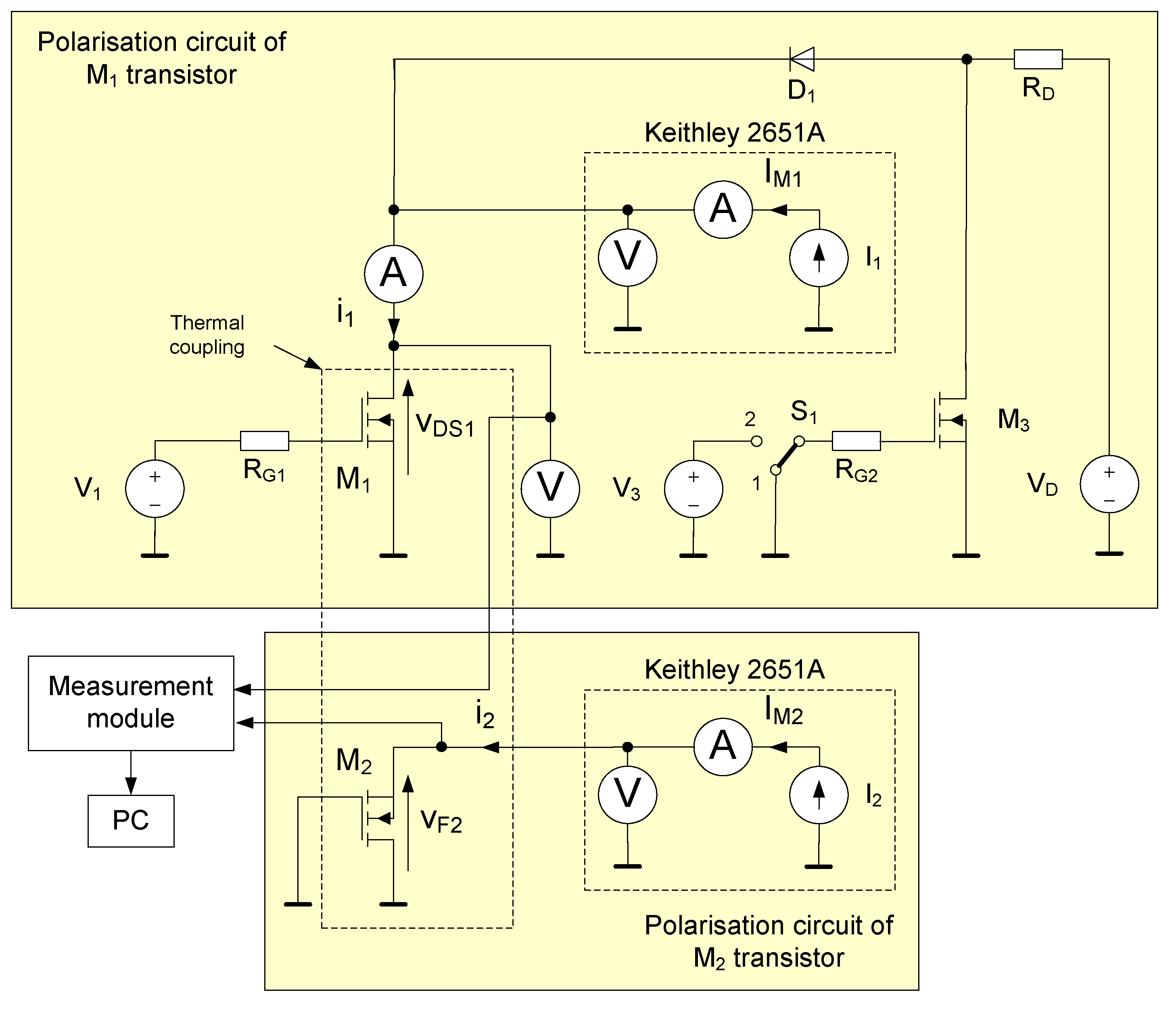
Using the measurement setups that are shown in
Figure 2,
Figure 3 and
Figure 4, the thermometric characteristics of transistor M
1 operating at various values of current I
M were measured. The results of the measurements are shown in the
Figure 5,
Figure 6 and
Figure 7. The measurement points are marked with dots and the approximating functions with lines. The solid and dashed lines were applied for the quadratic and the linear approximating functions, respectively.
Figure 5 illustrates the thermometric characteristics v
F(T
j) of transistor M
1 that were measured at selected values of the forward current of the body diode I
F = I
M.
As it is seen, the measured characteristics are slightly nonlinear in the temperature range from 20 to 140 °C for all the considered IM current values ranging from 1 mA to 20 mA. Quadratic and linear approximation lines are almost indistinguishable. The slope of the linear approximating function varies from −2.2 mV/°C for IM = 20 mA to −2.5 mV/°C at IM = 1 mA.
In turn,
Figure 6 shows the thermometric characteristics v
DS(T
j) that were measured in the setup shown in
Figure 2 at selected values of the drain current i
D = I
M and v
GS = 15 V.
As it is seen, the measured dependences v
DS(T
j) are nonlinearly increasing functions. The slope of the considered characteristics strongly depends on the drain current value I
M. The slope of the linear approximating function increases from about 0.4 mV/°C for I
M = 50 mA to about 2.45 mV/°C for I
M = 0.3 A. It is worth noticing that the measured v
DS voltage values at the considered I
M current values are low and therefore may be susceptible to interference. Obtaining the value of v
DS ranging in several hundred millivolts requires the measurement current of at least 0.2 A. The value of this current should be selected depending on the resistance R
DS(on), which for the transistor under consideration is 0.85 Ω at T
a = 25 °C and increases with the temperature to 1.95 Ω at T
a = 150 °C [
23].
RDS(on) of many contemporary power MOS transistors is even several hundred times lower, which means that the desired vDS voltage value can be obtained only with IM current of even several dozen amperes. This can be a significant technical problem when a voltage drop on the resistance of the channel of the turned on transistor vDS is used to measure the thermal resistance of MOSFETs.
Figure 7 shows the thermometric characteristics v
GS(T
j) that were measured at selected values of the drain current i
D = I
M and the fixed value of the drain-source voltage v
DS = 7 V (
Figure 7a) and v
DS = 20 V (
Figure 7b), respectively.
As can be seen in
Figure 7a, at a low value of voltage v
DS, the thermometric characteristics at the same drain current correspond to a higher v
GS value. It is related to the intuitively obvious situation when an increase in the drain current requires an increase in voltage v
GS. The slope of the linear approximation of v
GS(T
j) characteristics is a decreasing function of current i
D and varies from −6.6 mV/°C, at I
M = 1 mA to −4.9 mV/°C, at I
M = 0.1 A.
In turn, in
Figure 7b, the results at a higher value of voltage v
DS = 20 V are shown. The influence of current i
D on voltage v
GS at the fixed temperature is described by a function having the maximum at I
M = 10 mA. The measured dependences v
GS(T
j) are monotonically decreasing functions and the slope of their linear approximation decreases from −6.6 mV/°C at I
M = 1 mA to −2.4 mV/°C at I
M = 50 mA. The observed influence of the drain current on the considered thermometric characteristics for currents I
M > 10 mA may be caused by a self-heating phenomenon. For the low values of current i
D (i
D ≤ 10 mA), the investigated transistor operates in the sub-threshold range, whereas for higher values of this current—in the saturation range. As it is clear from, e.g., the papers [
33,
34] for a transistor operating in the sub-threshold range, that the dependence i
D(v
GS) resulting from self-heating is an ambiguous relation.
In the paper [
35], it is shown that an important influence on the characteristics v
GS(T
j)@I
M = const has the value of voltage v
DS. For example, for the IRF 840 transistor the values of voltage v
GS at a selected value, the drain current and the temperature differ between each other even by 1 V at voltage v
DS changes by 5 V. These differences are particularly visible at higher values of the drain current (exceeding several dozen mA). At low values of this current (up to 10 mA), the voltage v
DS has practically no influence on the characteristics under consideration.
From amongst the characteristics that are shown in
Figure 5,
Figure 6 and
Figure 7, one was selected for each TSP. In the case of v
F for further consideration, the characteristic that was measured at current I
M = 1 mA was selected. In the case of v
DS, the characteristic that was measured at I
M = 0.3 A and v
GS = 15 V was chosen. In the case of v
GS, the characteristic that was measured at I
M = 5 mA was selected, which is identical at the changes of v
DS in a wide range. The independence of v
GS on v
DS changes is important because, in the setup shown in
Figure 3, after the switchover of transistor M
1 from the heating stage to the measurement stage, its v
DS voltage shifts by several volts. In the case when the characteristics for various v
DS were not the same, the additional error that is related to a change of the slope of the thermometric characteristic would appear.
From the literature it appears that thermometric characteristics are typically approximated with linear functions [
2,
16]. Due to the nonlinearity of the measured dependences, TSP(T
j), such approximation may be a source of error.
As it is seen in
Figure 5,
Figure 6 and
Figure 7, the measured dependences can be approximated with good accuracy with a polynomial of the second order. In
Figure 8, the dependences of the difference of the transistor M
1 die temperature were computed with the linear T
jl and the quadratic approximation of selected characteristics for further measurements, referring to the same chip temperature T
j for all the three considered TSPs, are presented.
The temperature
Tjl was computed from the formula
and
Tjq from the formula
In both of the formulas, the TSP denotes the value of a thermal parameter, hence a1, b1, a2, b2, and c2 are the coefficients of the functions approximating the dependences Tj(TSP).
To illustrate the dependence of the difference, Tjl–Tjq form all the TSPs that are being considered on the transistor M1 die temperature in a single figure, a variable of the x-axis was swapped from the TSP to Tj. To obtain that, it was assumed that as a result of dissipation of the power equal to 25 W in transistor M1 in the ambient temperature 20 °C, the transistor temperature increased to 145 °C. The value of Rth that was calculated at such assumptions is equal to 5 K/W.
As is seen in
Figure 8, the biggest differences between the chip temperature that were calculated using the linear and the quadratic approximations occurred in the middle and at the extremes of the considered temperature range and are directly related to the nonlinearity of the dependence TSP(T
j). In the case of v
F the difference is below 1 °C, but in the case of v
DS, it reaches 6.5 °C at the chip temperature 145 °C.
In turn, in the case of the measurements of transient thermal impedance and thermal resistance, the value of an increase of the die temperature over the ambient temperature Δ
Tj has an important influence. In
Figure 9 the difference of an increase of the chip temperature over the ambient temperature that is calculated at the linear Δ
Tjl and the quadratic Δ
Tjq approximations of the thermometric characteristics for the same conditions as for the case in
Figure 7 is shown.
The value of an increase of the chip temperature over the ambient temperature in the case of the linear approximation was computed from the formula
and in the case of the quadratic approximation form the formula
where
TSPa denotes the
TSP value at temperature
Ta.
As it is seen, the value of the difference of the temperature Δ
Tjl − Δ
Tjq that is being considered is the biggest at
Tj = 90 °C. In the case of selection of v
F as a TSP, this difference does not exceed 1 °C, for v
GS it is equal to 5 °C and for v
DS it reaches 8.5 °C. The conclusion from the presented analysis is that the selection of the approximating function may have an important influence on the measured value of the MOSFET transistor chip temperature whilst the indirect electrical method is applied. The use of the linear approximation for the nonlinear dependence of v
DS(T
j)@I
M = const may cause an underestimation of the measured increase of the temperature
Tj over the ambient temperature
Ta even by 8.5 °C and as a result the underestimation of the value of
Zth(t) and
Rth. The differences between the obtained results of estimation values of the devices internal temperature using the linear and quadratic approximation of thermometric characteristics result from the nonlinearity of these characteristics that are visible in
Figure 5,
Figure 6 and
Figure 7.
5. Analysis of the Measurement Error
One of the features of the measurement method in deciding about its applicability is the measurement error. In this section the influence of selected factors on the measurement error of the power MOSFETs thermal resistance carried out using the methods that are described in the
Section 3 is analysed.
The measurement error of thermal resistance can be calculated using the complete differential method [
20] in relation to the Formula (2). In such a case, the dependence describing the absolute measurement error of
Rth is obtained
and the relative error of the measurement is given by the formula
As it results from the Formula (10), the absolute value of the thermal resistance measurement is reversely proportional to the value of an increase in the die temperature over the ambient temperature and to the power that is dissipated in the transistor, causing this temperature increase.
The measurement error Δ
P of the power is identical for each of the considered measurement methods and with the appropriate selection of measuring instruments, it does not exceed 0.1% of the measured value of the power
P [
20]. In turn, the error in the measurements of the internal temperature Δ
Tj is different for each of the considered measurement methods. For the contact and optical methods, apart from the error in measuring the temperature of the surface, to which the thermo-resistor is attached, or for which the infrared radiation intensity is measured, there is an error that is related to the temperature difference between the semiconductor die and the housing of the investigated transistor. The value of this error is equal to the product of the power that is lost in the measured transistor and thermal resistance between its die and the case
Rthj-c [
20]. The value of this parameter is declared by the manufacturer of the transistor. For IRF840 transistor
Rthj-c = 0.5 K/W [
23].
To illustrate the influence of selection of the thermo-sensitive parameter and the method of approximation of the thermometric characteristic on the results of the measurements of thermal parameters of power MOSFETs by electrical methods, an error analysis of the internal temperature measurement using these methods was carried out.
Using the least squares method, the coefficients of the functions approximating the dependences
Tj(v
DS),
Tj(v
GS) and
Tj(v
F) were determined. The values of the standard error of the internal temperature estimate
Tj were also determined from the following dependence [
36,
37,
38,
39].
where
Tji is the value of the internal temperature at the
i-th measurement point,
Tjie is the temperature value at this point determined from the approximating function,
n is the number of measurement points, and
k is the degree of the approximating polynomial. The calculated standard error values for each TSP are shown in
Table 1.
As can be seen from the comparison of the values of the errors that are collected in
Table 1, the use of the square approximation of the dependence T
j(TSP) results in a significant reduction of the standard error of determining temperature
Tj compared to the linear approximation. In the case of the linear approximation, the error in determining temperature
Tj is the smallest when using voltage v
F as a thermo-sensitive parameter and the greatest when using voltage v
DS as a TSP; this error increases from 0.12 to 3.77 °C. With the quadratic approximation, this error decreases and has the values ranging from 0.1 °C using v
F as a TSP to 0.76 °C using v
DS as a TSP.
The temperature measurement error
Tj resulting from the measurement inaccuracy of a TSP is equal to the product of the voltage measurement error by the measuring module and the characteristic slope T
j(TSP). For the measuring module that is used, the absolute error of the voltage measurement is about 5 mV [
30]. In turn, the slope of the characteristic T
j(TSP) varies from about 0.5 K/mV using voltage v
F as a TSP to 0.16 K/mV using voltage v
GS as a TSP.
Figure 10 shows the dependence of the relative error of measurement of thermal resistance on the power that is dissipated in the transistor M
1, as determined from the Formula (10). It is assumed in the calculations that the values of the absolute error of measurements of the internal and ambient temperature are equal to each other. In this figure, the dashed lines correspond to the linear approximation of the thermometric characteristics and the solid lines correspond to the square approximation. The colors correspond to the particular thermo-sensitive parameters: red lines—voltage v
DS, blue lines—voltage v
GS, and green lines—voltage v
F.
As can be seen, the dependence of the relative measurement error of thermal resistance
Rth of the transistor M
1 on the power that is dissipated in this transistor is a decreasing function of power. This shape of the considered dependences shows that the main component of the measurement error depends on the error of determining an increase in the device’s internal temperature value. The absolute value of this error is constant, but the relative error decreases with an increase in the internal temperature value and consequently in the dissipated power value. The value of thermal resistance is most accurately determined using the quadratic approximation of the thermometric characteristics and the use of v
F1 and v
GS as a thermo-sensitive parameter. In such a case, the measurement error does not exceed 1% in the entire considered range of power values. The use of the linear approximation of the dependence T
j(v
F) causes an increase in the measurement error to 3.7% at the power equal to 5 W and 0.8% at the power equal to 25 W. Using the quadratic approximation and v
DS voltage causes the measurement error to increase to 6% at 5 W and 1.3% at the power of 25 W. The measurement of
Rth using v
GS and v
DS as a TSP and the linear approximation is burdened with a much bigger error, reaching as much as 30% at 5 W and decreasing to 6% at 25 W. It should be noted that the values that are shown in
Figure 10 are the maximum values of the measurement error.
6. Results
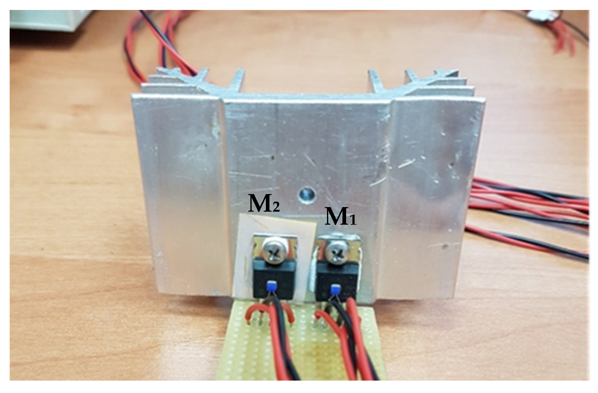
To verify the practical usefulness of the presented methods, the measurements of self and mutual thermal transient impedances for two power MOSFETs that were mounted on a heat-sink were carried out in the manner as shown in
Figure 1. The measurements were made using the methods and the measurement systems that are described in
Section 3 at different values of the power that was dissipated in transistor M
1. In the case of the electrical method, three thermo-sensitive parameters as well as the linear and quadratic approximations of thermometric characteristics were used. Some of the measurements that were made with the electrical method were repeated with the use of the contact and optical methods.
Figure 11a shows the dependence of thermal resistance of the transistor M
1 on the power that was measured with the use of different thermo-sensitive parameters as well as the linear and the quadratic approximations of thermometric characteristics.
Figure 11b shows the dependence of mutual thermal resistance between transistors M
1 and M
2 on the power that was dissipated in transistor M
1. The measurements were performed using the electrical, optical, and contact methods. The solid lines mark the results that were obtained using the square approximation of the thermometric characteristic and the dashed lines mark the results that were obtained using the linear approximation of this characteristic.
As shown in
Figure 11a, the measured dependences R
th(p) are non-linear and the differences in the results that were obtained using the square and linear approximations of thermometric characteristics and different thermo-sensitive parameters decrease with the increasing power. The measured values of thermal resistance of the investigated device also decreased with an increase of the power that was dissipated in the transistor, with the exception of the characteristic that was obtained using voltage v
DS as a TSP and the linear approximation of the thermometric characteristic. In this case, the dependence R
th(p) had a local minimum, which had no physical justification. The differences in the thermal resistance that were obtained with the use of the linear and non-linear approximations of thermometric characteristics for this thermo-sensitive parameter were the biggest and reached 24% at the power p = 5 W.
At the same value of power, smaller differences in the value Rth were obtained by using voltage vGS as a thermo-sensitive parameter. In this case, the thermal resistance values that were determined on the basis of the linear and quadratic approximations of thermometric characteristics did not differ from each other by more than 10%. In the case of voltage vF, the maximum difference in the value Rth was less than 2%.
The thermal resistance values that were obtained using v
GS and v
F voltages and the square approximation of thermometric characteristics differed by less than 5% over the entire power range under consideration. It should be noted that for p > 20 W, the results that were obtained using v
F, v
GS, and the linear and quadratic approximations, as well as the results that were obtained using v
DS and the linear approximation differed by about 4% at 20 W and by 3.3% at the power of 24 W. Despite the use of the quadratic approximation of the thermometric characteristic, in the case of voltage v
DS the result was higher by the approximation of high values of the power p, e.g., at 24 W, and may be associated with the difficulty in providing constant cooling conditions in a situation where the main mechanism of the device cooling is natural convection. In such a situation, even a slight movement of the air around the heat sink can significantly affect the internal temperature of the investigated transistors [
40]. The use of the linear approximation of thermometric characteristics caused a decrease in the thermal resistance value by up to 20%.
The measured values of mutual thermal resistance Rth21 were lower than the corresponding values of thermal resistance Rth. For all of the measurement methods, a monotonically decreasing dependence of Rth21(p) was obtained. The values of Rth21 and Rth that were obtained with the optical and contact methods were, in all the cases, less than the corresponding values of these parameters that were measured with the electrical method. The differences between these values were up to 50% in the case of Rth and 35% in the case of Rth21.
An important problem is not only the reliable measurement of the thermal resistance value, but also the measurements of the transient thermal impedance waveforms. This problem is important because the values of thermal time constants are determined using the transient thermal impedance waveforms [
11] and are used as parameters of thermal models that allow, e.g., for determination of the internal temperature waveforms of the tested devices.
Figure 12 compares the waveforms of transient thermal impedance of transistor M
1 that was measured in the setup shown in
Figure 3, using the linear (
Figure 12a) and the quadratic (
Figure 12b) approximations of its thermometric characteristics T
j(v
GS). The presented results were obtained for different values of power that were dissipated in this transistor.
As can be seen, the waveforms of transient thermal impedance of transistor M
1 that were obtained using the linear and quadratic approximation of thermometric characteristics and voltage v
GS as a thermo-sensitive parameter differed significantly from each other. For the time t = 10 s, the differences reached as much as 15%. The linear approximation of the non-linear thermometric characteristic caused a distortion of the transient thermal impedance waveforms, including the overestimation or underestimation of the thermal resistance value.
Figure 12a shows the non-physical observation that the thermal resistance that was obtained at p = 20 W was lower than that obtained at p = 24 W, and from
Figure 12b it can be seen that the opposite relation is true.
The use of the cooling curve in the measurements of
Zth(
t) caused a reversal of the trend resulting from
Figure 8 and
Figure 9, consisting in lowering the value of the internal temperature and the difference
Tj −
Ta using the linear approximation of the dependence T
j(TSP). In the case of measuring the waveform
Zth(
t), the value of this parameter was underestimated at the extremes of the temperature interval that was considered in
Figure 8 and overestimated in the central part of this interval.
In turn,
Figure 13 shows the transient thermal impedance waveforms that were obtained using voltage v
DS and the approximation of the thermometric characteristic by a square function.
As can be seen,
Zth(
t) waveforms that were obtained for different power values in the interval
t < 200 s overlap. This transient thermal impedance pattern is associated with the removal of heat from the die of transistor M
1 by the heat conductivity mechanism. The
Zth(
t) waveforms in the time interval
t > 200 s for different values of the power that was dissipated in the transistor M
1 are related to an increase in the efficiency of natural convection with an increase of the temperature of the heat-sink, on which both the transistors are mounted [
40]. With an increase in the power in the range from 5 to 24.6 W, the value of thermal resistance decreased by over 20%.
Figure 14 shows the waveforms of mutual thermal impedance Z
th21(t) between the transistors at selected values of the power that was dissipated in transistor M
1.
The recording of Zth21(t) waveforms allows for the analysis of delays in the heat flow in the tested system. As it is visible, the waveform starts after about 1 s from switching on the power dissipated in transistor M1. This is the time that is necessary for thermal energy to travel from the die of transistor M1 to the die of transistor M2. An increase in the power that is dissipated in transistor M1 in the range from 5 to 24 W causes a decrease in the value of the parameter under consideration at the steady state even by 35%.
Figure 15 compares the waveforms of the internal temperature and the case temperature of the transistors M
1 and M
2 that were measured during the power dissipation with a step shape of 24 W in transistor M
1. The internal temperature was measured by the electrical method and the case temperature was measured by the contact method.
As expected, the internal temperature of transistor M1 increased the fastest and reached its highest value in the steady state. There is a visible delay in the course of other temperatures by a few seconds in relation to the course of Tj1(t). It is worth noting that the heat transfer between the semiconductor dies of both the transistors through the common heat-sink is more effective than the heat transfer between the semiconductor die and the case of transistor M1. In the steady state, the differences between the temperatures under consideration exceeded even 50 °C.
Figure 16 compares the excess over the ambient temperature in:
- (a)
the internal temperature Tj of the transistors M1 and M2 in the steady state that were obtained using the electrical method,
- (b)
the case temperature Tc that was obtained by the contact method,
- (c)
the temperature of the heat-sink Tra that was obtained by the optical method.
The measurements were made with the power dissipated in the transistor that was equal to 20 W. Index 1 is the symbols of particular temperatures that relate to transistor M1, and index 2 relates to transistor M2.
The values of temperatures T
j2, T
c1, T
c2, T
ra1, and T
ra2 that are presented in the
Figure 16 are the result of averaging from three results of the measurements that were performed with the use of each thermo-sensitive parameter.
As can be seen, the dissipation of the power of 20 W in transistor M1 caused its internal temperature to rise above the ambient temperature by about 100 °C. The results that were obtained with the electrical method using voltages vGS and vF as a TSP differ from each other by only 2 °C. The temperature obtained by using voltage vDS as a TSP is 13 °C higher. Both the temperature of the heat-sink and the temperature of the case of transistor M1 were lower than the internal temperature that was measured by the electrical method. The temperature of the heat-sink was lower by 20 °C and the case temperature of transistor M1 by 27.5 °C. As can be seen, the use of the case temperature or the heat-sink temperature to determine the thermal resistance can lead to the values Rth lowered by 20% or 27.5%, respectively.
In turn, the internal temperature of transistor M2 increased above the ambient temperature only due to thermal coupling with transistor M1 by as much as 81.5 °C. As can be seen, thermal coupling can cause a significant increase in the internal temperature of the coupled device solely due to the flow of heat from the device in which the power is dissipated. This increase in temperature, due to thermal coupling, should be taken into account in the design process as it may be important in the case of, e.g., the cyclical operation of one of the components. The described phenomenon is also important from the point of view of stabilising the internal temperature of semiconductor devices. Mounting the devices to a common heat-sink and their thermal coupling can reduce temperature variations during thermal cycling and consequently improve the system reliability. Thermal cycles consist of rapid heating of the semi-conductive structure to high temperatures as a result of a cyclic release of the significant power in the device and rapid cooling of this structure after the power is turned off. On the other hand, the omission of thermal couplings between the elements when designing the cooling system may result in a failure of one of the elements as a result of exceeding the allowable internal temperature.
Mutual thermal resistance Rth21 that was determined using the electrical method is 4 K/W. The heat-sink temperature Tra2 that was obtained from the measurement with the optical method was lower by 3 °C than Tj2. Taking into account the heat flow in the tested system, such a result has no physical justification and is probably related to the measurement errors. In turn, the temperature of transistor M2 case was lower than its internal temperature by 16 °C.
In the case when the measured temperature value Tc2 is used to determine the thermal resistance Rth21, the result will be lower by 20%, and in the case when temperature Tra2 is used–only by 3.5%.
Thermal parameters of the investigated transistors depend not only on the dissipated power, but also on the cooling conditions. In
Figure 17 the dependences of thermal resistance and transfer thermal impedance on air flow speed v are presented. The measurements were performed at the power that was dissipated in transistor M
1 equal to 20 W.
As it is visible, the transfer thermal resistance was smaller by about 1 K/W than thermal resistance of transistor M1. Both the dependences Rth(v) and Rth12(v) are monotonically decreasing functions. In the considered range of the change in the air flow speed, the values of thermal parameters decreased even by 70%. This decrease results from an increase in the efficiency of heat convection on the surface of the heat-sink.
7. Conclusions
The paper presents the results of investigations of selected methods of measuring thermal parameters of power MOSFETs. The manner of implementation of the contact, optical, and electrical methods of measuring these parameters is presented. The measurement error of the considered methods was analyzed and the selected results of the measurements that were carried out with the use of these methods are presented.
The performed investigations show that the electrical methods ensure obtaining higher values of the internal temperature of the power MOSFETs during its operation than the contact and optical methods. The difference in the measured values of the transistor internal temperature increase above the ambient temperature with the use of the considered methods may exceed 20%.
While determining waveforms Zth(t), the use of the contact methods result in obtaining the waveforms that are lowered and delayed in relation to the results that were obtained with the electrical method. It was shown that, in the case of the electrical methods, the accuracy of the approximation of the thermometric characteristic has a large influence on the measurement error. If the voltage across a body diode is used as a thermo-sensitive parameter, the linear approximation of this characteristic gives satisfactory results. On the other hand, when voltages vDS or vGS are used as a TSP, satisfactory accuracy is ensured by the approximation of the thermometric characteristic by a quadratic function. For each of the considered measurement methods, the measurement error of thermal resistance is a decreasing function of the power that is dissipated in the transistor. The best accuracy of the measurements is obtained for voltage vGS used as a TSP and the quadratic function approximating the thermometric characteristic.
The obtained Zth(t) waveforms prove that the selection of the function approximating the thermometric characteristic may have an impact on the credibility of the results that were obtained with the use of electrical methods. For example, it is possible to obtain a false measurement result, indicating an influence of the power dissipated in the transistor on Zth(t) waveform in a range of low values of time, where only heat conduction is responsible for the heat transfer.
The performed analysis of the accuracy of the considered measurement methods makes it possible to select the most accurate method. With this method, the accurate value of the device’s internal temperature can be estimated. This temperature determines the lifetime of the network containing this device.
When measuring thermal parameters of power MOSFETs that are situated on a common heat-sink, it was shown that the heat transfer between these transistors occurs mainly due to heat conduction through the heat-sink. This transfer is more effective than between the semiconductor die of the transistor and its case. Therefore, the use of the contact and optical methods causes a significant underestimation of the measured values of thermal parameters. This is an obvious theorem when measuring the transistor’s self thermal parameters. However, the presented investigation results also showed that the mutual thermal parameters that were measured using these methods are also underestimated. A very important consideration for the designer of power electronics networks is presented in
Figure 16, which shows that the use of the contact methods to measure the device internal temperature can cause a big error that exceeded even 50 °C; much better accuracy can be obtained using the electrical methods.
The results of the investigation present only one type of power MOSFETs with the case TO-220. The conclusions of the performed measurements have global applicability. The presented discussion about the measurement methods is universal for all power MOSFETs. The analysis of the measurement error gives the same results for different types of considered devices. On the other hand, the results of the measurements will be similar for different semiconductor devices (MOSFETs, BJTs, IGBTs, diodes) that are mounted in TO-220 cases. The differences between the results that were obtained with the use of the electrical, optical, and contact methods will be similar for different semiconductor devices that are mounted in such cases.
The results of the investigation that are presented in this paper may be useful for designers of power semiconductor devices and networks with these devices, and for designers of setups for measuring the thermal parameters of these devices. They can be also applied in many communications systems that are used in the internet of things or autonomous vehicles that are considered in [
41,
42].
The investigations that are presented in this article can be continued to examine an influence of the different shape and thickness of heat-sinks on the thermal parameters of semiconductor devices. An influence of temperature and forced cooling conditions on these parameters can be also investigated.


