Article

AC Current Ripple in Three-Phase Four-Leg PWM Converters with Neutral Line Inductor

Department of Electrical, Electronic, and Information Engineering, University of Bologna, 40136 Bologna, Italy
*
Author to whom correspondence should be addressed.
Energies 2021, 14(5), 1430; https://doi.org/10.3390/en14051430
Submission received: 7 February 2021 / Revised: 26 February 2021 / Accepted: 2 March 2021 / Published: 5 March 2021
(This article belongs to the Section F: Electrical Engineering)

Abstract

:
This paper presents a comprehensive study of peak-to-peak and root-mean-square (RMS) values of AC current ripples with balanced and unbalanced fundamental currents in a generic case of three-phase four-leg converters with uncoupled AC interface inductors present in all three phases and in neutral. The AC current ripple characteristics were determined for both phase and neutral currents, considering the sinusoidal pulse-width modulation (SPWM) method. The derived expressions are simple, effective, and ready for accurate AC current ripple calculations in three- or four-leg converters. This is particularly handy in the converter design process, since there is no need for heavy numerical simulations to determine an optimal set of design parameters, such as switching frequency and line inductances, based on the grid code or load restrictions in terms of AC current ripple. Particular attention has been paid to the performance comparison between the conventional three-phase three-leg converter and its four-leg counterpart, with distinct line inductance values in the neutral wire. In addition to that, a design example was performed to demonstrate the power of the derived equations. Numerical simulations and extensive experimental tests were thoroughly verified the analytical developments.

Graphical Abstract

1. Introduction

Three-phase converters have been extensively employed as an interface between AC distribution networks and the distributed energy sources, such as photovoltaic and wind farms, DC microgrids, and energy storage systems [1]. Another popular tendency in the automotive industry is to apply three-phase converters as a power factor correction stage in on- or off-board electrical vehicle (EV) battery chargers [2,3]. When there is a necessity to supply unbalanced loads (e.g., single-phase loads in the three-phase systems) or to be linked with weak unbalanced grids, three-phase four-wire converters are usually adopted to provide an additional path for the zero-sequence current [4]. A recent example of such technology is power conditioning services in smart grids utilizing EV energy storage, known as vehicle-to-grid (V2G), vehicle-to-home (V2H), or general term vehicle-to-everything (V2X) [5,6]. There are various three-phase four-wire topologies available in the literature/market, but only three are widely applied: split-capacitor [7,8], four-leg [6,9], and independently controlled neutral module [10,11]. These voltage source converters (VSCs) can either have or not have the fourth wire’s neutral line inductor.
The converter topology’s modulation methods are classified into two categories: carrier-based pulse-width modulation (CBPWM) or space vector modulation (SVM). The 3D SVM method for four-leg converters was comprehensively described in [12]. However, the implementation is complex and computationally heavy to determine sector location and turn-on times for switching devices [4]. Therefore, it requires powerful and expensive controllers. On the other hand, the family of CBPWM schemes guarantees a simple implementation in both analog and digital systems, a fixed switching frequency, and a well-defined harmonic spectrum [13,14]. Among the different CBPMW methods, only two are commonly applied, namely sinusoidal pulse-width modulation (SPWM) and centered pulse-width modulation (CPWM). The latter is the carrier-based analog of SVM [15].
This paper is dedicated to AC current ripple analysis in four-leg converters with the neutral line inductor. The inductance value of the neutral line inductor has a variable form. Thus, the current study covers a broad range of four-leg converter designs. The SPWM scheme was selected for this paper, while the other modulation methods were beyond the analysis scope and will be examined in further publications.
An AC current ripple study is essential for converter designs to size the reactive interface components (filters), to select an optimal switching frequency, to perform switching losses and efficiency calculations, and to eventually adopt an optimized modulation strategy [16]. An extensive peak-to-peak AC current ripple analysis for three-phase, three-leg converters based on current ripple envelope prediction is given in [17]. The importance of current ripple envelopes was reported in [18]. Knowledge of AC current ripple spreading over the fundamental period is crucial for multiple zero-crossing intervals computation. An accurate assessment of these intervals is necessary to properly compensate for the lost volt-seconds due to dead-times, especially for high ripple currents [19]. In [7], the authors reported the phase’s optimized design and neutral line inductors in three-phase split-capacitor converters. The analysis focused only on the peak-to-peak AC current ripple prediction and did not estimate the current total harmonic distortion (THD) caused by the converter’s operation.
Furthermore, the presented study for the peak-to-peak value of the phase current ripple is limited to a few inductance values of the neutral line inductor, missing the part that explains the current ripple behavior for other possible inductance values of a neutral line inductor. In addition to that, the neutral current ripple has not been investigated at all. Reference [20] instead provided a thorough analysis of AC current ripples for three-phase split-capacitor VSCs without a neutral line inductor. In [21], the authors were unsuccessful in finding an explicit form of the maximum peak-to-peak value of the phase current ripple in the four-leg VSC with a neutral line inductor. Instead, they introduced an approximated fitting method. Furthermore, the whole current ripple examination was based on a three-phase balanced operation; therefore, the maximum peak-to-peak value of a phase current ripple under unbalanced current conditions was estimated by a random choice of fitting coefficients. In addition to that, neither investigations on the maximum peak-to-peak value of the current ripple in the neutral wire nor derivation of the root-mean-square RMS value of the current ripple for both phase and neutral have been given. The authors in [22] compared different value combinations of phase and neutral line inductors. However, their ultimate selection has not yet been analytically validated. On the other hand, the authors in [23] demonstrated that, in the four-leg converter with equal inductors in the phases and neutral, it is possible to obtain the smallest amplitude of the load neutral point voltage. Nevertheless, the paper was focused on mitigation of the load neutral point voltage in the four-leg converters while current ripple characteristics were not investigated.
Apart from finding envelopes that completely wrap the current ripple (primary envelope), as it was commonly accepted before, the authors in [24] proposed to take into account an intermediate ripple (secondary envelope) for general AC current ripple assessment. The significance of this secondary envelope was discussed and clearly illustrated. It has been demonstrated that this consideration permits us to obtain an accurate expression for the RMS value of a phase current switching ripple. Another significant work regarding this matter was conducted in [25]. Reference [25] focused on the three-phase four-leg VSC topology without a neutral inductor and reported the AC current ripple characteristics in the case of the most common discontinuous PWM strategies. Although some current-ripple-related characteristics concerning the most common continuous PWMs were introduced for the sake of comparison, they were not discussed in great detail. Moreover, as shown later, the equations derived in [25] of peak-to-peak and RMS values of AC current ripple are not applicable in the case of three-phase, four-leg VSCs with a neutral line inductor.
To the best of the author’s knowledge, no publications so far have provided a complete AC phase and neutral current ripple analysis, computing both maximum peak-to-peak and RMS values for general-shape three-phase, four-leg VSCs with an inductor placed in the fourth (neutral) wire and working under balanced and unbalanced fundamental currents. Prior to this study, neither maximum peak-to-peak nor RMS values of an AC current ripple have been analytically derived in a well-defined, precise, generic form considering optimal sizing of the neutral line inductor. This was achieved by introducing a quantitative relation of the neutral line inductance for the phase analogy (“k factor”) into the analysis. By setting this k factor to any of two extrema, namely zero or positive infinity, the described topology becomes either a three-phase, four-leg VSC without a neutral inductor or a conventional three-phase, three-leg VSC. As a result, current ripple envelopes (peak values) were determined in the fundamental period as functions of the fundamental angle, modulation index, and the k factor. Knowing the AC current ripple distribution in one fundamental period, other ripple properties, such as maximum peak-to-peak and true RMS expressions, were derived as the modulation index functions and the k factor for both phase and neutral current ripples. The obtained expressions are especially convenient for the converter design process, producing accurate results without running computationally heavy repetitive numerical simulations. For example, by defining input design parameters, such as DC voltage level, switching frequency, and restricted current ripple characteristics (maximum peak-to-peak or/and RMS values), it is almost straightforward to optimally size the interfacing AC inductors, including that in the neutral wire. Another practical scenario is that, by knowing the design parameters of a specific four-leg power converter, one can quickly compute the total harmonic distortion (THD) or total demand distortion (TDD) given by the converter functioning at any certain operating point and can check compliance with the associated standard.
Another contribution given by this work is a comprehensive examination of the AC current ripple characteristics between four-leg converters with several assemblies of the neutral line inductor and their conventional three-leg counterpart. Specifically, the comparison is realized by equalizing one metric per time relating the effect to the others. This procedure helps us define a range with optimal neutral line inductance or to estimate a reduction in switching frequency/line inductance value, fixing one of the current ripple characteristics with respect to the other possible converter designs. All the analytical expressions were broadly validated through both numerical simulations and laboratory tests. The achieved results demonstrate an adequate match with the theoretical derivations.
The paper is organized as follows. Section 2 provides a basic description of the converter circuit, the assumptions considered during the current analysis, and some background on the SPWM method. A study of the phase current ripple and the evaluation of its maximum peak-to-peak and RMS values are presented in Section 3. A similar investigation for the neutral current ripple is introduced in Section 4. The following Section 5 discusses the current-ripple-related performances of the compared structures and provides an optimal design example of the front-end power factor correction (PFC) converter of an on-board electrical vehicle charger based on the three-phase, four-leg architecture with a neutral line inductor. Experimental validation is presented in Section 6. Section 7 summarizes the key outcomes of this paper and concludes the discussion.

2. Basic Assumptions and Modulation Principle

2.1. Converter Model and Current Ripple Definition

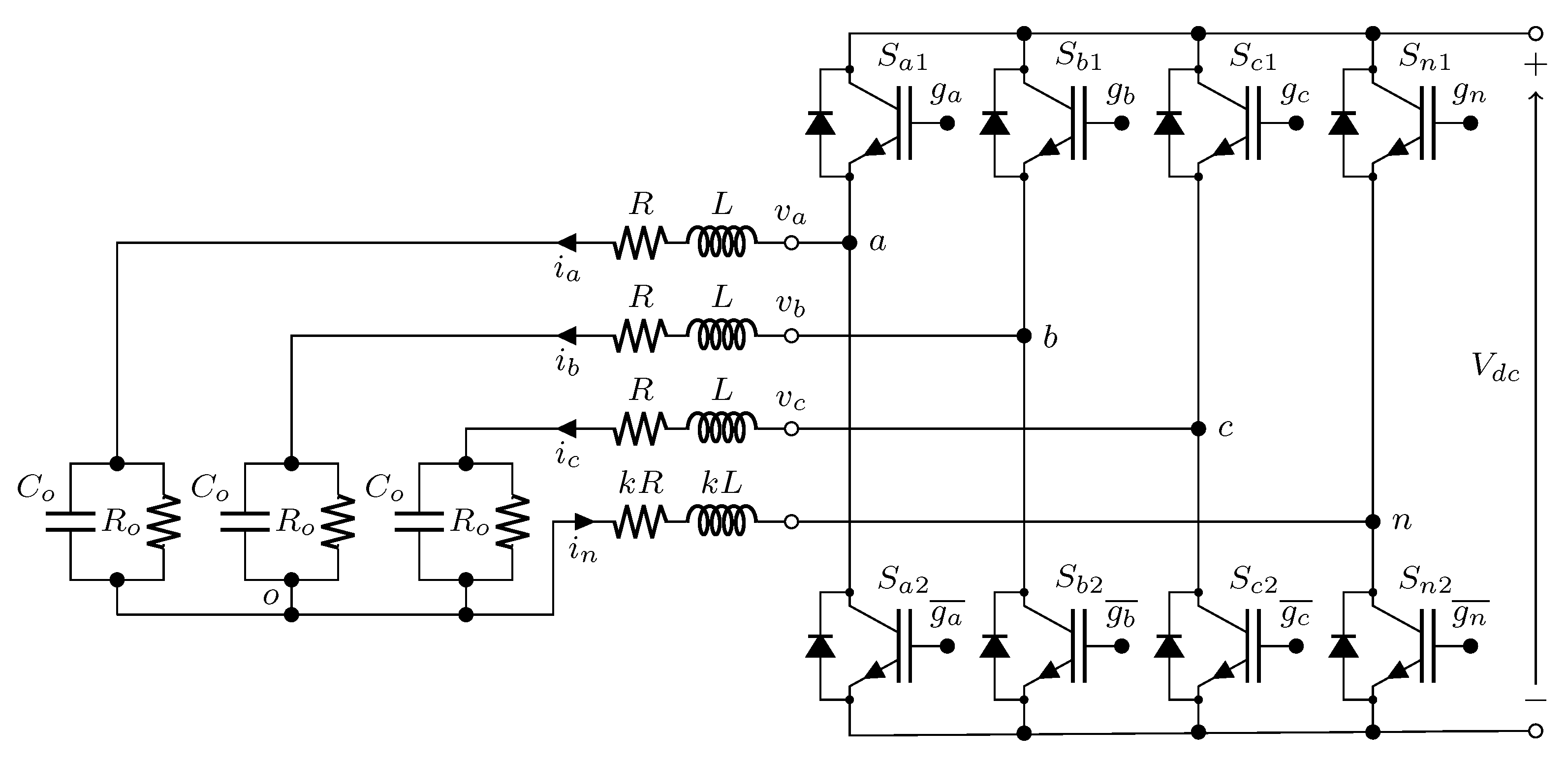
The converter was built out of four identical legs, where each of them was made up of two power electronic switches, as illustrated in Figure 1. The four-leg VSC was supplied by a DC source with constant voltage (Vdc) and linked with grid/load through magnetically independent interface inductors. These inductors were present in each phase (L) and the neutral link (kL). Therefore, the middle point (n) of the fourth leg was tied to the neutral point (o) of the grid/load through an inductor. The coefficient k, designated as the “k factor”, represents a ratio between the inductance placed in the neutral link and phase inductance. This k parameter can be virtually any positive number starting from zero to infinity. Zero value represents the specific case of four-leg topology without the neutral line inductor [24,25], whereas infinity is equivalent to a three-phase, three-leg topology [17]. Nevertheless, in the four-leg topology practical applications, it is unlikely to use an inductor in the neutral connection with an inductance value higher than a few times the phase one. Therefore, most of the presented results, given below, were prepared for just a few relevant cases. Here, an additional comment must be left. The grid/load equivalent inductance also has an additive effect on AC current ripple characteristics. To compute an optimal inductance value of the neutral inductor, this fact must be taken into consideration. However, for the sake of simplicity and generality, the equivalent phase inductance of the system “grid/load-converter” is not decomposed into two terms and is labeled here as “L”.
This paper aims to report an AC current ripple analysis mainly for grid-tied applications; therefore, the current examination was limited to unity power factor circuits only. Nonetheless, for the sake of clarity, it must be noted that the AC current ripple characteristics are independent of the phase angle φ (determines power factor). In such a way, all the expressions presented below are equally valid for the circutis with any abstract power factor. With reference to grid-connected applications, this study assumes the grid voltages to be balanced. Since the AC coupling reactance (typically 0.05–0.08 p.u.) is small, considerably large unbalanced currents can be obtained by a slight asymmetry between converter voltages (in the order of a few percent). Therefore, the three corresponding modulating signals at any operating point can be considered quasi-balanced, employing a unique modulation index. That also means that the switching current ripple is independent of the direction of power flow. Thus, the derived equations are correct for the four-leg inverter supplying an unbalanced load.
The literature given in the Introduction discusses all related definitions of AC switching current ripple in great detail. For example, the authors in [24,25] described the mathematical background very clearly. Therefore, for the sake of conciseness, here, only a brief overview is given. With regard to Figure 1 and independent from the direction of power flow, the basic mathematical definition of the four-leg VSC with the neutral line inductor can be written as follows:
v x t = R i x t + L d i x t d t + e x t + R n i n t + k L d i n t d t
Kirchhoff’s current law is as follows:
i a t + i b t + i c t = i n t
where subscript x denotes the corresponding phase index (a, b, c); vx represents converter terminal voltage, which is the resultant voltage between the phase-leg midpoint (a, b, c) and the neutral midpoint (n); ix and in are the instantaneous phase and neutral currents, respectively; ex denotes the grid/load (in Figure 1, illustrated as a dashed box) phase voltage; R and Rn (not depicted) represent internal resistance of the interface phase and neutral inductors, respectively. The voltage vx and currents ix and in can be presented in terms of harmonic components as follows:
v x t = v ¯ x t + v ^ x t i x t = i ¯ x t + i ^ x t   i n t = i ¯ n t + i ^ n t  
where v ¯ x , i ¯ x , and i ¯ n are the fundamental (or low-frequency) components (i.e., averaged over the switching period Tsw) and v ^ x , i ^ x and i ^ n are the switching (high-frequency) ripple components. The voltage ex(t) is eventually almost sinusoidal, without contributions from the high-frequency components; thus, Equation (1) can be decomposed based on the low- and high-frequency ripple components, leading to a formulation of switching counterparts:
v ^ x t = R i ^ x t + L d i ^ x t d t + R n i ^ n t + k L d i ^ n t d t
Since the resistive voltage drop due to current ripple i ^ x or i ^ n is negligible in comparison to the voltage ripple component v ^ x (having an amplitude in the order of Vdc) and bearing in mind Equation (2), Equation (4) can be simplified and rewritten for each converter terminal voltage as follows:
v ^ a t v ^ b t v ^ c t L d d t k + 1 i ^ a t + k i ^ b t + k i ^ c t k i ^ a t + k + 1 i ^ b t + k i ^ c t k i ^ a t + k i ^ b t + k + 1 i ^ c t
Based on Equation (5), the instantaneous phase voltage can be expressed then as follows:
v ^ a o t v ^ b o t v ^ c o t v ^ o n t L d d t i ^ a t i ^ b t i ^ c t k i ^ n t = 1 3 k + 1 2 k + 1 v ^ a t k v ^ b t k v ^ c t k v ^ a t + 2 k + 1 v ^ b t k v ^ c t k v ^ a t k v ^ b t + 2 k + 1 v ^ c t k v ^ a t + v ^ b t + v ^ c t
Finally, an integration of the right-hand side of Equation (6) leads to a mathematical definition of the instantaneous current ripple:
i ^ a t i ^ b t i ^ c t i ^ n t i ^ a 0 i ^ b 0 i ^ c 0 i ^ n 0 + 1 3 k + 1 L 0 t 2 k + 1 v ^ a t k v ^ b t k v ^ c t k v ^ a t + 2 k + 1 v ^ b t k v ^ c t k v ^ a t k v ^ b t + 2 k + 1 v ^ c t v ^ a t + v ^ b t + v ^ c t d t
The converter terminal voltage vx, which is the voltage between output terminal x and the midpoint of 4th leg n, is expressed as follows:
v x t = V d c g x t g n t
where gx and gn are gate signals of the upper switches in phase leg x and neutral leg n, respectively. One can notice from Equation (8) that the three inverter voltages are dependent on the gate signals of the corresponding phase and neutral legs only. Therefore, these voltages can be treated as independent from each other.
The three-phase reference voltages (fundamental components) are given by the following:
v ¯ x t = 2 V ¯ x cos ϑ x = V d c m x cos ϑ x
where V ¯ x represents the RMS of the fundamental component of phase voltage and ϑx is the fundamental angle. For the balanced case, V ¯ a = V ¯ b = V ¯ c = V ¯ , ϑa = ωt, ϑb = ωt –2π/3, ϑc = ωt + 2π/3, with ω being the fundamental (grid) angular frequency. Modulation index mx is defined here as the ratio between the amplitude of the fundamental voltage component ( 2 V ¯ x ) and the DC-link voltage (Vdc). In the case of balanced sinusoidal modulation, ma = mb = mc = m. The linear modulation range is m = [0, 0.5]. As highlighted earlier, in most grid-connected applications, the unbalanced currents can be driven even by small modulation index unbalances (in the order of a few percent). Therefore, it is acceptable to assume that ma mb mc = m while the AC currents are unbalanced. As shown further, this assumption does not introduce critical effects on the validity of the findings.
The corresponding converter terminal voltage switching ripple component can be computed by inserting Equations (8) and (9) into Equation (3). Based on the obtained formula and Equation (7), the resultant expressions of the AC current ripple can be derived.
As illustrated in the following subsection, the amplitude of the peak-to-peak current ripple can be defined as follows:
i ^ x , p p t = max i ^ x t | T s w min i ^ x t | T s w

2.2. Carrie-Based Sinusoidal Pulse-Width Modulation (SPWM)

The SPWM technique that is employed in this article was implemented through a carrier-based approach. The generation of PWM gate signals is obtained by employing the classical comparison between modulating signals ux and triangular carrier signal cr. The modulating signals can be defined based on the phase reference voltages as follows:
u x t = v ¯ x t V d c = m x cos ϑ x u n t = 0                                
As visible, SPWM forces the neutral leg modulating signal un to be always zero.
Following what is stated in Equation (7), it is evident that the current ripple strongly depends on the voltage level and the voltage pulses disposition (visible inside the integrals). It can be demonstrated that the relative position determines the magnitude and pulse locations among each other for the reference voltages, which drive the gate signals of Equation (8). As it will be clear later, thanks to its quarter-wave symmetry, the current ripple description can be limited to the interval 0 ≤ ϑ ≤ π/2, employing three sectors defined as follows:
Sec tor   I t 0 = T s w 2 1 2 u a m , ϑ             t 1 = T s w 2 u a m , ϑ                         t 2 = T s w 2 u b m , ϑ                     t 3 = T s w 2 u b m , ϑ u c m , ϑ t 4 = T s w 2 1 2 + u c m , ϑ             for   0 ϑ π 6
Sec tor   II t 0 = T s w 2 1 2 u a m , ϑ             t 1 = T s w 2 u a m , ϑ u b m , ϑ t 2 = T s w 2 u b m , ϑ                         t 3 = T s w 2 u c m , ϑ                     t 4 = T s w 2 1 2 + u c m , ϑ             for   π 6 ϑ π 3
Sec tor   III t 0 = T s w 2 1 2 u b m , ϑ             t 1 = T s w 2 u b m , ϑ u a m , ϑ t 2 = T s w 2 u b m , ϑ                         t 3 = T s w 2 u c m , ϑ                     t 4 = T s w 2 1 2 + u c m , ϑ             for   π 3 ϑ π 2
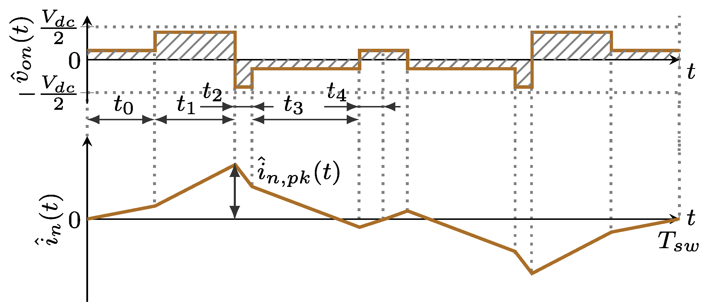
For the sake of clarity, Figure 2 depicts Sector I (0 ≤ ϑ ≤ π/6) of the voltage pulse disposition with reference to phase a. This figure presents a general case in one arbitrary switching period with the k factor equal to 1. Generalization with other possible values of k is omitted here for simplicity.

3. Analysis of Phase Currents Ripple

3.1. Phase Current Ripple Waveform

With reference to Figure 2, peaks (extrema) in the current switching ripple can be defined as the current ripple at the time instances when the derivative of the corresponding phase voltage ripple component changes its sign. That happens any time when this voltage ripple component crosses the zero level. In general, case peaks of the phase current ripple can be expressed by the following:
i ^ x , p k m , ϑ , k = V d c 2 L f s w r ^ x , p k m , ϑ , k   i ^ x , p k m , ϑ , k = V d c 2 L f s w r ^ x , p k m , ϑ , k
where î’x,pk and î”x,pk are primary and secondary current ripple envelopes, respectively; r ^ x , p k and r ^ x , p k are the corresponding normalized primary and secondary envelope functions; and Vdc/(2Lfsw) is a normalization factor. The current ripple envelopes enclose peak values of the global (primary) and local (secondary) maxima of the current ripple [24,25]. Strictly speaking, this definition is valid for k = 0 only, while for other possible values of k, these envelopes interchange between themselves depending on the value assumed by ϑ. However, for the sake of comparison and simplicity, this definition is preserved in this paper. It also must be emphasized here that both primary and secondary peaks compose the total current ripple. The researchers usually omit the smaller one since it does not contribute to the ripple’s maximum peak-to-peak value. Nevertheless, it plays a significant role in true RMS computation, as it will be shown in Section 3.2.
As it was pointed out in Section 2, the phase current ripple component, in its general form (as a function of k), has a complex structure and can only be defined as a piecewise function. The whole derivation process is quite laborious and bulky. However, it follows the idea that is well-described in [24,25]. Therefore, this part will be omitted here and only the final result will be presented.
The primary normalized current ripple envelope over the fundamental period can be written as follows:
r ^ x , p k m , ϑ , k = ± { m k + 1 6 k + 2   cos ϑ if   17 m 2   cos ϑ 1 m cos ϑ + 3 m sin ϑ 3 m k sin ϑ 3 k + 1 if   18 m 6 k + 2   2 k + 1 cos ϑ 3 k sin ϑ if   19 m 2   cos ϑ 1 m cos ϑ 3 m sin ϑ otherwise
with the following conditions:
2 k 3 k + 1 m σ 7 σ 6 σ 2 σ 3 σ 7 σ 4 σ 2 σ 5 ϑ σ 1 ϑ π σ 1 k < 1
σ 2 σ 5 σ 2 σ 4 k σ 2 σ 3 σ 2 σ 6 k ϑ σ 1 ϑ π σ 1
ϑ σ 1 ϑ π σ 1
where
σ 1 σ 2 σ 3 σ 4 σ 5 σ 6 σ 7 = R cos 1 k m 3 k + 1 3 k   tan ϑ k m cos ϑ 4 π 3 6 k + 2 m cos ϑ 4 π 3 6 k + 2 k m cos ϑ + π 3 6 k + 2 m cos ϑ π 3 6 k + 2 k 3 tan   ϑ + 1
The secondary normalized current ripple envelope is represented by the following:
r ^ x , p k m , ϑ , k = ± m cos   ϑ 1 2 m cos   ϑ 2                         if   ϑ π 3 ϑ π π 3     m cos   ϑ + 3 k sin   ϑ 6 k + 2 m   cos   ϑ 2   if   ( ϑ ϑ π ) π 3 , 2 π 3
To represent the envelopes of the current ripple in the whole fundamental cycle [0, 2π], the absolute values of sine-like functions are taken into account in Equations (16) and (21). The sign of the whole right-hand side of these expressions indicates which envelope (positive or negative) is determined.
As it was demonstrated in [24], Equations (16) and (21) are equally valid for balanced and unbalanced modulations (e.g., modulation indices among phases are different) at k = 0 since, in this particular case, the phase voltages are independent from each other. Therefore, the corresponding three-phase four-leg converter can be considered three independent single-phase converters. On the other hand, for k > 0, the phase voltages can be defined as a linear combination of the converter’s terminal voltages (cf. Equation (6)). Therefore, any unbalance in modulation signals will result in the corresponding ununiform current ripple distribution over the fundamental period. These conditions are difficult to represent mathematically in a compact, practicable form. Simultaneously, focusing solely on grid-connected applications, as described above, we can consider the modulation indices among phases equal between each other in all balanced and most unbalanced current conditions. It is also evident from Equations (16) and (21) that the current envelope functions are independent from the direction of power flow. Therefore, the derived expressions’ applicability can be demonstrated by a system “four-leg inverter—load”, depicted in Figure 3, operating under balanced modulation. In fact, in this case, the closed-loop regulator dynamic can be eliminated, making the simulation tests straightforward and reliable. For test purposes (both numerical simulations and the experimental part), the internal resistances of the interface inductors were taken into account. Here, the neutral line inductor internal resistance (Rn) was taken proportionally to its inductance (kR) for more straightforward implementation in the experimental setup, as will be explained in the corresponding section. It will also be proven later that these resistances do not affect the accuracy of the above derived equations.
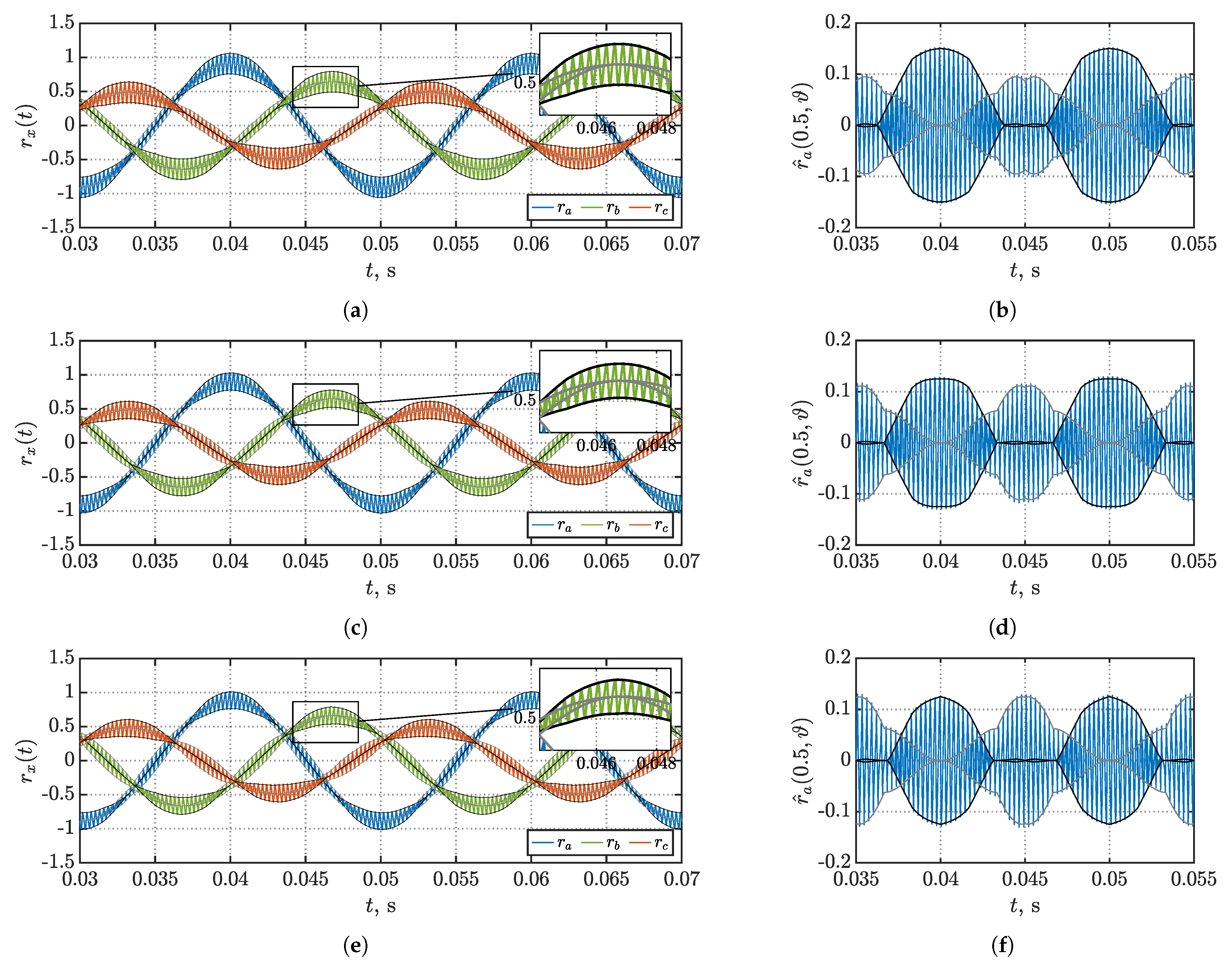
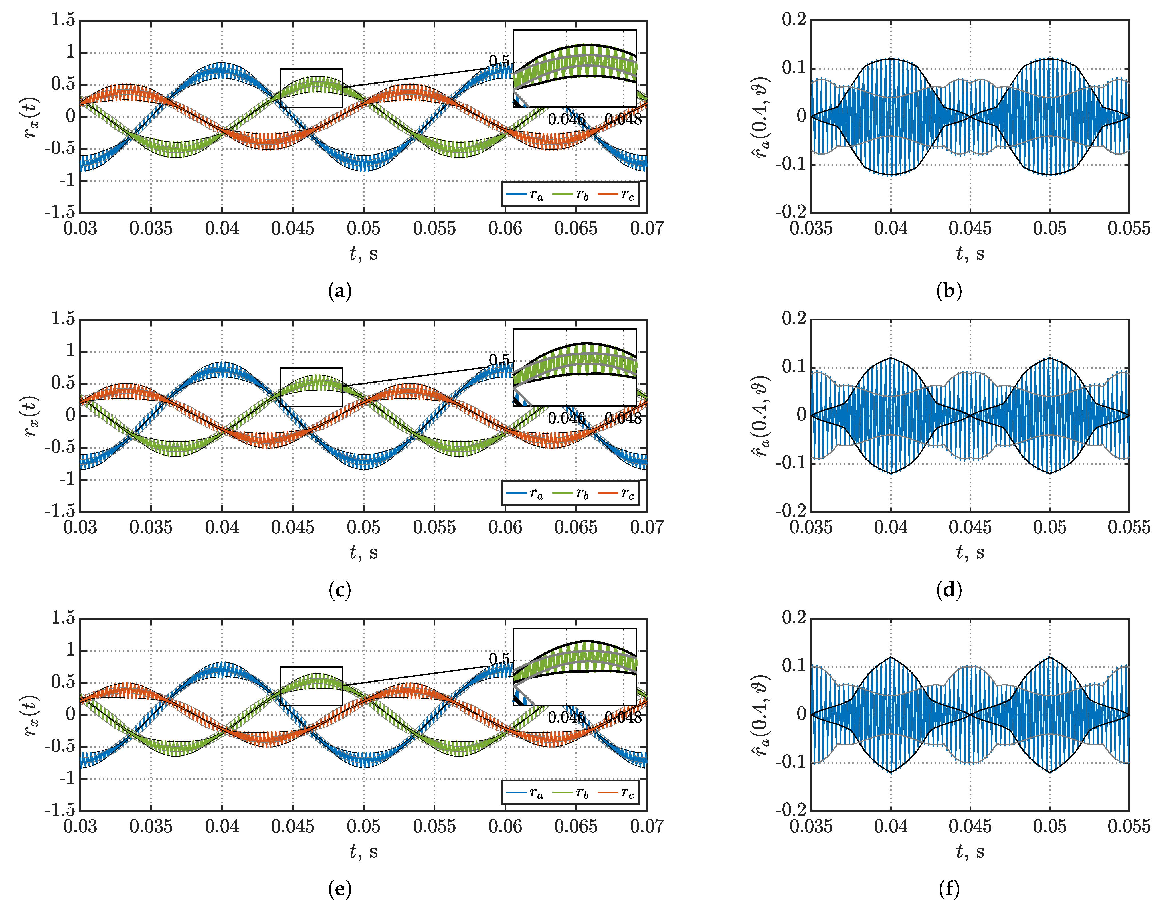
To verify the accuracy of Equations (16) and (21), the simulation results at different values of k factor and modulation index m are presented in Figure 4 and Figure 5. The subfigures marked with “(a)” demonstrate unbalanced three-phase currents wrapped by primary (black) and secondary (gray) envelopes. The normalized phase current ripple component (ph. a) is presented in the subfigures labeled by “(b)”. A relatively low switching frequency (fsw = 3.6 kHz) was chosen on purpose to clearly display the ripple profile with its primary and secondary envelopes. The main simulation parameters with reference to Figure 3 are summarized in Table 1. The load parameters were selected in such a way as to obtain a series resonance at the fundamental frequency. Therefore, the total dynamic impedance at the fundamental frequency is purely resistive (R + Ro) while AC capacitors (Co) maintain the voltage across the load resistors (Ro) imitating grid.
As shown in Figure 4 and Figure 5, envelopes of the current ripples nicely enclose the corresponding AC current ripples obtained by the simulations. It is also clear from the figures that the phase current ripple in four-leg converter configuration with a neutral line inductor is highly nonlinear and changes its shape depending on the fundamental angle and modulation index.
By introducing Equations (16) and (21) into (10) and by considering positive and negative sides of the ripple envelopes, the maximum profile of normalized peak-to-peak current ripples (primary and secondary) can be calculated as follows and depicted in Figure 6:
r ^ x , p p m , ϑ , k = 2   max r ^ x , p k m , ϑ , k , r ^ x , p k m , ϑ , k
Figure 6a–f illustrate the maximum normalized peak-to-peak current ripple profiles over half of the fundamental period for several relevant values of the k factor. In particular, Figure 6a depicts case (k = 0), well-defined in [24]. Moving onto the next case (k = 0.5) displayed in Figure 6b, apart from drastic shape change, one can notice a substantial reduction in the maximum current ripple value by 40%. In the next two cases, namely k = 1 (cf. Figure 6c) and k = 2 (cf. Figure 6d), the current ripple’s maximum value is the same although the shape of the profile is different. The reason lies in the redistribution of the primary and secondary ripple envelopes within that limit. One may notice in Figure 6d (cf. also Figure 4f) that the peak values of the maximum peak-to-peak ripple profile at ϑ = 0 and ϑ = ±π/2 are equal between each other.
On the other hand, when k = ∞ (three-leg converter, cf. Figure 6e), this value at ϑ = ±π/2 is larger by 13.4% than its counterpart at ϑ = 0. The latter (at ϑ = 0) does not change for k ≥ 1 and always stays at the 0.25 p.u. level. As a result, it is evident that, by using a four-leg topology with a neutral line inductor (inductance value in the range 12L) over conventional three-leg configuration, the maximum peak-to-peak value of the phase current ripple can be reduced by 13.4%. Alternatively, as it will be shown later that the phase inductors can be diminished by 13.4% while still employing four-leg converter capabilities. Figure 6f depicts the distribution of the maximum peak-to-peak value of the phase current ripple over the k factor range [0, 10]. The rise of the phase current ripple’s maximum peak-to-peak value with k > 2 is visible from this plot. As shown above, to derive an analytical formulation for the discussed maximum peak-to-peak function is very complex and unpractical. Therefore, Figure 6g presents a contour plot with numerical values of that function at certain modulation index m and k factor. The intermediate values of maximum peak-to-peak phase current ripple can be linearly interpolated within a given range. Figure 7 demonstrates the analyzed cases (cf. Figure 6) more comparatively and confirms the statements given above.

3.2. Phase Current Ripple RMS

Due to current ripple symmetry, it is possible to restrict the study to one-half of the switching period Tsw/2 (cf. Figure 2). For the current ripple as a periodic waveform composed of five piecewise segments in one half of the switching period, the exact RMS value is as follows:
I ^ x m , ϑ , k | T s w = 2 T s w j = 0 4 δ j t j
where δ j is the contribution of j segment and t j is the duration of that segment defined in Section 2.2. δ j depends on the shape of the segments. However, by looking at Figure 2, it is evident that each segment of the phase current ripple can be described as a trapezoidal waveform with the following:
δ j = 1 3 i ^ x 2 t j + i ^ x t j i ^ x t j + 1 + i ^ x 2 t j + 1
In Equation (24), the time point t 4 + 1 with reference to Figure 2 is the midpoint of the switching period. The time slots tj are expressed by Equations (12)–(14).
The total RMS value of phase current ripple can be obtained by integrating individual RMSs of each switching period over the fundamental period. However, as stated in Section 2.2, the definition of each time slot within a switching period depends on the modulating signals’ mutual position. Due to the quarter-wave symmetry of the fundamental component, the analysis can be performed only on one-quarter of the fundamental period. Eventually, there are three sectors to be considered, namely I—[0, π/6], II—[π/6, π/3], and III—[π/3, π/2].
I ^ x m , k = 2 π 0 π 6 I ^ x m , ϑ , k T s w I 2 d ϑ + π 6 π 3 I ^ x m , ϑ , k T s w II 2 d ϑ + π 3 π 2 I ^ x m , ϑ , k T s w III 2 d ϑ
Combining Equations (23)–(25) and introducing into the formula the time slots from Section 2.2 yield:
I ^ x m , k = V d c 2 L f s w   m x 2 6 1 16 3 π m 3 + 1 3 3 k + 1 2 + 3 m 2
Similar to (15), the normalization of (26) leads to the normalized RMS of the phase current:
R ^ x m , k = m 2 6 1 16 3 π m 3 + 1 3 3 k + 1 2 + 3 m 2
From Equation (27), it is straightforward to obtain the RMS current ripple expressions for the four-leg topology exceptional cases, namely when k = 0 and k = ∞. By setting k = 0, one may obtain the RMS expression given in [24]. On the other hand, by introducing k = ∞, it is possible to derive the exact RMS formula of the current ripple for the three-leg topology.
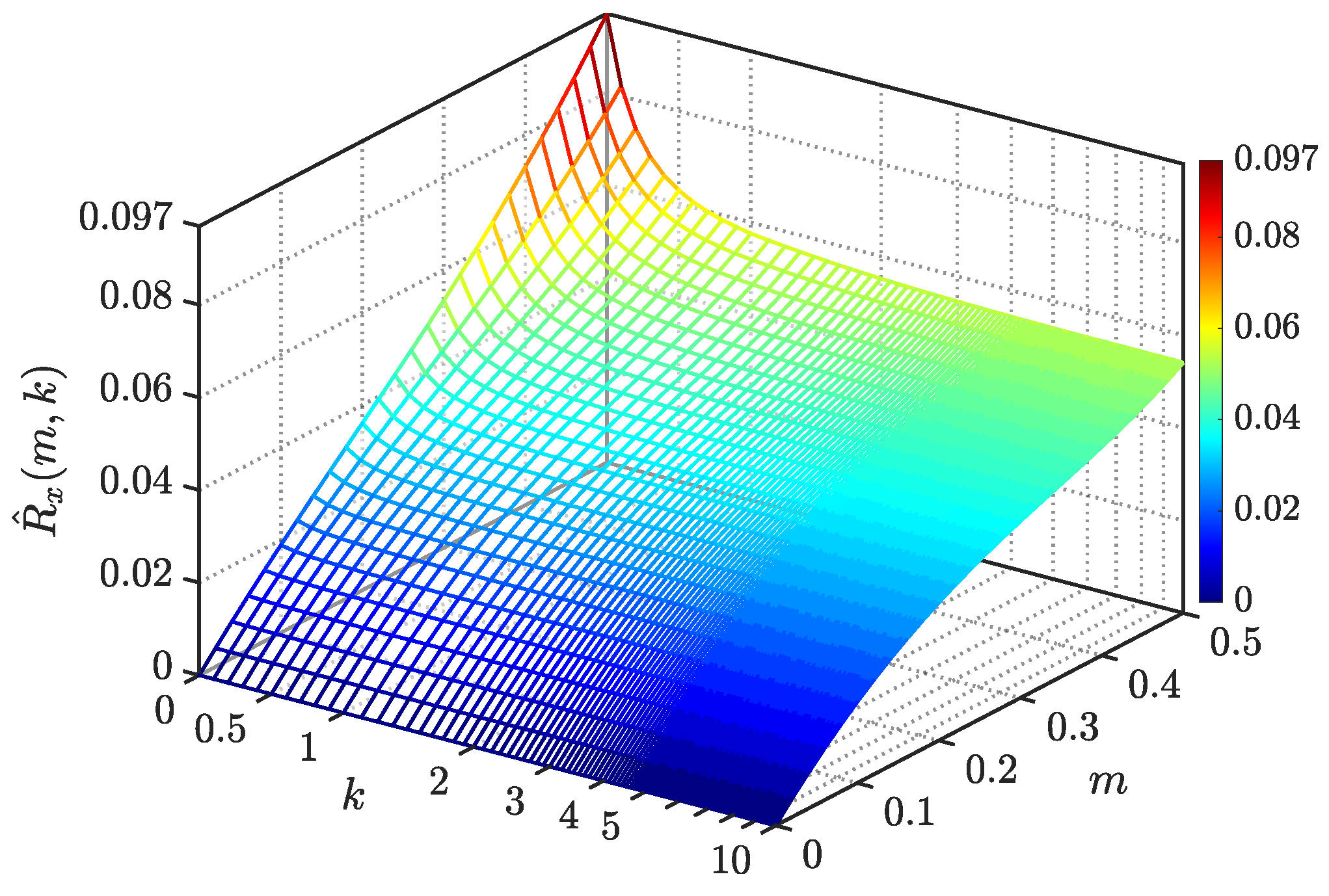
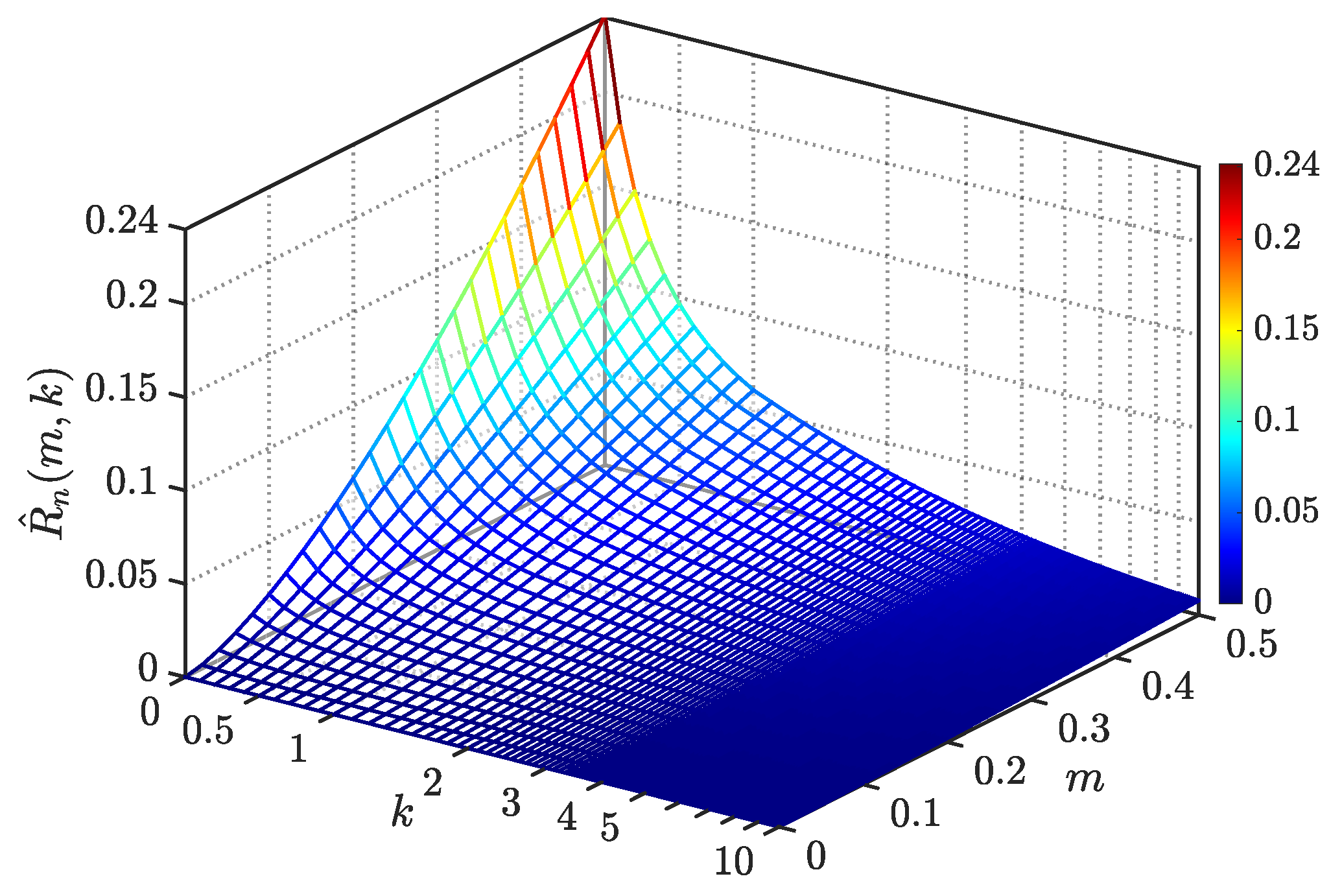
Figure 8, similar to Figure 6f, demonstrates the distribution of the normalized RMS value of phase current ripple in the whole linear modulation range depending on the particular design of the neutral line inductor. Unlike in Figure 6f, the RMS value of phase current ripple does not increase for k > 2, but instead, it gradually declines up to its limit at k = ∞ (three-leg VSC). That could be explained by the redistribution of current ripple magnitude (both primary and secondary) over one fundamental period. For example, from Figure 6d,e, it is quite evident that, even though the absolute magnitude of peak-to-peak phase current ripple increased in Figure 6e, the time diapason with relatively high current ripple magnitude decreased (areas around ϑ = 0 or ϑ = π/2).
Figure 9a–c demonstrate good matching between the normalized current ripple RMS calculated by Equation (27) and the corresponding values gained from simulations (true RMS) in the whole linear modulation index range. Moreover, Figure 9d illustrates a comparison of the normalized current ripple RMS as a function of modulation index m for several VSC topologies. In the legend of this plot, “3leg” stands for the three-leg converter configuration. Likewise, the other labels indicate the inductance value of the neutral line inductor in relation to the phase one for several designs of the four-leg converter. It can be noted that, for each converter configuration, the current ripple is almost the same for low modulation indexes (m 0.1), but the difference becomes noticeable for high modulation indexes. As expected, there is an evident drawback in terms of currents ripple when employing a four-leg converter over the three-leg counterpart in the case of balanced working conditions. In this instance, the 4th leg should be disconnected from the rest of the circuit to achieve the minimum current ripple RMS. However, it must be noted that the maximum RMS values of the current ripple in the four-leg VSCs with k = 1 and k = 2 are higher by only 6.25% and 2.17% than the corresponding value in the three-leg VSC, respectively.

4. Analysis of Neutral Current Ripple

4.1. Neutral Current Ripple Waveform

With reference to Equation (2), the neutral wire current can be obtained by summing the three phase currents. This also implies that the sum of the three phase fundamental current components is zero in the balanced current condition. Thus, there is no fundamental component in the neutral wire. On the other hand, it differs from zero in the case of unbalanced modulation/load. Unlike the fundamental component, the switching current ripple always circulates in the neutral wire, regardless of the modulation/load being balanced or not. Commonly, this ripple can be obtained by integrating the voltage across the neutral line inductor (cf. Equation (6)). However, at k = 0, this voltage is zero while the current ripple still flows through the neutral wire. Indeed, in that case, the ripple current is driven by the ripple component of “virtual neutral voltage”. The latter is the sum of the phase voltages. From Equation (7), it is evident that the current ripple in the neutral wire is inversely proportional to the k factor and directly proportional to the integral of “virtual neutral voltage”. The last term does not have a dependency on the k factor. Therefore, the variance of inductance in the neutral wire only affects the current ripple’s magnitude while its shape is not affected. Furthermore, the authors in [25] proved that the neutral current ripple does not depend on any abstract common mode injection in balanced modulation conditions. Similarly, it was shown that, in the case of SPWM (common mode injection is zero), the given equations are equally valid for any abstract unbalanced modulation. Figure 10 illustrates the voltage ripple component across the neutral line inductor at k = 1 and the corresponding neutral current ripple waveform in one switching period. This figure is an extension of Figure 2 with identical timeslots. As shown in the following subsection, the secondary (maximum local peaks) neutral ripple has a negligible small amplitude and does not contribute to the ripple’s true RMS calculation. Therefore, it is not considered in this analysis. Eventually, the “primary” and “secondary” notations are omitted for the neutral current ripple.
The normalized neutral current ripple envelope (peak) can be expressed by the following equation:
r ^ n , p k = ± 1 2 3 k + 1 x = a , b , c u x = ± 1 2 3 k + 1 x = a , b , c m x cos ϑ x
Equation (28) can be multiplied by normalization coefficient Vdc/(2Lfsw) to obtain the current ripple envelope in Ampere. Here and in the following expression of the normalized peak-to-peak neutral current ripple, dependency of the ripple function on variables m and ϑ is omitted since these functions include a sum term with all the modulating signals and represents a general case with all possible combinations of mx and ϑx.
To check the accuracy of Equation (28), Figure 11 presents the numerical simulation results for phase current unbalanced case depicted earlier in Figure 4c,d.
It is visible that, at k = 1, the neutral current ripple has an almost negligible variation of the ripple amplitude in a fundamental period (cf. Figure 11b). Therefore, in Figure 11a, it is quite hard to distinguish this deviation; thus, one may notice almost sinusoidal current ripple envelopes. Overall, it can be noted that the profile calculated by Equation (28) perfectly matches the instantaneous neutral current ripple profile. As it was pointed out above, the difference, in terms of neutral current ripple, among analyzed designs of the four-leg converters is only in the ripple’s amplitude while the shape is not affected. Therefore, in Figure 11, only one study case is plotted.
The peak-to-peak value of the ripple can be found as the double of its absolute peak value:
r ^ n , p p = 2 r ^ n , p k = 1 3 k + 1 x = a , b , c m x cos ϑ x
Figure 11a–d depict normalized peak-to-peak neutral current ripple profiles as a function of modulation index m and fundamental angle ϑ for several neutral line inductor designs in the analyzed four-leg converter. It is straightforward from Equation (29) that, with the k factor increase, the neutral current ripple dramatically decreases. Figure 12e shows the maximum peak-to-peak profile of the neutral current ripple that asymptotically approaches zero in the whole modulation range when k → ∞.
Figure 13 demonstrates similar results to those given above but in a more comparative way. The larger the inductance value of the neutral line inductor, the less evident the reduction in the neutral current ripple.

4.2. Neutral Current Ripple RMS

Similar to that in Section 3.2, RMS of the neutral current ripple in one switching period (cf. Figure 10) can be expressed as follows:
I ^ n m , ϑ , k | T s w = 2 3 T s w j = 0 4 i ^ n 2 t j + i ^ n t j i ^ n t j + 1 + i ^ n 2 t j + 1 t j
In Equation (30), the time point t 4 + 1 with reference to Figure 10 is the midpoint of the switching period. The time slots tj are expressed by Equations (12)–(14).
Different from the total RMS calculation of the phase current ripple in the fundamental period (cf. Section 3.2), the total RMS of the neutral current ripple due to ripple symmetry (cf. Figure 11b and Figure 12a–d) can be obtained by integration over just one sector, e.g., [0, p/6], leading to
I ^ n m , k = 6 π 0 π 6 I ^ x m , ϑ , k T s w I 2 d ϑ = V d c 2 L f s w   m 3 3 k + 1 2 3 2 π
Similar to what was done above, the normalization of (31) yields the following:
R ^ n m , k = m 3 3 k + 1 2 3 2 π
As mentioned earlier in Section 4.1, the neutral current ripple profile is independent from the common-mode injection signal. Thus, Equation (32) is valid for computing the neutral current ripple RMS in balanced PWM modulation regardless of the considered injection. Figure 14 depicts the distribution of the neutral current ripple RMS over linear modulation range and k factor values. Similar to the maximum peak-to-peak profile of the neutral current ripple (cf. Figure 12e), its RMS asymptotically approaches zero in the whole modulation range when k → ∞. Figure 15 demonstrates that, the larger the inductance value of the neutral line inductor, the less evident the reduction in the neutral current ripple (with k > 2, the RMS becomes almost negligible).
To verify the applicability of Equation (32), simulation results were plotted above the analytical traces in Figure 15. It is visible that the analytical functions (solid lines) perfectly match the numerical results (markers).

5. Performance Comparison and Design Example

5.1. Performance Comparison

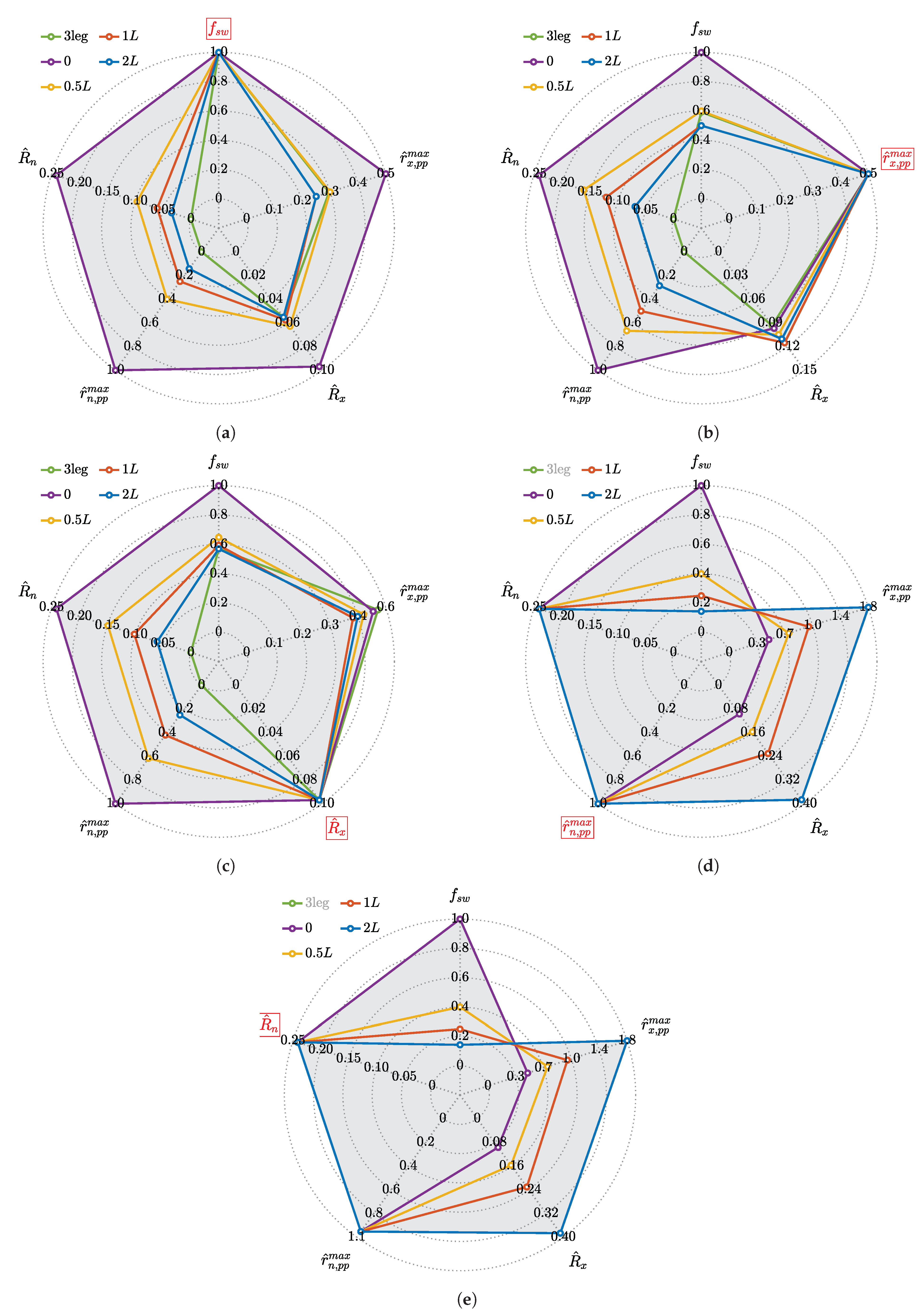
The findings presented above demonstrate, in a somewhat scattered way, the differences in AC current-ripple-related performance between a typical three-leg voltage source converter and its four-leg counterparts with or without a neutral line inductor. To summarize the AC current ripple properties and to give a little more insight into how these characteristics correlate with each other, a set of Kiviat (radar) diagrams is depicted in Figure 16. To compose the subplots, five metrics were considered, namely switching frequency (fsw), maximum normalized peak-to-peak values of phase ( r ^ x , p p m a x ), neutral ( r ^ n , p p m a x ) switching current ripples, normalized RMS values of phase ( R ^ x ), and neutral ( R ^ n ) switching current ripples. To perform this comparison, the following working point was selected, namely unity power factor (φ = 0) and m = 0.5 (balanced case).
One metric per time was equalized in the five depicted subcases, with the maximum corresponding characteristic of other VSC configurations permitting us to relate the remaining parameters. The aligned characteristics are displayed in the red box. The metrics equalization can be achieved by tuning the operating switching frequency, as visible from Figure 16b–e, where fsw ≠ 1 p.u. In this context, other equalizations are possible, e.g., by varying interface inductance or DC-link voltage. Table 2 summarizes the aforementioned characteristics with the same switching frequency for all the compared topologies.
In these subplots’ legend, “3leg” stands for a three-leg (k = ∞) converter. Similarly, the other traces represent characteristics for a four-leg voltage source converter (by default, the abbreviation “4leg” was omitted for shorter notation) without (“0”) or with (“0.5L”, “1L”, and “2L”) a neutral line inductor. Figure 16d,e do not contain a “3leg” trace since, in this VSC configuration, the fourth wire and the corresponding current ripple properties are absent. Figure 16a illustrates the measures at the fixed, identical switching frequency, which is precisely the case presented above. It is quite evident from this subplot that, operating in a balanced three-phase mode, the 4th leg of a four-leg VSCs should be disconnected from the rest of the circuit since it causes not only additive power losses in the neutral wire but also excessive losses and an overall worse harmonic pollution in the phases. Even though, for some four-leg VSC arrangements, it is possible to obtain a lower peak-to-peak current ripple (k > 1/√3), the lowest possible ripple RMS among compared configurations is precisely in the three-leg converter. By fixing the maximum normalized peak-to-peak value of phase current ripple at its common maximum level, the subplot given in Figure 16b can be obtained. It is interesting to notice that, with the same maximum peak-to-peak and very similar RMS values of phase current ripple in both the three-leg converter and four-leg VSC without a neutral line inductor, the switching frequency in the three-leg case can be cut down by 42.26%. In this context, the frequency reduction in the four-leg topology with neutral inductance value “0.5L” is 40%. In fact, to reach a similar current ripple performance in terms of maximum peak-to-peak value, the neutral inductance value should be set to Ln = 1/√3L ≈ 0.5774L. Any value of the k factor in the range [1/√3, 1] will reduce the phase ripple maximum peak-to-peak with respect to the three-leg configuration. As shown above (cf. Figure 6f), further increase in the k factor up to 2 does not affect the maximum peak-to-peak phase current ripple while the other current-ripple-related measures decrease (cf. Figure 8, Figure 12 and Figure 14). Any value of the k factor greater than 2 will degrade the phase ripple’s maximum peak-to-peak performance. On the other hand, with fixed phase ripple RMS values at the same level (cf. Figure 16c), the aforementioned switching frequency reduction between the four-leg VSC without neutral line inductor (“0”) and its three-leg counterpart is about 44.28%. Simultaneously, in this study case, the absolute switching frequency difference between the “1L” four-leg VSC configuration and the “3leg” converter is only 3.74%. Figure 16d,e represent events, respectively, when the maximum normalized peak-to-peak and RMS values of neutral current ripple are fixed at the highest common level. The two subplots look similar since the fixed quantities have identical linear dependences on the k factor. Nevertheless, these figures depict the performance “gaps” between the compared four-leg VSC configurations.
Other VSC design parameters, such as DC-link voltage and interface inductor size, can be alternate in a similar way. However, since all of them have a linear dependency on the ripple functions described above, the graphs in Figure 16 have a similar look. In fact, the authors of [22] provide an intuitive comparison between different inductor designs in a four-leg VSC. The authors claim that the inductor’s design with k = 0.5 showed better output voltage THD while a combined inductor area product (normally a Cu–Fe product) is 38% smaller than the case with k = 0. The authors in [23] validated that, in the four-leg VSC arrangement with k = 1, the smallest amplitude of the load neutral point voltage can be obtained. In the present analysis, to demonstrate the derived expressions’ application and to validate an optimal inductor selection, a design example is introduced in the following subsection.

5.2. Design Example

This subsection provides a design example of the three-phase, four-wire power factor correction (PFC) stage of an on-board charger (OBC) for EVs. The sinusoidal PWM method was applied to the referred PFC. Although this example concentrated on the three-phase converter design, a similar approach is applicable for the single-phase case at k = 0. The derived equations for the phase AC current ripple are independent from the other phase currents. At this point, the current ripple in the neutral is the same as in the phase. Likewise, the phase AC current ripple equations are relevant for the well-known three-phase, three-leg VSCs by merely setting the k factor to infinity. The initial design parameters for the PFC stage of an OBC are summarized in Table 3.
Given the rated values of the converter active power and grid line-to-line RMS voltage, the rated RMS value of phase current is I = P/(√3Vac) ≈ 16 A. Therefore, the maximum allowed peak-to-peak value of phase current ripple is as follows:
i ^ x , p p m a x = Δ i ^ x , p p m a x 100   2 I = 10 100 16   2 = 2.263   A
Combining Equations (15) and (33) and solving for inductance value L yields the following:
L | m a x , p p = V d c 2   i ^ x , p p m a x   f s w   r ^ x , p p m a x =   1000 2 · 2.263 · 100 · 10 3 0.25 = 552.4   μ H
where L | m a x , p p is the minimum required inductance of the phase inductors to keep the corresponding peak-to-peak value of phase current ripple in the prescribed boundary. Here, the DC-link voltage is set to its maximum value from the defined range since it corresponds to the current ripple’s maximum value. Similarly, the maximum value of the peak-to-peak phase current ripple function is calculated at the highest modulation index and required value of k (in this computation, the reference is made to k = 1). The latter quantity can be simply taken from Figure 6f at m = 0.5 and the specific k factor.
Now, based on the precalculated value of phase inductance, one can directly compute phase current THD composed by the switching process:
T H D = I ^ x I   100 % = V d c 2 L f s w   R ^ x I   100 % =   1000 · 100 % 2 · 552.4 · 10 6 · 100 · 10 3   0.0576 16 = 3.26 %
Although this value complies with the IEEE 519-2014 standard (<5% 1 kV) for grid-connected applications, let us say that there is a particular requirement to reach ≤ 3% level. In this case, it is possible, similar to Equation (34), to recalculate inductance value by having a restricted RMS value of phase current ripple as follows:
L | r m s = V d c 2   I ^ x   f s w   R ^ x =   1000 2 · 0.48 · 100 · 10 3   0.0576 = 600.1   μ H
where L | r m s is the minimum required inductance of the phase inductors to keep the corresponding RMS value of phase current ripple in the prescribed boundary. The restricted RMS value of phase current ripple was obtained from (35).
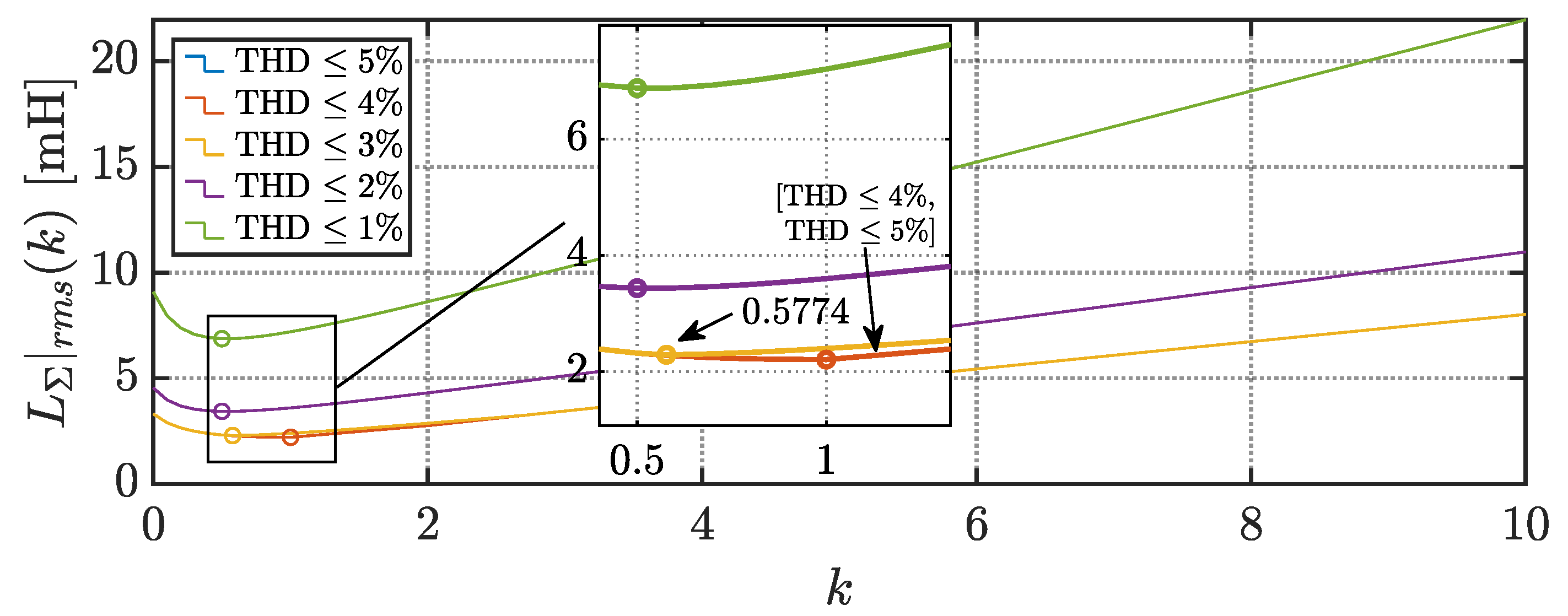
Table 4 summarizes the above calculated quantities for different VSC configurations. The columns labeled as “ T H D | m a x , p p ” and “ T H D | r m s ” demonstrate the THD values of AC current by applying the corresponding phase inductances L | m a x , p p and L | r m s that are explained above. The green and red background colors in the “THD” columns emphasize the THD values that respect or overpass the restricted ≤3% level. In this table, an additional four-leg VSC design (“0.5774L”) was performed to demonstrate the value of inductance that should be placed in the neutral wire to achieve precisely the same amplitude of maximum peak-to-peak phase ripple as it is in the three-leg topology while maintaining identical inductors in the phases. On the other hand, if someone is interested in obtaining the minimum possible total installed inductance in the four-leg VSC configuration while obtianing enhanced current ripple performance with respect to the other four-leg VSC designs, Figure 17 depicts some related study cases with respect to the different restricted THD levels (from 5 to 1%). The total installed inductance can be considered a metric relative to the converter’s cost, weight, and volume, and therefore as a rule should be minimized. If it is restricted by certain THD levels, it can be formulated by
L Σ | r m s = 3 + k L | r m s =   3 + 1   ·   600.1 = 2.4004   mH
In this design example, keeping THD level within approximately 4%, the dominant role gives the maximum peak-to-peak phase current ripple limit. Therefore, minimum total installed inductance is found at k = 1. At this point, with the same maximum peak-to-peak phase ripple, this inductance value is only 13.4% higher than the total installed inductance in the three-leg topology. On the other hand, with lower THD bondary levels, the minimum total installed inductance value appears at lower k factors. For instance, at THD ≤ 3%, the lowest L Σ | r m s belongs to the “0.5774L” four-leg VSC design. For even lower THD levels, the k factor tends toward 0.5. It is also interesting to notice that this minimum total installed inductance relation between diffent four-leg VSC designs is the same as long as the specific maximum peak-to-peak phase current ripple (in % fundamental) has the same magnitude limit. This observation can be formulated due to the fact that the amplitude of the current fundamental component, DC-link voltage, and switching frequency are only scaling factors while L Σ has a dependency on maximum normalized peak-to-peak phase current ripple function r ^ x , p p m a x or/and normalized phase current ripple RMS fuction R ^ x . These two should be considered together if both restrictions are imposed; otherwise, they could be treated independently.
Other design parameters, such as DC-link voltage and switching frequency, can be tuned similarly to the converter’s interface inductance.
All in all, by comparing all the design aspects, including current ripple characteristics, the grid code restriction (THD < 5% 1 kV), and total installed inductance, among studied four-leg configurations, the optimal one would be the four-leg VSC with a neutral line inductor sized exactly as the phase counterparts. However, this claim can be further argued depending on the design constraints.

6. Experimental Results

The theoretical findings were verified by experimental tests carried out with the setup shown in Figure 18. The experimental setup consists of the four-leg VSC topology connected to the three-phase RC circuit (cf. Figure 3). The DC side of the VSC is connected to an adjustable DC supply (GEN100-33, TDK- Lambda Corporation, Tokyo, Japan). The VSC itself is formed by two insulated-gate bipolar transistor (IGBT) power modules (PS22A76, Mitsubishi Electric Corporation, Tokyo, Japan). The interface air-core inductors have identical characteristics and are placed in the phases and neutral links to form a “1L” structure. On the other hand, to build “0.5L” and “2L” configurations, an additional identical air-core inductor was placed in parallel or series with the neutral one, respectively. In this way, the neutral line inductor’s total internal resistance can be represented as a multiple of k factor, similar to its inductance. The implemented RLC passive circuit provides an opportunity to focus solely on switching current ripples with open-loop AC voltage regulation without a closed-loop current controller. As a result, a wide range of balanced and unbalanced modulation cases can be studied by merely varying the characteristics of modulating signals. The current and voltage measurements were performed using current sensors (LA 55-P, LEM Europe GmbH, Fribourg, Switzerland) and isolated differential voltage probes (PICO TA057, Pico, Tyler, TX, USA). The power modules were driven by the digital signal processor (DSP) microcontroller board (TMS320 F28379D, Texas Instruments, Dallas, TX, USA) via intermediate optical links. Modulation indices were changed in real-time via the MATLAB/Simulink (MathWorks, Natick, MA, USA) platform in the external mode. The experimental setup’s main parameters were the same as for the simulations performed above and are summarized in Table 1.
The measured currents and voltages were initially acquired and processed as a set of sampled data points via two digital oscilloscopes (DS1054Z, Rigol, Beijing, China). The sampling frequency for all scope channels were fixed at 5 MHz. The results visualization was accomplished via MATLAB environment. No signal filtering was applied. Phase and neutral currents for compared four-leg configurations were acquired using the same setup, changing only the arrangement in the neutral inductor. In all the cases, a balanced modulation was implemented with modulation index m = 0.5.
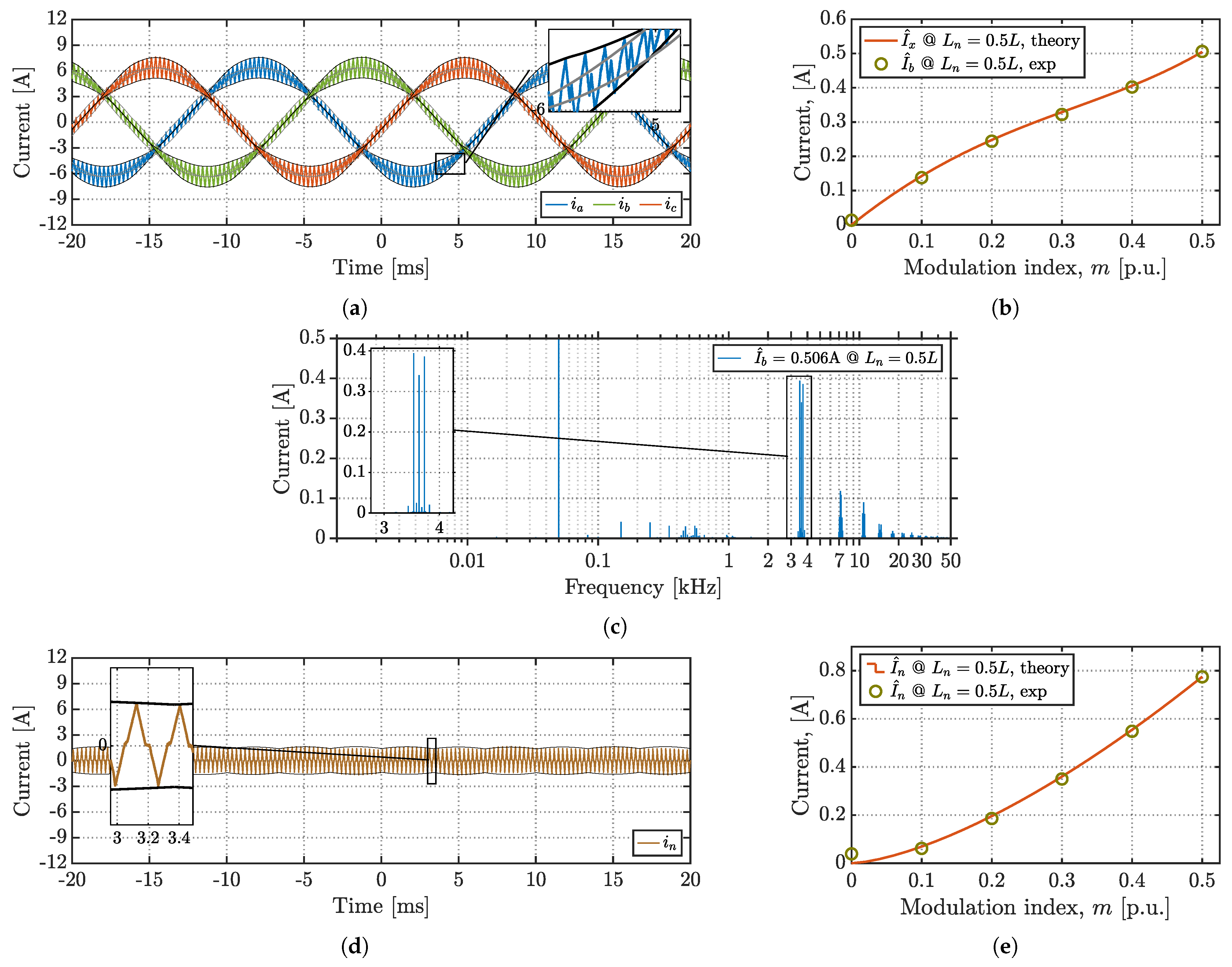
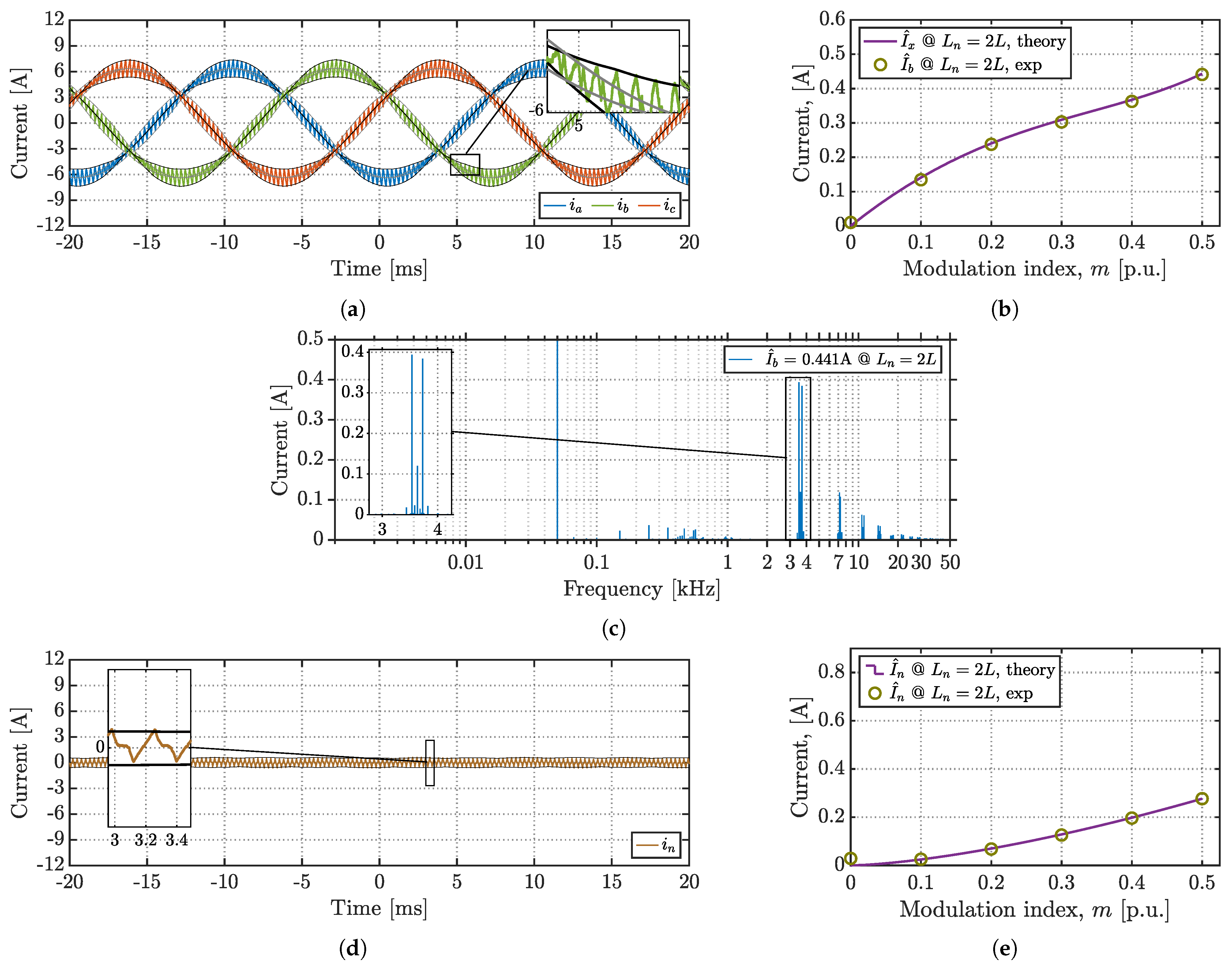
From Figure 19, Figure 20 and Figure 21, the acquired experimental current waveforms along with bounding primary (black) and secondary (gray) envelopes (cf. subfigures “(a)” and “(d)”), RMS values of current ripples at certain modulation indices (cf. subfigures “(b)” and “(e)”), and harmonic spectrum of a phase current (ph. b) are depicted. These figures represent several four-leg configurations depending on the value of inductance in the neutral wire, namely “0.5L”, “1L”, and “2L”. It is evident from the figures that both primary and secondary envelopes correctly bond the phase current profiles for all implemented topological cases (cf. subfigures “(a)”). A similar observation can be made from the plot that depicts neutral current (cf. subfigures “(d)”). Even though the neutral wire’s fundamental current component is zero, due to balanced operation, the ripple component is still there and composed by a sum of phase current ripples (ph. a, b, and c). Validation of the derived expressions is based on a comparison of the measured and expected RMS values of current ripple rather than the associated current THDs since the measured THDs can include other harmonics that are non-related to the switching process. In this context, the THD comparison is not strictly fair. For instance, low-frequency harmonics can be observed in the depicted harmonic spectrums (cf. subfigures “(b)”) within the frequency range 0.1-1 kHz, and they are mainly due to imperfect load symmetry, presence of dissimilar dead-times among converter legs, uncertainties in measuring tools and some other nonlinearities. Apart from these negligible low-frequency harmonics in the laboratory setup, the dominant harmonics are around fsw, 2fsw, and 3fsw. By comparing phase current harmonic spectrum from different subcases (cf. subfigures “(c)”), it can be noticed that substantial magnitude reduction experience only harmonics at fsw. In contrast, the other either practically unchanged (e.g., sidebands at fsw) or have a barely noticeable drop. The RMS values of phase (cf. subfigures “(b)”) and neutral (cf. subfigures “(e)”) currents measured at several points of linear modulation range have a reasonable match with the predicted values. The discrepancy observed at m = 0 can be explained by noise dominance in unloaded setup and higher uncertainties of measurement tools at this current level. Altogether, the obtained experimental results prove the applicability and high accuracy of derived current ripple expressions.

7. Conclusions

This paper provides a thorough analysis of the instantaneous (switching) AC current ripple in the general case of three-phase, four-leg inverters with a neutral line inductor. The study covers both phase and neutral current ripple characteristics in the case of balanced sinusoidal PWM. All these properties are equally valid for either balanced or unbalanced current conditions provoked by grid/load. Generalized expressions of the peak and peak-to-peak values of phase current ripple are derived in the whole fundamental period as functions of modulation index m, fundamental angle ϑ, and k factor. The latter characteristic represents the ratio between the value of neutral inductance and its phase counterpart. This coefficient can vary from zero to infinity. Therefore, using derived AC current ripple properties as a function of the k factor allows us to apply them in a large group of three-phase, two-level converter designs. These converter structures include four-leg converters with or without a neutral line inductor and a conventional three-leg inverter. It was demonstrated thatm in some designs of the four-leg VSC with a neutral line inductor, the maximum peak-to-peak value of the phase current ripple is considerably lower at higher modulation indices with respect to the classical three-leg converter. Furthermore, based on the current ripple distribution over the fundamental period, another key characteristic, namely the current ripple RMS, was determined as a modulation index and k factor function. Similar current ripple properties were obtained for the neutral. Based on these expressions, one can easily determine the required value of interface inductors, both in phases and the neutral, can estimate the AC current THD induced by the converter’s switching process at any certain operating point, and can check its compliance with the associated standard. The derived equations are simple, powerful, and ready for accurate AC current ripple calculations without running computationally heavy repetitive numerical simulations. To demonstrate the given formulations’ effectiveness, a design example for the PFC stage of EV on-board chargers is provided. In addition to that, a comparative analysis between several designs is presented. This study helps to define a range of optimal neutral line inductances or to estimate a reduction in switching frequency/line inductance values by fixing one of the current ripple characteristics. All the presented theoretical expressions were broadly validated through both numerical simulations and laboratory tests. The achieved results demonstrate an adequate match with the analytical derivations.

Author Contributions

Conceptualization, A.V., R.M., M.H., M.R. and G.G.; methodology, A.V., R.M. and G.G.; software, A.V. and R.M.; validation, A.V., R.M., M.H. and M.R.; formal analysis, A.V., R.M. and G.G.; investigation, A.V. and R.M.; resources, A.V., R.M., M.H. and M.R.; data curation, A.V. and R.M.; writing—original draft preparation, A.V., R.M., M.H. and M.R.; writing—review and editing, A.V., R.M., M.H., M.R. and G.G.; visualization, A.V. and R.M.; supervision, M.R. and G.G. All authors have read and agreed to the published version of the manuscript.

Funding

This research received no external funding.

Institutional Review Board Statement

Not applicable.

Informed Consent Statement

Not applicable.

Data Availability Statement

The data are available in the paper.

Conflicts of Interest

The authors declare no conflict of interest.

References

  1. Zhong, Q.-C. Power-Electronics-Enabled Autonomous Power Systems: Architecture and Technical Routes. IEEE Trans. Ind. Electron. 2017, 64, 5907–5918. [Google Scholar] [CrossRef]
  2. Yilmaz, M.; Krein, P.T. Review of Battery Charger Topologies, Charging Power Levels, and Infrastructure for Plug-In Electric and Hybrid Vehicles. IEEE Trans. Power Electron. 2013, 28, 2151–2169. [Google Scholar] [CrossRef]
  3. Brenna, M.; Foiadelli, F.; Leone, C.; Longo, M. Electric Vehicles Charging Technology Review and Optimal Size Estimation. J. Electr. Eng. Technol. 2020, 15, 2539–2552. [Google Scholar] [CrossRef]
  4. Dong, G.; Ojo, O. Current Regulation in Four-Leg Voltage-Source Converters. IEEE Trans. Ind. Electron. 2007, 54, 2095–2105. [Google Scholar] [CrossRef]
  5. Shekari, T.; Golshannavaz, S.; Aminifar, F. Techno-Economic Collaboration of PEV Fleets in Energy Management of Microgrids. IEEE Trans. Power Syst. 2016, 32, 3833–3841. [Google Scholar] [CrossRef]
  6. Viatkin, A.; Hammami, M.; Grandi, G.; Ricco, M. Analysis of a Three-Phase Four-Leg Front-End Converter for EV Chargers with Balanced and Unbalanced Grid Currents. In Proceedings of the IECON 2019-45th Annual Conference of the IEEE Industrial Electronics Society, Lisbon, Portugal, 14–17 October 2019; Volume 1, pp. 3442–3449. [Google Scholar]
  7. Lin, Z.; Ruan, X.; Jia, L.; Zhao, W.; Liu, H.; Rao, P. Optimized Design of the Neutral Inductor and Filter Inductors in Three-Phase Four-Wire Inverter With Split DC-Link Capacitors. IEEE Trans. Power Electron. 2019, 34, 247–262. [Google Scholar] [CrossRef]
  8. Nascimento, C.F.; Diene, O.; Watanabe, E.H. Analytical model of three-phase four-wire VSC operating as grid forming power converter under unbalanced load conditions. In Proceedings of the 2017 IEEE 12th International Conference on Power Electronics and Drive Systems (PEDS), Honolulu, HI, USA, 12–15 December 2017; pp. 1219–1224. [Google Scholar]
  9. Hintz, A.; Prasanna, U.R.; Rajashekara, K. Comparative Study of the Three-Phase Grid-Connected Inverter Sharing Unbalanced Three-Phase and/or Single-Phase systems. IEEE Trans. Ind. Appl. 2016, 52, 5156–5164. [Google Scholar] [CrossRef]
  10. Zhao, W.; Ruan, X.; Yang, D.; Chen, X.; Jia, L. Neutral Point Voltage Ripple Suppression for a Three-Phase Four-Wire Inverter With an Independently Controlled Neutral Module. IEEE Trans. Ind. Electron. 2017, 64, 2608–2619. [Google Scholar] [CrossRef]
  11. Fu, Y.; Li, Y.; Huang, Y.; Lu, X.; Zou, K.; Chen, C.; Bai, H. Imbalanced Load Regulation Based on Virtual Resistance of A Three-Phase Four-Wire Inverter for EV Vehicle-to-Home Applications. IEEE Trans. Transp. Electrif. 2018, 5, 162–173. [Google Scholar] [CrossRef]
  12. Zhang, R.; Prasad, V.; Boroyevich, D.; Lee, F. Three-dimensional space vector modulation for four-leg voltage-source converters. IEEE Trans. Power Electron. 2002, 17, 314–326. [Google Scholar] [CrossRef]
  13. Hava, A.; Kerkman, R.; Lipo, T. Carrier-based PWM-VSI overmodulation strategies: Analysis, comparison, and design. IEEE Trans. Power Electron. 1998, 13, 674–689. [Google Scholar] [CrossRef] [Green Version]
  14. Hava, A.M.; Kerkman, R.J.; A Lipo, T. Simple analytical and graphical methods for carrier-based PWM-VSI drives. IEEE Trans. Power Electron. 1999, 14, 49–61. [Google Scholar] [CrossRef]
  15. Holmes, D.G.; Lipo, T.A. Pulse Width Modulation for Power Converters: Principles and Practice; John Wiley & Sons: Hoboken, NJ, USA, 2003. [Google Scholar]
  16. Jiang, D.; Wang, F. Current-Ripple Prediction for Three-Phase PWM Converters. IEEE Trans. Ind. Appl. 2013, 50, 531–538. [Google Scholar] [CrossRef]
  17. Grandi, G.M.; Loncarski, J. Evaluation of current ripple amplitude in three-phase PWM voltage source inverters. In Proceedings of the 2013 International Conference-Workshop Compatibility And Power Electronics, Ljubljana, Slovenia, 5–7 June 2013; pp. 156–161. [Google Scholar]
  18. Jiang, D.; Wang, F. Study of analytical current ripple of three-phase PWM converter. In Proceedings of the 2012 Twen-ty-Seventh Annual IEEE Applied Power Electronics Conference and Exposition (APEC), Orlando, FL, USA, 5–9 February 2020; pp. 1568–1575. [Google Scholar]
  19. Grandi, G.; Loncarski, J.; Seebacher, R. Effects of current ripple on dead-time distortion in three-phase voltage source inverters. In Proceedings of the 2012 IEEE International Energy Conference and Exhibition (ENERGYCON), Florence, Italy, 9–12 September 2012; pp. 207–212. [Google Scholar]
  20. Hammami, M.; Ricco, M.; Viatkin, A.; Mandrioli, R.; Grandi, G. Evaluation of AC Current Ripple in case of SplitCapacitor Three-Phase Four Wires Inverters. In Proceedings of the 2020 6th IEEE International Energy Conference (ENERGYCon), Gammarth, Tunisia, 28 September–1 October 2020; pp. 128–132. [Google Scholar]
  21. Cai, W.; Shen, Y.; Xiao, X.; Wang, W.; Zhang, W.; Li, K.; Zhang, C.; Zhao, Z. Design of the Neutral Line Inductor for Three-phase Four-leg Inverters. In Proceedings of the 2019 IEEE Sustainable Power and Energy Conference (iSPEC), Beijing, China, 21–23 November 2019; pp. 2455–2460. [Google Scholar]
  22. Jahns, T.; De Doncker, R.; Radun, A.; Szczesny, P.; Turnbull, F. System design considerations for a high-power aerospace resonant link converter. IEEE Trans. Power Electron. 1993, 8, 663–672. [Google Scholar] [CrossRef]
  23. Liu, Z.; Liu, J.; Li, J. Modeling, Analysis, and Mitigation of Load Neutral Point Voltage for Three-Phase Four-Leg Inverter. IEEE Trans. Ind. Electron. 2012, 60, 2010–2021. [Google Scholar] [CrossRef]
  24. Viatkin, A.; Mandrioli, R.; Hammami, M.; Ricco, M.; Grandi, G. Theoretical Analysis of the AC Current Ripple in Three-Phase Four-Leg Sinusoidal PWM Inverters. In Proceedings of the 2020 IEEE 29th International Symposium on Industrial Electronics (ISIE), Delft, The Netherlands, 17–19 June 2020; pp. 796–801. [Google Scholar]
  25. Mandrioli, R.; Viatkin, A.; Hammami, M.; Ricco, M.; Grandi, G. A Comprehensive AC Current Ripple Analysis and Performance Enhancement via Discontinuous PWM in Three-Phase Four-Leg Grid-Connected Inverters. Energies 2020, 13, 4352. [Google Scholar] [CrossRef]
Figure 1. General circuit scheme of a three-phase, four-leg voltage-source converter with a neutral line inductor.
Energies 14 01430 g001
Figure 2. Generic case of the sinusoidal pulse-width modulation (SPWM) strategy (top), pole voltages of the three-phase inverter and high-frequency voltage component v ^ a o (middle), and phase a current ripple waveform in one switching period (bottom).
Energies 14 01430 g002
Figure 3. Test circuit scheme of a three-phase, four-leg voltage-source converter with a neutral line inductor connected to an AC load.
Energies 14 01430 g003
Figure 4. Normalized unbalanced phase currents along with their primary (black) and secondary (gray) current ripple envelopes (a,c,e) m = 0.5 and corresponding normalized switching current ripples in phase a with their respective primary (black) and secondary (gray) envelopes, (b,d,f) k = 0.5 (upper plots (a,b)), k = 1 (middle plots (c,d)), and k = 2 (bottom plots (e,f)).
Energies 14 01430 g004
Figure 5. Normalized unbalanced phase currents along with their primary (black) and secondary (gray) current ripple envelopes (a,c,e) m = 0.4 and corresponding normalized switching current ripples in phase a with their respective primary (black) and secondary (gray) envelopes and (b,d,f) k = 0.5 (upper plots (a,b)), k = 1 (middle plots (c,d)), and k = 2 (bottom plots (e,f)).
Energies 14 01430 g005
Figure 6. Maximum profiles of normalized peak-to-peak primary and secondary phase switching current ripple envelopes in the case of SPWM: (a) k = 0, (b) k = 0.5, (c) k = 1, (d) k = 2, and (e) k = ∞; maximum normalized peak-to-peak phase switching current ripple as a function of modulating index m and k factor (f,g).
Energies 14 01430 g006
Figure 7. Maximum, normalized, peak-to-peak phase switching current ripple as a function of modulation index m at specific inductance values of a neutral line inductor.
Energies 14 01430 g007
Figure 8. The normalized RMS value of phase switching current ripple as a modulating index m and k factor function.
Energies 14 01430 g008
Figure 9. Normalized, theoretical RMS value of phase switching current ripple as a function of modulation index m along their corresponding simulation counterparts (a) k = 0.5, (b) k = 1, and (c) k = 2 and (d) a comparison of the normalized RMS of a phase switching current ripple.
Energies 14 01430 g009
Figure 10. Voltage ripple component across the neutral line inductor (top) and neutral current ripple waveform in one switching period (bottom).
Energies 14 01430 g010
Figure 11. Profile and primary (black) envelope m = 0.5 and k = 1: (a) normalized neutral current; (b) normalized neutral current ripple.
Energies 14 01430 g011
Figure 12. Normalized, peak-to-peak neutral switching current ripple envelopes in case of SPWM (a) k = 0, (b) k = 0.5, (c) k = 1, and (d) k = 2 and (e) maximum, normalized, peak-to-peak neutral switching current ripple as a function of modulating index m and k factor.
Energies 14 01430 g012
Figure 13. Maximum, normalized, peak-to-peak neutral switching current ripple as a function of modulation index m at specific inductance values of the neutral line inductor.
Energies 14 01430 g013
Figure 14. The normalized RMS value of a neutral switching current ripple as a function of modulating index m and k factor.
Energies 14 01430 g014
Figure 15. The normalized RMS value of the neutral switching current ripple as a function of modulation index m at specific inductance values of neutral line inductor.
Energies 14 01430 g015
Figure 16. Kiviat (radar) diagrams depicting current-ripple-related performances for compared converter topologies at φ = 0 and m = 0.5 and identical fixed metrics: (a) switching frequency; (b) maximum, normalized, peak-to-peak phase switching current ripple; (c) normalized RMS value of a phase switching current ripple; (d) maximum, normalized, peak-to-peak neutral switching current ripple; and (e) normalized RMS value of neutral switching current ripple.
Energies 14 01430 g016
Figure 17. Converter’s total installed inductance and its optimal point at several THD limits.
Energies 14 01430 g017
Figure 18. Experimental laboratory setup.
Energies 14 01430 g018
Figure 19. Experimental measurements of three-phase and neutral currents m = 0.5 and k = 0.5: (a) balanced three-phase currents along with their primary (black) and secondary (gray) current ripple envelopes, (b) RMS values of a phase current ripple (ph. b), (c) harmonic spectrum of a phase current (ph. b), (d) neutral current along with its current ripple envelope (black), and (e) RMS values of the neural current ripple.
Energies 14 01430 g019
Figure 20. Experimental measurements of three-phase and neutral currents m = 0.5 and k = 1: (a) balanced three-phase currents along with their primary (black) and secondary (gray) current ripple envelopes, (b) RMS values of a phase current ripple (ph. b), (c) harmonic spectrum of a phase current (ph. b), (d) neutral current along with its current ripple envelope (black), and (e) RMS values of the neural current ripple.
Energies 14 01430 g020aEnergies 14 01430 g020b
Figure 21. Experimental measurements of three-phase and neutral currents m = 0.5 and k = 2: (a) balanced three-phase currents along with their primary (black) and secondary (gray) current ripple envelopes, (b) RMS values of a phase current ripple (ph. b), (c) harmonic spectrum of a phase current (ph. b), (d) neutral current along with its current ripple envelope (black), and (e) RMS values of the neural current ripple.
Energies 14 01430 g021
Table 1. System parameters.
ParameterValue
Rated DC voltage, Vdc (V)100
Ac-link inductor parameters: L (mH), R (Ω)1.73, 0.727
Passive load parameters: Co (μF), Ro (Ω)
- balanced45, 6.6
- unbalanced (ph. a/b/c)51, 5.9/21, 9.2/11, 12.4
Power factor (50 Hz)1
Switching frequency, fsw (kHz)3.6
Table 2. Current-ripple-related data for the case of the same switching frequency φ = 0 and m = 0.5.
VSC ArchitectureLabel f s w r ^ x , p p m a x R ^ x r ^ n , p p m a x R ^ n
Three-leg, Ln = ∞3leg10.28870.054--
Four-leg without
neutral line inductor
010.50.096910.2414
Four-leg with neutral
line inductor, Ln = 0.5L
0.5L10.30.06280.40.0965
Four-leg with neutral
line inductor, Ln = 1L
1L10.250.05760.250.0603
Four-leg with neutral
line inductor, Ln = 2L
2L10.250.05520.14290.0345
Table 3. Design parameters of the three-phase power factor correction (PFC) stage of an on-board charger (OBC).
ParameterValue
Rated active power, P (kW)11
Rated RMS value of grid line-to-line voltage, Vac (V)400
Dc voltage range, Vdc (V)700–1000
Switching frequency, fsw (kHz)100
Maximum peak-to-peak phase current ripple, Δ i ^ x , p p m a x (% of fundamental)10
Table 4. Inductor design at the same switching frequency.
VSC ArchitectureLabel L | m a x , p p   ( µ H ) T H D | m a x , p p   ( % ) L | r m s   ( µ H ) T H D | r m s   ( % ) L n | r m s   ( µ H )
Three-leg, Ln = ∞3leg637.92.64637.92.64-
Four-leg without
neutral line inductor
01104.92.741104.92.74-
Four-leg with neutral
line inductor, Ln = 0.5L
0.5L662.92.96662.92.96331.5
Four-leg with neutral
line inductor, Ln = 1/√3L
0.5774L637.93.01640.63.0369.9
Four-leg with neutral
line inductor, Ln = 1L
1L552.43.26600.13.0600.1
Four-leg with neutral
line inductor, Ln = 2L
2L552.43.125753.01150
Publisher’s Note: MDPI stays neutral with regard to jurisdictional claims in published maps and institutional affiliations.