Article

LCC-S-Based Integral Terminal Sliding Mode Controller for a Hybrid Energy Storage System Using a Wireless Power System

1
School of Electrical Engineering, Shandong University, Jinan 250061, China
2
School of Electrical Engineering and Computer Science, National University of Sciences and Technology, Islamabad 44000, Pakistan
3
Energy Research Institute, Qilu University of Technology, Shandong Academy of Sciences, Jinan 250353, China
*
Author to whom correspondence should be addressed.
Energies 2021, 14(6), 1693; https://doi.org/10.3390/en14061693
Submission received: 13 February 2021 / Revised: 11 March 2021 / Accepted: 15 March 2021 / Published: 18 March 2021
(This article belongs to the Special Issue Research on Wireless Power Transfer System)

Abstract

:
Unlike the plug-in charging system, which has safety concerns such as electric sparks, wireless power transfer (WPT) is less-time consuming, is environmentally friendly and can be used in a wet environment. The inclusion of hybrid energy storage systems (HESSs) in electric vehicles (EVs) has helped to increase their energy density as well as power density. Combined with static wireless power transfer, a WPT–HESS system is proposed in this article. The HESS system includes a battery and supercapacitor (SC) connected to a WPT system through DC–DC converters. To ensure a stable DC bus voltage, an inductor–capacitor–capacitor series (LCC-S) compensation network has been implemented in the WPT system. Utilizing the two-port network theory, the design equations of the LCC-S compensation network are derived in order to realize the maximum efficiency point for the WPT system. To ensure that the WPT system operates at this maximum efficiency point and that the SC is charged to its maximum capacity, an energy management system (EMS) has been devised that generates reference currents for both the SC and battery. An integral terminal sliding mode controller (ITSMC) has been designed to track these reference currents and control the power flow between the energy storage units (ESUs) and WPT system. The stability of the proposed system is validated by Lyapunov theory. The proposed WPT–HESS system is simulated using the MATLAB/Simulink. The robustness of the ITSMC against the widely used proportional–integral–derivative (PID) and sliding mode controller (SMC) is verified under abrupt changes in the associated ESU resistance and reference load current. Finally, the simulations of the WPT–HESS system are validated by controller hardware-in-loop (C-HIL) experiments.

1. Introduction

Wireless power transfer (WPT) charging technology is superior to plug-in charging systems as it can be used in wet environments and is safe from electric shock [1]. The recent advancements in power electronics technology have led enterprises such as Qualcomm, Evatran and Witricity to commercialize WPT technology into many products used in daily life that can be charged wirelessly with high efficiency. These products have many industrial [2] as well as daily life applications, such as the wireless charging of smartphones [3], EVs [4,5] and many biomedical implants [6,7].
The increasing carbon footprints and the ever-dwindling oil supply have led vehicle manufacturers to look for alternative options. One of the promising and efficient perspectives is the use of hybrid energy storage system (HESS)-based EVs. The commonly used energy storage units (ESUs) are batteries and supercapacitors (SCs) as they combine the high energy density of batteries and high power density of SCs [8]. To charge these units, a wired connection is provided at the designated charging stations, which not only has reliability and safety issues but also needs a certain duration to link the vehicle with the charging point. In order to solve these issues, a static WPT system is considered to be a viable option that has no safety concerns regarding sparks caused by contact. A static WPT combined with an HESS can ease the charging process in many types of commercially used EVs such as modern trams, electric scooters, automatic guided vehicles (AGVs) and light rail vehicles (LRVs). In urban areas, trams stop at multiple tourist sites where it would not be appropriate to construct a charging station. As the WPT charging system has high concealment, it can be used in these scenic spots to charge the tram [9]. Similar to other EVs, charging an electric scooter through a plug-in charging system incurs the problems of possibly getting an electric shock, wire twisting and the lack of a unified charging plug. Therefore, implementing the WPT charging system along with HESS in electric scooters has not only solved the safety concerns but also improved the charging process and propulsion rate [8]. AGVs are revolutionizing the logistics industry by improving automatic processing and mechanical assembly [10]. However, to continue their operations, AGVs need to frequently recharged, and using a plug-in charging system decreases their utilization rate and increases the overall cost [11]. Therefore, the use of a WPT to energize these AGVs has solved the automated charging requirements and security concerns [12]. Apart from the above-mentioned benefits, an HESS has been implemented in LRVs to lower the power level of WPT charging systems [
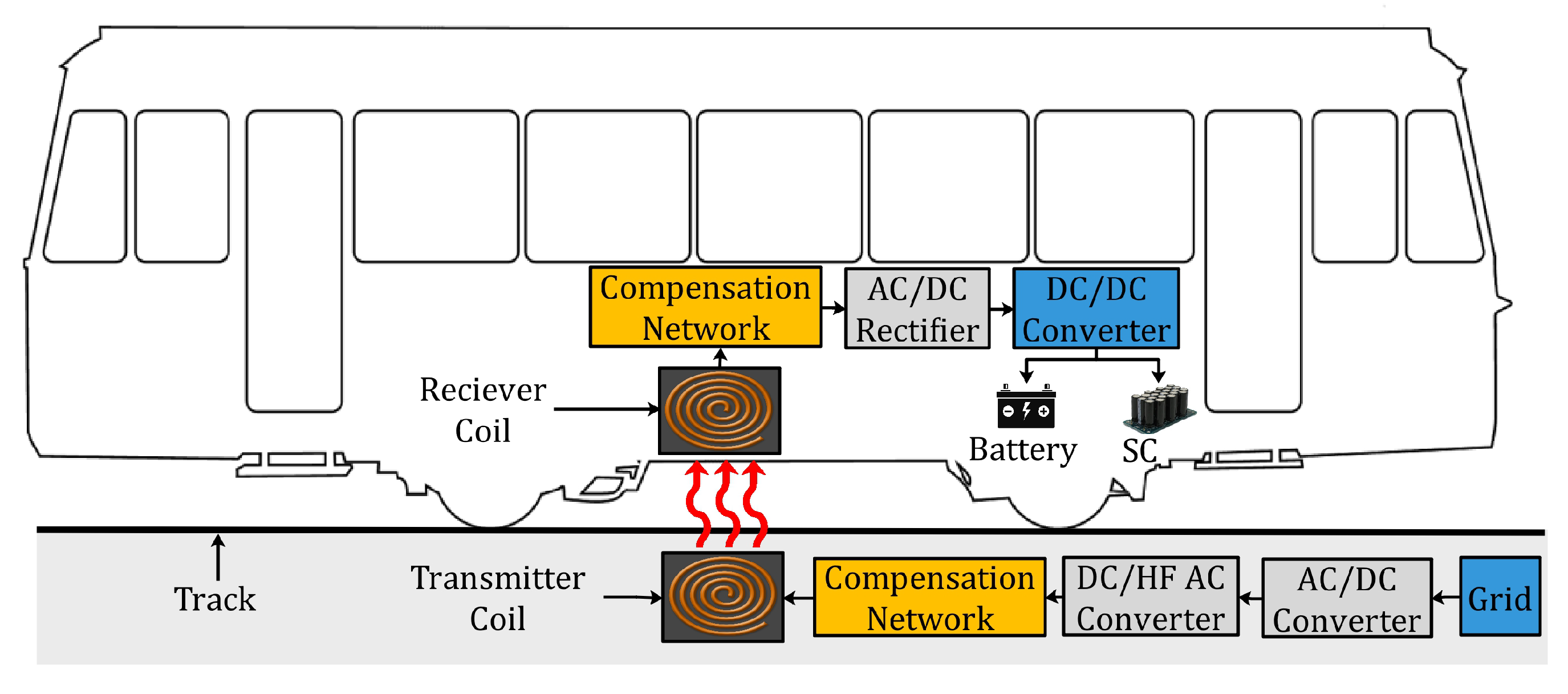
13]. A typical WPT–HESS system implemented in an LRV is shown in Figure 1.
On the transmitting side, a high frequency (HF) DC/AC inverter converts the DC power into the required HF AC power. The AC/DC rectifier on the receiving side converts the AC voltage back into DC voltage. The compensation networks are implemented on both sides to improve the system efficiency by canceling the leakage inductance and lowering the reactive power transfer [14,15]. Finally, the DC–DC converters are interfaced between the rectifier and storage units to control the power flow. Based on this topology, different attempts have been made to integrate an HESS with WPT. In [8], the author proposed a WPT–HESS system to charge an electric scooter. According to the battery state of charge (SOC), a three-mode strategy is proposed to meet the power demands of the battery and SC. In [16], an HESS-based WPT system was proposed in which the ESUs—i.e., the battery and SC—were linked to the WPT system by the DC–DC converter, and the implemented WPT system ensured a stable current to these units. The issue with such a configuration is that the power-receiving ability of the SC is wasted. In [17]; using the same HESS topology, the WPT and HESS system were configured to meet the desired power requirements of the storage devices. However, the article lacks an analysis of the WPT system efficiency, which is a key factor in designing a WPT system.
For the accurate charging of the battery and SC, a stable bus voltage is required. Therefore, the connected WPT system must provide a constant DC bus voltage to the ESUs. To solve this issue, the compensation networks that defines the system transfer characteristics—i.e., a constant current or constant voltage—are utilized [18]. Based on the inductor–capacitor structure, the compensation networks can be categorized as parallel–series, parallel–parallel, series–parallel and series–series [18]. The circuit diagrams of these networks are shown in Figure 2. In parallel–series and parallel–parallel configurations, the source is protected, since there is no power flow from the transmitter coil in the case of the non-availability of the receiver coil. The drawback of these networks is that if the transmitting and receiving coils are misaligned, then high power cannot be transferred [19]. To solve this problem, the series–parallel network can transfer high power, but its dependence on load variation and high voltage gain make its implementation limited [20]. The series–series network is widely used because, using this network, the resonant frequency does not vary with coupling-coefficient and load variations. The drawback of this network is that the output current and duty cycle of the connected DC–DC converter are inversely related, making the use of traditional control methods obsolete [21]. To solve this issue, an LCC-S-based WPT is proposed in [22] that can maintain a quasi-constant voltage at the output.
Another design element that needs consideration is the system efficiency of WPT and its dependence on the connected load; i.e., the WPT system provides maximum efficiency for a specific load. To operate the WPT system at this maximum efficiency point and control the power flow to the storage devices, DC–DC converters are interfaced between the WPT system and the connected ESUs [23]. By controlling the DC–DC converter duty cycle, the WPT system equivalent resistance can be altered; i.e., the duty cycle of buck and boost converters can change their input resistance in the range R L + and 0 R L , respectively [24]. Conventionally, the PID controller is implemented to control the duty cycle [25,26]. However, the linear nature of THE PID limits its regulation to a smaller region. A linear model predictive controller (MPC) is designed for a dynamic WPT system in [27] to control its output voltage. Compared to the PID controller, its response time is faster and it provides better system efficiency. However, the MPC controller needs an accurate dynamic model and an optimization algorithm, which implies high computation cost [28,29]. To expand the regulation range of the linear controllers, an SMC is presented in [30]. Due to its non-linear nature, the SMC not only exhibits faster tracking for different load conditions but also fewer transients. However, the SMC has some of its own shortcomings, such as overshooting and the presence of chattering at the equilibrium point. A high-order SMC based on a super-twisting differentiator is proposed in [31], enhancing the traditional SMC for a quick transient response. However, the gains of this improved controller should be optimized for various output voltages for a faster response time.
According to the above-mentioned literature, a WPT–HESS system based on the LCC-S compensation topology is presented in this article. The SC and battery are linked to the WPT system by buck and bidirectional buck–boost converters, respectively. To control the converter duty cycles, an integral terminal sliding mode controller (ITSMC) is proposed to overcome the drawbacks of the traditional SMC. Due to LCC-S compensation, the WPT system ensures stable output voltage at the DC bus. Furthermore, to ensure that the WPT system operates at maximum efficiency, the DC–DC converters are controlled to provide optimal power to ESUs. The ITSMC controls the connected bidirectional buck–boost converters to distribute the power flow between the ESUs and ensure that the WPT system provides the injected power at maximum efficiency. In the proposed WPT–HESS system, SC is considered as the main ESU and the battery as an auxiliary ESU. Therefore, the majority of the power is injected into the SC and the remaining power into the battery so that the injected power is equal to the optimal power. During the charging process, the voltage of the SC will rise, due to which its power requirement will increase. When the power requirement increases beyond a threshold, then the power generated from the WPT system will not be optimal; therefore, the battery will be discharged to make sure that the power generated from the WPT system is equal to the optimal power. A detailed energy management system (EMS) is devised to provide the current references for the charging of ESUs, and then the ITSMC is used to track the ESU’s charging currents to the desired references.
The article is structured as follows. The proposed WPT–HESS system and the connected DC–DC converters are modeled in Section 2. The EMS for the generation of the current references is discussed in Section 3. The design and closed-loop stability analysis of the proposed controller are discussed in Section 4. Section 5 presents the simulation results of the proposed WPT–HESS structure, comparison of the ITSMC with the PID and SMC and the validation of the simulation results by controller hardware in loop (C-HIL) experiments. Section 6 concludes the article.

2. System Modeling

2.1. Governing Equations of the LCC-S Compensation Network

Figure 3 shows the circuit diagram of the proposed WPT–HESS system using the LCC-S compensation network.
In the figure, L t and L r are the inductances of the transmitting and receiving coils and C t , C r are their series capacitors, respectively. L f 1 and C f 1 is the inductance of the compensation inductor and its compensation capacitor, respectively. R f 1 , R t and R r are the equivalent series resistances (ESRs) of L f 1 , L t and L r , respectively. V A B is the HF root mean square (RMS) AC voltage generated by the HF inverter from the input DC source V i n at resonant frequency ω . V a b is the HF AC voltage received at the receiving coil. V s c and V b a t are the DC voltages of the SC and battery, respectively. M is the mutual inductance between the transmitting and receiving coils. S 5 , S 6 and S 7 are the IGBT switches of the bi-directional buck–boost and buck converters connected with the battery and SC, respectively. L s c and L b a t are the inductors of the buck and bi-directional buck–boost converters, respectively. R b a t and R s c are the equivalent resistances of the battery and SC, which vary with their state of charge (SOC).
Figure 4a shows the equivalent circuit diagram of the proposed structure. The equivalent resistance R e q of the DC–DC converters connected with the battery and SC is derived by considering three different modes of the charging process. In all the three cases, the SC is charged through the connected buck converter; depending on the system requirements, the battery will either charge, not charge or discharge. In first mode—i.e., no battery mode—the DC–DC converter connected with the battery will not function, and therefore no charging or discharging occurs. In second mode—i.e., battery charging—the bi-directional DC–DC converter operates in buck mode to charge the battery. In the third mode, the bi-directional DC–DC converter operates in boost mode to discharge the battery. Based on these modes, V b a t can be derived as follows:
V b a t = 0 ( No battery ) μ 5 V C o ( Battery charging ) 1 μ 5 V C o ( Battery discharging )
Utilizing Equation (1), the equivalent resistance of the DC–DC converters in each mode can be derived as follows [24],
R e q = 8 π 2 R s c μ 7 2 ( No battery ) 8 π 2 R s c μ 7 2 | | R b a t μ 5 2 ( Battery charging ) 8 π 2 R s c μ 7 2 | | R b a t 1 μ 5 2 ( Battery discharging )
where ( 0 < μ 5 , μ 6 , μ 7 < 1 ) are the duty cycles of switches S 5 , S 6 and S 7 , respectively. Simplifying Equation (2), the equivalent resistance for all the three modes is derived as
R e q = 8 π 2 R s c μ 7 2 ( No battery ) 8 π 2 R b a t R s c μ 7 2 R b a t + μ 5 2 R s c ( Battery charging ) 8 π 2 R b a t R s c μ 7 2 R b a t + 1 μ 5 2 R s c ( Battery discharging )
The equivalent circuit is converted into a voltage-driven two-port network by transferring the receiving-side impedance to the transmitting side. Figure 4b shows the converted equivalent circuit. The transferred impedance of the secondary side Z r can be obtained as follows:
Z r = ω 2 M 2 R e q + R r
Furthermore, the system’s parameters are tuned to satisfy the resonance condition and make the phase difference between the input voltage and current zero. The resonance equations for tuning the system parameters are
C f 1 = 1 ω 2 L f 1 C t = 1 ω 2 ( L t L f 1 ) C r = 1 ω 2 L r
According to the two-port network shown in Figure 4b, the terminal voltages and currents are related as follows [32]:
V A B V a b * = Z 11 Z 12 Z 21 Z 22 I L f 1 I t
where V a b * is the voltage across Z r , derived as
V a b * = Z r I t = ω 2 M 2 I t R r + R e q
The system’s open-circuit impedance parameters are evaluated by considering the two operational modes as shown in Figure 5a,b. In mode (i), the output port is open-circuited ( I t = 0 ), and in mode (ii), the input port is open-circuited ( I L f 1 = 0 ). Considering these two modes and Equation (5), the open-circuit impedance parameters are calculated as [33]
Z 11 = V A B I L f 1 | I t = 0 = j ω L f 1 1 ω C f 1 + R f 1 = R f 1 Z 21 = V a b * I L f 1 | I t = 0 = 1 j ω C f 1 = j ω L f 1 Z 22 = V a b * I t | I L f 1 = 0 = R t + j ω L 1 1 ω C f 1 1 ω C t = R t Z 12 = V A B I t | I L f 1 = 0 = 1 j ω C f 1 = j ω L f 1
The WPT system voltage gain G V o from transmitting coil input to the receiving coil output is derived as follows,
G V o = V a b V A B = V a b V a b * V a b * V A B
Furthermore, using two port network theory, the input-to-output voltage gain V a b * V A B can be calculated as [34]
V a b * V A B = Z 21 Z r Z 11 Z r + Z 22 Z 12 Z 21
Substituting values from Equation (8), we get
V a b * V A B = ω 3 L f 1 M 2 R r + R e q R f 1 ω 2 M 2 R e q + R r + R t + ω L f 1 2
Using the voltage divide rule in Figure 4a, the output voltage V a b can be obtained as
V a b = j ω M I t R r + R e q R e q
Substituting Equations (7), (10) and (12) into Equation (9), the WPT system voltage gain is derived as
G V o = ω 2 L f 1 M R e q R r + R e q R f 1 ω 2 M 2 R e q + R r + R t + ω L f 1 2
Similarly, using the characteristics equations of the two-port network theory [34], the network input current I L f 1 and output current I t can be calculated as
I L f 1 = V A B Z 22 + Z r Z 11 Z 22 + Z r Z 12 Z 21 = V A B R t R r + R t R e q + ω 2 M 2 R f 1 R t R r + R t R e q + ω 2 M 2 + ω L f 1 2 R r + R e q
I t = V A B Z 21 Z 11 Z 22 + Z r Z 12 Z 21 = V A B ω L f 1 ( R r + R e q ) R f 1 R t R r + R t R e q + ω 2 M 2 + ω L f 1 2 R r + R e q
Utilizing Equations (14) and (15), the current gain G I o can be calculated as [34]
G I o = I t I L f 1 = Z 21 Z r + Z 22 = ω L f 1 R r + R e q ω 2 M 2 + R t R r + R e q
Equation (15) can be utilized to yield the equation for the receiving coil current I r as
I r = ω 2 M L f 1 V A B R f 1 R t R r + R t R e q + ω 2 M 2 + ω L f 1 2 R r + R e q
Assuming that the system is satisfying the resonance conditions, and ignoring the losses incurred in the inverter, rectifier and DC–DC converters, the overall system efficiency ( η ) is derived as
η = V a b * I t V A B I L f 1 R e q R r + R e q = G V o G I o R e q R r + R e q
Substituting the values of G V o and G I o from Equations (13) and (16) in Equation (18), η can be derived as
η = ω 4 L f 1 2 M 2 R e q R f 1 ω 2 M 2 R r + R e q + R t + ω L f 1 2 ω 2 M 2 R r + R e q + R t R r + R e q 2
To calculate the optimal equivalent resistance R o p , η is differentiated with respect to R e q as follows:
η R e q = 0 R o p = R t R r R f 1 + R r ω L f 1 2 + R L f 1 ω 2 M 2 R t R r + ω 2 M 2 R t R t R L f 1 + ω L f 1 2
According to Equation (3), for varying R s c and R b a t , the duty cycles of the DC–DC converters u 5 , u 6 and u 7 can be used to regulate R e q = R o p to ensure that the system operates at maximum efficiency. The tracking of R e q to R o p is complex for the HESS; therefore, the R o p is translated into optimal power P o p to ease the control process.
Using Equation (13), the conversion of R o p into P o p is derived as
P o p = V a b 2 R o p = 1 R o p ω 2 L f 1 M R e q V A B R r + R e q R f 1 ω 2 M 2 R r + R e q + R t + ω L f 1 2 2
Using Equation (21) and the system specification given in Table 1, the relationship between η and P w p t is shown in Figure 6. It can be observed that at the P o p —i.e., 310 watts— η is highest. To converge P W P T to P o p , the duty cycles u 5 , u 6 and u 7 of DC–DC converters are altered. The modeling of these converters is provided in the next section.

2.2. Modeling of the DC–DC Converters

2.2.1. Bi-Directional Buck–Boost Converter (Battery)

The battery is linked to the WPT system through a two-switch bidirectional buck–boost converter as shown in Figure 3. This includes a high-frequency inductor L b a t with its ESR R L b a t and two IGBT switches S 5 and S 6 . The switching states of S 5 and S 6 are controlled by applying the required PWM signals u 5 and u 6 , respectively. Furthermore, the S 5 and S 6 operate reciprocally; i.e., when S 5 is on, then S 6 is off, and vice versa. Depending upon the switching states of these switches, the converter can operate in both buck and boost modes. The switching states for both operations are given below.
S 5 = on ; S 6 = off ( Boost Mode ) S 5 = off ; S 6 = on ( Buck Mode )
The switching states are further controlled by the battery reference current i b a t r e f ; i.e., in boost mode, the battery will discharge ( i b a t < 0 ), and in buck mode, the battery will be charged ( i b a t > 0 ). To ease the control process, a new parameter J is defined as follows:
J = 1 i b a t r e f < 0 ( Boost Mode ) 0 i b a t r e f > 0 ( Buck Mode )
During boost mode—i.e., J = 1 —using the Kirchhoff voltage law (KVL), the mathematical model can be derived as
d i b a t d t = V b a t L b a t + R L b a t L b a t i b a t + 1 u 5 V C o L b a t
i w p t 1 = 1 u 5 i b a t
where i w p t 1 is the current from the WPT system. Similarly, during buck operation, the mathematical model is developed as
d i b a t d t = V b a t L b a t + R L b a t L b a t i b a t + u 6 V C o L b a t
i w p t 1 = u 6 i b a t
To obtain a global model, a virtual control u 56 is defined as
u 56 = J 1 u 5 + 1 J u 6
Using Equation (28), both operational modes are combined into an overall model defined by the following equations:
d i b a t d t = V b a t L b a t + R L b a t L b a t i b a t + u 56 V C o L b a t
i w p t 1 = u 56 i b a t

2.2.2. Buck Converter (Supercapacitor)

The SC is also linked to the WPT system by a DC–DC buck converter. The mathematical model of the buck converter is derived as [23]
d i s c d t = V s c L s c + R L s c L s c i s c + u 7 V C o L s c
i w p t 2 = u 7 i s c

2.2.3. Global Modeling

Utilizing Equations (29) and (31), both DC–DC converters can be modeled as
d i b a t d t = V b a t L b a t + R L b a t L b a t i b a t + u 56 V C o L b a t
d i s c d t = V s c L s c + R L s c L s c i s c + u 7 V C o L s c
To simplify the control design, Equations (33) and (34) are utilized to averaged the model over one switching cycle [35],
d x 1 d t = V b a t L b a t + R L b a t L b a t x 1 + μ 56 V C o L b a t
d x 2 d t = V s c L s c + R L s c L s c x 2 + μ 7 V C o L s c
where x 1 is average battery current i b a t , x 2 is the average SC current i s c and μ 56 and μ 7 are the average values of PWM signals u 56 and u 7 , respectively. To generate the reference currents for i b a t and i s c , an energy management system is devised in the next section.

3. Energy Management System (EMS)

3.1. Power Distribution Strategy

To ensure that the WPT system operates at the maximum efficiency, its output power should be optimally distributed between the SC and battery. The generated power from the proposed WPT–HESS system, P w p t , can be calculated as
P w p t = P b a t + P s c
where P b a t and P s c are the power delivered to the battery and SC, respectively. The WPT system’s main goal is to satisfy the load power requirements—in this case, the power requirements of the SC. However, to ensure that the WPT system operates at maximum efficiency, the power generation from the WPT system should be equal to P o p . For this purpose, when P s c is lower than P o p , the extra power is utilized to charge the battery. Conversely, when P s c is higher than P o p , the battery is discharged to fulfill the power demand of SC. Based on these charging conditions, the following power distribution rules are devised:
  • The SC should be charged to its rated power;
  • The WPT system should operate at maximum efficiency;
  • The charging time should be fully used to adequately allocate the charging power for the battery.
The power distribution between the HESS and WPT system is allocated based on the SC’s initial voltage level V s c i . Based on V s c i level, the SC is charged in two different modes, as shown in Figure 7. In the first case, when V s c i = V s c m i n , constant current charging is applied to ensure that the SC is charged to the rated power. Figure 7a shows the charging curves for this scenario. It can be seen that, due to constant current charging, P s c increases linearly with the rated power of SC.
The whole charging process is divided into three time periods. In period 1, the charging of SC begins with its lowest initial voltage, due to which the charging requirement of the SC is lower; therefore, the remaining power ( P w p t P s c ) is used to charge the battery. It can be observed that until P s c reaches P L = P o p P b a t m a x , the power from the WPT is not optimal, which shows that P L is the minimum threshold power in order to generate the optimal power generation from the WPT system. In period 2, with the increment in the charging requirement of the SC, the battery charging power P b a t starts to decrease to accommodate the SC charging requirements. It can be seen in period 3 that when P s c exceeds P o p , the battery is used as a power supply for the SC to meet its extra power requirements and to ensure that the power from the WPT system is optimal; i.e., P w p t = P o p . The P b a t and I b a t is negative in this period, which shows this discharging phenomenon.
The second scenario, in which the SC’s initial voltage is greater than the minimum voltage—i.e., V s c i > V s c m i n —is shown in Figure 7b. The charging process for this case is categorized into two stages. The first stage is demonstrated in period 1, in which a constant current is injected into the SC until its power reaches the turning power P t . Then, in the second stage, the charging is done by providing a constant power P t to fully charge the SC in the rated time T r .

3.2. Design of System Parameters

The maximum power level of the WPT system P w p t m a x in the proposed HESS structure is determined according to the power requirement of the attached SC and battery. The relationship between the WPT system and HESS units are as follows:
P w p t m a x P s c m a x P b a t m a x
where P s c m a x and P b a t m a x are the maximum power requirements of the SC and battery, respectively. Furthermore, when V s c i = V s c m i n , the battery power level must not be reduced during the charging process. To ensure this, the following relationship between P w p t m a x and P s c must hold.
P w p t m a x P s c m a x + P s c m i n 2
Based on the relationships given by Equations (38) and (39), P w p t m a x is selected as
P w p t m a x = max P s c m a x P b a t m a x , P s c m a x + P s c m i n 2
To generate P w p t m a x at maximum efficiency, the system parameters are tailored according to Equation (21). The charging process begins with the detection of V s c i . For V s c i = V s c m i n , a constant current mode will be applied, and for V s c i > V s c m i n , the first current mode and then constant power mode are applied. Figure 7b shows that, in the second stage, the charging of SC is done by constant power P t . This turning power for the SC is calculated as
P t = I s c m a x 2 T r + C I s c m a x V s c i I s c m a x I s c m a x T r + C V s c i 2 C V s c m a x 2 C
According to Equation (41), P t depends upon the level of V s c i . However, for a particular V s c i level, if P t is less than P L , then P t must be equal to P L to realize optimal power generation from the WPT system. In this case, the charging process will be completed quicker than the rated time. Based on these scenarios, the turning power can be chosen as
P t * = max P t , P L
The primary goal is to fully charge the SC; therefore, the battery charging power depends upon the remaining power from the rated power. This charging strategy is summarized as follows:
P b a t * = min P b a t m a x , P o p P s c
Utilizing Equation (43), it can be deduced that when P s c > P o p , then P b a t * will be negative, which validates the discharging phenomenon shown in period 3 of Figure 7a. All of the above-mentioned charging rules are summarized in a flowchart shown in Figure 8.
According to the power allocation strategy, it can be observed in Figure 8 that the current references I s c r e f and I b a t r e f are generated for the battery and SC charging, respectively. By tracking I s c to I s c r e f and I b a t to I b a t r e f , the WPT system will operate at maximum efficiency point under different V s c i levels. In order to track these currents, an integral terminal sliding mode controller is designed in the next section.

4. Designing of Integral Terminal Sliding Mode Controller (ITSMC)

An overall structure of the implemented control strategy is shown in Figure 9. A centralized ITSMC is proposed in this article, with the main motive of ensuring that the WPT system operates at the optimal power point. To accomplish this task, the ITSMC tracks the SC current i s c and battery current i b a t to their respective reference currents—i.e., i s c r e f and i b a t r e f —which are generated by the proposed EMS. To track i s c and i b a t to their referenced values, error trajectories are defined for each parameter as follows:
e 1 = x 1 i b a t r e f
e 2 = x 2 i s c r e f
where the errors e 1 and e 2 are used for the regulation of i b a t and i s c , respectively. Taking the time derivative of Equations (44) and (45) and using x ˙ 1 and x ˙ 2 from Equations (35) and (36), we get
e ˙ 1 = V b a t L b a t + R L b a t L b a t x 1 + μ 56 V C o L b a t i ˙ b a t r e f
e ˙ 2 = V s c L s c + R L s c L s c x 2 + μ 7 V C o L s c i ˙ s c r e f
To make the error signals equal to zero, the integral terminal sliding mode surfaces S 1 and S 2 are defined as
S 1 = e 1 + ζ 1 0 t e 1 d t λ 1
S 2 = e 2 + ζ 2 0 t e 2 d t λ 2
where ζ i and λ i are the design parameters of the ITSMC controller, defined as
ζ i > 0 i = 1 , 2 1 < λ i < 2 i = 1 , 2
The integrals of the error signals in the sliding surfaces improve the controller chattering and its dynamic system response for sudden changes in the parameters. Taking the time derivative of these sliding surfaces gives us
S 1 ˙ = e 1 ˙ + ζ 1 e 1 λ 1 0 t e 1 d t λ 1 1
S 2 ˙ = e 2 ˙ + ζ 2 e 2 λ 2 0 t e 2 d t λ 2 1
Taking the value of e 1 ˙ and e 2 ˙ from Equations (46) and (47) yields
S 1 ˙ = ζ 1 e 1 λ 1 0 t e 1 d t λ 1 1 + μ 56 V C o L b a t V b a t L b a t + R L b a t L b a t x 1 i ˙ b a t r e f
S 2 ˙ = ζ 2 e 2 λ 2 0 t e 2 d t λ 2 1 + μ 7 V C o L s c V s c L s c + R L s c L s c x 2 i ˙ s c r e f
To verify the stability of the proposed controller, a positive definite Lyapunov candidate function V is defined as follows:
V = 1 2 S 1 2 + 1 2 S 2 2
For asymptotic stability, the time derivative of V—i.e., V ˙ —must be negative semi-definite, derived as
V ˙ = S 1 S ˙ 1 + S 2 S ˙ 2
To make the V ˙ negative semi-definite, the following condition must be satisfied for S ˙ i :
S i ˙ = ψ i s g n ( S i ) , i = 1 , 2
where ψ i is the controller gain used to converge the states towards the sliding surface; i.e., the higher its value, the faster the converging speed and vice versa. Meanwhile, s g n is the signum function used to bind the states to remain on the sliding surface. Both of these controlling parameters are defined as
s g n ( x ) = x x x 0 0 x = 0
ψ i > 0 i = 1 , 2
Substituting the values of S ˙ 1 and S ˙ 2 from Equation (57) and into (56) yield
V ˙ = ψ 1 S 1 ψ 2 S 2
As ( ψ 1 , ψ 2 ) > 0, the V ˙ is negative semi-definite; therefore, the asymptotic convergence of the designed controller is verified by the Lyapunov stability criteria. Furthermore, the chosen sliding surfaces should also satisfy the existence condition, which is stated as follows:
S i S ˙ i < 0 i = 1 , 2 S ˙ i > 0 S i < 0 S ˙ i < 0 S i > 0
According to the existence condition presented in Equation (61), the surfaces can be derived as follows:
For ( S 1 , S 2 ) > 0 and ( μ 56 , μ 7 ) = 1, we get:
ζ 1 e 1 λ 1 0 t e 1 d t λ 1 1 + V C o L b a t V b a t L b a t + R L b a t L b a t x 1 i ˙ b a t r e f < 0
ζ 2 e 2 λ 2 0 t e 2 d t λ 2 1 + V C o L s c V s c L s c + R L s c L s c x 2 i ˙ s c r e f < 0
For ( S 1 , S 2 ) < 0 and ( μ 56 , μ 7 ) = 0, we get
ζ 1 e 1 λ 1 0 t e 1 d t λ 1 1 V b a t L b a t + R L b a t L b a t x 1 i ˙ b a t r e f > 0
ζ 2 e 2 λ 2 0 t e 2 d t λ 2 1 V s c L s c + R L s c L s c x 2 i ˙ s c r e f > 0
Satisfying the necessary condition of Equations (62)–(65), the control laws μ 56 and μ 7 are obtained as follows:
μ 56 = L b a t V C o ζ 1 e 1 λ 1 0 t e 1 d t λ 1 1 + ψ 1 s g n ( S 1 ) L b a t V C o R L b a t L b a t x 1 V b a t L b a t i ˙ b a t r e f
μ 7 = L s c V C o ζ 2 e 2 λ 2 0 t e 2 d t λ 2 1 + ψ 2 s g n ( S 2 ) L s c V C o V s c L s c + R L s c L s c x 2 i ˙ s c r e f
where μ 56 , and μ 7 are the duty cycles of the converters linked to the battery and SC, respectively. The boundary conditions for these control signals are defined as 0 < μ 56 < 1 and 0 < μ 7 < 1 . Furthermore, based on the referenced current value, the control input μ 56 is split before feeding into the PWM of the respective switches. Utilizing μ 56 and i b a t r e f , the generation of μ 5 and μ 6 is shown in Figure 9.

5. Results and Discussion

The performance of the ITSMC was verified by simulating the proposed WPT–HESS system for different V s c i levels in the MATLAB/Simulink platform. The uncontrolled rectifier was interfaced with the battery and SC through the DC–DC converters controlled by the ITSMC. The references for I b a t and I s c were generated for different V s c i levels from EMS, and then the ITSMC was used to track these currents to their required references; i.e., I s c r e f and I b a t r e f . The parameter of the WPT system and the compensation network were designed and are listed in Table 1. The specifications of the HESS system are listed in Table 2, and the components of the DC–DC converters and ITSMC are shown in Table 3. The nomenclature used in this manuscript is listed in Abbreviations.
To validate the proposed controller and power allocation strategy, the charging of SC was initialized with four different voltage levels; i.e., 5, 12, 22, and 35 V. The reference currents for these different levels of V s c i were generated by the EMS and then tracked by the proposed ITSMC.
In the first scenario, the charging began with the lowest V s c i level—i.e., 5 V—as shown in Figure 10a. It can be deduced that the SC was charged to its rated voltage—i.e., 50 V—in the required time of 45 s, satisfying rule 1. According to the power allocation strategy, the ITSMC tracked I s c to I s c m a x of 10 A for the whole charging process; i.e., the charging was done with a constant current. Observing the I b a t , it can be seen that initially, when the charging requirement of the SC was lower, the ITSMC charged the battery with the maximum current by tracking I b a t to I b a t m a x of 3.5 A. However, the I b a t gradually decreased due to the increment in the charging requirement of the SC. Furthermore, when the charging requirements of SC exceeded the optimal power of the WPT, the bidirectional buck–boost converter operated in boost mode to discharge the battery and, together with WPT, catered for the charging requirements. This discharging phenomenon can be observed at approximately 25 s as the I b a t was negative afterward. The power curves of this charging cycle are shown in Figure 10b. It can be realized from the mentioned Figure that the SC charging power P s c increased linearly to its maximum value of 500 W. Furthermore, when the P s c exceeded the P o p , the P b a t was negative afterward, showing the discharging of the battery to the SC, realizing rule 2. Observing the WPT power curve P w p t , it can be deduced that until the P s c reached P L , the P w p t was not optimal, but afterwards for the remaining charging process, the P w p t was at its optimal value of 310 W, satisfying rule 3.
In the next scenario, the initial voltage of the SC was increased to 12 V, i.e., V s c i = 12 V. Utilizing Equation (41), the turning power was calculated to be 296 W; therefore, according to the power allocation strategy, a two-step charging mode was used; i.e., the initial charging of SC by a constant current and then constant power. This charging phenomenon is shown in Figure 11a,b. It can be seen that until 17 s, the SC was charged by a constant current of 10 A until its power reached the turning power point; i.e., 296 watts. Afterward, the SC was charged with a constant power of 296 watts. Furthermore, the charging curves of ESUs and the WPT system shown in Figure 11a,b show that during the whole charging process, the battery charging power ensured that the WPT system generated the optimal power of 310 Watts.
When V s c i was increased to 22 V, using Equation (41), P t was calculated to be 224 W. Following the power allocation strategy, only the constant power mode was utilized to charge the SC. The remaining power from the WPT was used to charge the battery to ensure the optimal power generation from the WPT system. Figure 12a,b depicts this charging process.
Following the trend, when V s c i was equal to 35 V, the constant power mode was used again. The turning power P t for this V s c i was calculated as 175 W. However, in this scenario, the SC was fully charged in less time; i.e., 35 s. This charging process is shown in Figure 13a,b where it can be seen that the charging was completed quicker than the rated time of 45 s. To summarize all the scenarios, the turning power for each initial voltage is shown in Table 4.
To verify the performance of the ITSMC, Figure 14 shows the WPT system efficiency of the above four scenarios. Furthermore, the efficiency of non-HESS was also calculated by charging the SC from 5 to 50 V with a constant current of 10 A. The efficiency of the non-HESS is shown as V n o n H E S S . The efficiency in all of these cases was considered from the HF inverter input to the rectifier output. From Figure 14, it can be deduced that the ITSMC kept the proposed system at maximum efficiency; i.e., approximately 92%. It can also be observed that the efficiency of non-HESS depended upon the SC charging power P s c ; i.e., it increased until P o p and then decreased afterward.

5.1. Comparison with PID and SMC Techniques

To verify the robustness of the ITSMC and the previously used control techniques—i.e., PID and SMC—against the load variations, the connected load resistance R s c was abruptly varied with the perturbation frequency of 20 Hz; i.e., after every 0.05 s. Furthermore, fluctuations in the load were set at 40%. According to the mentioned perturbation conditions, the load was initially set at 5 Ω ; afterwards, it was incremented to 7 Ω and finally decremented to 5 Ω . The mentioned perturbation scheme can be defined as
R s c = 5 Ω , t 0 , 0.05   s , 7 Ω , t 0.05 , 0.1   s , 5 Ω , t 0.1 , 0.15   s .
Under the aforementioned load variations, the controllers were used to track a constant output current of 5 A. This regulation of the output current by the ITSMC, PID and SMC is shown in Figure 15. It can be seen that, compared to PID and SMC, the ITSMC tracked the current quicker with better accuracy. Under the perturbation at 0.05 s and 0.1 s, the ITSMC recovered much quicker compared to other controllers. Furthermore, the PID and SMC exhibited overshoots and a large settling time compared to the ITSMC.
To check the performance of the ITSMC, SMC and PID when tracking different current levels, the reference currents were abruptly varied after each 0.05 s. The variation in the reference current level with respect to time is shown below:
I s c r e f = 5 A , t 0 , 0.05   s , 4 A , t 0.05 , 0.1   s , 5 A , t 0.1 , 0.15   s .
The tracking of I s c for the above-mentioned perturbation in I s c r e f by ITSMC, SMC and PID is shown in Figure 16. It can be observed that, during the perturbations at 0.05 s and 0.1 s, compared to PID and SMC, the ITSMC tracked the reference current much quicker with no overshoot. The detailed comparison analysis of ITSMC with PID and SMC is listed in Table 5, consisting of the rise time, settling time, percentage overshoot and steady state error. It can be observed that the ITSMC outperformed PID and SMC in terms of robustness and less steady-state error, therefore reaching the maximum efficiency point in less time with greater accuracy [30].

5.2. Controller Hardware in Loop Results

To validate the simulation results, a controller hardware in loop (C-HIL) setup of the proposed WPT–HESS system for cost-effective real-time experiments is shown in Figure 17. For the C-HIL, MCU F28379D launchpads were utilized, comprised of TMS320F28379D dual core CPUs operating at 200 MHz. The launchpads were connected with a MATLAB embedded coder using Texas Instruments C2000 Delfino support library. The proposed WPT–HESS model which included a DC voltage source, HF inverter, compensation network, transmitting and receiving coils, power converters, a battery and an SC was modeled on MATLAB and translated into MCU F28379D launchpad 1 through the embedded coder. The proposed EMS and ITSMC control laws were implemented on MCU F28379D launchpad 2 with a switching frequency of 100 KHz. The PWM ports of launchpad 2 were linked with the GPIO ports of launchpad 1. Using the built-in analog-to-digital and digital-to-analog converters, a closed-loop system was formed. Utilizing the C-HIL setup, all the simulated scenarios were repeated and compared.
Figure 18a, Figure 19a, Figure 20a and Figure 21a shows the performance analysis of I s c , V s c , I b a t and V b a t for different V s c i levels. It can be seen in Figure 18a that when V s c i was initialized with 5 V, a constant value of 10 A was applied to fully charge the SC. Furthermore. when the P s c crossed over P o p , the battery was discharged to cater for the SC’s extra power. The second scenario for V s c i = 12 V is shown in Figure 19a. In this case, the segmented charging strategy—i.e., an initial constant current and then constant power—was applied. The third scenario shown in Figure 20a depicts the V s c i = 22 V in which constant power was applied to fully charge the SC. Finally, the last scenario is shown in Figure 21a, in which the SC was initialized with 35 V. In this case, again constant power was applied; however, the charging process was completed a little earlier. The power curves of the SC, battery and WPT system for all the mentioned scenarios are shown in Figure 18b, Figure 19b, Figure 20b and Figure 21b. It can be seen that for different levels of V s c i , the WPT system always generated P o p , thus ensuring operation at the maximum efficiency. Furthermore, it can be observed that, in all these scenario, the C-HIL results were consistent with the simulation results, validating the adequate performance of the ITSMC.

6. Conclusions

An LCC-S compensation network-based WPT–HESS system has been presented in this article. ESUs were connected with the WPT system using DC–DC converters which were controlled by the ITSMC to adjust the power flow between the ESUs and WPT system. The WPT system was analyzed by two-port network theory, and optimal efficiency equations have been calculated. Based on these equations, when the WPT system was linked with optimal load or generated optimal power, it operated at maximum efficiency. An EMS has been devised that generates the reference currents for the ESUs, ensuring the operation of WPT system at maximum efficiency and fully charging the SC. The duty cycle of the DC–DC converters was controlled by the ITSMC to track the currents of the ESUs to their respective references. The simulation results verified that, using the proposed EMS and ITSMC, the WPT system operated at its maximum efficiency point and the SC was charged to maximum capacity. A comparison with PID and SMC validated that the ITSMC tracked the reference current with less overshoot and a steady error. Real-time C-HIL experiments were conducted to further verify the performance of the ITSMC and indicated that the ITSMC ensured that the proposed WPT system always generated optimal power for different V s c i , thus ensuring operation at maximum efficiency.

Author Contributions

Conceptualization, N.A. and Z.L.; formal analysis, N.A. and Z.L.; funding acquisition, Z.L. and Y.H.; investigation, Z.L. and Y.H.; methodology, N.A., and H.A.; project administration, Z.L. and Y.H.; resources, Z.L. and Y.H.; software, N.A., Y.H. and H.A.; supervision, Z.L.; validation, N.A., Z.L., H.A. and I.A.; writing—original draft, N.A.; writing—review and editing, N.A., H.A. and I.A. All authors have read and agreed to the published version of the manuscript.

Funding

This research was funded by the Science and Technology Research Project of Shandong Province under Grant No. 2019GGX104080.

Institutional Review Board Statement

Not applicable.

Informed Consent Statement

Not applicable.

Data Availability Statement

Not applicable.

Conflicts of Interest

The authors declare no conflict of interest.

Abbreviations

The following abbreviations are used in this manuscript:
HFHigh frequency
EVsElectric vehicles
WPTWireless power transfer
AGVsAutomatic guided vehicles
LRVLight rail vehicles
PIDProportional–integral–derivative
ESUsEnergy storage units
SCSupercapacitor
EMSEnergy management system
C-HILController hardware-in-the-loop
SMCSliding mode controller
HESSHybrid energy storage system
SOCState of charge
LCCinductor-capacitor-capacitor
ITSMCIntegral terminal sliding mode controller
I b a t m a x Battery max current
C b a t Battery capacity
V s c m a x SC max voltage
V s c i SC initial voltage
V b a t , I b a t Battery voltage and current
V s c , I s c SC voltage and current
I s c m a x SC max current
C s c SC capacitance
V s c m i n SC minimum voltage
T r Total charging time
L b a t bi-directional buck-boost Inductor
L s c Buck converter Inductor
R b a t Battery resistance
R s c SC resistance
R L b a t ESR of L b a t
R L s c ESR of L s c
I s c r e f SC reference charging current
I b a t r e f Battery reference charging current
f c DC-DC Converter switching frequency
S 5 , S 6 , S 7 IGBT switches of buck and bi-directional buck-boost
μ 5 , μ 6 , μ 7 PWM signals of switches S 5 , S 6 and S 7
ψ 1 , ψ 2 ITSMC Controller gains
ζ 1 , ζ 2 , λ 1 , λ 2 ITSMC Controller gains
K p , K i , K d PID Controller gains
K 1 , K 2 SMC Controller gain
V i n Input voltage
L t Transmitting coil inductance
R t Transmitting coil resistance
L r Receiving coil inductance
R r Receiving coil resistance
MMutual inductance
f s WPT operating frequency
P W P T WPT Output power
L f 1 Transmitting side compation inductance
C f 1 Transmitting side parallel compensation capacitance
C t Transmitting side series compensation capacitance
R f 1 Transmitting side compensation inductor resistance
C r Receiving side series compensation capacitance
η WPT system efficiency
P w p t m a x WPT maximum power
P b a t Battery charging power
P s c SC charging power
P t Turning Power

References

  1. Lu, X.; Wang, P.; Niyato, D.; Kim, D.I.; Han, Z. Wireless Charging Technologies: Fundamentals, Standards, and Network Applications. IEEE Commun. Surv. Tutor. 2016, 18, 1413–1452. [Google Scholar] [CrossRef] [Green Version]
  2. Wireless Power Transfer for Smart Industrial and Home Applications. IEEE Trans. Ind. Electron. 2019, 66, 3959–3962. [CrossRef] [Green Version]
  3. Lu, X.; Niyato, D.; Wang, P.; Kim, D.I.; Han, Z. Wireless charger networking for mobile devices: Fundamentals, standards, and applications. IEEE Wirel. Commun. 2015, 22, 126–135. [Google Scholar] [CrossRef] [Green Version]
  4. Tang, Y.; Chen, Y.; Madawala, U.K.; Thrimawithana, D.J.; Ma, H. A new controller for bidirectional wireless power transfer systems. IEEE Trans. Power Electron. 2017, 33, 9076–9087. [Google Scholar] [CrossRef]
  5. Lu, F.; Zhang, H.; Mi, C. A two-plate capacitive wireless power transfer system for electric vehicle charging applications. IEEE Trans. Power Electron. 2017, 33, 964–969. [Google Scholar] [CrossRef]
  6. Gong, C.; Liu, D.; Miao, Z.; Wang, W.; Li, M. An NFC on two-coil WPT link for implantable biomedical sensors under ultra-weak coupling. Sensors 2017, 17, 1358. [Google Scholar] [CrossRef] [PubMed]
  7. RamRakhyani, A.K.; Mirabbasi, S.; Chiao, M. Design and optimization of resonance-based efficient wireless power delivery systems for biomedical implants. IEEE Trans. Biomed. Circuits Syst. 2010, 5, 48–63. [Google Scholar] [CrossRef]
  8. Hu, J.; Lu, F.; Zhu, C.; Cheng, C.; Chen, S.; Ren, T.; Mi, C.C. Hybrid Energy Storage System of an Electric Scooter Based on Wireless Power Transfer. IEEE Trans. Ind. Inform. 2018, 14, 4169–4178. [Google Scholar] [CrossRef]
  9. Yi, W.; Yuyu, G.; Zhongping, Y.; Fei, L. Parameter Optimization of Modern Tram Wireless Power Transfer Power Supply System. In Proceedings of the 2019 IEEE PELS Workshop on Emerging Technologies: Wireless Power Transfer (WoW), London, UK, 17–21 June 2019; pp. 49–52. [Google Scholar]
  10. Kongezos, V.K.; Allen, C.R. Wireless communication between AGVs (autonomous guided vehicles) and the industrial network CAN (controller area network). In Proceedings of the 2002 IEEE International Conference on Robotics and Automation (Cat. No. 02CH37292), Washington, DC, USA, 11–15 May 2002; Volume 1, pp. 434–437. [Google Scholar]
  11. Hao, Y.; Wang, J.; Liu, Y. Research on wireless power transfer system of automated guided vehicle based on magnetic coupling resonance. In Proceedings of the 2019 22nd International Conference on Electrical Machines and Systems (ICEMS), Harbin, China, 11–14 August 2019; pp. 1–4. [Google Scholar]
  12. Chen, W.; Liu, J.; Chen, S.; Zhang, L. Energy Shaping Control for Wireless Power Transfer System in Automatic Guided Vehicles. Energies 2020, 13, 2959. [Google Scholar] [CrossRef]
  13. Geng, Y.; Yang, Z.; Lin, F.; Wang, Y. Maximum power and efficiency transmission using parallel energy storage load for wireless power transfer systems. In Proceedings of the 2017 IEEE PELS Workshop on Emerging Technologies: Wireless Power Transfer (WoW), Chongqing, China, 20–22 May 2017; pp. 40–47. [Google Scholar]
  14. Li, S.; Mi, C.C. Wireless power transfer for electric vehicle applications. IEEE J. Emerg. Sel. Top. Power Electron. 2014, 3, 4–17. [Google Scholar]
  15. Qiu, C.; KT, C.; Ching, T.W.; Liu, C. Overview of wireless charging technologies for electric vehicles. J. Asian Electr. Veh. 2014, 12, 1679–1685. [Google Scholar] [CrossRef] [Green Version]
  16. Hata, K.; Huang, X.; Hori, Y. Notice of Removal: Power flow control of magnetic resonance wireless charing for hybrid energy storage system of electric vehicles application. In Proceedings of the 2015 54th Annual Conference of the Society of Instrument and Control Engineers of Japan (SICE), Hangzhou, China, 28–30 July 2015; pp. 1459–1462. [Google Scholar]
  17. Wang, L.; Gonder, J.; Burton, E.; Brooker, A.; Meintz, A.; Konan, A. A Cost Effectiveness Analysis of Quasi-Static Wireless Power Transfer for Plug-In Hybrid Electric Transit Buses. In Proceedings of the 2015 IEEE Vehicle Power and Propulsion Conference (VPPC), Montreal, QC, Canada, 19–22 October 2015; pp. 1–7. [Google Scholar]
  18. Wang, C.S.; Stielau, O.H.; Covic, G.A. Design considerations for a contactless electric vehicle battery charger. IEEE Trans. Ind. Electron. 2005, 52, 1308–1314. [Google Scholar] [CrossRef]
  19. Kalwar, K.A.; Mekhilef, S.; Seyedmahmoudian, M.; Horan, B. Coil design for high misalignment tolerant inductive power transfer system for EV charging. Energies 2016, 9, 937. [Google Scholar] [CrossRef] [Green Version]
  20. Cirimele, V.; Freschi, F.; Guglielmi, P. Wireless power transfer structure design for electric vehicle in charge while driving. In Proceedings of the 2014 International Conference on Electrical Machines (ICEM), Berlin, Germany, 2–5 September 2014; pp. 2461–2467. [Google Scholar]
  21. Spanik, P.; Frivaldsky, M.; Drgona, P.; Jaros, V. Analysis of proper configuration of wireless power transfer system for electric vehicle charging. In Proceedings of the 2016 ELEKTRO, Strbske Pleso, Slovakia, 16–18 May 2016; pp. 231–237. [Google Scholar]
  22. Geng, Y.; Li, B.; Yang, Z.; Lin, F.; Sun, H. A high efficiency charging strategy for a supercapacitor using a wireless power transfer system based on inductor/capacitor/capacitor (LCC) compensation topology. Energies 2017, 10, 135. [Google Scholar] [CrossRef]
  23. Ali, N.; Liu, Z.; Hou, Y.; Armghan, H.; Wei, X.; Armghan, A. LCC-S Based Discrete Fast Terminal Sliding Mode Controller for Efficient Charging through Wireless Power Transfer. Energies 2020, 13, 1370. [Google Scholar] [CrossRef] [Green Version]
  24. Li, Z.; Zhu, C.; Jiang, J.; Song, K.; Wei, G. A 3-kW wireless power transfer system for sightseeing car supercapacitor charge. IEEE Trans. Power Electron. 2016, 32, 3301–3316. [Google Scholar] [CrossRef]
  25. Li, H.; Li, J.; Wang, K.; Chen, W.; Yang, X. A maximum efficiency point tracking control scheme for wireless power transfer systems using magnetic resonant coupling. IEEE Trans. Power Electron. 2014, 30, 3998–4008. [Google Scholar] [CrossRef]
  26. Zhong, W.; Hui, S. Maximum energy efficiency tracking for wireless power transfer systems. IEEE Trans. Power Electron. 2014, 30, 4025–4034. [Google Scholar] [CrossRef] [Green Version]
  27. Zhou, Z.; Zhang, L.; Liu, Z.; Chen, Q.; Long, R.; Su, H. Model Predictive Control for the Receiving-Side DC–DC Converter of Dynamic Wireless Power Transfer. IEEE Trans. Power Electron. 2020, 35, 8985–8997. [Google Scholar] [CrossRef]
  28. Besselmann, T.; Lofberg, J.; Morari, M. Explicit MPC for LPV Systems: Stability and Optimality. IEEE Trans. Autom. Control 2012, 57, 2322–2332. [Google Scholar] [CrossRef] [Green Version]
  29. Zanon, M.; Gros, S.; Bemporad, A. Practical Reinforcement Learning of Stabilizing Economic MPC. In Proceedings of the 2019 18th European Control Conference (ECC), Naples, Italy, 25–28 June 2019; pp. 2258–2263. [Google Scholar]
  30. Yang, Y.; Zhong, W.; Kiratipongvoot, S.; Tan, S.C.; Hui, S.Y.R. Dynamic improvement of series–series compensated wireless power transfer systems using discrete sliding mode control. IEEE Trans. Power Electron. 2017, 33, 6351–6360. [Google Scholar] [CrossRef]
  31. Huangfu, Y.; Zhuo, S.; Rathore, A.K.; Breaz, E.; Nahid-Mobarakeh, B.; Gao, F. Super-twisting differentiator-based high order sliding mode voltage control design for DC-DC buck converters. Energies 2016, 9, 494. [Google Scholar] [CrossRef] [Green Version]
  32. Alexander, C.K.; Sadiku, M.N. Fundamentals of Electric Circuits; McGraw-Hill Education: New York, NY, USA, 2000. [Google Scholar]
  33. Sedra, A.S.; Sedra, D.E.A.S.; Smith, K.C.; Smith, K.C. Microelectronic Circuits; Oxford University Press: New York, NY, USA, 1998. [Google Scholar]
  34. Qiu, G.; Luo, X. Circuit; China Higher Education Press: Beijing, China, 2006; pp. 429–432. [Google Scholar]
  35. El Fadil, H.; Giri, F.; Guerrero, J.M.; Tahri, A. Modeling and nonlinear control of a fuel cell/supercapacitor hybrid energy storage system for electric vehicles. IEEE Trans. Veh. Technol. 2014, 63, 3011–3018. [Google Scholar] [CrossRef] [Green Version]
Figure 1. Wireless power transfer–hybrid energy storage system (WPT–HESS) implemented in a light rail vehicle (LRV).
Energies 14 01693 g001
Figure 2. Types of compensation networks: (a) series–series, (b) parallel–series, (c) series–parallel and (d) parallel–parallel.
Energies 14 01693 g002
Figure 3. Circuit diagram of the proposed WPT–HESS system.
Energies 14 01693 g003
Figure 4. (a) Equivalent diagram of the proposed system, (b) voltage-driven two–port network of the proposed system.
Energies 14 01693 g004
Figure 5. (a) Mode (i): I t = 0 (b) Mode (ii): I L f 1 = 0 .
Energies 14 01693 g005
Figure 6. Efficiency, η vs. R e q and P w p t .
Energies 14 01693 g006
Figure 7. Charging curves of HESS and WPT for (a) V s c i = V s c m i n (b) V s c i > V s c m i n .
Energies 14 01693 g007
Figure 8. Energy management system of the proposed WPT system.
Energies 14 01693 g008
Figure 9. General structure of the controlled system.
Energies 14 01693 g009
Figure 10. For V s c i = 5 V (a) V s c , I s c , V b a t , I b a t , (b) P s c , P b a t , P w p t .
Energies 14 01693 g010
Figure 11. For V s c i = 12 V (a) V s c , I s c , V b a t , I b a t , (b) P s c , P b a t , P w p t .
Energies 14 01693 g011
Figure 12. For V s c i = 22 V (a) V s c , I s c , V b a t , I b a t , (b) P s c , P b a t , P w p t .
Energies 14 01693 g012
Figure 13. For V s c i = 35 V (a) V s c , I s c , V b a t , I b a t , (b) P s c , P b a t , P w p t .
Energies 14 01693 g013
Figure 14. WPT system efficiency for different V s c i and V n o n H E S S .
Energies 14 01693 g014
Figure 15. Tracking of I s c , during perturbation in R s c .
Energies 14 01693 g015
Figure 16. Tracking of I s c , during perturbation in I s c r e f .
Energies 14 01693 g016
Figure 17. Configuration of the controller hardware in loop (C-HIL).
Energies 14 01693 g017
Figure 18. For V s c i = 5 V (a) V s c , I s c , V b a t and I b a t (b) P s c , P w p t , P b a t .
Energies 14 01693 g018
Figure 19. For V s c i = 12   V (a) V s c , I s c , V b a t and I b a t (b) P s c , P w p t , P b a t .
Energies 14 01693 g019
Figure 20. For V s c i = 22   V (a) V s c , I s c , V b a t and I b a t (b) P s c , P w p t , P b a t .
Energies 14 01693 g020
Figure 21. For V s c i = 35   V (a) V s c , I s c , V b a t and I b a t (b) P s c , P w p t , P b a t .
Energies 14 01693 g021
Table 1. Wireless charger parameters.
SymbolParameterValue
V i n Input voltage75 V
L t Transmitting coil inductance 167.7 μ H
R t Transmitting coil resistance∼190 m Ω
L r Receiving coil inductance 169.7 μ H
R r Receiving coil resistance∼270 m Ω
MMutual inductance 29.2 μ H
f s Switching frequency58 kHz
P W P T Output power310 W
L f 1 Transmitting side compensation inductance 33.4 μ H
C f 1 Transmitting side parallel compensation capacitance 0.25 μ F
C t Transmitting side series compensation capacitance 54.7 nF
R f 1 Transmitting side compensation inductor resistance100 m Ω
C r Receiving side series compensation capacitance 44.4 nF
Table 2. HESS specifications. SC: supercapacitor.
SymbolParameterValue
V b a t Battery voltage55 V
I b a t m a x Battery max current 3.5 A
C b a t Battery capacity 1.15 Ah
V s c m a x SC max voltage50 V
I s c m a x SC max current10 A
C s c SC capacitance10 F
V s c m i n SC minimum voltage5 V
T r Total charging time45 s
Table 3. Parameters of DC–DC converters and controllers. ESR: equivalent series resistance; ITSMC: integral terminal sliding mode controller; PID: proportional–integral–derivative; SMC: sliding mode controller.
SymbolParameterValue
L b a t , L s c Inductor 3.3 mH
R L b a t , R L s c ESR of inductor L b a t and L s c 20 m Ω
f c Converter switching frequency100 kHz
ψ 1 , ψ 2 ITSMC controller gains 20 , 000 , 20 , 000
ζ 1 , ζ 2 , λ 1 , λ 2 ITSMC Controller gains 0.3 , 0.3 , 1.5 , 1.5
K p , K i , K d PID controller gains 0.0825 , 24.05 , 6.548
K 1 , K 2 SMC gain 0.12 , 2.7
Table 4. Turning Power ( P t ) for different V s c i .
V s c i 5 V12 V22 V35 V
P t 500 W296 W224 W175 W
Table 5. Performance comparison between the PID, SMC and ITSMC.
Rise Time (ms)Settling Time (ms)Percentage Overshoot (%)Steady-State Error (%)
PID1.56515.18.10.21
SMC1.2835.411.120.2
ITSMC1.0643.5Nil0.006
Publisher’s Note: MDPI stays neutral with regard to jurisdictional claims in published maps and institutional affiliations.

