Abstract
In this paper, we demonstrate the high potentialities of pristine single-cation and mixed cation/anion perovskite solar cells (PSC) fabricated by sequential method deposition in p-i-n planar architecture (ITO/NiOX/Perovskite/PCBM/BCP/Ag) in ambient conditions. We applied the crystal engineering approach for perovskite deposition to control the quality and crystallinity of the light-harvesting film. The formation of a full converted and uniform perovskite absorber layer from poriferous pre-film on a planar hole transporting layer (HTL) is one of the crucial factors for the fabrication of high-performance PSCs. We show that the in-air sequential deposited MAPbI3-based PSCs on planar nickel oxide (NiOX) permitted to obtain a Power Conversion Efficiency (PCE) exceeding 14% while the (FA,MA,Cs)Pb(I,Br)3-based PSC achieved 15.6%. In this paper we also compared the influence of transporting layers on the cell performance by testing material depositions quantity and thickness (for hole transporting layer), and conditions of deposition processes (for electron transporting layer). Moreover, we optimized second step of perovskite deposition by varying the dipping time of substrates into the MA(I,Br) solution. We have shown that the layer by layer deposition of the NiOx is the key point to improve the efficiency for inverted perovskite solar cell out of glove-box using sequential deposition method, increasing the relative efficiency of +26% with respect to reference cells.
1. Introduction
Organic–inorganic hybrid perovskite cells (PSCs) are a new class of thin film photovoltaic (PV) devices promising to deliver efficient and cost effective solar energy to electricity conversion [1,2,3,4]. They are the hot topic in the field, because of their remarkable rise in power conversion efficiency (PCE) up to the current 25.5% record achieved for cell efficiency [5] and beyond 17% PCE of large area perovskite solar modules [6,7] PSC overcame the efficiency of other thin film PV technologies and the next target is matching the performance of crystalline silicon. Their success is certainly attributed to unique optoelectronic and semiconducting properties, which may be adjusted by varying the chemical composition of the material: tunable band gap, [8,9] large absorption coefficient (α = 5 × 103 cm−1 at 700 nm) [10], μm-range carrier diffusion length [11], ambipolar charge carrier transport [12,13], low density of trap states [14], and weak exciton binding energy [15]. Moreover, photoactive layers can be deposited using low-temperature and low-cost solution fabrication techniques, and scalable coating or printing methods allowing Roll-to-Roll (R-2-R) processing for flexible substrates [16,17,18]. There are many routes for the deposition and crystallization of the perovskite layers, such as solvent engineering [19,20,21], crystal engineering [22,23,24] co-evaporation and sequential evaporation [25,26,27], vapor-assisted solution process (VASP) [28,29], physical vapour deposition [30,31], and spray deposition [32]. Among them, the two-step perovskite formation or sequential deposition, originally introduced by Liang et al. [33] and then applied to PSCs by Burschka and co-workers [34], permits an easy deposition approach that could be conveniently used for large area devices [35]. In its original formulation for the deposition of CH3NH3PbI3 (MAPbI3), the two-step process involves first deposition of PbI2 on a substrate and a subsequent dipping in a CH3NH3I (MAI) bath. An optimized two-step deposition produces a high crystallinity of perovskite films (average grain size is more 200 nm), which helps to achieve films with reduced concentration of defects for high efficiency devices [23,24,36,37].
So far, the sequential deposition method was mainly used for n-i-p mesoporous structures and planar [22,24,37], where the perovskite is deposited on an electron transporting layer (ETL) porous scaffold, such as the meso-structured titanium dioxide (TiO2) and pure thin film of polyoxometalate [38]. This approach permitted to reach very efficient PSCs contributing to the development of the field [23]. However, the direct mesoscopic architecture has a few disadvantages that could compromise its exploitation for industrial applications, such as (i) strong hysteresis effect on the current–voltage (J–V) characteristics [39,40]; (ii) high-temperature process (480 °C) needed to sinter the mesoscopic TiO2; and (iii) the photocatalytic effects in the titanium dioxide upon ultraviolet (UV) illumination activate degradation processes in the perovskite [41,42]. The presence of hysteresis and the stability issue are also a bottleneck for the planar direct PSC where the mesoporous layer is replaced by a thin ETL such as SnO2 [43,44].
In order to eliminate the typical drawbacks of the n-i-p PSC architecture, inverted p-i-n planar structures have been proposed and developed with an increasing effort [45,46]. Here the perovskite is deposited on a hole transporting layer (HTL), which acts as window layer, oppositely to the n-i-p architecture where it is the back contact. The first material used for this application is PEDOT:PSS, a very versatile organic p-semiconductor widely employed in organic photovoltaics [47]. Another polymer, poly(triaryl-ammine) (PTAA), has proven to be a reliable material for reproducible high efficiency p-i-n perovskite solar cells [48]. Though efficiency, the liabilities of using organic materials are mostly related to their long time reliability in terms to environmental stability and UV induced degradation [49]. Nickel oxide (NiOX) is an inorganic stable material with a suitable HOMO level (in the range 5 to 5.6 eV according to the stoichiometry and synthesis) for hole extraction and injection and electron blocking properties in perovskite related applications [50]. Furthermore, NiOX can be deposited from liquid precursor in air [51,52,53] and annealed at the temperature below 300 °C [54]. Moving to the opposite side of the perovskite active layer, the typical ETL in solution-processed inverted PSCs is a fullerene derivative (PC61BM) that has the tendency to passivate perovskite surface with a significant suppression of hysteresis and recombination losses [55,56].
Despite the fact, that the sequential deposition of perovskite is well studied and described in the literature for conventional n-i-p structures [23], similar works for inverted planar structures with crystallization of perovskite on a p-type semiconductor surface has been discussed only in few publications and only for the pure MAPbI3 perovskite [57,58,59]. The first report of a sequential deposition of perovskite on NiOX on Indium tin oxide (ITO) was in 2014 by Hu et al., whose best optimal device structure with the reactive aluminium back electrode evaporated directly over the Phenyl-C61-butyric acid methyl ester (PCBM) yielded a PCE of 7.6% [58,60]. Even the performance were reported on poly(3,4-ethylenedioxythiophene) polystyrene sulfonate (PEDOT:PSS), where the sequential deposition could not yield performance above 2.6% for a 460 nm thick MAPbI3 layer, with efficiency dropping with increasing dipping time (hence, perovskite thickness). The authors attribute this to the penetration of 2-propanol (IPA) through PbI2, causing damage to the underlying PEDOT:PSS layer [59]. Recently, J. Duan et al. extended the two-step approach for inverted PSC to a two-cation perovskite FAMAPbI3 even though the low final efficiency (10.8%) does not allow to perform a clear assessment of the fabrication methodology.
This work is devoted to filling this gap, a required step considering the high potentialities of the multication perovskite combined with sequential deposition and inverted architecture for industrial exploitation of perovskite photovoltaic technologies. The reasons behind choosing the multication perovskite are its higher reproducibility and superior performance and stability [6,61,62]. The partial substitution of methylammonium with formamidinium helps the stability and the performance of the cells [63], while cesium addition stabilizes the crystal structure of the multication perovskite (single step or sequential deposition). The presence of bromine enlarges the band gap, making the material more versatile in terms of applications [22,64].
As a first step of our work, we have tried to apply the crystal engineering approach for pure MAPbI3 perovskite deposition following previous work reported in reference [23] and we have optimized the sequential deposition of the MAPbI3 perovskite layer on NiOX HTL reaching 14% efficiency under ambient conditions with relative humidity of 20 to 30%. Other interesting aspect is that the PCBM) and BCP (Bathocuproine) layers also were deposited by solution processes, fast and easy method to do while preventing any evaporation step at this stage. We also have compared the deposition of PCBM and BCP inside and outside of glove-box and interestingly there was only a ~9% lost in the efficiency applying PCBM/BCP out of glove-box, the result is presented in Figure S1 and Table S1 in Supporting Materials. In the second part of the work, mixed cation compositions [22] in air for inverted (p-i-n) planar solar cells were optimized. At first, we optimized the Pb(I,Br)2/CsI layer deposition by controlling of the pre-heating and sintering procedures to create smooth planar film. The second step included modification of dipping time of substrates into the MAX solution in anhydrous IPA and concentration of multication solution. The efficiency of 15.6% has been achieved, which is superior to previous works presented in the literature. Moreover, during the study, it was revealed that the critical parameters of the technological process are temperature control of the substrate, NiOX layer thickness, the multiple layer deposition of NiOX, PbX2 layer and timing for immersed substrates in MA(I,Br) in IPA solution during the second step of the deposition.
We should point out that PSCs were fabricated with solution processed PCBM and BCP layers from easy and fast approach that prevent the typical evaporation step. Moreover, all J–V measurement of PSCs were obtained in ambient conditions (relative humidity ≈50–60%), under solar simulator with 1 Sun showing hysteresis free plots with high value of current density comparable to meso-structure devices [39].
2. Materials and Methods
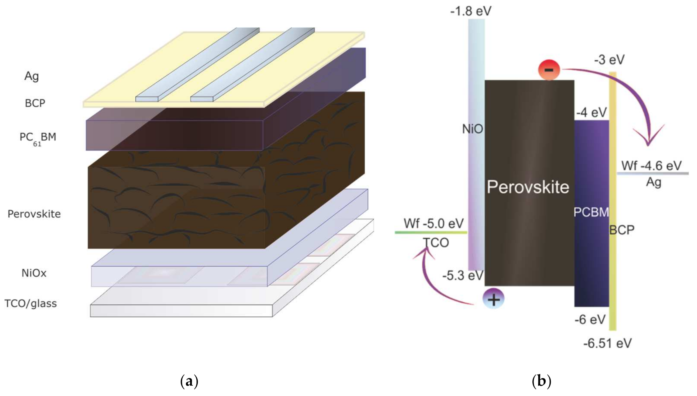
Inverted planar perovskite solar cells have been fabricated considering the glass/TCO/NiOX/Perovskite/PCBM/BCP/Ag stack (Figure 1a). Schematic of two-step perovskite formation on NiOX HTL is presented in (Figure 2).

Figure 1.
(a) Schematic representation of p-i-n perovskite solar cells (PSCs); (b) the related energy band diagram of the different functional layers relative to vacuum.
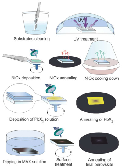
Figure 2.
Schematic representation of two-step perovskite formation on NiOX hole transporting layer (HTL).
2.1. Materials
ITO and fluorine doped tin oxide (FTO) substrates were purchased from Kintec and Pilkington, respectively. The solution of NiOx was obtained according to a previously reported recipe [53]. The other materials and solvents used are: 2-propanol (IPA, Sigma-Aldrich, anhydrous, 99.5%), lead iodide powder (PbI2, TCI, 99.99%), lead bromide powder (PbBr2, TCI, 99.99%), methylammonium bromide powder (CH3NH3Br, Dyesol), formamidinium iodide powder (CH3(NH2)2I, Dyesol), N,N-dimethylformamide (DMF, Sigma-Aldrich, anhydrous, 99.8%), cesium iodide (CsI, Puratrem), Dimethyl sulfoxide (DMSO, Sigma-Aldrich, anhydrous, St. Louis, MO, USA, 99.8%), [6,6]-Phenyl C61 butyric acid methyl ester powder (PC61BM, Solenne), bathocuproine (BCP, Sigma Aldrich, St. Louis, MO, USA, 99.99%).
2.2. Device Fabrication for MAPbI3 Perovskite
ITO/glass substrates (Kintec, 15 Ω cm−1, 25 mm × 25 mm) were patterned by a raster scanning laser (Nd:YVO4 pulsed at 80 kHz) to separate the active area of 4 pixels on each substrate. Cleaning process of glasses starts with mechanic washing in detergent water (Hellmanex 2% in deionized water) to exclude dusts and visible contaminations. Then substrates were rinsed in deionized (d/i) water, then ultra-sonicated (US) detergent water and then deionized water, acetone, and IPA for 3 min each step, respectively. Surface activation of substrates was carried out under ultraviolet (UV) lamp for 30 min before starting depositions of functional layers. Then, 30 nm NiOX hole-transporting layer was deposited on ITO following the procedure described in Ref. [53]: a NiOx precursor solution was spin-coated for 50 s at 3000 rpm with 3 s ramp and then annealed at 250 °C for several minutes to evaporate residual solvent it the deposition was repeated for 3 times and then at 300 °C for 60 min on hotplate with closed lid (to minimize influence from environmental fluctuations).
The sequential deposition method was used to fabricate perovskite films on the HTL and the procedure is represented in Figure 2. For the pure MAPbI3 perovskite following the idea of our previous work [23]. Firstly, 500 mg of PbI2 was dissolved in DMF while keeping for 20 min at 100 °C to dissolve completely and reaching clear solution and then decreasing the temperature to 70 °C, then 150 µL of solution was deposited on 45 °C NiOX substrate (substrate was kept under UV for 30 min and when the temperature reach to 40–45 °C we deposited PbI2 on the NiOx substrate with 5000 rpm for 10 s). PbI2-DMF layer was dipped in a solution of methylammonium iodide (CH3NH3I in anhydrous 2-propanol 10 mg mL–1) for 10 min at room temperature while the solution was kept in mechanical stirring during the dipping time. The surface treatment of the film immediately was done with 2-propanol via spin-coating at 6000 rpm with an acceleration rate of 6000 rpm for 10 s. Finally, the devices were annealed at 115 °C for 10 min. All the processes have been done out of glove-box. After that PC61BM in chlorobenzene, 20 mg mL−1 was deposited via spin-coating method a thin layer of ETL was made by 2 sequential steps of spin-coating at 500 rpm—1 s, 1500 rpm—30 s, and annealed at 50 °C for 5 min. Bathocuproine (BCP) in IPA (0.5 mg mL−1) was spin-coated as a thin buffer layer between PCBM and the Ag cathode. After electron conductor deposition, solar cells were completed by thermal evaporation (vacuum was 10−6 Torr) of 100 nm of Ag, which was deposited in at an initial slow rate of 0.3 Å/s for the first 10 nm, then 1 Å/s until the final thickness.
The best efficiency reached by this method out of glove-box is 14% which is still higher than the work has been published till now in the literature (maximum PCE of 7.6%).
2.3. Device Fabrication for Multication Perovskite
For multication perovskite deposition, firstly, 150 µL of mixed lead solution (Cs-Pb-I-Br) (PbI2/PbBr2/CsI(1.5 M stock solution of CsI in DMSO)(71:14:15 mol%) in DMF/DMSO (80:20 v%) heated at 70 °C with intensive stirring was dropped on pre-heated at 50 °C substrates and immediately spin-coated in ambient conditions with high relative humidity level (RH) about 50–60%. The solution was dropped by static dispense on the surface and spin-coated 10 s at 4000 rpm. After this procedure to improve material adhesion over the full surface and achieve porous layers, the substrates were sequentially heated at 40 °C for 2 min, then were dried in desiccator for 3 min. The second step consists of the dipping of the cooled-to-room-temperature layers in multication solution of FAI/MABr (88:12 mol%) in anhydrous 2-propanol with concentrations of 40 mM for 10, 20, 25, 30, 35, and 45 min to completely convert lead films into perovskite. In this dipping time the films turn from yellow color to dark brown/black. the best performance perovskite reaches by 30 min dipping in MAX solution. The final steps are surface treatment of the perovskite film with anhydrous 2-propanol pure solvent which deposited by spin-coating at 6000 rpm for 10 s and final annealing at 115 °C for 10 min. The full detailed procedure and method is reported in Ref. [23]. After perovskite full formation in air, the organic electron-transporting layer and a thin buffer layer and electron conductor were deposited as, mentioned above for MAPbI3. After metal cathode deposition by thermal evaporation, samples were removed from the vacuum chamber to dry in ambient conditions for oxygen saturation of samples for the next 4 h. It was noted that samples which were measured immediately showed lower performance than devices left settling in air. The picture of different layers is presented in the Supporting Materials Figures S2 and S3.
2.4. Device Measurement and Evaluation
Fabricated perovskite solar cells were measured using a solar simulator ABET Sun 2000, class A calibrated with certified Si cell and Ophir irradiance meter under AM 1.5 G and 100 mW∙cm−2 of illumination conditions in air with active area equals 0.16 cm2). Scan of J–V-parameters of devices were measured in both reverse (open-circuit voltage (Voc) to 0) and forward (0 to Voc) scan directions with 0.1 V step via a Keithley 2400 SMU controlled by a home-made Labview software. External quantum efficiency (EQE) EQE is based on a 300 W Xenon lamp and double grating (300 to 1400 nm). A correct integration of the incident monochromatic light was made by comparison with a photo-response of a Si UV-enhanced NIST calibrated photodetector, transient photocurrent (TPC) and Transient Photo Voltage (TPV) analysis of devices was performed with an ARKEO system from Cicci Research. In the TPV tests a high-speed LED based system (5000 Kelvin) is used to create small perturbation optical signals tuned to maintain voltage deflection within 50 mV. Steady state light was increased from 0.3 to 2 SUN equivalent Optical characterizations of films were executed with BLACK-Comet UV–VIS Spectrometer and ARKEO system. Morphological characterization of perovskite films was made with Profilometer and Scanning Electron Microscopy ZEISS. For the PL test the substrate is by a diode-pumped solid-state (DPSS) Nd:YVO4 + KTP Laser (Peak wavelength 532 nm ± 1 nm, Optical power 1 mW) at an inclination of 45° creating a circular spot 2 mm in diameter (31 mW/cm2) or with a collimated UV LED (Peak wavelength 380 nm ± 5 nm)
3. Results and Discussion
3.1. Absorbance + Photoluminescence (PL)
Absorbance spectra were measured on mixed cation/anion Cs-CH3NH3-CH3(NH2)2-Pb(I-Br)3 (here called multication) and pure MAPbI3 perovskite films fabricated by two-step method of fabrication inverted perovskite solar cells in ambient conditions. Figure 3a shows the UV–VIS absorption spectra of multication and pure MAPbI3 films. The absorbance spectrum of the multication shows an onset at 760 nm which is representing ~10 nm red shift with higher intensity compare to MAPbI3 absorbance spectrum. To prove the obtained current value, we measured absorbance for each multication perovskite films depending on dipping time (shown in Figure S4a). The PL measurements were performed on perovskite films with (multication or MAPbI3)/NiOX/FTO configuration. Figure 3b shows the normalized PL spectrum of both films. The PL peaks of the films for pure MAPbI3 and multication point at 764.2 nm and 782.5 nm, respectively. This confirms the different band-gaps of the two compositions, with MAPbI3 having a 1.56 eV energy gap and multication perovskite with a 1.63 eV band gap, as reported in the literature [22,64,65].
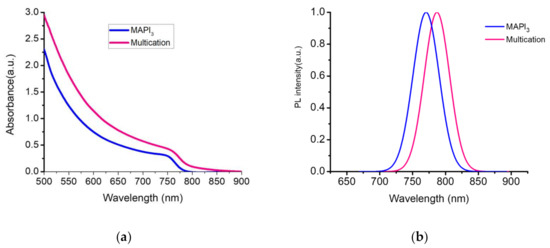
Figure 3.
(a) Absorbance spectra for multication and MAPbI3 perovskite films; (b) Photoluminescence (PL) of multication and MAPbI3 films on NiOX/FTO.
The PL measurements of multication perovskite films with different dipping time is reported in Figure S4b.
3.2. Subsection Perovskite Film Formation and Dipping Time
In order to achieve a higher efficiency of solar devices than previous reports [58], firstly, multication perovskite deposition has to be optimized by varying the dipping time for better coverage of the surface and, most of all, to increase the thickness of the absorber. We started to immerse our samples in mixed FA-MA cation solution for mixed cation/anion perovskite formation from 10 min and increased this time at 5 min-steps, reaching to 45 min. As a result, we measured dependence of short-circuit current density (JSC) and efficiency (PCE) on dipping time on one-layer NiOx that correspond to a thickness of around 8–10 nm. Statistic PV parameters were extracted from J–V plots and are presented in Figure S5b–e. As shown in Figure S5a, JSC increases until 30 min dip-coating and then decreases for longer dipping times.
Using a two-step method for inverted planar structure we achieved a higher JSC with respect to a single-step coating [66]. The single-step spin-coating method has a morphological limitation (lower grain size and reduced absorber thickness), while applying the two-step sequential technique leads to a more controlled crystallization of the perovskite film. The dependence of JSC on the dipping time could be explain this by two concurring causes. As the thickness increases (increasing dipping time), the charge carriers which are photo-generated away from the extraction layers will have to travel through a longer distance. If this distance is longer than the diffusion length, non-radiative recombination phenomena becomes important. This is also witnessed by the reduction of the open-circuit voltage (VOC) for dipping time longer than 30 min. At the same time, even though a thicker perovskite layer should result in improved light harvesting, the lower amount of collected charge carriers will result in a reduction JSC as observed for long dipping time. In addition, after an initial time in which most of the lead halide film is converted to perovskite, the IPA in the solvent starts dissolving the film and prolonged dipping time could result in a damage of the perovskite layer. As a result, efficiency drops, following the same trend of the current density.
Since amelioration of the perovskite film quality is one of the key parameters for highly efficient PSCs, we evaluated the effects of the annealing environment on initial PbX2/CsI film. Firstly, we attempted to get rid of the cloudy surface of the obtained film. Compared to 2 kinds of annealed on 40 °C and 50 °C lead iodide-bromide films, we found that on planar n-i-p structure less annealing temperature (40 °C) of PbX2/CsI layer leads to formation of pin hole-free, large crystals and clean-bright surface which is generally more suitable. Moreover, excess amount of PbX2 layer which is remained on the interface HTL/Perovskite has a positive effect deriving from the passivation of defects (at the interface and grain boundary), thus minimizing energy losses [67]. In addition, dip-coating of cold substrates in mixed cation solution promotes the fast growth of perovskite crystals by penetration of mixed cations through the PbX2/CsI layer. The nucleation process directly depends on dipping time, concentration of the solution, relative humidity and surface coverage. Larger perovskite crystals formation leads to high values of current density. The photocurrent density increases up to around 22 mA/cm2 confirming larger perovskite grains [68]. Wanyi Nie and co-workers explained that high value of PSC performance is due to an increased mobility and lower bulk defects (lower trap state density and reduced recombination centres) in large-size perovskite grains [69]. It meant that (i) micro-scale perovskite grains have low bulk defects and higher mobility of carriers, allowing for the unhampered migration and collection of charges; (ii) the reduced interfacial area associated with large grains suppresses charge trapping and eliminates hysteresis (irrespective of the direction of voltage sweep or the scan rate) [69].
In this respect, the lower Fill Factor (FF) exhibited by our devices is related more to the perovskite/NiOX interface, which will need to be optimized by surface modifications or doping of the hole selective layer to reduce the non-radiative recombination happening at that interface [56,70].
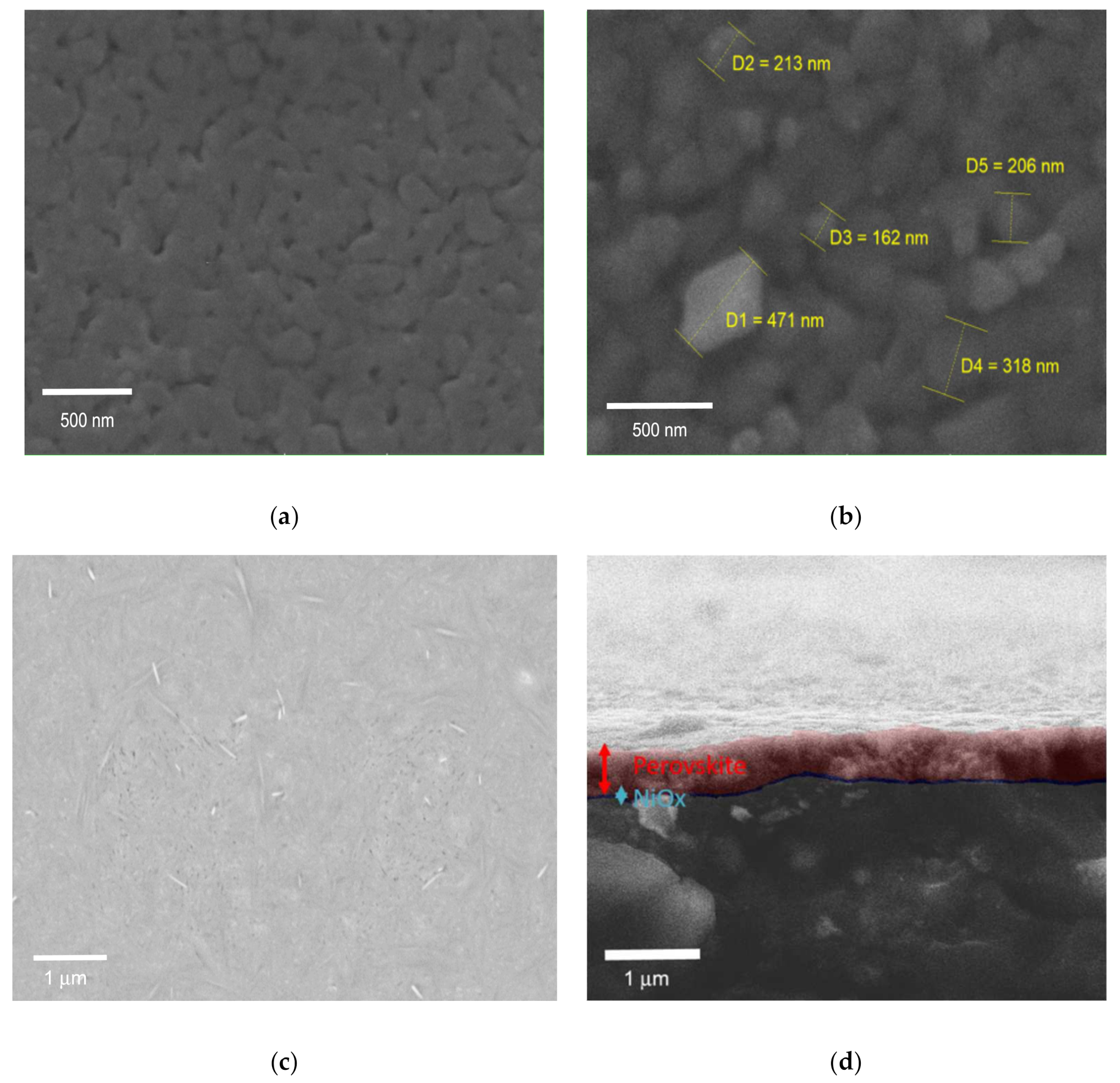
The above consideration on grain size is also supported by the morphological investigation of our sample performed via Scanning Electron Microscopy (SEM). Figure 4a,b shows the SEM image of PbI2 layer and MAPbI3 films, the PbI2 film appears to be smooth, but porous at the same time. The porosity of the spin-coated lead halide layer is conserved by the low temperature annealing ramp [23], in a similar manner to what happens for the fabrication of other porous films like in the mesoscopic perovskite solar cell structure. As it is shown in the Figure 4b the size of MAPbI3 grain is around 200 to 450 nm. Figure 4c shows the SEM image of FTO/NiOX/PbI2-PbBr2-CsI films after the first step of the CE method needed to prepare lead contained film. Figure 4d shows the SEM image of Glass-FTO/NiOX/multication perovskite film reaching around 500–550 nm thickness of perovskite layer. To confirm the obtained thickness results for perovskite layer and allow a direct comparison of the different absorber films and the corresponding dipping times, we measured by profilometry both kinds of perovskite compositions. Increasing the dipping time for both cases leads to the perovskite thickness rise.
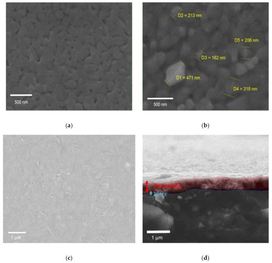
Figure 4.
(a) Scanning Electron Microscopy (SEM) image of the PbI2 film; (b) MAPbI3 perovskite film; (c) Pb(Br-I)2 film surface on NiOX/FTO; (d) Cross-section of multication perovskite film on NiOX/FTO.
3.3. Photovoltaic Performance
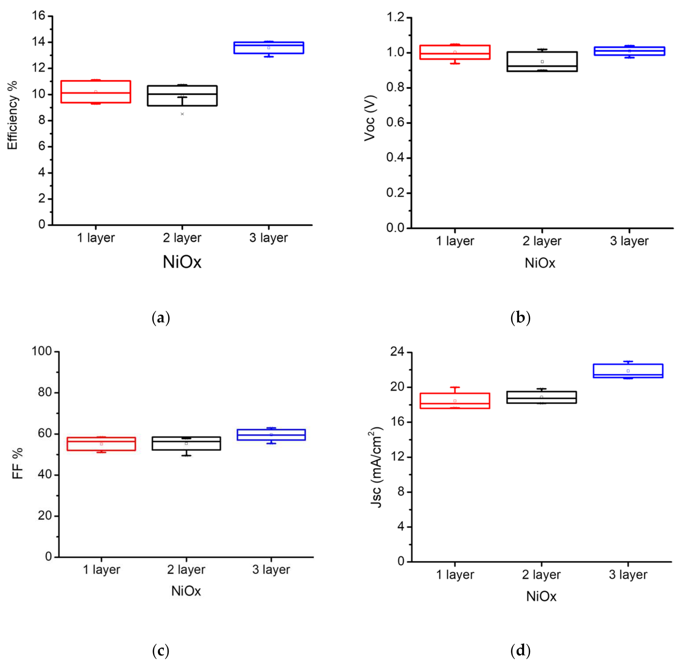
The statistic photovoltaic parameters of MAPbI3 on multiple layer NiOX and relation to the efficiency is presented in Figure 5 and Table 1. The results show that by increasing the thickness of NiOX through layer-by-layer deposition, Fill Factor and JSC and efficiency has been improved. Accordingly, we selected the three-layer deposited NiOx (~30 nm thickness) for all perovskite structures. Furthermore, photovoltaic parameters of best fabricated MAPbI3 and multication PSCs under 1 Sun (AM 1.5 G irradiance of 100 mW/cm2) are presented in Table 2, where the maximum efficiency for the champion multication PSC is higher than the best MAPbI3 PSC. A PCE of 15.63% (JSC = 21.92 mA/cm2, VOC = 1.04 V, FF = 68.75%) and 14% (JSC = 22.5 mA/cm2, a VOC = 1.00 V, and FF = 62.5%) were achieved for multication and MAPbI3 perovskite, respectively while all the deposition of the NiOx and perovskite layers and measurements were performed under ambient air conditions (out of glove-box). J–V curves of the champion multication and MAPbI3 PSCs are presented in Figure S6. On the other hand, we also tested the fully out of glove-box deposition (including the PCBM/BCP deposition) and the results just showed ~9% decay of the performance respect to inside glove-box deposition of PCBM/BCP layer (Figure S1 and Table S1).
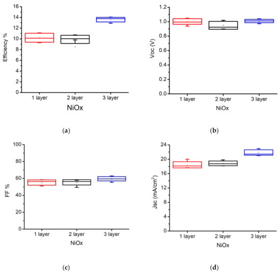
Figure 5.
Statistical photovoltaic parameters of the of MAPbI3 perovskite vs. multiple NiOX layer deposited: (a) Power Conversion Efficiency (PCE); (b) open-circuit voltage (VOC); (c) Fill Factor (FF); (d) short-circuit current density (JSC).

Table 1.
The best (average) photovoltaic parameters of the of MAPbI3 based PSCs for different layers of NiOX.

Table 2.
The best (average) photovoltaic parameters of optimized PSCs.
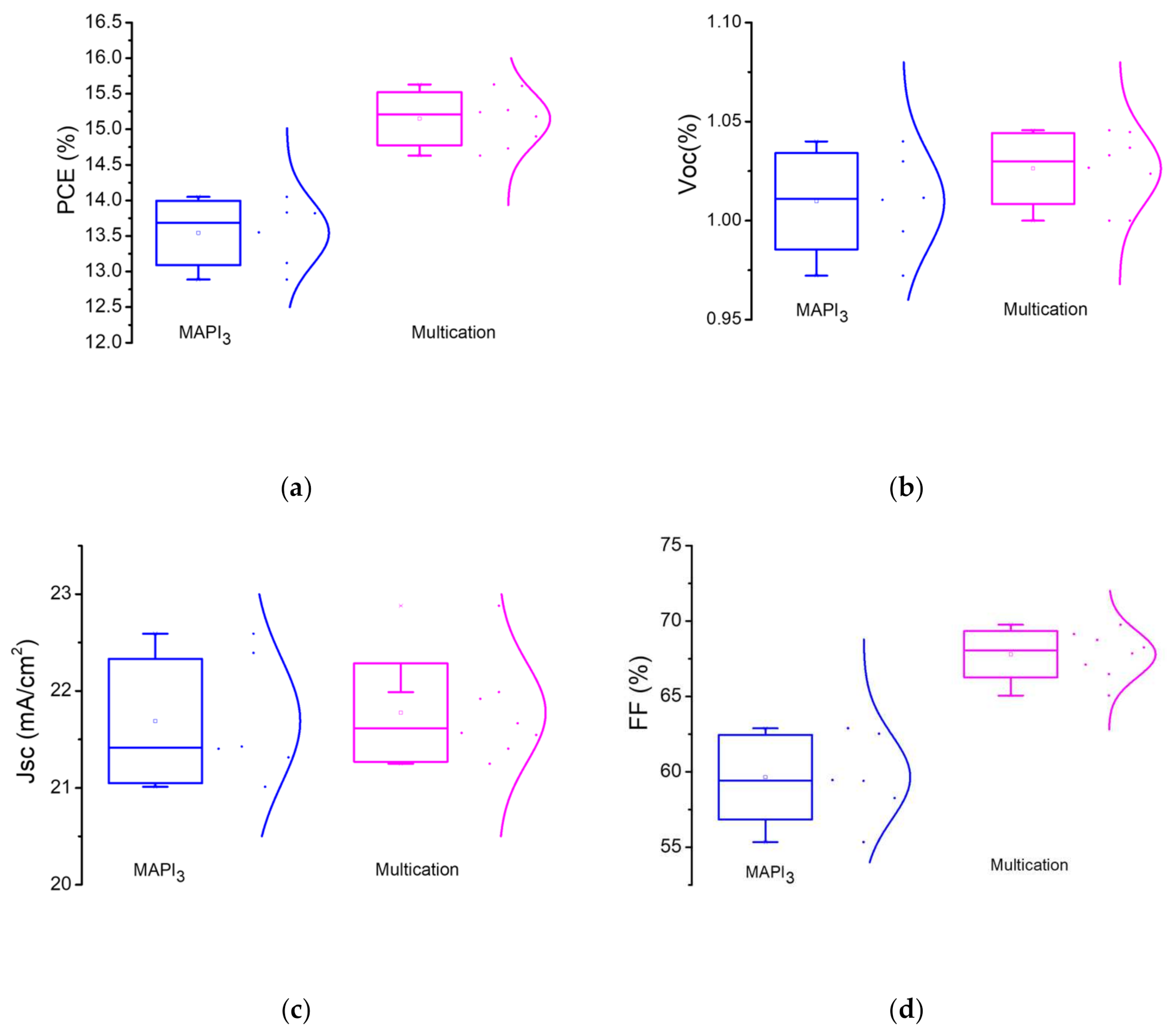
Statistic PV parameters of the multication and MAPbI3 PSCs are also presented in Figure 6. The comparison shows higher PCE values for multication PSCs vs. MAPbI3 devices which mainly attributed to enhancement of FF. Such improvement of the FF would be attributed to better perovskite/NiOX interface. Under 1 Sun, the VOC observed ranges from 1 to 1.05 V for multication perovskite, whereas for MAPbI3 it is 0.97 to 1.04 V. Table 2 illustrates the statistics of the main output parameters of perovskite devices with inverted planar structure.
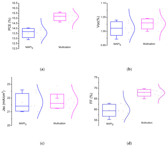
Figure 6.
Statistical photovoltaic parameters of the of MAPbI3 perovskite vs. multication perovskite: (a) PCE; (b) VOC; (c) JSC; (d) Fill Factor.
The inverted planar PSCs based on sequential deposition of multication perovskite absorber with 30 min dipping time exhibits a 15.6% PCE. This is currently a valuable PCE for two-step deposited p-i-n PSCs with NiOX hole selective layer, in which the absorber is made in ambient conditions (relative humidity—50–60%).
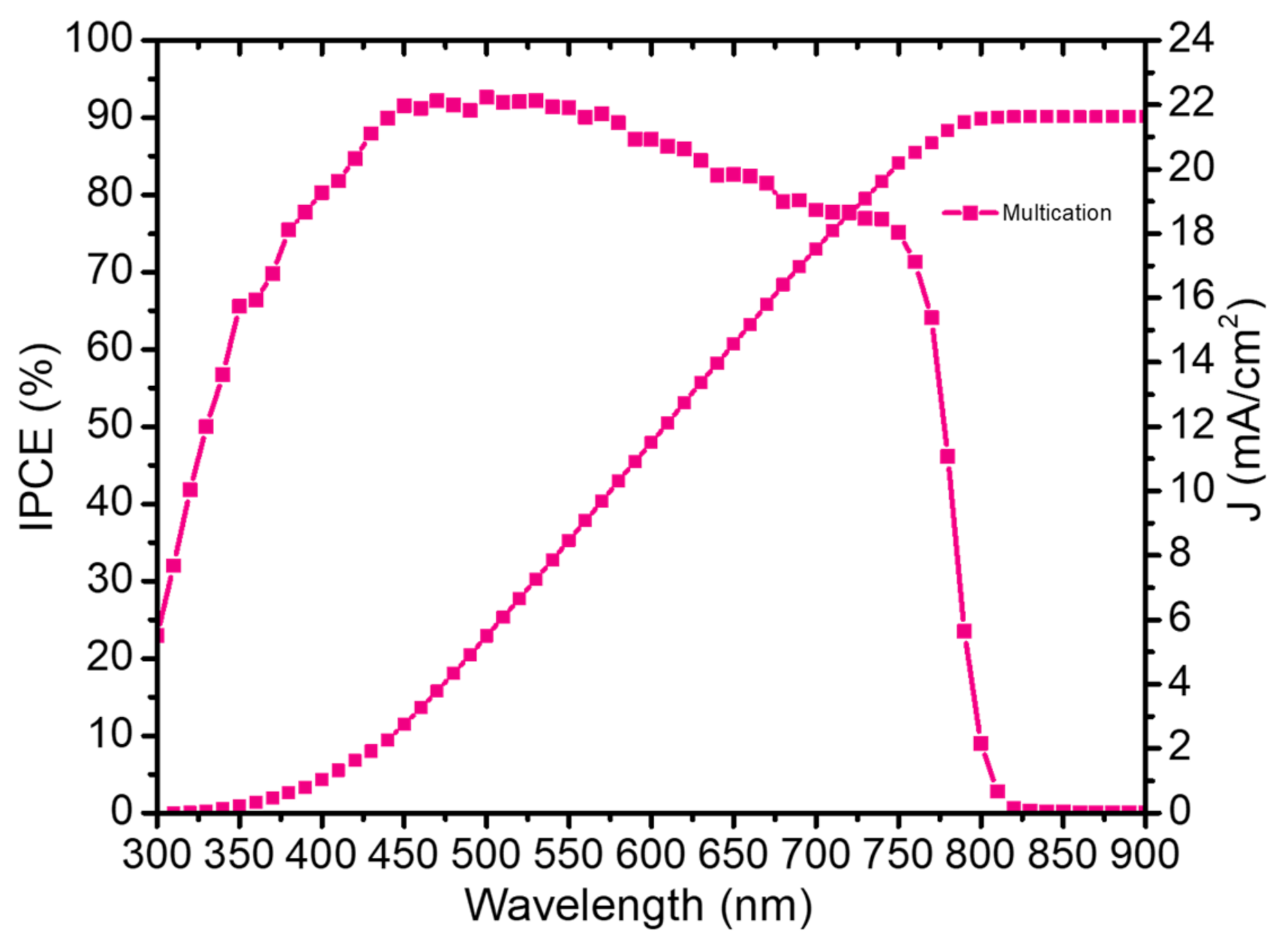
This max value of the JSC is also confirmed by the External quantum efficiency (EQE) spectrum of as presented in Figure 7. The integrated JSC of multication perovskite was calculated to be 21.628 mA/cm2, which is within a reasonable range from the J–V measurements at 1 Sun.
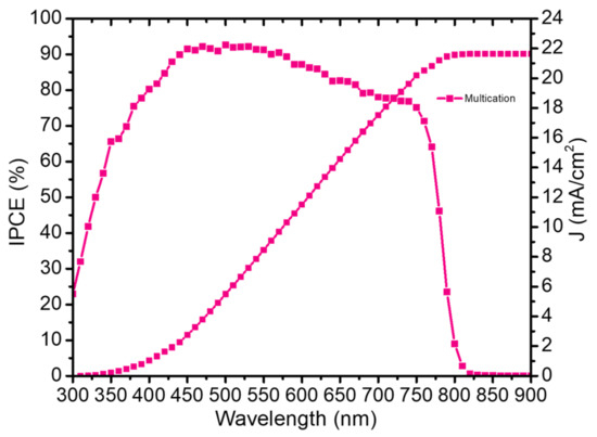
Figure 7.
EQE measurement of the best multication solar cells fabricated by two-step deposition.
3.4. Transient Photovoltage (TPV) and Transient Photocurrent (TPC)
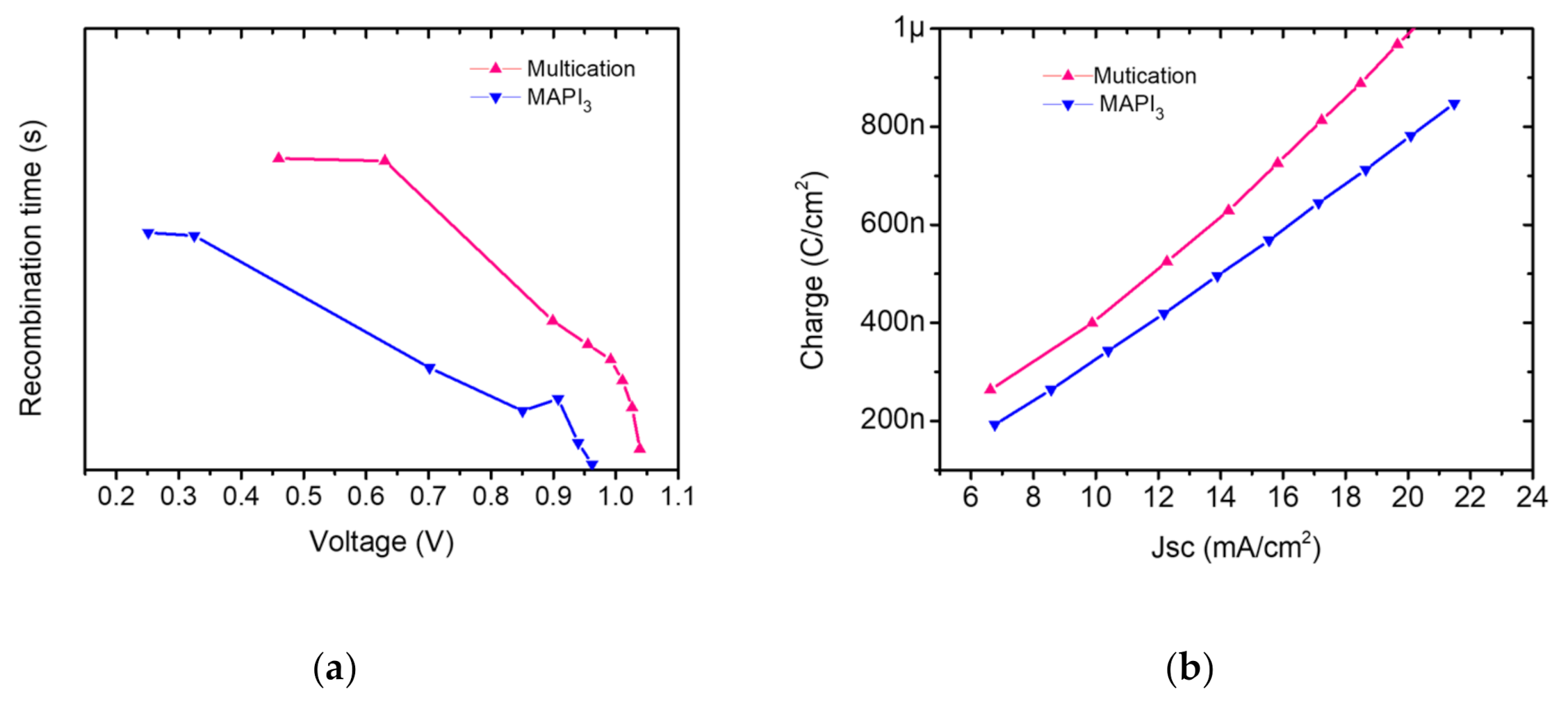
To study the charge extraction and recombination statistics, the methods of transient photovoltage (TPV) under open circuit (VOC) condition and charge carrier extraction (CE) were applied to our cells. The TPV is based on identifying the charge carrier lifetime upon monitoring the photovoltage decay. In Figure 8a multication PSC showed higher recombination time (longer lifetime) than MAPbI3 PSC justifying the J–V-measurements. This is explained by a better film quality in multication perovskites, which leads to reduced recombination within the films and longer diffusion lengths and recombination times. This is also evident because the VOC and FF of multication perovskite is higher than MAPbI3 [22,64]. Jia-Shang Zhao et al. explained that in mixed-cation, mixed-halide perovskite the carrier recombination process occurs with distinct processes (biphasic trap assisted carrier recombination mechanism) in the device: the two perovskite phases coexisting in the film dominate at different potentials, with the methylammonium lead iodide phase showing the fastest recombination dynamics [71].
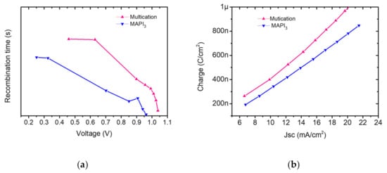
Figure 8.
(a) Recombination time versus voltage, evaluated from transient photovoltage decay analysis of the PSCs. (b) Charge extraction curves of the PSCs obtained from transient photocurrent fall/rise analysis.
Charge carrier kinetics in perovskite cells were identified by transient photocurrent (TPC) method under solar relevant conditions. The extracted charges from the photocurrent decay for each kind of perovskite are plotted in Figure 8b. It is evident that charge extraction is better in the optimized multication perovskite compared to MAPbI3, confirming the important role of charge extraction in the photovoltaic performances (Figure 6).
4. Conclusions
In conclusion, in this paper we showed for the first time a sequential deposition for multication perovskite out of glove-box on inverted structure p-i-n perovskite solar cells with nickel oxide hole transporting layer. We adapted the crystal engineering approach to fabricate inverted perovskite solar cells in ambient conditions in order to achieve high quality perovskite films with large grain size. We showed that the dipping time and annealing for the second step of the deposition process is a crucial element that helps getting large grains and therefore higher short-circuit current densities. The optimized procedure, consisting in a 30 min dipping time for multication perovskite, yields a champion device with power conversion efficiency of 15.6%. The sequential deposited MAPbI3 perovskite solar cells on planar NiOX (HTL) reached exceeding 14%. The comparison with the reference, methylammonium lead triiodide perovskite, shows that multication PSCs have improved performance, confirmed by charge extraction and carrier lifetime measurements. Multiple layer NiOx is crucial parameter to get better FF, Jsc, and efficiency. We have proved that for sequential deposition we need the thicker NiOx layer. However, the FF of the cells still need further improvement, which will be addressed in future developments. This work could pave the way for high efficiency large area out of the glove-box fully solution-processed, low cost fabrication perovskite solar devices.
Supplementary Materials
The following are available online at https://www.mdpi.com/1996-1073/14/6/1751/s1, Figure S1: Statistical photovoltaic parameters of the of MAPbI3 perovskite applying PCBM and BCP outside and inside glove-box: (a)—PCE, (b)—JSC (c)—Fill Factor, and (d)—VOC, Table S1: The best parameters and average values of MAPbI3 perovskite applying PCBM and BCP outside and inside glove-box: (a)—PCE, (b)—JSC (c)—Fill Factor, and (d)—VOC, Figure S2a—Absorbance of multication perovskite films (different dipping time), Figure S2b—PL of multication films on NiOX/FTO (different dipping time), Figure S3—(a) Multication perovskite: Jsc dependence on dipping time in multication solution; (b–e)—Electrical parameter statistics for the investigated multication perovskite-based device acquired at 1 Sun irradiation. The cell active area is 0.16 cm2. Figure S4—J–V-plots of two-step (a)—Multication and (b)—pure MAPbI3 perovskite solar cells, Figure S5—Pb and PbX2 layer, perovskite layers.
Author Contributions
I.E. wrote the original draft of the manuscript; I.E. and N.Y.N. performed the experiments and measurements; I.E. and N.Y.N. analyzed and extracted the data; I.E., N.Y.N., E.L. and A.D.C. wrote, reviewed, and edited the final draft; I.E. prepared samples for SEM measurement; E.D.B. and E.K. performed the SEM measurement; L.L. synthesized the NiOx; A.D.C. and N.Y.N. conceived the idea; N.Y.N. and A.D.C. supervised the work; A.D.C. project administration and funded acquisition. All authors have read and agreed to the published version of the manuscript.
Funding
“This research was funded by the Italian Ministry of Economic Development in the framework of the Operating Agreement with ENEA for Research on the Electric System” and by Ministry of Science and Higher Education of the Russian Federation in the framework of MegaGrant (no. 075-15-2019-872/074- 02-2018-327).
Institutional Review Board Statement
Not applicable.
Informed Consent Statement
Not applicable.
Data Availability Statement
The data presented in this study are available on request from the corresponding author.
Acknowledgments
I.E., L.L. and A.D.C. gratefully acknowledge the financial support from the Ministry of Science and Higher Education of the Russian Federation in the framework of MegaGrant (no. 075-15-2019-872/074- 02-2018-327). N.Y.N. acknowledge the Italian Ministry of Economic Development in the framework of the Operating Agreement with ENEA for Research on the Electric System.
Conflicts of Interest
The authors declare no conflict of interest.
References
- Di Carlo, A.; Lamanna, E.; Yaghoobi Nia, N. Photovoltaics. EPJ Web Conf. 2020, 246, 00005. [Google Scholar] [CrossRef]
- Zendehdel, M.; Yaghoobi Nia, N.; Yaghoubinia, M. Emerging Thin Film Solar Panels. In Reliability and Ecological Aspects of Photovoltaic Modules; IntechOpen: London, UK, 2020; pp. 163–228. ISBN 9780081027622. [Google Scholar]
- Yaghoobi Nia, N.; Saranin, D.; Palma, A.L.; Di Carlo, A. Perovskite solar cells. In Solar Cells and Light Management; Francesco Enrichi, G.C.R., Ed.; Elsevier: Amsterdam, The Netherlands, 2020; pp. 163–228. ISBN 9780081027622. [Google Scholar]
- Kojima, A.; Teshima, K.; Shirai, Y.; Miyasaka, T. Organometal halide perovskites as visible-light sensitizers for photovoltaic cells. J. Am. Chem. Soc. 2009, 131, 6050–6051. [Google Scholar] [CrossRef]
- NREL Best Research-Cell Efficiency Chart|Photovoltaic Research|NREL. Available online: https://www.nrel.gov/pv/cell-efficiency.html (accessed on 13 September 2019).
- Yaghoobi Nia, N.; Zendehdel, M.; Abdi-Jalebi, M.; Castriotta, L.A.; Kosasih, F.U.; Lamanna, E.; Abolhasani, M.M.; Zheng, Z.; Andaji-Garmaroudi, Z.; Asadi, K.; et al. Beyond 17% stable perovskite solar module via polaron arrangement of tuned polymeric hole transport layer. Nano Energy 2021, 82, 105685. [Google Scholar] [CrossRef]
- Li, J.; Wang, H.; Chin, X.Y.; Dewi, H.A.; Vergeer, K.; Goh, T.W.; Lim, J.W.M.; Lew, J.H.; Loh, K.P.; Soci, C.; et al. Highly Efficient Thermally Co-evaporated Perovskite Solar Cells and Mini-modules. Joule 2020, 4, 1035–1053. [Google Scholar] [CrossRef]
- Kulkarni, S.A.; Baikie, T.; Boix, P.P.; Yantara, N.; Mathews, N.; Mhaisalkar, S. Band-gap tuning of lead halide perovskites using a sequential deposition process. J. Mater. Chem. A 2014, 2, 9221–9225. [Google Scholar] [CrossRef]
- Yang, T.C.J.; Fiala, P.; Jeangros, Q.; Ballif, C. High-Bandgap Perovskite Materials for Multijunction Solar Cells. Joule 2018, 2, 1421–1436. [Google Scholar] [CrossRef]
- De Wolf, S.; Holovsky, J.; Moon, S.J.; Löper, P.; Niesen, B.; Ledinsky, M.; Haug, F.J.; Yum, J.H.; Ballif, C. Organometallic halide perovskites: Sharp optical absorption edge and its relation to photovoltaic performance. J. Phys. Chem. Lett. 2014, 5, 1035–1039. [Google Scholar] [CrossRef]
- Li, Y.; Ji, L.; Liu, R.; Zhang, C.; Mak, C.H.; Zou, X.; Shen, H.H.; Leu, S.Y.; Hsu, H.Y. A review on morphology engineering for highly efficient and stable hybrid perovskite solar cells. J. Mater. Chem. A 2018, 6, 12842–12875. [Google Scholar] [CrossRef]
- Guo, Z.; Zhou, N.; Williams, O.F.; Hu, J.; You, W.; Moran, A.M. Imaging Carrier Diffusion in Perovskites with a Diffractive Optic-Based Transient Absorption Microscope. J. Phys. Chem. C 2018, 19, 10650–10656. [Google Scholar] [CrossRef]
- Wu, B.; Zhou, Y.; Xing, G.; Xu, Q.; Garces, H.F.; Solanki, A.; Goh, T.W.; Padture, N.P.; Sum, T.C. Long Minority-Carrier Diffusion Length and Low Surface-Recombination Velocity in Inorganic Lead-Free CsSnI3Perovskite Crystal for Solar Cells. Adv. Funct. Mater. 2017, 27, 1604818. [Google Scholar] [CrossRef]
- Sherkar, T.S.; Momblona, C.; Gil-Escrig, L.; Ávila, J.; Sessolo, M.; Bolink, H.J.; Koster, L.J.A. Recombination in Perovskite Solar Cells: Significance of Grain Boundaries, Interface Traps, and Defect Ions. ACS Energy Lett. 2017, 2, 1214–1222. [Google Scholar] [CrossRef] [PubMed]
- Chen, X.; Lu, H.; Yang, Y.; Beard, M.C. Excitonic Effects in Methylammonium Lead Halide Perovskites. J. Phys. Chem. Lett. 2018, 10, 2595–2603. [Google Scholar] [CrossRef]
- Dou, B.; Whitaker, J.B.; Bruening, K.; Moore, D.T.; Wheeler, L.M.; Ryter, J.; Breslin, N.J.; Berry, J.J.; Garner, S.M.; Barnes, F.S.; et al. Roll-to-Roll Printing of Perovskite Solar Cells. ACS Energy Lett. 2018, 10, 2558–2565. [Google Scholar] [CrossRef]
- Mathies, F.; Eggers, H.; Richards, B.S.; Hernandez-Sosa, G.; Lemmer, U.; Paetzold, U.W. Inkjet-Printed Triple Cation Perovskite Solar Cells. ACS Appl. Energy Mater. 2018, 1, 1834–1839. [Google Scholar] [CrossRef]
- Jiang, Y.; Wu, C.; Li, L.; Wang, K.; Tao, Z.; Gao, F.; Cheng, W.; Cheng, J.; Zhao, X.Y.; Priya, S.; et al. All electrospray printed perovskite solar cells. Nano Energy 2018, 53, 440–448. [Google Scholar] [CrossRef]
- Arain, Z.; Liu, C.; Yang, Y.; Mateen, M.; Ren, Y.; Ding, Y.; Liu, X.; Ali, Z.; Kumar, M.; Dai, S. Elucidating the dynamics of solvent engineering for perovskite solar cells. Sci. China Mater. 2018, 62, 161–172. [Google Scholar] [CrossRef]
- Jeon, N.J.; Noh, J.H.; Kim, Y.C.; Yang, W.S.; Ryu, S.; Seok, S. Il Solvent engineering for high-performance inorganic-organic hybrid perovskite solar cells. Nat. Mater. 2014, 13, 897–903. [Google Scholar] [CrossRef]
- Gedamu, D.; Asuo, I.M.; Benetti, D.; Basti, M.; Ka, I.; Cloutier, S.G.; Rosei, F.; Nechache, R. Solvent-Antisolvent Ambient Processed Large Grain Size Perovskite Thin Films for High-Performance Solar Cells. Sci. Rep. 2018, 8, 12885. [Google Scholar] [CrossRef]
- Yaghoobi Nia, N.; Giordano, F.; Zendehdel, M.; Cinà, L.; Palma, A.L.; Medaglia, P.G.; Zakeeruddin, S.M.; Grätzel, M.; Di Carlo, A. Solution-based heteroepitaxial growth of stable mixed cation/anion hybrid perovskite thin film under ambient condition via a scalable crystal engineering approach. Nano Energy 2020, 69, 104441. [Google Scholar] [CrossRef]
- Yaghoobi Nia, N.; Zendehdel, M.; Cinà, L.; Matteocci, F.; Di Carlo, A. A crystal engineering approach for scalable perovskite solar cells and module fabrication: A full out of glove box procedure. J. Mater. Chem. A 2018, 6, 659–671. [Google Scholar] [CrossRef]
- Navazani, S.; Yaghoobi Nia, N.; Zendehdel, M.; Shokuhfar, A.; Di Carlo, A. Fabrication of high efficiency, low-temperature planar perovskite solar cells via scalable double-step crystal engineering deposition method fully out of glove box. Sol. Energy 2020, 206, 181–187. [Google Scholar] [CrossRef]
- Zhang, L.; Yuan, F.; Dong, H.; Jiao, B.; Zhang, W.; Hou, X.; Wang, S.; Gong, Q.; Wu, Z. One-Step Co-Evaporation of All-Inorganic Perovskite Thin Films with Room-Temperature Ultralow Amplified Spontaneous Emission Threshold and Air Stability. ACS Appl. Mater. Interfaces 2018, 10, 40661–40671. [Google Scholar] [CrossRef]
- Djurišić, A.B.; Liu, F.Z.; Tam, H.W.; Wong, M.K.; Ng, A.; Surya, C.; Chen, W.; He, Z.B. Perovskite solar cells—An overview of critical issues. Prog. Quantum Electron. 2017, 53, 1–37. [Google Scholar] [CrossRef]
- Shi, Z.; Jayatissa, A.H. Perovskites-based solar cells: A review of recent progress, materials and processing methods. Materials 2018, 11, 729. [Google Scholar] [CrossRef]
- Zhou, H.; Chen, Q.; Yang, Y. Vapor-assisted solution process for perovskite materials and solar cells. MRS Bull. 2015, 40, 667–673. [Google Scholar] [CrossRef]
- Casaluci, S.; Cinà, L.; Pockett, A.; Kubiak, P.S.; Niemann, R.G.; Reale, A.; Di Carlo, A.; Cameron, P.J. A simple approach for the fabrication of perovskite solar cells in air. J. Power Sources 2015, 297, 504–510. [Google Scholar] [CrossRef]
- Fan, P.; Gu, D.; Liang, G.X.; Luo, J.T.; Chen, J.L.; Zheng, Z.H.; Zhang, D.P. High-performance perovskite CH3NH3PbI3thin films for solar cells prepared by single-source physical vapour deposition. Sci. Rep. 2016, 6, 29910. [Google Scholar] [CrossRef]
- Bonomi, S.; Marongiu, D.; Sestu, N.; Saba, M.; Patrini, M.; Bongiovanni, G.; Malavasi, L. Novel Physical Vapor Deposition Approach to Hybrid Perovskites: Growth of MAPbI3 Thin Films by RF-Magnetron Sputtering. Sci. Rep. 2018, 8, 15388. [Google Scholar] [CrossRef]
- Wang, M.; Li, B.; Siffalovic, P.; Chen, L.C.; Cao, G.; Tian, J. Monolayer-like hybrid halide perovskite films prepared by additive engineering without antisolvents for solar cells. J. Mater. Chem. A 2018, 6, 15386–15394. [Google Scholar] [CrossRef]
- Liang, K.; Mitzi, D.B.; Prikas, M.T. Synthesis and Characterization of Organic-Inorganic Perovskite Thin Films Prepared Using a Versatile Two-Step Dipping Technique. Chem. Mater. 1998, 10, 403–411. [Google Scholar] [CrossRef]
- Burschka, J.; Pellet, N.; Moon, S.J.; Humphry-Baker, R.; Gao, P.; Nazeeruddin, M.K.; Grätzel, M. Sequential deposition as a route to high-performance perovskite-sensitized solar cells. Nature 2013, 499, 316–319. [Google Scholar] [CrossRef] [PubMed]
- Razza, S.; Castro-Hermosa, S.; Di Carlo, A.; Brown, T.M. Research Update: Large-area deposition, coating, printing, and processing techniques for the upscaling of perovskite solar cell technology. APL Mater. 2016, 4, 091508. [Google Scholar] [CrossRef]
- Khazaee, M.; Sardashti, K.; Sun, J.; Zhou, H.; Clegg, C.; Hill, I.G.; Jones, J.L.; Lupascu, D.C.; Mitzi, D.B. A Versatile Thin-Film Deposition Method for Multidimensional Semiconducting Bismuth Halides. Chem. Mater. 2018, 30, 3538–3544. [Google Scholar] [CrossRef]
- Taheri, B.; Nia, N.Y.; Agresti, A.; Pescetelli, S.; Ciceroni, C.; Del Rio Castillo, A.E.; Cinà, L.; Bellani, S.; Bonaccorso, F.; Di Carlo, A. Graphene-engineered automated sprayed mesoscopic structure for perovskite device scaling-up. 2D Mater. 2018, 5, 045034. [Google Scholar] [CrossRef]
- Sardashti, M.K.; Zendehdel, M.; Nia, N.Y.; Karimian, D.; Sheikhi, M. High Efficiency MAPbI3 Perovskite Solar Cell Using a Pure Thin Film of Polyoxometalate as Scaffold Layer. ChemSusChem 2017, 10. [Google Scholar] [CrossRef]
- Levine, I.; Nayak, P.K.; Wang, J.T.-W.; Sakai, N.; Van Reenen, S.; Brenner, T.M.; Mukhopadhyay, S.; Snaith, H.J.; Hodes, G.; Cahen, D. Temperature-dependent Hysteresis in MAPbI3 Solar Cells. Adv. Energy Mater. 2016, 16399–16411. [Google Scholar] [CrossRef]
- Unger, E.L.; Hoke, E.T.; Bailie, C.D.; Nguyen, W.H.; Bowring, A.R.; Heumüller, T.; Christoforo, M.G.; McGehee, M.D. Hysteresis and transient behavior in current-voltage measurements of hybrid-perovskite absorber solar cells. Energy Environ. Sci. 2014, 7, 3690–3698. [Google Scholar] [CrossRef]
- Leijtens, T.; Eperon, G.E.; Pathak, S.; Abate, A.; Lee, M.M.; Snaith, H.J. Overcoming ultraviolet light instability of sensitized TiO2with meso-superstructured organometal tri-halide perovskite solar cells. Nat. Commun. 2013, 4, 2885. [Google Scholar] [CrossRef]
- Sohrabpoor, H.; Puccetti, G.; Gorji, N.E. UV Degradation and Recovery of Perovskite Solar Cells. RSC Adv. 2016, 6, 49328–49334. [Google Scholar] [CrossRef]
- Calabrò, E.; Matteocci, F.; Palma, A.L.; Vesce, L.; Taheri, B.; Carlini, L.; Pis, I.; Nappini, S.; Dagar, J.; Battocchio, C.; et al. Low temperature, solution-processed perovskite solar cells and modules with an aperture area efficiency of 11%. Sol. Energy Mater. Sol. Cells 2018, 185, 136–144. [Google Scholar] [CrossRef]
- Wang, D.; Wright, M.; Elumalai, N.K.; Uddin, A. Stability of perovskite solar cells. Sol. Energy Mater. Sol. Cells 2016, 147, 255–275. [Google Scholar] [CrossRef]
- Liu, T.; Chen, K.; Hu, Q.; Zhu, R.; Gong, Q. Inverted Perovskite Solar Cells: Progresses and Perspectives. Adv. Energy Mater. 2016, 6, 1600457. [Google Scholar] [CrossRef]
- Zhao, Q.; Wu, R.; Zhang, Z.; Xiong, J.; He, Z.; Fan, B.; Dai, Z.; Yang, B.; Xue, X.; Cai, P.; et al. Achieving efficient inverted planar perovskite solar cells with nondoped PTAA as a hole transport layer. Org. Electron. 2019, 71, 106–112. [Google Scholar] [CrossRef]
- Reza, K.M.; Mabrouk, S.; Qiao, Q. A Review on Tailoring PEDOT:PSS Layer for Improved Performance of Perovskite Solar Cells. Proc. Nat. Res. Soc. 2018, 2, 02004. [Google Scholar] [CrossRef]
- Saliba, M.; Correa-Baena, J.P.; Wolff, C.M.; Stolterfoht, M.; Phung, N.; Albrecht, S.; Neher, D.; Abate, A. How to Make over 20% Efficient Perovskite Solar Cells in Regular (n-i-p) and Inverted (p-i-n) Architectures. Chem. Mater. 2018, 30, 4193–4201. [Google Scholar] [CrossRef]
- Petrović, M.; Maksudov, T.; Panagiotopoulos, A.; Serpetzoglou, E.; Konidakis, I.; Stylianakis, M.M.; Stratakis, E.; Kymakis, E. Limitations of a polymer-based hole transporting layer for application in planar inverted perovskite solar cells. Nanoscale Adv. 2019, 1, 3107–3118. [Google Scholar] [CrossRef]
- Pitchaiya, S.; Natarajan, M.; Santhanam, A.; Asokan, V.; Yuvapragasam, A.; Madurai Ramakrishnan, V.; Palanisamy, S.E.; Sundaram, S.; Velauthapillai, D. A review on the classification of organic/inorganic/carbonaceous hole transporting materials for perovskite solar cell application. Arab. J. Chem. 2018, 13, 2526–2557. [Google Scholar] [CrossRef]
- Kwon, U.; Kim, B.G.; Nguyen, D.C.; Park, J.H.; Ha, N.Y.; Kim, S.J.; Ko, S.H.; Lee, S.; Lee, D.; Park, H.J. Solution-Processible Crystalline NiO Nanoparticles for High-Performance Planar Perovskite Photovoltaic Cells. Sci. Rep. 2016, 6, 30759. [Google Scholar] [CrossRef]
- Guo, X.; Luo, G.; Liu, J.; Liao, C.; Wang, G.; Li, S. A 16.5% efficient perovskite solar cells with inorganic NiO film as hole transport material. IEEE J. Photovoltaics 2018, 8, 1039–1043. [Google Scholar] [CrossRef]
- Saranin, D.S.; Mazov, V.N.; Luchnikov, L.O.; Lypenko, D.A.; Gostishev, P.A.; Muratov, D.S.; Podgorny, D.A.; Migunov, D.M.; Didenko, S.I.; Orlova, M.N.; et al. Tris(ethylene diamine) nickel acetate as a promising precursor for hole transport layer in planar structured perovskite solar cells. J. Mater. Chem. C 2018, 6, 6179–6186. [Google Scholar] [CrossRef]
- Napari, M.; Huq, T.N.; Hoye, R.L.Z.; MacManus-Driscoll, J.L. Nickel oxide thin films grown by chemical deposition techniques: Potential and challenges in next-generation rigid and flexible device applications. InfoMat 2020, 1–41. [Google Scholar] [CrossRef]
- Xu, J.; Buin, A.; Ip, A.H.; Li, W.; Voznyy, O.; Comin, R.; Yuan, M.; Jeon, S.; Ning, Z.; McDowell, J.J.; et al. Perovskite-fullerene hybrid materials suppress hysteresis in planar diodes. Nat. Commun. 2015, 6, 7081. [Google Scholar] [CrossRef] [PubMed]
- Zhao, P.; Kim, B.J.; Jung, H.S. Passivation in perovskite solar cells: A review. Mater. Today Energy 2018, 7, 267–286. [Google Scholar] [CrossRef]
- Duan, J.; Liu, Z.; Zhang, Y.; Liu, K.; He, T.; Wang, F.; Dai, J.; Zhou, P. Planar perovskite FAxMA1-xPbI3 solar cell by two-step deposition method in air ambient. Opt. Mater. 2018, 85, 55–60. [Google Scholar] [CrossRef]
- Hu, L.; Peng, J.; Wang, W.; Xia, Z.; Yuan, J.; Lu, J.; Huang, X.; Ma, W.; Song, H.; Chen, W.; et al. Sequential Deposition of CH3NH3PbI3on Planar NiO Film for Efficient Planar Perovskite Solar Cells. ACS Photonics 2014, 7, 547–553. [Google Scholar] [CrossRef]
- Nawaz, A.; Erdinc, A.K.; Gultekin, B.; Tayyib, M.; Zafer, C.; Wang, K.; Akram, M.N. Morphology Study of Inverted Planar Heterojunction Perovskite Solar Cells in Sequential Deposition. Int. J. Energy Power Eng. 2016, 10, 922–926. [Google Scholar]
- Ashurov, N.; Oksengendler, B.L.; Maksimov, S.; Rashiodva, S.; Ishteev, A.R.; Saranin, D.S.; Burmistrov, I.N.; Kuznetsov, D.V.; Zakhisov, A.A. Current state and perspectives for organo-halide perovskite solar cells. Part 1. Crystal structures and thin film formation, morphology, processing, degradation, stability improvement by carbon nanotubes. A review. Mod. Electron. Mater. 2017, 3, 1–25. [Google Scholar] [CrossRef]
- Yaghoobi Nia, N.; Lamanna, E.; Zendehdel, M.; Palma, A.L.; Zurlo, F.; Castriotta, L.A.; Di Carlo, A. Doping Strategy for Efficient and Stable Triple Cation Hybrid Perovskite Solar Cells and Module Based on Poly(3-hexylthiophene) Hole Transport Layer. Small 2019, 15, 1904399. [Google Scholar] [CrossRef]
- Ünlü, F.; Jung, E.; Haddad, J.; Kulkarni, A.; Öz, S.; Choi, H.; Fischer, T.; Chakraborty, S.; Kirchartz, T.; Mathur, S. Understanding the interplay of stability and efficiency in A-site engineered lead halide perovskites. APL Mater. 2020, 8, 070901. [Google Scholar] [CrossRef]
- Holzhey, P.; Yadav, P.; Turren-Cruz, S.H.; Ummadisingu, A.; Grätzel, M.; Hagfeldt, A.; Saliba, M. A chain is as strong as its weakest link–Stability study of MAPbI3 under light and temperature. Mater. Today 2019, 29, 10–19. [Google Scholar] [CrossRef]
- Saliba, M.; Matsui, T.; Seo, J.-Y.; Domanski, K.; Correa-Baena, J.-P.; Nazeeruddin, M.K.; Zakeeruddin, S.M.; Tress, W.; Abate, A.; Hagfeldt, A.; et al. Cesium-containing triple cation perovskite solar cells: Improved stability, reproducibility and high efficiency. Energy Environ. Sci. 2016, 9, 1989–1997. [Google Scholar] [CrossRef]
- Chen, Q.; De Marco, N.; Yang, Y.; Song, T.B.; Chen, C.C.; Zhao, H.; Hong, Z.; Zhou, H.; Yang, Y. Under the spotlight: The organic-inorganic hybrid halide perovskite for optoelectronic applications. Nano Today 2015, 10, 355–396. [Google Scholar] [CrossRef]
- Guo, Y.; Yin, X.; Liu, J.; Chen, W.; Wen, S.; Que, M.; Tian, Y.; Yang, Y.; Que, W. Effect of the post-annealing temperature on the thermal-decomposed NiOx hole contact layer for perovskite solar cells. J. Adv. Dielectr. 2018, 8, 1–6. [Google Scholar] [CrossRef]
- Wang, M.H.; Jiang, X.Q.; Bian, J.M.; Feng, Y.L.; Wang, C.; Huang, Y.; Zhang, Y.D.; Shi, Y.T. High-Performance and Stable Mesoporous Perovskite Solar Cells via Well-Crystallized FA(0.85)MA(0.15)Pb(I0.8Br0.2)(3). ACS Appl. Mater. Interfaces 2019, 3, 2989–2996. [Google Scholar] [CrossRef]
- Nazem, H.; Dizaj, H.P.; Gorji, N.E. Modeling of Jsc and Voc versus the grain size in thin film and perovskite solar cells. Superlattices Microstruct. 2019, 128, 421–427. [Google Scholar] [CrossRef]
- Nie, W.; Tsai, H.; Asadpour, R.; Blancon, J.C.; Neukirch, A.J.; Gupta, G.; Crochet, J.J.; Chhowalla, M.; Tretiak, S.; Alam, M.A.; et al. High-efficiency solution-processed perovskite solar cells with millimeter-scale grains. Science 2015, 347, 522–525. [Google Scholar] [CrossRef]
- Abdi-Jalebi, M.; Dar, M.I.; Senanayak, S.P.; Sadhanala, A.; Andaji-Garmaroudi, Z.; Pazos-Outón, L.M.; Richter, J.M.; Pearson, A.J.; Sirringhaus, H.; Grätzel, M.; et al. Charge extraction via graded doping of hole transport layers gives highly luminescent and stable metal halide perovskite devices. Sci. Adv. 2019, 5, eaav2012. [Google Scholar] [CrossRef]
- Zhao, J.S.; Wang, H.Y.; Yu, M.; Hao, M.Y.; Yuan, S.; Qin, Y.; Fu, L.M.; Zhang, J.P.; Ai, X.C. Charge carrier recombination dynamics in a bi-cationic perovskite solar cell. Phys. Chem. Chem. Phys. 2019, 21, 5409–5415. [Google Scholar] [CrossRef]
Publisher’s Note: MDPI stays neutral with regard to jurisdictional claims in published maps and institutional affiliations. |
© 2021 by the authors. Licensee MDPI, Basel, Switzerland. This article is an open access article distributed under the terms and conditions of the Creative Commons Attribution (CC BY) license (http://creativecommons.org/licenses/by/4.0/).

