
Gate Drive Controller for Low Voltage DC Hybrid Circuit Breaker


School of EE & Control Engineering, Kongju National University, Budae-dong, Seobuk-gu, Cheonan-si 31080, Chungnam, Korea
Energies 2021, 14(6), 1753; https://doi.org/10.3390/en14061753
Submission received: 18 February 2021
/
Revised: 11 March 2021
/
Accepted: 18 March 2021
/
Published: 22 March 2021
(This article belongs to the Special Issue DC Circuit Breaker Technologies State of Art)
Abstract
:With the advent of direct current (DC) loads such as LED lighting, IT equipment, electric vehicles, and DC powers generated from renewable energy sources, low voltage DC (LVDC) distribution system is becoming a hot issue. One of the hurdles in the LVDC distribution system is arc flash at the contact points that occurs during the circuit is opening. Unlike alternating current, direct current has no zero points and sustains constantly. Therefore, there is a risk of electric fire due to continuous generating arcs when the load current is interrupted with an existing electrical contact type circuit breaker. Recently, the concept of a hybrid circuit breaker that takes advantage of traditional electrical contact type switch and the arcless semiconductor switch has been proposed, but how to cooperatively operate the two switches has become an issue. This paper analyzes the principle of a hybrid circuit breaker for blocking LVDC current and proposes a gate drive controller for it. Through 400V class LVDC cutoff test, the operation of the proposed hybrid circuit breaker is verified and the characteristics are analyzed.
1. Introduction
With the advent of electronic products in recent decades, the devices that we use have changed to work with direct current (DC) such as multimedia and mobile equipment, LED lighting, IT equipment, and electric vehicles. Moreover, in recent years, washing machines, refrigerators, fans, and heating/cooling systems adopt electric motors driven by DC power, improving speed control and energy efficiency. With the proliferation of renewable energy power systems using solar and wind energy, the form of power generation is also shifting to DC. With the latest improvements in battery technology, direct current has also become a widely recognized basic form of charge/discharge energy. Along with such outstanding technological advancement, the significant reduction in the cost of DC equipment has led to the expansion of the low voltage DC (LVDC) power distribution systems [1,2,3,4,5]. There are many benefits of DC compared with AC. For example, the peak voltage of DC is smaller than AC, so that the insulation is easy and larger power can be supplied with the same size of cable. There is no synchronization issue in DC, because DC has no frequency nor phase, so that management is easy. For DC loads, DC feed system is more efficient and low cost [6].
However, in order to widely spread the LVDC distribution systems, safety technologies for protecting human bodies and equipment from accidents are required. One of the distinctive features to ensure the safety of the DC system compared to the AC system is the arc phenomenon at the contact points that occurs when the mechanical switch is opened. Mechanical switches make or break electrical connection through two electrodes (fixed electrode and moving electrode). When the two electrodes are connected, switched-on contact resistance should be low enough to flow load current freely. When the two electrodes are disconnected, switched-off insulation resistance should be high enough to separate the load from electrical source. Thus, mechanical switches move around two extreme states during switching on and off, which cause severe electrical transient state.
As the electrodes are separated during the mechanical switch shutoff, the arc voltage, generated between the electrodes, causes a breakdown phenomenon in the air gap and induces a plasma arc current to cause the electrodes may be melted and stuck together [7,8]. If the mechanical switch is used in alternating current, the arc current itself becomes zero every half cycle. Therefore, if the gap between the two electrodes is sufficient, the isolation operation is easily performed by securing insulation. However, in the case of DC, there is no current zero point, so additional responsibility is required for the switch to reduce the load current to zero. To this end, an arc voltage higher than the power supply voltage must be formed across the electrodes of the DC switch. The high arc voltage formed on the electrodes increases the forces of the breaking arc and makes extinguishing the arc difficult. If the switch fails to extinguishing the arc current and fails to switching off, a high-temperature, high-pressure plasma arc current will cause a fire in the vicinity, and result in loss of life and property [9,10]. Therefore, there is a risk of electric fire due to continuous generating arcs when the load current is interrupted with an existing electrical contact type circuit breaker [11,12,13,14,15].
On the other hand, a switch using a semiconductor has the advantage of not accompanying an arc when the circuit is cut off, but there is a problem that the loss is large during conduction mode. Recently, the concept of a hybrid circuit breaker that takes advantages of the electrical contact type switch and the semiconductor switch has been proposed, but how to cooperatively operate the two switches has become an important issue [16].
This paper analyzes the principle of a hybrid circuit breaker for blocking LVDC circuits and proposes a gate drive controller for it. Through 400 V class LVDC cutoff test, the operation of the proposed hybrid circuit breaker is verified and characteristics are analyzed.
2. Principle and Power Circuit of Proposed Hybrid Circuit Breaker
Figure 1 shows the power circuit structure and breaking arc test waveform of a LVDC system with a pure contact type switch. The contact type switch has very low conduction loss and has been widely used as an AC switch. However, since there is no current zero point in DC, it is highly probable that an arc is generated for a very long time when breaking off as shown in Figure 1b, resulting in damage to personnel and equipment due to melting or strong heat of the contact point.
In Figure 1b, the rising waveform with time is the arc voltage that occurs between the contacts when breaking off, and the falling waveform is the arc current that penetrates the air between the contacts when breaking off. At the moment the contacts are opened, the load current tries to flow by forming an electric discharge path between the contacts. Electric discharge is classified into dark discharge, glow discharge, and arc discharge according to the magnitude level of the discharge current, and arc discharge occurs when the load current is 0.5 to ~1 A or more.
In order to generate an arc discharge, the arc initiating voltage of about 10 V is rapidly formed between the contacts, because a voltage to cause plasma generation by collision of electrons and air molecules is required [17]. On the contrary, the load current satisfies Kirchhoff’s voltage law as a current drop corresponding to the arc initiating voltage between the contacts at the moment when an arc initiates. Thus, when a power semiconductor switch with a turn-on-voltage drop of under the arc initiating voltage is connected in parallel to both ends of the electrical contact, the current flowing through the electrical contact is immediately bypassed to the semiconductor switch due to the arc initiating voltage (around 10 V) generated when the electrical contact is opened.
Figure 2 shows the concept of the proposed LVDC hybrid circuit breaker using this principle. Figure 2a shows the concept of the power circuit of the proposed LVDC hybrid circuit breaker. Here, VSW is the voltage across the mechanical switch, VCE is the voltage across the static switch, VG is the gate voltage of the static switch, VR is the voltage drop across the load resistor, and VL is the voltage drop across the load reactor. The bridge diode permits the load current flows to be bidirectional. Figure 2b shows the basic operation sequence of the proposed LVDC hybrid circuit breaker.
The operation sequence of the proposed LVDC hybrid circuit breaker is as follows;
Switch ON operation sequence:
- (1)
- Turn on the electrical contact type main switch (SWMain).
- (2)
- After a certain time delay, the semiconductor switch (IGBT) is turned on by giving an ON command to the gate of the semiconductor switch. At this time, when the electrical contact type main switch (SWMain) is turned on, the voltage (VCE) between the collector and emitter terminals of the semiconductor switch is almost zero. Thus, the semiconductor switch cannot be turned ON and the load current flows through the main switch. This means that the semiconductor switch is in a standby state.
Switch OFF operation sequence:
- (1)
- On the standby state where the ON command is given to the gate of the semiconductor switch, the electrical contact type main switch (SWMain) is turned off.
- (2)
- According to the arc generation principle, when the electrical contact type main switch is turned off, an arc voltage of about 10 V is about to be formed at both ends of the contact right before the arc occurs [12].
- (3)
- Since the voltage reaches enough to turn on the semiconductor switch (around 2 V) before the arc initiating voltage (around 10 V) is formed, the current flowing through the electrical contact type main switch is immediately commutated to the semiconductor switch that has already given the ON command to the gate.
- (4)
- When the electrical contact type main switch is sufficiently opened to secure the insulation distance, an OFF command is given to the gate of the semiconductor switch to turn it OFF without generating a breaking arc.
As described above, the proposed LVDC hybrid circuit breaker has high conduction efficiency because current flows through the lossless contact points during ON state, and does not generate arcs at both ends of the contact points because semiconductor switch commutates and breaks the load current during OFF operation.
3. Gate Drive Control for Hybrid Circuit Breaker
The concept of a gate drive control circuit for the LVDC hybrid circuit breaker proposed in Figure 3 is explained. The electrical contact type switch consists of two pairs of switches: the main switch (SWMain) and the auxiliary switch (SWAux). A time delay circuit in the auxiliary switch branch operating in parallel with the main switch delays the ON/OFF command applied to the gate of the semiconductor switch (IGBT). As for the time delay circuit, a timer relay can be used as shown in Figure 3a, or a time delay by RC circuit as shown in Figure 3b can be used.
Figure 4 shows the concept of ON and OFF characteristics of a voltage-driven semiconductor switch. In voltage-driven semiconductor switches such as IGBTs and power MOSFETs, the state of the switch is determined by the magnitude of the voltage applied to the gate. As shown in Figure 4, when the voltage applied to the gate is between zero and the threshold voltage value (VGS(TH)), it does not conduct. When the voltage applied to the gate exceeds the threshold value (VGS(TH)), it starts to ON, load current also starts to increase. When the gate voltage exceeds fully turn on value (VGS(ON)), it is completely ON and 100% of the load current flows. Therefore, as shown in Figure 4, if the voltage applied to the gate (VGS) is gradually increased or gradually decreased, a time delay occurs during ON or OFF.
On the other hand, the RC circuit charges and discharges as shown in Figure 5a,b as the output of the gate driver changes to a high state voltage (Vcc) and a low state voltage (0 V). During the charging process in Figure 5a, the time it takes for the voltage across the capacitor (VCT) to reach 64% of the final high state voltage (Vcc) is equal to the time constant (τ = RTCT) of the RC circuit. For example, if the threshold value (VGS(TH)) of the gate voltage for turning ON the voltage-driven semiconductor switch (IGBT) is at 50% of the high state voltage (Vcc), the switch ON time delay (TON_Delay) of this semiconductor switch will be a little smaller than the time constant (τ = RTCT) of the RC circuit.
Conversely, the time it takes for the voltage across the capacitor (VCT) to reach 36% of the high state voltage (Vcc) during the discharging process in Figure 5b is equal to the time constant (τ = RTCT) of the RC circuit. For example, if the threshold value (VGS(TH)) of the gate voltage for turning OFF the voltage-driven semiconductor switch is at 50% of the high state voltage (Vcc), the switch OFF time delay (TOFF_Delay) of this semiconductor switch will be a little smaller than the time constant (τ = RTCT) of the RC circuit. Anyway, if the threshold value (VGS(TH)) of the gate voltage for turning on the voltage-driven semiconductor switch is set to be between 36% and 64% of the high state voltage (Vcc), the switching time delay of the semiconductor switch (IGBT) can be created in the vicinity of τ = RTCT. The time constant of the RC circuit is effective in making a short time delay of several ms in the semiconductor switch.
Figure 6 shows the mechanical components of the interlock switch that can be used as another method of implementing the operation of the proposed LVDC hybrid circuit breaker as a mechanical interlock switch. The proposed mechanical interlock implements a mechanical interlock of the main switch and the auxiliary switch by using one slider and two toggle switches. The main switch and the auxiliary switch are fixed to the frame, and the slider moves up and down linearly by external manipulation. The slider has two channels for turning each toggle switch ON/OFF, and each channel has two thresholds for turning each toggle switch ON or OFF. As shown in Figure 6, the lengths of the channel of the main switch and that of the auxiliary switch are different, so when turning on/off each toggle switch by moving the slider up and down, there is a difference in operating time of each switch. In other words, there is a delay in the ON/OFF operation of the two switches as much as the backlash depth shown in Figure 6. For example, when the backlash distance is 10 mm and the manipulation speed of the slider is 1 m/s, there is 10 ms of time delay between the main switch and the auxiliary switch.
In the case of the switch ON sequence, both the main switch and the auxiliary switch are in the OFF state in the initial condition (SWMain = OFF/SWAux = OFF). When the slider moves down and comes to state 1, as in Figure 6b, the main switch is first turned ON, but the auxiliary switch is still in the OFF state (SWMain = ON/SWAux = OFF). When the slider moves further down and comes to state 2, as in Figure 6c, both the main and auxiliary switches are turned on (SWMain = ON/SWAux = ON). Through this operation, a time delay is implemented by mechanical interlocking of the main switch and the auxiliary switch. This method of time delay by mechanical interlock may be applied to a simple structure wall mounted switch.
4. Feasibility Study
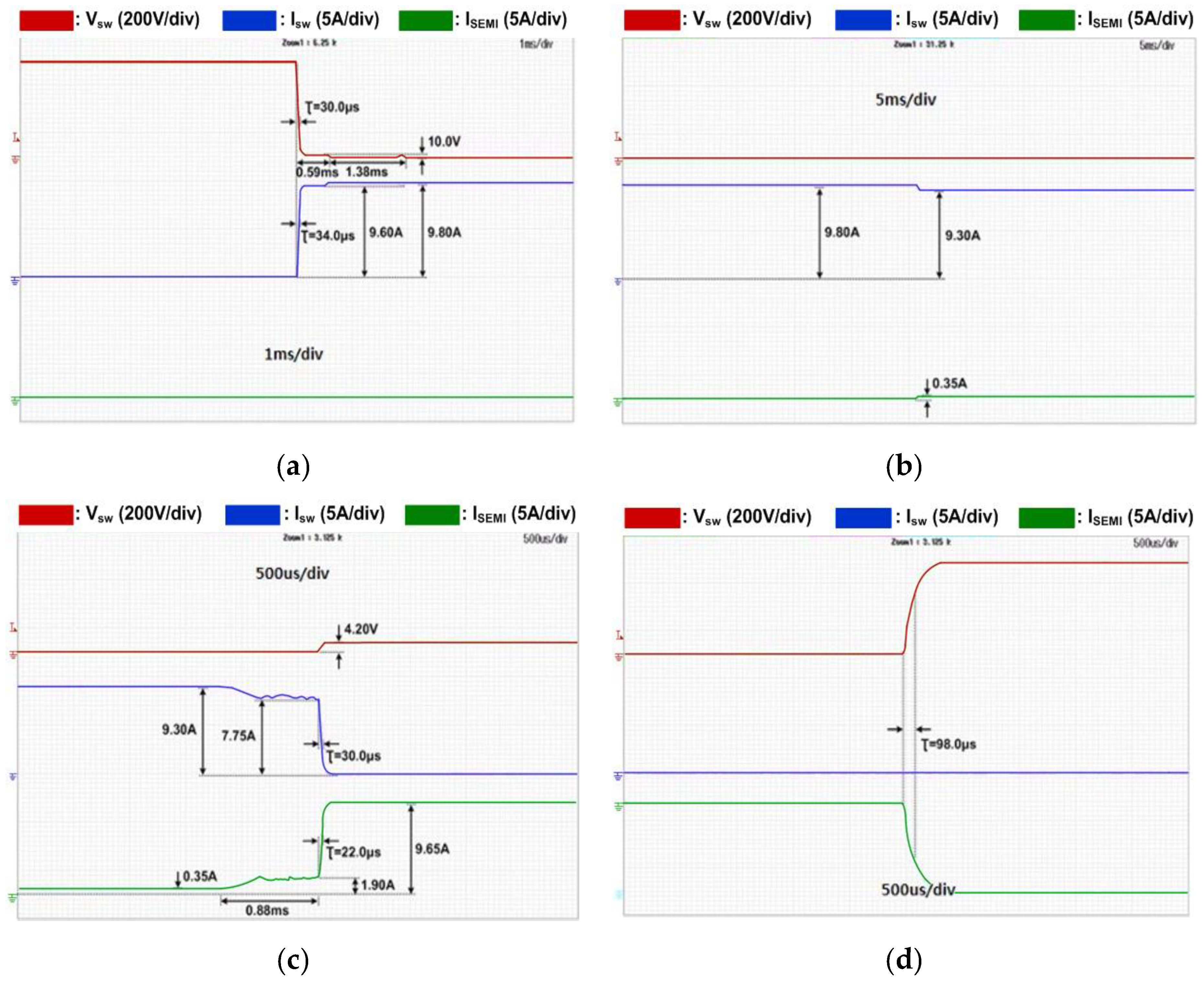
An experiment was performed to verify the gate drive control characteristics of the proposed LVDC hybrid circuit breaker. The power supply voltage used in the experiment was 400 Vdc and the load current was 10 A. Figure 7 shows the experimental waveform of the proposed LVDC hybrid circuit breaker. In the experiment, the time delay of the gate drive control circuit used a timer relay shown in Figure 3a. Due to the limitations of the space and time, this paper tested only a time delay gate driving circuit using a timer relay to see the validity of the proposed method. The study on the time delay by RC delay circuit and mechanical interlock, and the implementation and optimization of the driving circuit will be the subject of the next study.
Figure 7a shows the case of turning ON the main switch of the proposed LVDC hybrid circuit breaker to make the circuit. The voltage at both ends of the main switch, which was blocking the power supply voltage, has a time constant of about 30 us and falls sharply to zero. On the contrary, the load current rises and becomes conductive.
Figure 7b shows the situation in which the semiconductor switch is turned on while the main switch of the proposed LVDC hybrid circuit breaker is turned on and the load current flows. At this time, the voltage across the switch is almost unchanged and is in almost zero state. It can be seen that only a small amount (about 0.35 A) of the current flowing through the main switch flows to the semiconductor switch to which the gate signal is applied by the timer relay.
Figure 7c is the experimental waveform at the time when only the main switch is cut off in a situation where the load current was flowing through the proposed LVDC hybrid circuit breaker. When the main switch is opened, the voltage is about to rise to around 10 V in order to form an arc at both ends of the switch contact, but when the voltage reaches about 4.2 V in the middle, the semiconductor switch turns on and keeps the voltage of the switch contact at the turn-on-voltage drop of the the semiconductor switch, so an arc cannot be formed and the load current is immediately commutated to the semiconductor switch. In about 0.9 ms, the load current flowing through the main switch is completely commutated to the semiconductor switch to which the gate signal has already been applied.
Figure 7d shows that the gate signal applied to the semiconductor switch is turned off when the main switch of the proposed hybrid circuit breaker is completely open, and the load current flowing through the semiconductor switch falls to zero without an arc. Hence, the load current becomes completely blocked.
In this experiment, the time taken when the load current in the main switch is commutated to the semiconductor switch is about 0.9 ms. After then, for the semiconductor switching OFF time is about 0.01 ms, showing that the total cut-off time can be less than 1 ms. In addition, the breaking arc energy generated at the contact point of the main switch at the cutoff periode is less than 3.9 μWh, which is considered to have little effect on the burnout of the main switch contact. If the RC time delay circuit is used, it is expected that a minimum cut-off time can be implemented through an optimizing time delay.
5. Conclusions
This paper analyzed the principle of a hybrid circuit breaker in an LVDC system that lowers the loss during conduction and does not generate an arc when break off, and proposes a gate drive sequence controller. Through the 400 V/10 A class LVDC cutoff experiment, the operation of the proposed hybrid circuit breaker was verified and the characteristics were analyzed. As a result of the experiment, it was shown that the total breaking time can be less than 1 ms when the 400 V/10 A load is cut off. In addition, the break arc energy generated at the main switch contact at cut-off period is around 14 mW-s, which is significantly smaller than the break power of 4 kW, so it is judged that it hardly affects the damage of the main switch contacts. It is expected that the proposed LVDC hybrid circuit breaker can be used for normal arcless switches, arcless socket-out/plug, and wall mounted switches for residential houses. The proposed technology can be applied to LVDC voltage levels under 1500 V. The study on the time delay by RC delay circuit and mechanical interlock, and the implementation and optimization of the driving circuit will be the subject of the next study.
Funding
This work was supported in part by Basic Science Research Program through the National Research Foundation of Korea (NRF) funded by the Ministry of Education (Grants No. 2016R1D1A3B01008279).
Institutional Review Board Statement
Not applicable.
Data Availability Statement
Not applicable.
Conflicts of Interest
The author declares no conflict of interest.
References
- Pratt:, A.; Kumar, P.; Aldridge, T.V. Evaluation of 400V DC distribution in telco and data centers to improve energy efficiency. In Proceedings of the 29th International Telecommunications Energy Conference INTELEC 2007, Rome, Italy, 30 September–4 October 2007; pp. 32–39. [Google Scholar]
- Babasaki, T. Developing of Higher Voltage Direct-Current Power-feeding Prototype System. In Proceedings of the INTELEC 2009—31st International Telecommunications Energy Conference, Incheon, Korea, 18–22 October 2009; pp. 1–5. [Google Scholar]
- Rodriguez-Diaz, E.; Vasquez, J.C.; Guerrero, J.M. Intelligent DC homes in future sustainable energy systems: When efficiency and intelligence work together. IEEE Consum. Electron. Mag. 2016, 5, 74–80. [Google Scholar] [CrossRef] [Green Version]
- Dragicevic, T.; Vasquez, J.C.; Guerrero, J.M.; Skrlec, D. Advanced LVDC electrical power architectures and microgrids: A step toward a new generation of power distribution networks. IEEE Electrif. Mag. 2014, 2, 54–65. [Google Scholar] [CrossRef] [Green Version]
- Ghaffarpour Jahromi, M.; Mirzaeva, G.; Mitchell, S.D.; Gay, D. Powering mobile mining machines: DC versus AC power. IEEE Ind. Appl. Mag. 2016, 22, 63–72. [Google Scholar] [CrossRef] [Green Version]
- Whaite, S.; Grainger, B.; Kwasinski, A. Power Quality in DC Power Distribution Systems and Microgrids. Energies 2015, 8, 4378–4399. [Google Scholar] [CrossRef] [Green Version]
- Tsuruta, K.; Yanagi, K.; Shibata, S.; Yanagidaira, T.; Ikehata, T. Effect of axially symmetric magnetic fields for dynamics of low-current DC vacuum arc plasma. IEEE Trans. Plasma Sci. 2007, 35, 959–965. [Google Scholar] [CrossRef]
- Zhu, L.; Ji, S.; Liu, Y. Generation and developing process of low voltage series dc arc. IEEE Trans. Plasma Sci. 2014, 42, 2718–2719. [Google Scholar] [CrossRef]
- Lee, S.; Kim, D. A study on Low-Voltage DC circuit breakers. In Proceedings of the IEEE International Symposium on Industrial Electronics (ISIE), Taipei, Taiwan, 28–31 May 2013. [Google Scholar]
- Jadidian, J. A compact design for high voltage direct current circuit breaker. IEEE Trans. Plasma Sci. 2009, 37, 1084–1091. [Google Scholar] [CrossRef]
- Kim, H. DC distribution systems and circuit breaking technology. J. Korean Inst. Power Electron. 2010, 15, 40–46. [Google Scholar]
- Beak, S.; Yuba, T.; Kiryu, K.; Nakamura, A.; Miyazawa, H.; Noritake, M.; Hirose, K. Development of plug and socket-outlet for 400 volts direct current distribution system. In Proceedings of the 8th International Conference on Power Electronics—ECCE Asia, Jeju, Korea, 30 May–3 June 2011; pp. 218–222. [Google Scholar]
- Lee, S.; Kim, H. Development of DC Circuit Breaker using Magnet Arc Extinguisher. Trans. Korean Inst. Power Electron. 2012, 17, 21–26. [Google Scholar] [CrossRef] [Green Version]
- ABB Circuit-Breakers for Direct Current Applications. 2007. Available online: https://library.e.abb.com/public/de4ebee4798b6724852576be007b74d4/1SXU210206G0201.pdf (accessed on 20 January 2021).
- Strobl, C.; Kopf, H.; Mehl, R.; Ott, L.; Kaiser, J.; Gosses, K.; Schafer, M.; Rabenstein, R. Safety Concepts and Circuit Protection for LVDC Grids in Datacenters and in Telecommunications. In Proceedings of the 2018 IEEE International Telecommunications Energy Conference (INTELEC), Torino, Italy, 7–11 October 2018. [Google Scholar]
- Shukla, Z.A.; Demetriades, G.D. A survey on hybrid circuit-breaker topologies. IEEE Trans. Power Del. 2014, 30, 627–641. [Google Scholar] [CrossRef]
- Kim, W.H.; Kim, Y.J.; Kim, H.S. Arc Voltage and Current Characteristics in Low-Voltage Direct Current. Energies 2018, 11, 2511. [Google Scholar] [CrossRef] [Green Version]
Short Biography of Authors
 | Hyosung Kim received B.S. and M.S. degrees in the Dept. of Elec. Eng. from Seoul National University in Korea on 1981 and 1983, respectively. He received Ph.D. degree in the Dept. of Elec. Eng. from Chungbuk National University in Korea on 1995. From 1982 to 1986, he was employed at Tong-Yang Cement Mfg. Co., Korea, where he participated in factory automation and energy saving project. From 1996 to 1997, he was a visiting scholar in the Dept. of Elec. Eng. at Okayama University, Japan. From 2000 to 2001, he was an associate research professor in the Institute of Energy Technology at Aalborg University, Denmark. From 1997 to present, he is a tenured professor in the school of EE and Control Eng. at Kongju National University, Korea. He is interested in Power Quality, Static Compensators, Renewable energy, and DC Distribution Systems. |
Figure 1.
Power circuit and breaking arc of contact type switch; (a) Power circuit concept of contact type switch, (b) Breaking arc voltage/current waveform with resistive load.
Figure 1.
Power circuit and breaking arc of contact type switch; (a) Power circuit concept of contact type switch, (b) Breaking arc voltage/current waveform with resistive load.

Figure 2.
Concept of the proposed LVDC hybrid circuit breaker; (a) power circuit concept, (b) sequence of operations.
Figure 2.
Concept of the proposed LVDC hybrid circuit breaker; (a) power circuit concept, (b) sequence of operations.

Figure 3.
Concept of the proposed hybrid circuit breaker gate driving circuit; (a) Using timer relay, (b) Using R–C delay circuit.
Figure 3.
Concept of the proposed hybrid circuit breaker gate driving circuit; (a) Using timer relay, (b) Using R–C delay circuit.

Figure 4.
Concept of ON and OFF chacteristics of semiconductor switch (IGBT).
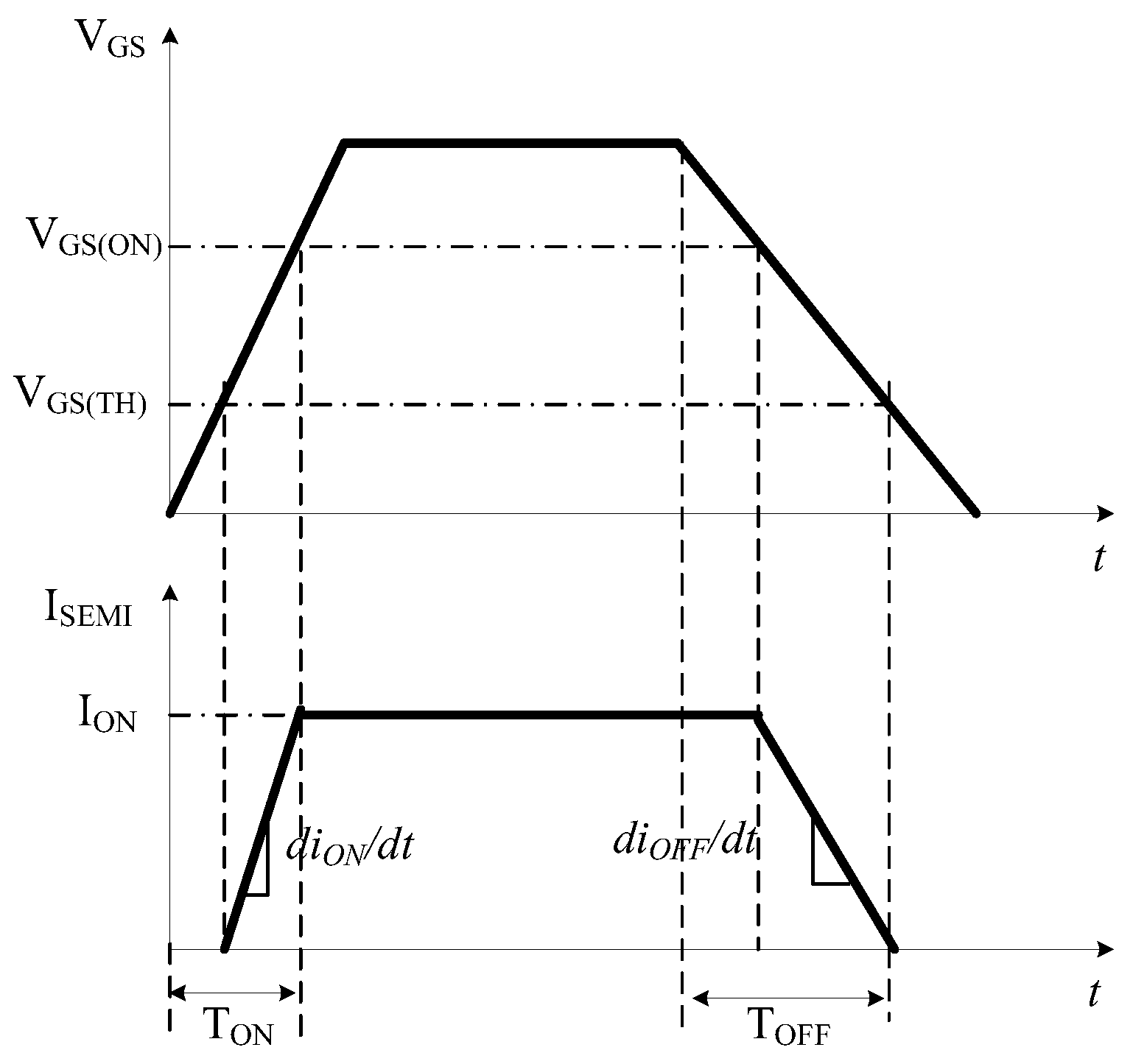
Figure 5.
RC charge/discharge and semiconductor switch (IGBT) ON and OFF time delay concept; (a) ON time delay of the semiconductor switch (IGBT) during charging (TON_Delay); (b) The OFF time delay of the semiconductor switch (IGBT) during the discharge process (TON_Delay).
Figure 5.
RC charge/discharge and semiconductor switch (IGBT) ON and OFF time delay concept; (a) ON time delay of the semiconductor switch (IGBT) during charging (TON_Delay); (b) The OFF time delay of the semiconductor switch (IGBT) during the discharge process (TON_Delay).
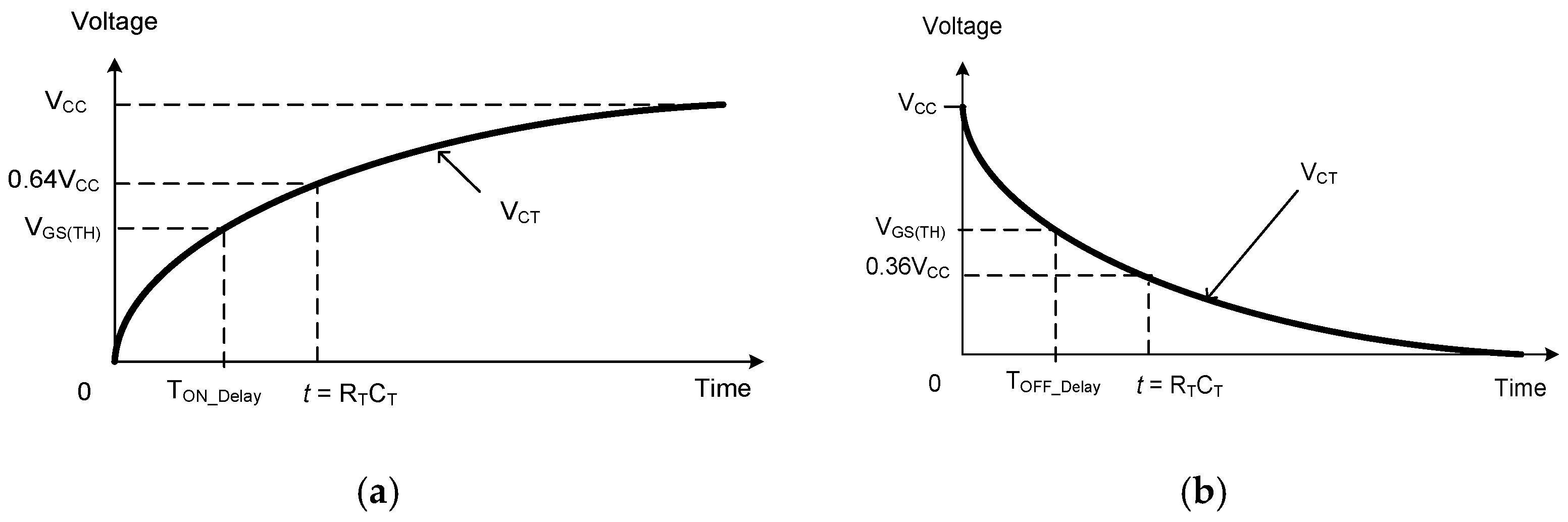
Figure 6.
Mechanical interlock concept between main switch (SWMain) and auxiliary switch (SWAux) using slider and toggle switch; (a) interlock structure; (b) State 1 (SWMain) = ON/(SWAux) = OFF; (c) State 2 (SWMain) = ON/(SWAux) = ON.
Figure 6.
Mechanical interlock concept between main switch (SWMain) and auxiliary switch (SWAux) using slider and toggle switch; (a) interlock structure; (b) State 1 (SWMain) = ON/(SWAux) = OFF; (c) State 2 (SWMain) = ON/(SWAux) = ON.

Figure 7.
Experimental waveform of the proposed hybrid circuit breaker; (a) main switch ON, (b) semiconductor switch ON, (c) main switch OFF, (d) semiconductor switch OFF.
Figure 7.
Experimental waveform of the proposed hybrid circuit breaker; (a) main switch ON, (b) semiconductor switch ON, (c) main switch OFF, (d) semiconductor switch OFF.
Publisher’s Note: MDPI stays neutral with regard to jurisdictional claims in published maps and institutional affiliations. |
© 2021 by the author. Licensee MDPI, Basel, Switzerland. This article is an open access article distributed under the terms and conditions of the Creative Commons Attribution (CC BY) license (http://creativecommons.org/licenses/by/4.0/).
Share and Cite
MDPI and ACS Style
Kim, H. Gate Drive Controller for Low Voltage DC Hybrid Circuit Breaker. Energies 2021, 14, 1753. https://doi.org/10.3390/en14061753
AMA Style
Kim H. Gate Drive Controller for Low Voltage DC Hybrid Circuit Breaker. Energies. 2021; 14(6):1753. https://doi.org/10.3390/en14061753
Chicago/Turabian StyleKim, Hyosung. 2021. "Gate Drive Controller for Low Voltage DC Hybrid Circuit Breaker" Energies 14, no. 6: 1753. https://doi.org/10.3390/en14061753
Note that from the first issue of 2016, this journal uses article numbers instead of page numbers. See further details here.