Abstract
This paper proposes a galvanically isolated dc-dc converter that can regulate the input voltage in a wide range. It is based on the series resonance dc-dc converter (SRC) topology and a novel boost rectifier. The proposed topology has a smaller number of semiconductors than its SRC-based existing topologies employing an ac-switch in the boost rectifier. The proposed dc-dc converter comprises only two diodes and one switch at the output side, while the existing solutions use two switches and two diodes to step up the voltage. The proposed converter boosts the input voltage within a single boosting interval in the positive half-cycle of the switching period. In addition, the resonant current in the negative half-cycle is sinusoidal, which could enhance the converter efficiency. The resonant capacitor voltage is clamped at the level of the output voltage. Therefore, the voltage stress of the capacitor could significantly reduce at various input voltage and power levels. This makes it perfect for distributed generation applications such as photovoltaics with wide variations of input voltage and power. The converter operates at the fixed switching frequency close to the resonance frequency to obtain the maximum efficiency at the nominal input voltage. The zero-voltage switching (ZVS) feature is achieved in the primary semiconductors, while the diodes in the output-side rectifier turn off at nearly zero current switching. The mathematical model and design guidelines of the proposed converter are discussed in the paper. The experimental results confirmed the theoretical analysis based on a 300 W prototype. The maximum efficiency of the converter was 96.8% at the nominal input voltage, and the converter has achieved a wider input voltage regulation range than that with the boosting cell comprising an ac-switch.
1. Introduction
With the rapid growth in the installation of photovoltaic (PV) modules in residential settings worldwide, the demand for new power converters with high efficiency and low cost is increasing [1]. This trend is expected to be complemented with the wider use of dc microgrids [2]. As a result, dc-dc converters are required to connect PV modules to a dc-bus of a dc-microgrid [3]. These converters have to maintain the following specifications: high power density, high efficiency, regulation of the wide range of variation in the input voltage, and compact size [3].
The converter with a wide input voltage regulation range could be capable of tracking the maximum available power of the PV module in various environmental and shading conditions. One of the promising candidates for this purpose is resonant converters like LLC [4,5,6] and the series resonant converter (SRC) [7,8,9], which are used in many industrial applications. However, LLC employs frequency modulation to regulate the voltage variation, and thus the design of the magnetic component becomes costly and complicated. The SRC has received more attention thanks to its simple design and control. Its implementation allows the resonant current to be discontinuous, i.e., the quality factor of the resonant tank is less than one. This implementation could perform the buck and boost functionality using different pulse width modulation (PWM) schemes with boost rectifier cells. The buck regulation requires the use of a special modulation at the input side, while the boost regulation requires a boosting rectifier cell, regulating the transformer leakage inductance current at the output side [10]. In addition, it can regulate the voltage while operating at a fixed switching frequency by adjusting the duty cycle of the semiconductors. Additionally, the voltage regulation range of the SRC depends on the switching cells utilized in the input and output sides [10,11,12]. This study is focused on the boost voltage regulation in the SRC using a boosting rectifier cell.
The boosting capabilities of the SRC can be upgraded by developing new boosting cells to be used at the output side. Since the resonant current on the high voltage side is relatively low, integrating the boosting cell on the secondary side of the isolation transformer minimizes losses. There are different investigated cells for the SRC aiming to improve the converter efficiency and the regulation range [13,14,15,16,17]. The bridgeless rectifier cell with two diodes and two metal oxide semiconductor field-effect transistors (MOSFETs) has been used widely in power factor correction applications. It has been used in [13], to step up the input voltage. Recently, it was demonstrated, in [11], that its regulation range is limited due to the possibility of reverse current flows in the same half-cycle due to the parasitic current path caused by the overlapped PWM scheme. The boosting cells in [14,15] have different PWM schemes, where the latter employed synchronous rectification to improve efficiency at the expense of cost and control complexity. In [16], the voltage boosting interval appears only at one half-cycle, and consequently, the resonance current has a sinusoidal waveform in the other half-cycle of the switching period, which avoids one hard turn-on of a transistor in the boosting cell. The configuration of the circuit in [17] employs two switches and two diodes. To implement the ac-switch, the two switches are connected as a back-to-back structure. In addition, two diodes and two capacitors are implemented with the voltage doubler rectifier. Contrary to the other boosting cells, the leakage inductance current rises linearly during the boosting interval like in the conventional boost converter. Although this boosting rectifier cell has a lower voltage stress on the MOSFETs and could reduce the switching losses, the voltage regulation range is substantially limited, especially at higher resonance inductance [12].
This paper modifies the boosting rectifier cells from [17], by removing one switch and rearranging the other switch and two diodes. Consequently, the proposed cell comprises only one MOSFET and two diodes in the configuration of the rectifier cell. The voltage stress on the resonance capacitor is clamped at the output voltage level, whatever the input voltage and power level. This resolves the main issue of the counterpart cells that could suffer from excessive stress on the resonant capacitor in case of overloads and regulation transients. In low-power conditions and lower dc voltage gains, the derived SRC employs only one diode, where the other diode is in the idle state. The modulation scheme applied to the proposed topology employs the forced half-resonance to enhance converter efficiency as the current has a half-wave sine waveform in one half-cycle of the switching period. The proposed circuit has various modes of operation that enable the converter to cope with the wide range of input voltages and power variations that are common for distributed generation applications. This paper will only handle regulating the low-input voltage, i.e., boosting condition.
The remaining content of the paper starts with Section 2 that comprehensively describes and analyzes the operation of the proposed topology in the boost mode, where the proposed boosting cell is used at the output side. Section 3 introduces the design guidelines and experimental results of the converter. Finally, Section 4 concludes the paper.
2. The Proposed Converter
2.1. Description of the Topology
The proposed topology is shown in Figure 1. The input capacitor, CIN, filters out the converter input current ripple and decouples the input voltage source, VIN. The front-end full-bridge comprises the semiconductors S1–S4 operating as a high-frequency inverter. The isolation transformer, TX, is employed to step up the input voltage by the factor of the turns ratio, n. It also provides galvanic isolation between the input and output sides to increase the safety level. The magnetizing current of the transformer, Im, which corresponds to the magnetizing inductance, Lm, helps achieve the soft-switching of the input-bridge semiconductors, as will be discussed later. The sum of the leakage inductance of the transformer, Llk, and the external resonant inductance, Lext, represents the resonance tank inductance, Lr = Llk + Lext. As a result of the magnetic integration of the isolation transformer and the resonant inductance, the size and cost of the converter will be decreased.

Figure 1.
Configuration of the proposed topology of series resonance dc-dc converter (SRC) with a single-switch boosting rectifier cell.
The resonance frequency of the converter, Fr, is defined in (1), where Cr refers to the resonant capacitance of the resonant tank. The boosting cell of the converter includes one MOSFET Q and two diodes (D1 and D2). The gating signal for Q must be adjusted regarding the biased state of the top diode D1. Next, the rectified voltage from the boosting cell is smoothed by the decoupling output capacitor, CO. The converter operates at a fixed switching frequency, FSW, which has to be selected at 5–10% lower than the resonance frequency to obtain the possible high conversion efficiency under the nominal input voltage [13].
The peak-to-peak voltage ripple value of the resonant capacitor, , can be defined as in (2). Although ∆VCr is mainly affected by the power level and input voltage of the converter, the maximum voltage across Cr does not exceed the value of the output voltage, VOUT, because the capacitor voltage will be clamped by the conducting bottom diode D2. In addition, the relation in (2) will not be valid in these conditions, and thus the maximum ripple this value cannot exceed ∆VCr(max) = 2nVIN. Therefore, the voltage stress of Cr is reduced at high power compared to the existing boosting rectifier cells. It is worth mentioning that D2 does not conduct as long as the capacitor voltage is less than the output voltage at any given time. The subsequent analysis of the proposed topology will be set according to these observations. The converter operation conditions depend on the operating point of the output power and the input voltage, as will be discussed later.
The following considerations are made to make the analysis simpler:
- Each primary side semiconductor has a parasitic output capacitance of Coss, while the other converter components are ideal;
- Negligible output voltage ripple;
- The output capacitance CO is much larger than Cr;
- The converter is lossless;
- The state variables of the converter are the resonance inductor current, iLr(t), and the resonance capacitor voltage, vCr(t).
2.2. Modes of Operation
The operation and design of the proposed converter are based on the discontinuous resonant current conditions in the case when the quality factor of the resonant tank is less than one under any load [10].
2.2.1. Operation at the Nominal Input Voltage (Pure-SRC)
As was mentioned in the Introduction, the SRC can operate both in the buck and boost modes. The operating point between them corresponds to the nominal input voltage when the given converter operates as a conventional non-controlled fixed-gain SRC with a purely sinusoidal current of the resonant tank. This is the normal state of the converter operation at which the output voltage is generated only by the boosting action from the isolation transformer. It will be referred to as pure-SRC in the remaining part of the paper. The equivalent circuit corresponds to a voltage doubler in the output-side cell with a single resonant capacitor.
The steady-state waveforms of the proposed converter are given in Figure 2. The diode D2 remains reverse biased during this condition where vCr(t) < VOUT at all the levels of the converter power. Thus, the current of the bottom diode equals zero, as shown in Figure 2. The switch Q duty cycle equals 0.5, excluding the short dead time. The value of ∆VCr can be accurately defined by Equation (2). The trajectory curve is close to a circular shape due to the sinusoidal contour of the resonance current and the capacitor voltage, as shown in Figure 3. The vertical axis corresponds to the resonant current multiplied by the characteristic impedance of the resonant tank, Zr. The resonant current reaches its maximum value when the resonant capacitor voltage equals zero and vice versa.

Figure 2.
Steady-state waveform of the proposed converter under the nominal input voltage (pure-SRC conditions).

Figure 3.
Trajectory curve of the converter state variables under the nominal input voltage (pure-SRC conditions).
The transistor Q gate signal follows that of the switches S2 and S3 to ensure that the top diode D1 is conducting during the positive half-cycle. When a positive voltage is applied to the transformer primary windings, the magnetizing current of the transformer, Im, has a positive slope and vice versa. The peak value of Im(max) depends on the input voltage and switching period as in (3). During the dead time between the switches in the same leg, the magnetizing inductance acts as a current source reflected onto the primary side to charge/discharge the parasitic output capacitance of the semiconductors, Coss. If the dead time is long enough, the primary switches are turned on at zero voltage switching in the next switching half-cycle. The diode D1 is turned off at nearly zero current switching at the end of the positive half-cycle as the resonance current drops down to zero and the converter enters the freewheeling state. The duration of the resonant current pulse feeding the load during the positive half-cycle depends on the operating power of the converter. At the same time, it occupies all the negative half-cycle due to the switch Q being turned on during this half-cycle.
2.2.2. Operation at the Input Voltages below the Nominal (Boost-SRC)
If the input source of the converter is a photovoltaic (PV) module, as an example, the terminal voltage is decreased under partial or opaque shading conditions. The reduced input voltage must be stepped up to the target dc-bus voltage by the converter. Therefore, the transistor Q is controlled with a duty cycle larger than 0.5 and uses the resonance inductor to boost the secondary winding voltage. During the conduction time part exceeding half of the switching period, the leakage inductance current is increasing, storing energy supplied from the input source. These operation conditions will be referred to as boost-SRC in the text below. There are three possible scenarios of the converter operation in the boost-SRC conditions: A, B, and C, depending on the critical time, tcri, at which the instantaneous value of the capacitor voltage reaches the output voltage starting from the beginning of the positive half-cycle. The steady-state waveforms and the trajectory curves of the state variables of the converter are given in Figure 4 and Figure 5, respectively, for three operation scenarios. During the boost-SRC condition, the converter will operate in the following modes:

Figure 4.
Steady-state waveforms of the proposed converter for three operation scenarios in the boost-SRC condition. (a) Scenario A: Forced half-resonance, (b) scenario B: Single-boosting mode, (c) scenario C: Double-boosting modes.
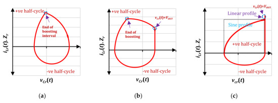
Figure 5.
Trajectory curves of the converter state variables for the three possible scenarios in the boost-SRC conditions. (a) Scenario A, (b) scenario B, (c) scenario C.
Mode I [< t ≤] (first part of the boosting interval): This represents the starting of the positive half-cycle as the transformer’s primary winding has a positive voltage by turning on the switches S1 and S4 at the instant t0 = 0. This instant will be used as a reference in all three operation scenarios for the boost-SRC conditions. The initial value of the resonance current is zero from the end of the previous half-cycle. Meanwhile, the capacitor voltage has an initial value of vCr(t0). The MOSFET Q continues conducting from the previous (negative) half-cycle. The top diode D1 is reverse biased when the switch Q is conducting, while the anode–cathode voltage across the bottom diode D2 is negative as vCr(t) is lower than VOUT. Therefore, D2 is reverse biased from the instant t0 as well. The equivalent circuit of the converter in this mode is depicted in Figure 6a for clarity. Lr and Cr are always resonating during this mode and start charging in a positive direction. The current charging profile of Lr follows the sinusoidal waveform. The time duration of this interval is equal to or less than the boosting time. This mode ends in either of two cases, whichever is sooner: the value of vCr(t) equals the output voltage, or the boosting interval ends. The equations of the state variables can be derived from the equivalent circuit as:
where is the characteristic impedance of the resonant tank, and is the resonant angular frequency.

Figure 6.
Equivalent circuits of the proposed converter in the boost-SRC conditions. (a) Mode I, (b) Mode II, (c) Mode III, (d) Mode IV, (e) Mode VI.
Mode II [< t ≤ t1] (remaining part of the boosting interval, if applicable): This mode has a probability of occurrence based on the operation scenario of the converter, as will be shown below. The equivalent circuit is shown in Figure 6b. The resonant capacitor voltage vCr(t) remains constant at the VOUT level until the end of the boosting interval at instant t1. The main difference compared to Mode I is in the forward-biased state of D2 where the anode–cathode voltage equals the corresponding forward voltage drop close to zero. The charging of the resonant inductor starts in the same positive direction but with a linear profile due to the short circuit formed through Q and D2. The operation of the converter in this mode is similar to the conventional boost converter. Additionally, no power is exchanged between the load, and the input source provides Lr with the charging power. The equations of the state variables are as follows:
Mode III [t1 < t ≤] (first part of the discharge interval): It starts at turning off the switch Q as the boosting interval is over, while the top diode D1 starts conducting. The stored energy in the resonant inductor during the boosting interval begins to transfer into the resonance capacitor, as shown in Figure 6c. The resonance capacitor continues charging from the previous mode, i.e., Mode I. It will be terminated when vCr(t) reaches the output voltage or the resonant current drops to zero. It has an occurrence probability based on the operating conditions. The state variable equations are defined as:
where is the initial angle of this interval.
Mode IV [< t ≤ t2] (remaining part of the discharge interval): The capacitor voltage reaches the output voltage level at the boundary with Mode III. The equivalent circuit is shown in Figure 6d. The diode D2 is conducting, and vCr(t) remains constant at VOUT until the next half-cycle. The discharging profile of the resonance current is linear. The converter works in the same way as a traditional boost converter, releasing accumulated energy into the load. The time domain expressions of the state variables can be given as:
Mode V [t2 < t ≤ t3] (first dead time interval): This represents the first dead time interval between the gating signals of the primary switches in the same leg. Inserting the dead time avoids the possibility of a short circuit. The switches S1 and S4 are turned off. Therefore, all the primary switches are not conducting at the instant t2. The magnetizing current reaches the peak value defined in (3). As stated earlier, Im acts as a constant current source in the circuit, and it is reflected onto the primary side of the isolation transformer. It begins to flow through the parasitic output capacitance, Coss, of S1–S4, where Coss of S1,4 is charging, and Coss of S2,3 is discharging. If the dead time is sufficient to discharge all parasitic capacitances fully, the switches S2,3 will achieve a full soft-switching at zero voltage at the next turn-on, i.e., the beginning of Mode VI.
Mode VI [t3 < t ≤ t4]: (half-resonance): The duration of this mode is nearly half of the switching period, as follows from the equivalent circuit given in Figure 6e. The switches S2 and S3 are synchronously turned on at the instant t3. The switch Q is switched on as a synchronous rectifier to avoid conduction of its body diode to reduce the conduction losses. Both diodes of the rectifier cell are in the reverse biased state. The current of Cr is negative, and thus Cr begins to discharge in this mode. Additionally, between the input source and the load, there is a direct power transfer. This mode is similar to the conventional SRC operating close to the resonant frequency. The resonant current follows the sinusoidal shape, and its peak value iLr_np can be calculated using (14). The time domain equations of the state variables are given in (15) and (16).
Mode VII [t4 < t ≤ t5] (second dead time interval): The end of the switching period and similar to Mode IV, but Coss of S1,4 is charging while that of S2–3 is discharging. Consequently, S1,4 will achieve zero-voltage switching (ZVS) at the beginning of the next mode, i.e., Mode I.
2.3. DC Voltage Gain Dependance on the Boosting Duty Cycle (Db) for Each Operating Scenario
The part of the duty cycle of the switch Q that coincides with the positive half-cycle is used to boost the input voltage. It is designated here as Db, where the time instant t1 represents the boosting time interval, i.e., Db = t1/TSW. The converter operation may include Modes I and II during one boosting interval. The maximum theoretical value of Db is limited by half of the switching period as the switch Q operates with a duty cycle of over 0.5 for the synchronous rectification purpose. Table 1 summarizes the possible operation scenarios and defines the modes in each case. All three scenarios feature four common modes: I, V, VI, and VII.

Table 1.
Converter operating scenarios in the boost-SRC conditions.
2.3.1. Scenario A
If the value of ∆VCr defined by (2) equals or lower than 2nVIN, then the diode D2 always remains reverse biased, and there is no need to find the value critical time, tcri. Furthermore, the capacitor voltage of Cr does not reach the level of the output voltage, and tcri is always larger than the term of 0.5TSW. The converter operation in this scenario is similar to that of the circuit in [16]. The duty cycle of the switch Q can be formulated as the following:
where R2 and R3 are radii of arcs on the state–space trajectory curves (Figure 5) defined as:
2.3.2. Scenario B
In this scenario, the capacitor voltage does not reach the output voltage at the instant t1, i.e., vCr(t1) ≤ VOUT, while applying the boosting interval. It features only Mode I when charging the resonance inductor and both Modes III and IV in the discharge operation. Consequently, it could be called a single-boosting case. The voltage across the inductor during the positive half-cycle is sketched in Figure 7a. Based on the volt–second balance of the inductor voltage during half of the switching period and assuming the linear behavior of the voltage during the time interval td1 to simplify the analysis, the converter duty cycle can be expressed as:
where the variable is used to simplify the equation.

Figure 7.
Timing diagram of the voltage across Lr in the positive half-cycle in the boost-SRC conditions for (a) scenario B and (b) scenario C.
When the boosting interval is over, the instantaneous value of the capacitor voltage, vCr(t1) can be calculated using (5) by substituting t = t1, where t1 = DbTSW. The additional time, td1, is required during the discharge process of the resonance inductor for the capacitor to charge up to the output voltage:
Therefore, the total time for vCr(t) = VOUT between the start of the positive half-cycle and the end of the boosting interval, which refers to the critical time, equals:
2.3.3. Scenario C
The capacitor voltage charges up to the output voltage before the boosting interval ends, i.e., tcri < t1 Then, the diode D2 conducts in the remaining part of the boosting interval. It could be called a double-boosting case as it includes both Modes I and II within the boosting interval. Consequently, Mode II will be followed only by Mode III when discharging the energy stored in Lr. The voltage across the resonance inductor during the positive half-cycle is plotted in Figure 7b. Applying the inductor volt–second balance during this half-cycle of the switching period yields:
The critical time can be given as:
2.4. Transition between Operation Scenarios
Figure 8 shows the relationship between the critical time and the input voltage at various power levels of the converter. The range of the input voltage is adjusted to include only scenarios B and C, where the critical time is limited to half of the switching period (TSW/2). It is evident from the figure that the critical time remains below or equal to TSW/2 (2.06 µs) for the entire range of the input voltage for the operation scenario C (as in (25)). Meanwhile, in the region of scenario B, the capacitor voltage needs a longer time to charge up into the output voltage when the voltage is low until it reaches the boundary with scenario C. Additionally, the sketch clarifies the effect of the converter power on the voltage range for each scenario. The complete flowchart that shows how the converter operation scenario could be defined is sketched in Figure 9. The operation scenario of the converter in the boost-SRC conditions is mainly dependent on the input voltage, converter power, and the resonant tank parameters.

Figure 8.
Dependence of tcri on the input voltage at various power levels for scenarios B and C.
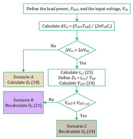
Figure 9.
Flowchart of the operation scenario selection for the converter in the boost-SRC conditions.
3. Experimental Validation
3.1. Design Guidelines
3.1.1. Transformer
The transformer should be designed at the nominal input voltage, , which should correspond to the most probable operating point of the converter. Therefore, the turns ratio can be selected as in (26) to ensure the converter generates the desired output voltage at Db = 0. Additionally, to reduce the copper loss and the proximity losses in the transformer windings, the Litz wire is preferably utilized where it has a large effective number of layers [9]. The magnetic material of the transformer core is the 3C95 ferrite with an ETD39 core type. This material has a low power loss per volume and is more suitable for low to medium switching frequency applications [18]. The number of turns in the primary winding has to be optimized to avoid saturation of the core at the maximum input voltage (27). Additionally, the window area of the core should be taken into account when calculating the number of turns. After selecting the turn number of the primary winding, the secondary turns can be calculated based on the transformer turns ratio. The primary and secondary layers are preferably separated using an isolation material like Kapton tape to ensure high breakdown voltage of the isolation barrier [19]. This isolation material features a high temperature range as well as high strength [20].
where B is the peak-to-peak flux density in the core, Np is the primary turns, and Ac is the effective cross-section area of the core. The magnetizing inductance shall be dimensioned so that the magnetizing current can fully charge and discharge the parasitic output capacitance of the primary semiconductors during the dead time [15] as:
where TDT is dead time in the gating signals of the primary switches.
3.1.2. Resonance Tank Parameters
The resonance inductance affects the required duty cycle and the root mean square (RMS) value of the currents in the circuit. It needs to be optimized to minimize the losses at the nominal input voltage. The relation between the resonance inductance and the losses in the converter is depicted in Figure 10. The losses model of the semiconductors has been adopted from work in [21], while the core losses are estimated based on the improved generalized Steinmetz equation [22]. It is clear that when increasing the inductance, the losses in the circuit decrease. However, the leakage inductance should be low enough to ensure resonant tank operation with a discontinuous resonant current, i.e., a Q factor less than one. Next, Cr could be selected regarding the target resonance frequency and utilizing the value of Lr. The material of Cr should have a low series resistance and low temperature coefficient as well [13].

Figure 10.
Dependence of the total power loss of the converter (Ploss) on the resonance inductance value.
3.2. Description of the Experimental Testbench
The rated power and the nominal input voltage of the designed converter are 300 W and 30 V, respectively. The turns ratio of the transformer equals six according to (26). The experimental setup photo is given in Figure 11, while the list of the parameters and components utilized in the prototype is given in Table 2. An external inductor is wound to compensate for the low value of Llk of the transformer. The resonance frequency of the converter is 92.3 kHz, which is close to the switching frequency to improve the converter efficiency. All efficiency measurements were taken with the Yokogawa WT1800 precision power analyzer, with the exception of the auxiliary power consumption. The control system is implemented utilizing the low-cost STM32F334 microprocessor.

Figure 11.
Experimental setup in the laboratory.
Table 2.
Setup parameters and components.
3.3. DC Voltage Gain
Figure 12 shows the theoretical and experimental gain versus the boosting duty cycle Db at different loading powers. The output voltage to input voltage ratio is referred to as the dc voltage gain, G = VOUT/VIN. The duty cycle represents only the boosting interval in the positive half-cycle of the switch Q. It can be noted that the two curves are approximately matched with a small deviation as the mathematical analysis is done for the lossless system. Furthermore, at the same dc voltage gain G, the power level influences the duty cycle value. Larger deviations between the theoretical and experimental gain curves observed at lower powers can be explained by the effect of the parasitic capacitances of the output-side semiconductors.

Figure 12.
Theoretical and experimental dc voltage gain curves versus the boosting duty cycle Db.
3.4. Measured Efficiency
The efficiency is measured in the pure-SRC conditions at 30 V and boost-SRC conditions at 25 V, as shown in Figure 13. The efficiency of pure-SRC is higher than at 25 V for most of the power levels due to negligible switching power losses. The peak efficiency of pure-SRC and 25 V equals 96.5% and 96%, respectively. The weighted California Energy Commission (CEC) efficiency equals 94.4% and 95.8% for the boost-SRC and pure-SRC conditions, respectively. At lower powers, the controllability is decreased as a smaller duty cycle Db is needed to regulate the input voltage.

Figure 13.
Measured efficiency of the proposed converter at the nominal input voltage of 30 V and in the boost-SRC at 25 V.
3.5. Comparison with the Existing Topology with an AC-Switch
The proposed topology is considered a modification of the baseline topology shown in Figure 14 [17]. The latter comprises two switches and two diodes to boost the input voltage, implementing the ac-switch-based technique, i.e., using a bidirectional switch. The range of the input voltage that the two converters can regulate is measured in the laboratory, as shown in Figure 15a. It can be noted that the proposed topology covers a wider range than that of the topology in [17]. As can be observed from the figure, the proposed converter can regulate the input voltage and power in a wider range compared to the circuit based on the ac-switch. Next, the efficiency of both circuits was measured versus the power level, as shown in Figure 15b. It is worth noting that in pure-SRC conditions, all topologies work the same at the nominal voltage. The proposed topology provides slightly lower efficiency in the boost-SRC conditions at 25 V, which, however, is a justifiable disadvantage considering the improved converter regulation range.

Figure 14.
SRC configuration based on the ac-switch boosting technique [17].
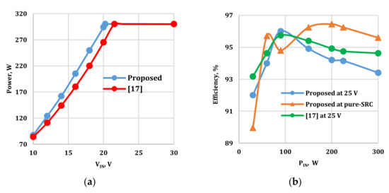
Figure 15.
Comparison between the proposed topology and the topology in [17]: (a) Measured operating range and (b) measured efficiency.
3.6. Steady-State Waveforms
3.6.1. Pure-SRC Conditions
The experimental results for the trajectory curve and the steady-state waveforms are shown in Figure 16 and Figure 17, respectively. The operating power of the converter was 200 W. The radius of the bottom half-circle in the state trajectory is 210 V, which refers to the peak-to-peak ripple of the resonant capacitor voltage, and the theoretical value of ∆VCr equals 198.5 V. In the negative half-cycle, the secondary winding (resonant) current follows the half-wave sinusoidal shape with a peak value of 1.85 A. The resonant capacitor discharges from the value of 285 V down to 75 V at the end of this half-cycle. At the end of the positive half-cycle, the converter operates in the freewheeling condition for a short time.

Figure 16.
Measured state–space trajectory curve in the pure-SRC conditions.

Figure 17.
Steady-state waveforms of the converter in the pure-SRC conditions: (a) At the input and (b) output sides.
3.6.2. Boost-SRC, Scenario A
The trajectory curve and the steady-state waveforms are shown in Figure 18. In this case, the input voltage and the converter power equal 25 V and 200 W, respectively. The measured value of ∆VCr is 232 V, which matches the theoretical prediction of 234 V calculated from (2). The boosting duty cycle Db equals 0.055. The value of the secondary current, ITX,sec, at the end of the boosting interval is 2.8 A. The converter operation corresponds to the theoretical analysis. As the resonant current decreases to zero, parasitic voltage oscillations are generated by parasitic capacitances of the output-side semiconductors, but this has little effect on the converter’s main operating principle.
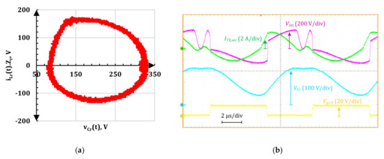
Figure 18.
Experimental waveform of the proposed converter for scenario A: (a) Trajectory curve and (b) steady-state waveforms.
3.6.3. Boost-SRC, Scenario B
During this case, the input voltage and the power level are 20 V and 200 W, respectively. The experimental results for the trajectory curve and the steady-state waveforms are shown in Figure 19. The boosting duty cycle Db equals 0.15. It is clear that the converter has a single-boosting mode as the capacitor continues charging while the resonance inductor is discharging in the positive half-cycle. Further, the capacitor voltage in the negative half-cycle starts discharging from the output voltage of 350 V down to 105 V at the end of the half-cycle. This change in the voltage VCr represents the peak-to-peak ripple, which matches the theoretical value at 2nVIN, i.e., 240 V. During the boosting interval, the inductor current charges according to the sinusoidal law up to approximately 5 A, then it begins to discharge until the resonant current drops to zero. It is worth mentioning that the resonant capacitor voltage reaches the output voltage level soon after the boosting interval is finished and remains unchanged till the end of the half-cycle.

Figure 19.
Experimental waveform of the proposed converter for scenario B: (a) Trajectory curve and (b) steady-state waveforms.
3.6.4. Boost-SRC, Scenario C
During this case, the input voltage is set to 17 V, the converter power equals 200 W, while the boosting duty cycle Db equals 0.15. The experimental result of the trajectory curve is shown in Figure 20a, and the obtained shape matches the theoretical one in Figure 5c. The capacitor voltage reaches the output voltage before ending the boosting interval, as shown in Figure 20b. The secondary winding current changes according to the sinusoidal law before the instant when vCr(t) = VOUT, and linearly after that. The theoretical and measured values of ∆VCr are 204 V and 205 V, respectively. The two values are well matched, which confirms the validity of the circuit analysis in this case.

Figure 20.
Experimental waveform of the proposed converter for scenario C: (a) Trajectory curve, and (b) steady-state waveforms.
A simple closed-loop control system is designed to generate the duty cycle that will regulate the output voltage at its reference point, as shown in Figure 21. When a maximum is hit, the anti-windup feedback limits the input of the integrator, preventing a significant value of integrating action. The proportional and integral gains of the proportional-integral (PI) regulator are 0.23 and 0.001, respectively. The system is tested in two conditions to ensure the robustness of the designed regulator. First, the load resistance is changed in a step from 1000 Ω to 500 Ω, i.e., the power is changed from 122.5 W to 245 W. The output voltage remains constant at 350 V, as shown in Figure 22a. The input voltage during this test equals 25 V, and the input current increases from 5.5 A to 11.3 A, corresponding to the load step. Additionally, ∆VCr changes with the power level, which agrees with the theoretical prediction (2).

Figure 21.
Block diagram of the closed-loop system using the PI regulator with an anti-windup strategy.

Figure 22.
The converter response to (a) load step change and (b) the input voltage ramp.
The next test is done by ramping the input voltage from 25 V down to 15 V within 0.5 s, while the load resistance equals 1000 Ω. The response of the converter output voltage is shown in Figure 22b. The converter operates in the boost-SRC condition and switches between all three operation scenarios during this input voltage change.
The resonant capacitor voltage stress constraint on the output voltage is a significant advantage of the proposed converter. It is known that resonant capacitors are prone to failure in galvanically isolated dc-dc converters [23]. In other existing topologies, including the single form [17], the resonant capacitor could experience much higher voltage stress during transients due to resonant current overshoots, which is avoided in the proposed converter.
4. Conclusions
The paper has introduced a new topology of the series resonant dc-dc converter with galvanic isolation and discontinuous resonant current. This topology utilizes a novel boosting rectifier cell with one MOSFET, two diodes, and two capacitors at the high voltage side. It employs the converter resonant inductor as a boost inductor for voltage boost. Compared to its counterparts based on a voltage doubler rectifier, this boosting cell reduces the number of semiconductor components and clamps the resonant capacitor voltage to the maximum output voltage. The latter feature ensures safe converter operation under any regulation transients when connected to a stable dc microgrid, but it provides slightly lower efficiency compared to the closest existing SRC-based topology with an ac-switch. Nevertheless, the proposed converter can achieve the soft switching feature, and the maximum efficiency of the converter was 96.5%. The obtained features enable using the proposed converter in distributed generation applications where it needs to operate in a wide range of input voltage and power.
Author Contributions
Conceptualization, A.B. (Abualkasim Bakeer) and A.C.; methodology, A.B. (Abualkasim Bakeer), A.C., and J.-S.L.; software, A.B. (Abualkasim Bakeer); validation, A.C. and A.B. (Andrei Blinov); formal analysis, A.B. (Abualkasim Bakeer); investigation, A.B. (Abualkasim Bakeer); resources, A.C.; data curation, A.B. (Andrei Blinov); writing—original draft preparation, A.C. and A.B. (Abualkasim Bakeer); writing—review and editing, A.B. (Abualkasim Bakeer), A.B. (Andrei Blinov), and J.-S.L.; visualization, A.B. (Abualkasim Bakeer) and A.B. (Andrei Blinov); supervision, A.C.; project administration, A.C.; funding acquisition, A.C. All authors have read and agreed to the published version of the manuscript.
Funding
This research was supported in part by the Estonian Research Council grant PSG206, and in part by the Estonian Centre of Excellence in Zero Energy and Resource Efficient Smart Buildings and Districts, ZEBE, grant 2014-2020.4.01.15-0016 funded by the European Regional Development Fund.
Institutional Review Board Statement
Not applicable.
Informed Consent Statement
Not applicable.
Data Availability Statement
Not applicable.
Conflicts of Interest
The authors declare no conflict of interest.
Nomenclature
| PV | Photovoltaic |
| SRC | Series resonant converter |
| ZVS | Zero voltage switching |
| LLC | Inductor-inductor-capacitor resonant converter |
| MOSFET | Metal oxide semiconductor field-effect transistor |
| Cr | Resonant capacitance (F) |
| Fr | Resonant frequency (Hz) |
| FSW | Switching frequency (Hz) |
| Lr | Resonant inductance (H) |
| Llk | Leakage inductance (H) |
| Lext | External inductance (H) |
| VCr | The average voltage of the resonant capacitor (V) |
| VOUT | Output voltage (V) |
| Lm | The magnetizing inductance of the transformer (H) |
| n | Turns ratio of the transformer |
| Coss | Parasitic output capacitance of the input-side bridge semiconductors |
| Db | Cumulative boosting duty cycle |
| TSW | Switching period (s) |
| POUT | Output power (W) |
| ΔVCr | The peak-to-peak ripple of the resonant capacitor voltage |
| VIN | Input voltage (V) |
| CO | Output capacitance (F) |
| Zr | Resonant impedance (Ω) |
| ZCS | Zero current switching |
| ωr | Angular resonant frequency (rad/s) |
| β | Initial angle (rad) |
| DCM | Discontinuous conduction mode |
| G | Normalized dc voltage gain |
| PIN | Input power (W) |
| B | Peak-to-peak flux density of the transformer (Weber/m2) |
| Np | Number of the primary winding turns |
| Ac | Effective core area (m2) |
| TDT | Dead-time between the two MOSFETs in the input-side bridge (s) |
| tcri | Critical time to charge the resonance capacitor into the output voltage (s) |
| VOUT_ref | Reference of the output voltage |
References
- Comello, S.; Reichelstein, S.; Sahoo, A. The Road Ahead for Solar PV Power. Renew. Sustain. Energy Rev. 2018, 92, 744–756. [Google Scholar] [CrossRef]
- Zubieta, L.E. Are Microgrids the Future of Energy?: DC Microgrids from Concept to Demonstration to Deployment. IEEE Electrif. Mag. 2016, 4, 37–44. [Google Scholar] [CrossRef]
- Vinnikov, D.; Chub, A.; Liivik, E.; Kosenko, R.; Korkh, O. Solar Optiverter—A Novel Hybrid Approach to the Photovoltaic Module Level Power Electronics. IEEE Trans. Ind. Electron. 2019, 66, 3869–3880. [Google Scholar] [CrossRef]
- Li, C.; Wang, H. A Wide Gain Range LLC Resonant Converter Based on Reconfigurable Bridge and Asymmetric Resonant Tanks. In Proceedings of the 2019 IEEE Applied Power Electronics Conference and Exposition (APEC), Anaheim, CA, USA, 17–21 March 2019. [Google Scholar] [CrossRef]
- Hsieh, H.-I.; Wang, H.; Huang, T.-H. LLC Charger Using Quasi-Contactless Power Transfer by Resonant Magnetic Induction Coupling. IEEE Trans. Transp. Electrif. 2018, 4, 376–388. [Google Scholar] [CrossRef]
- Yi, K.-H.; Moon, G.-W. Novel Two-Phase Interleaved LLC Series-Resonant Converter Using a Phase of the Resonant Capacitor. IEEE Trans. Ind. Electron. 2009, 56, 1815–1819. [Google Scholar] [CrossRef]
- Wu, H.; Zhang, J.; Qin, X.; Mu, T.; Xing, Y. Secondary-Side-Regulated Soft-Switching Full-Bridge Three-Port Converter Based on Bridgeless Boost Rectifier and Bidirectional Converter For Multiple Energy Interface. IEEE Trans. Power Electron. 2015, 1. [Google Scholar] [CrossRef]
- Son, S.; Montes, O.A.; Junyent-Ferre, A.; Kim, M. High Step-Up Resonant DC/DC Converter With Balanced Capacitor Voltage for Distributed Generation Systems. IEEE Trans. Power Electron. 2019, 34, 4375–4387. [Google Scholar] [CrossRef]
- Jang, S.R.; Ryoo, H.J.; Kim, J.S.; Ahn, S.H. Design and Analysis of Series Resonant Converter for 30 kW Industrial Magnetron. In Proceedings of the IECON 2010—36th Annual Conference on IEEE Industrial Electronics Society, Glendale, AZ, USA, 7–10 November 2010. [Google Scholar] [CrossRef]
- Sidorov, V.; Chub, A.; Vinnikov, D.; Bakeer, A. An Overview and Comprehensive Comparative Evaluation of Constant-Frequency Voltage Buck Control Methods for Series Resonant DC–DC Converters. IEEE Open J. Ind. Electron. Soc. 2021, 2, 65–79. [Google Scholar] [CrossRef]
- Bakeer, A.; Chub, A.; Vinnikov, D.; Rosin, A. Wide Input Voltage Range Operation of the Series Resonant DC-DC Converter with Bridgeless Boost Rectifier. Energies 2020, 13, 4220. [Google Scholar] [CrossRef]
- Bakeer, A.; Chub, A.; Vinnikov, D. Step-Up Series Resonant DC–DC Converter with Bidirectional-Switch-Based Boost Rectifier for Wide Input Voltage Range Photovoltaic Applications. Energies 2020, 13, 3747. [Google Scholar] [CrossRef]
- Zhao, X.; Zhang, L.; Born, R.; Lai, J.-S. A High-Efficiency Hybrid Resonant Converter With Wide-Input Regulation for Photovoltaic Applications. IEEE Trans. Ind. Electron. 2017, 64, 3684–3695. [Google Scholar] [CrossRef]
- Kim, S.; Kim, B.; Kwon, B.-H.; Kim, M. An Active Voltage-Doubler Rectifier Based Hybrid Resonant DC/DC Converter for Wide-Input-Range Thermoelectric Power Generation. IEEE Trans. Power Electron. 2018, 33, 9470–9481. [Google Scholar] [CrossRef]
- Zhao, X.; Chen, C.-W.; Lai, J.-S. A High-Efficiency Active-Boost-Rectifier-Based Converter With a Novel Double-Pulse Duty Cycle Modulation for PV to DC Microgrid Applications. IEEE Trans. Power Electron. 2019, 34, 7462–7473. [Google Scholar] [CrossRef]
- Kim, J.-W.; Park, M.-H.; Han, J.-K.; Lee, M.; Lai, J.-S. PWM Resonant Converter With Asymmetric Modulation for ZVS Active Voltage Doubler Rectifier and Forced Half Resonance in PV Application. IEEE Trans. Power Electron. 2020, 35, 508–521. [Google Scholar] [CrossRef]
- LaBella, T.; Yu, W.; Lai, J.-S.; Senesky, M.; Anderson, D. A Bidirectional-Switch-Based Wide-Input Range High-Efficiency Isolated Resonant Converter for Photovoltaic Applications. IEEE Trans. Power Electron. 2014, 29, 3473–3484. [Google Scholar] [CrossRef]
- Material Specification of 3C95. Available online: https://www.ferroxcube.com/upload/media/product/file/MDS/3c95.pdf (accessed on 1 July 2020).
- Shen, Z.; Wang, H.; Shen, Y.; Qin, Z.; Blaabjerg, F. Winding Design of Series AC Inductor for Dual Active Bridge Converters. In Proceedings of the 2018 IEEE Applied Power Electronics Conference and Exposition (APEC), San Antonio, TX, USA, 4–8 March 2018. [Google Scholar] [CrossRef]
- Technical Datasheet of Kapton Polyimide Film Type. Available online: https://www.emsdiasum.com/microscopy/technical/datasheet/77708.aspx (accessed on 1 July 2020).
- Graovac, D.; Purschel, M.; Kiep, A. MOSFET power losses calculation using the data-sheet parameters. Infineon Appl. Note 2006, 1, 1–23. [Google Scholar]
- Venkatachalam, K.; Sullivan, C.R.; Abdallah, T.; Tacca, H. Accurate Prediction of Ferrite Core Loss with Nonsinusoidal Waveforms Using Only Steinmetz Parameters. In Proceedings of the 2002 IEEE Workshop on Computers in Power Electronics, Mayaguez, PR, USA, 3–4 June 2002. [Google Scholar] [CrossRef]
- Ferreira Costa, L.; Liserre, M. Failure Analysis of the Dc-Dc Converter: A Comprehensive Survey of Faults and Solutions for Improving Reliability. IEEE Power Electron. Mag. 2018, 5, 42–51. [Google Scholar] [CrossRef]


Publisher’s Note: MDPI stays neutral with regard to jurisdictional claims in published maps and institutional affiliations. |
© 2021 by the authors. Licensee MDPI, Basel, Switzerland. This article is an open access article distributed under the terms and conditions of the Creative Commons Attribution (CC BY) license (https://creativecommons.org/licenses/by/4.0/).