
A GaN-HEMT Compact Model Including Dynamic RDSon Effect for Power Electronics Converters

 , , , and
Abstract
:1. Introduction
- (1)
- This compact model is integrated into our developed Power Electronics Virtual Prototyping (PEVP) design tool, which takes consideration of electrical circuit EM analysis by PEEC method. In comparison with the above-discussed approaches, one advantage is that it is applied model order reduction (MOR) for PEEC method, which is able to reduce the numbers of equations for EM analysis so as to obtain device switching transients in the range of minutes. It helps designers to save simulation time as discussed above.
- (2)
- The compact model also includes device dynamic values, which can be applied into different circuit simulators for power electronics converters. It helps designers to accurately obtain device losses in simulation as most GaN-HEMT model do not include dynamic effect for power electronics converters.
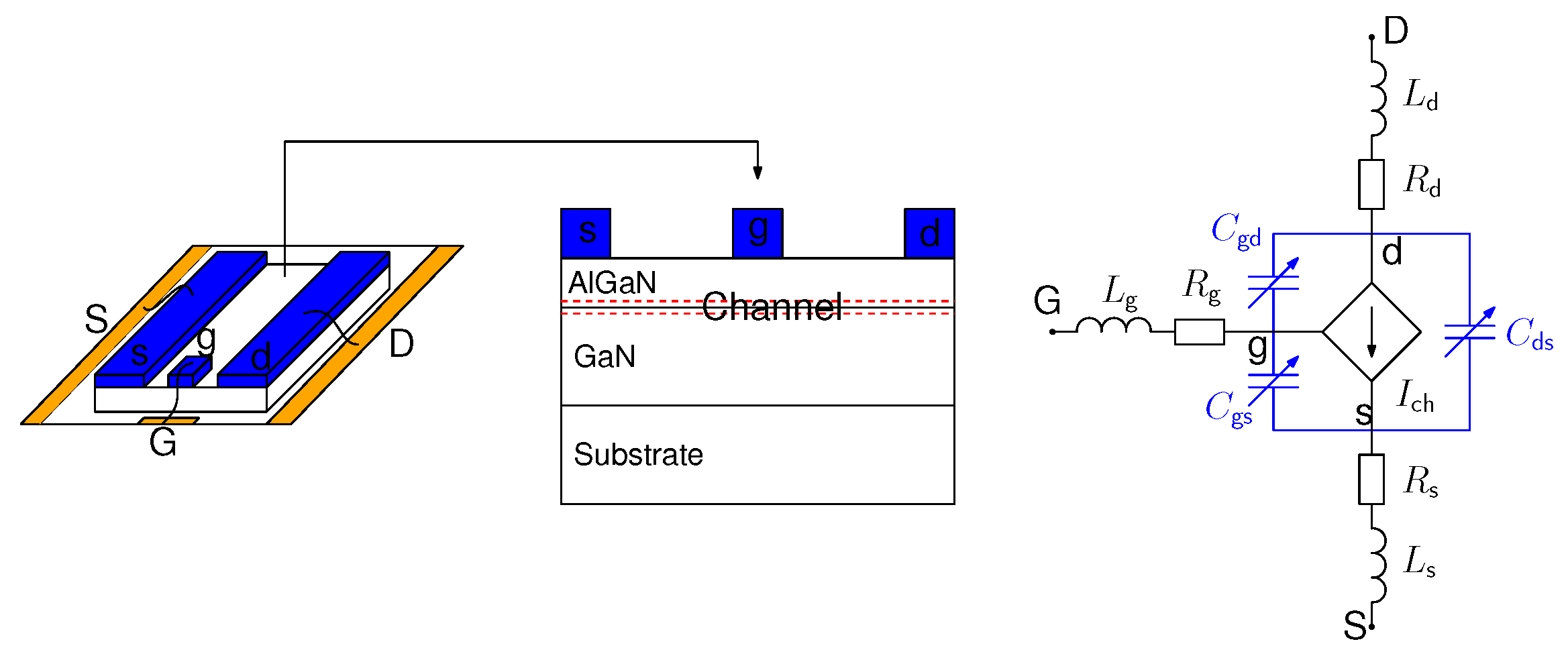
2. GaN-HEMT Compact Model
2.1. Model Principle
2.2. Model Implementation into Power Electronics Virtual Prototyping Software
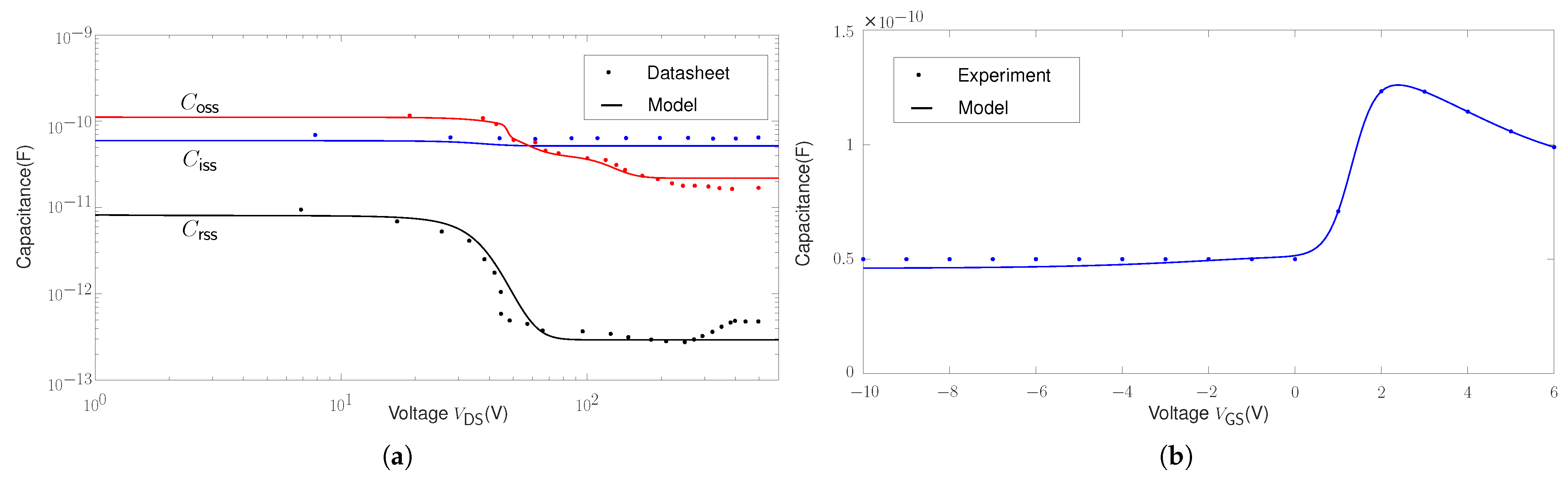
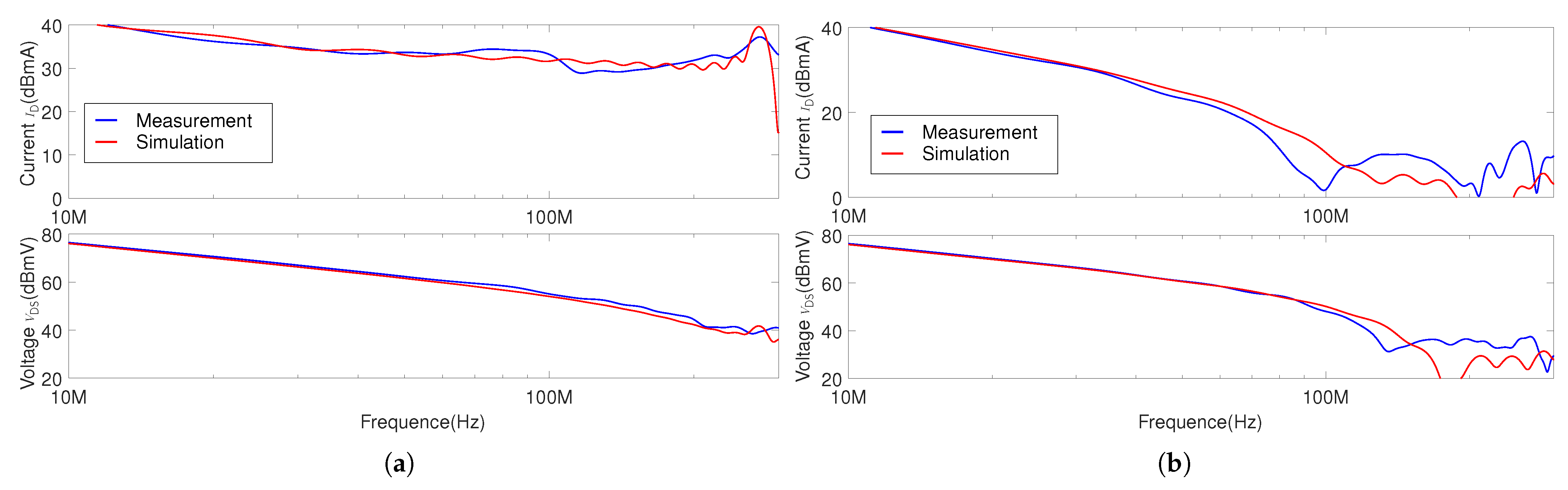
2.3. Model Validation
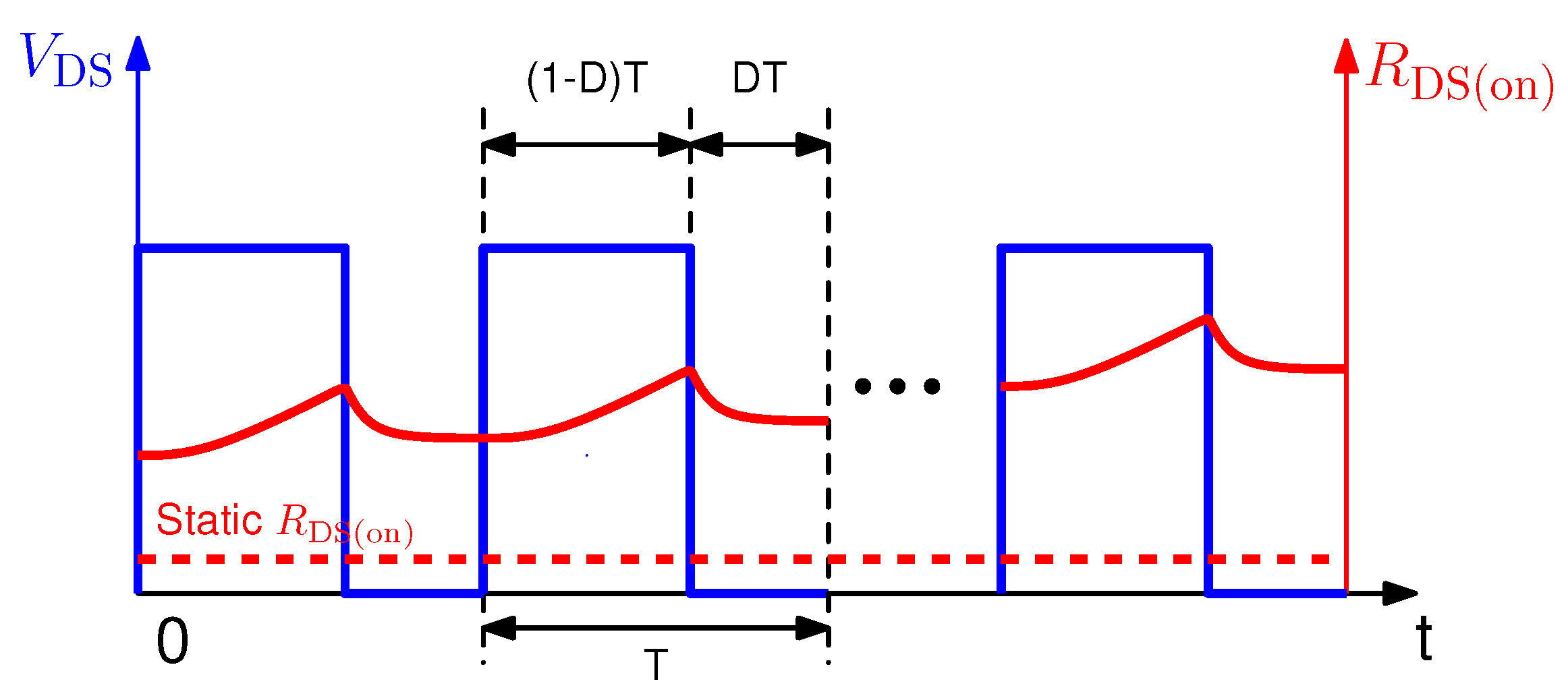
3. GaN-HEMT Dynamic Compact Model
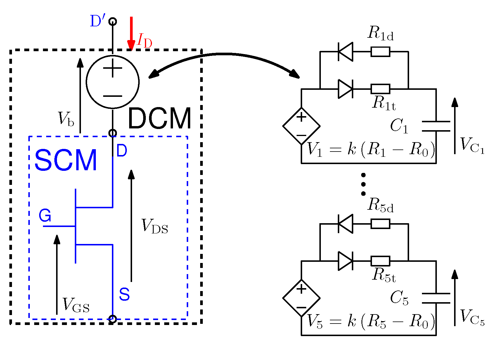
3.1. Model Principle and Parameters Extraction
3.2. Model Implementation
3.3. Model Validation
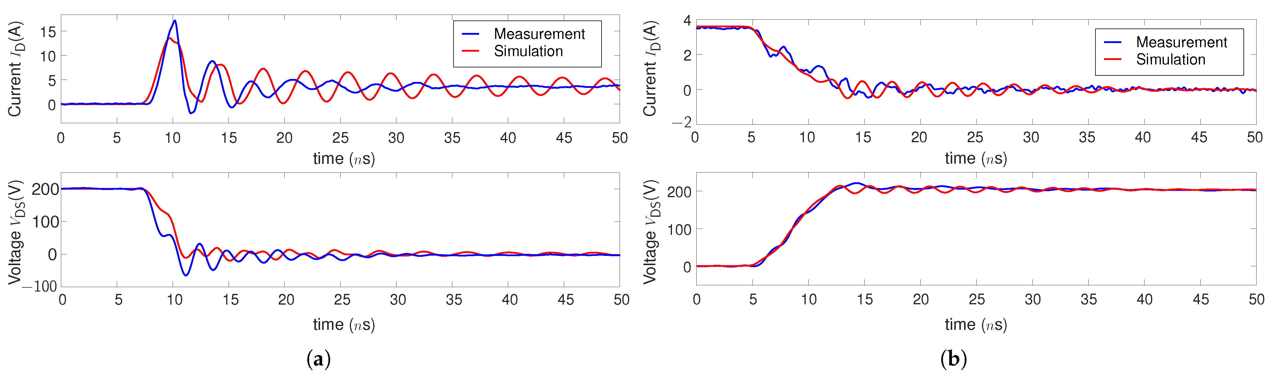
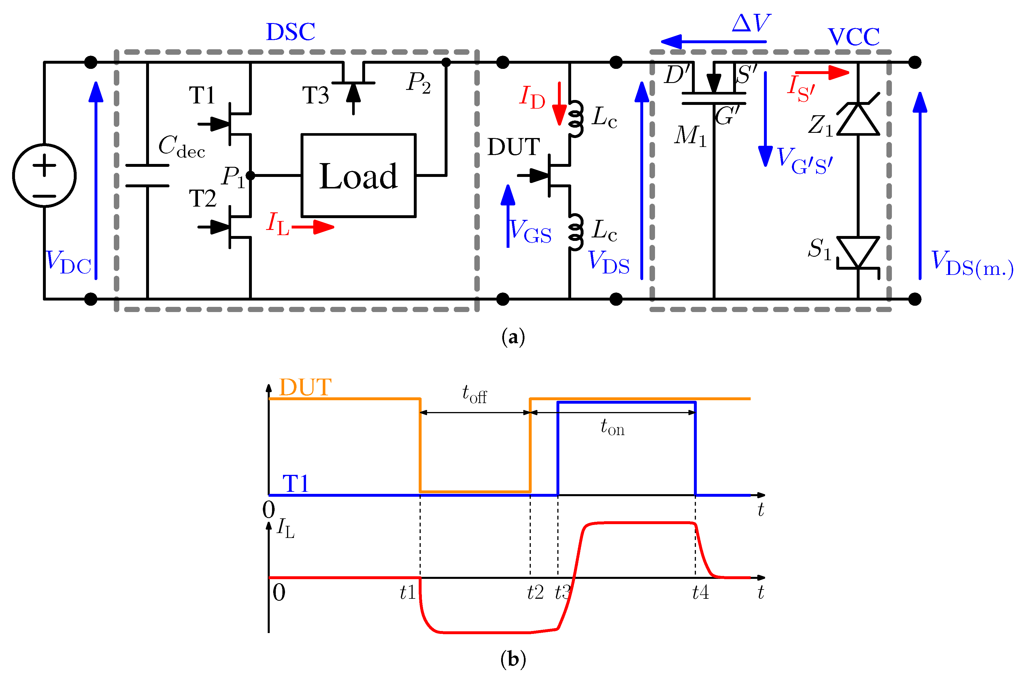
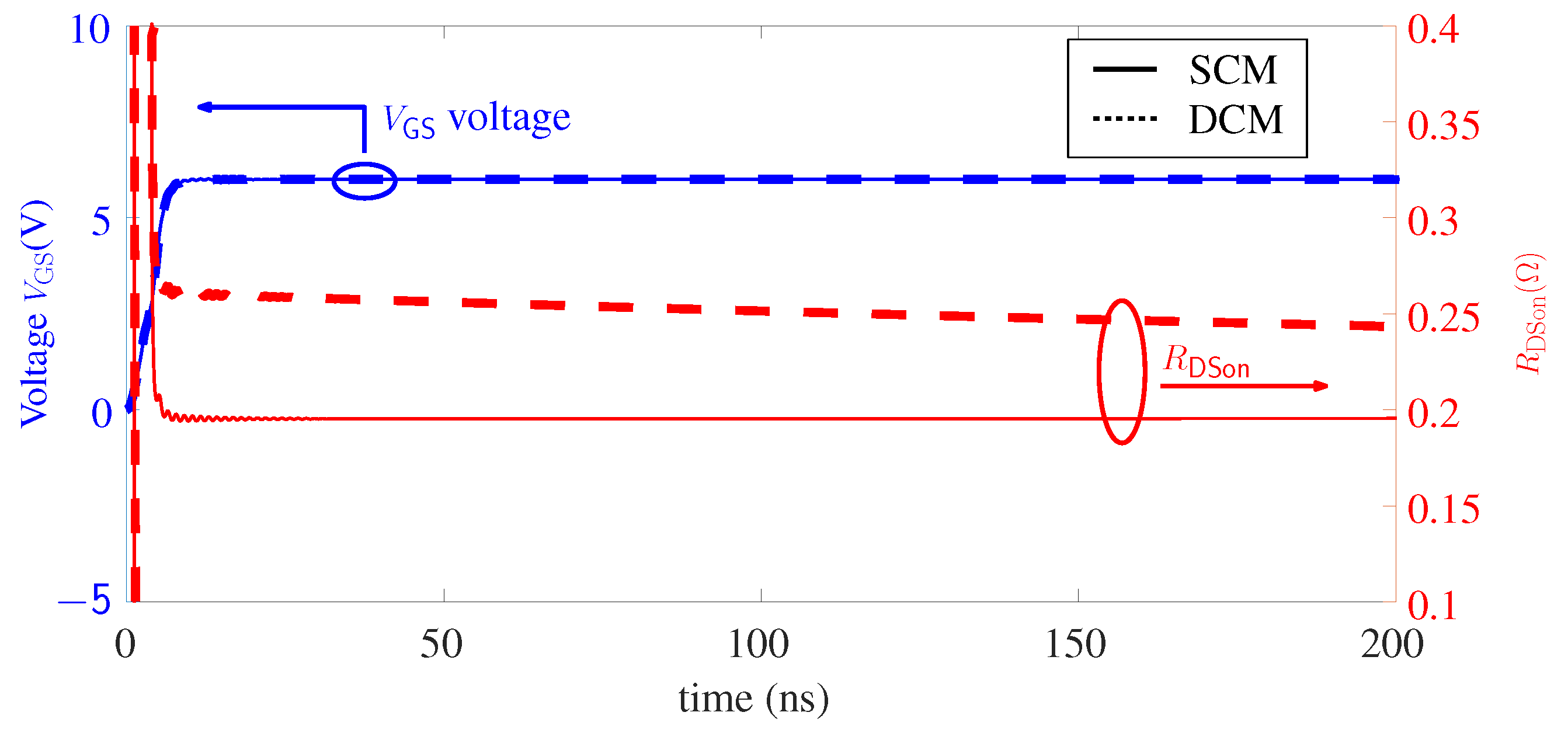
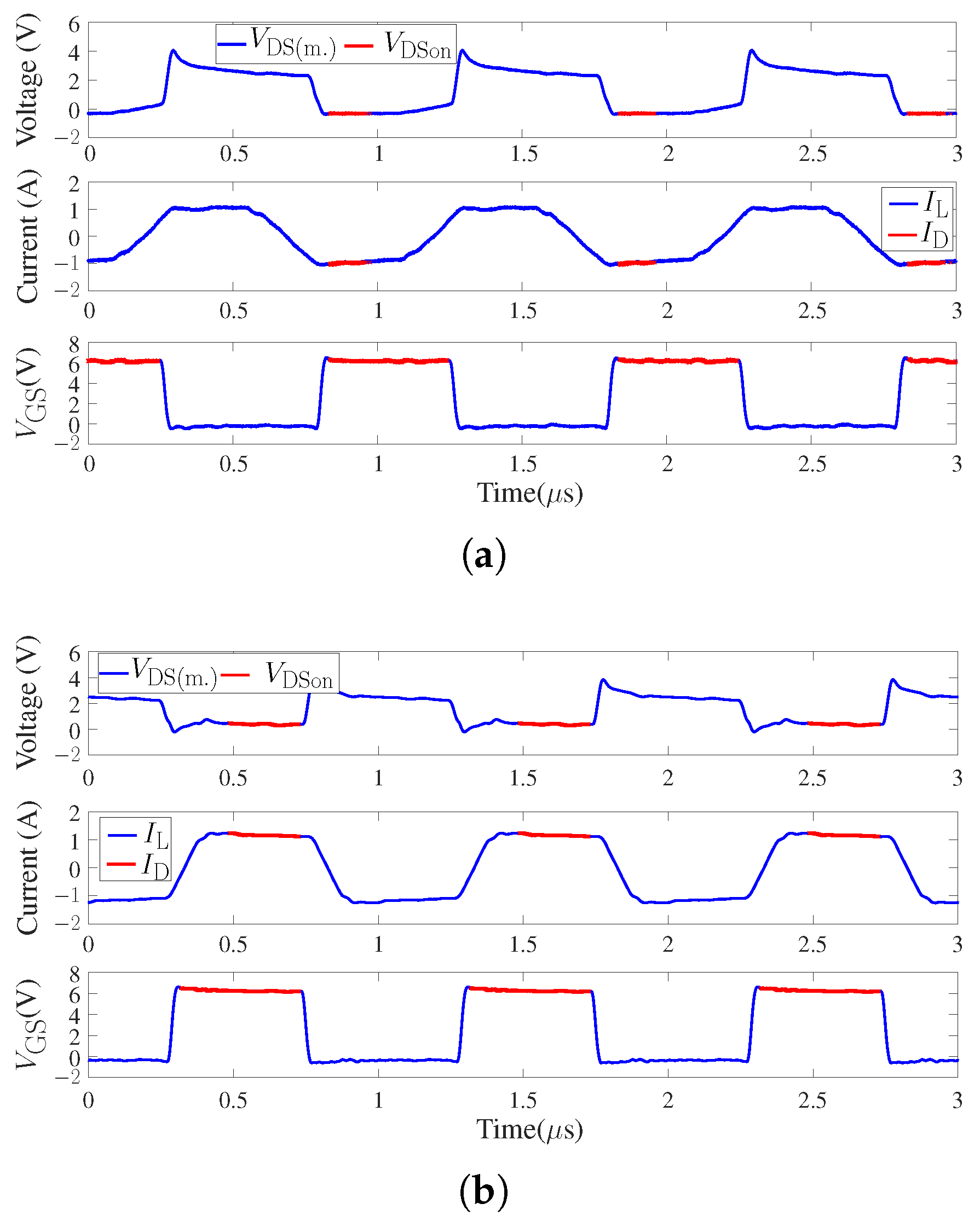
3.3.1. Transient and Steady State
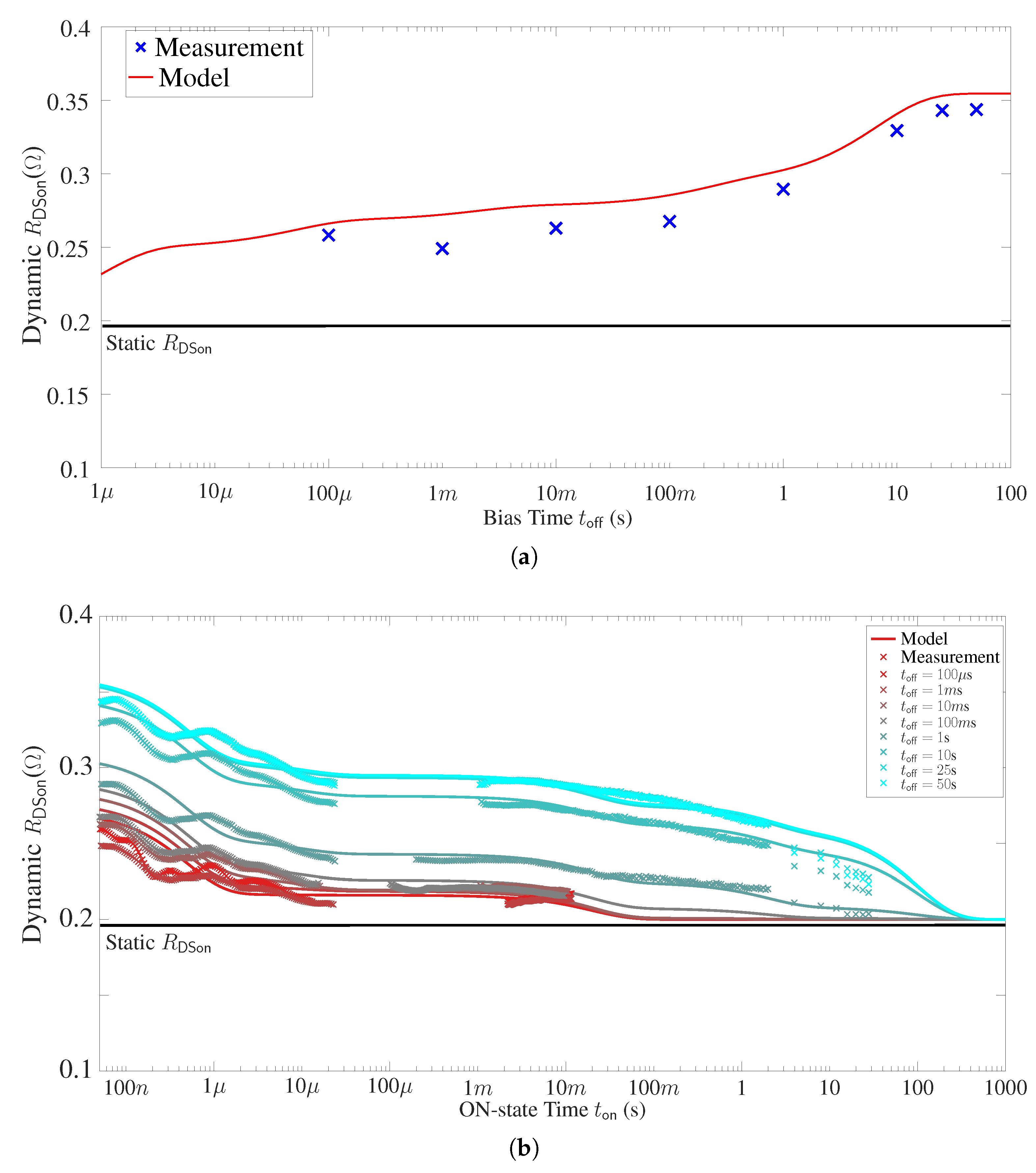
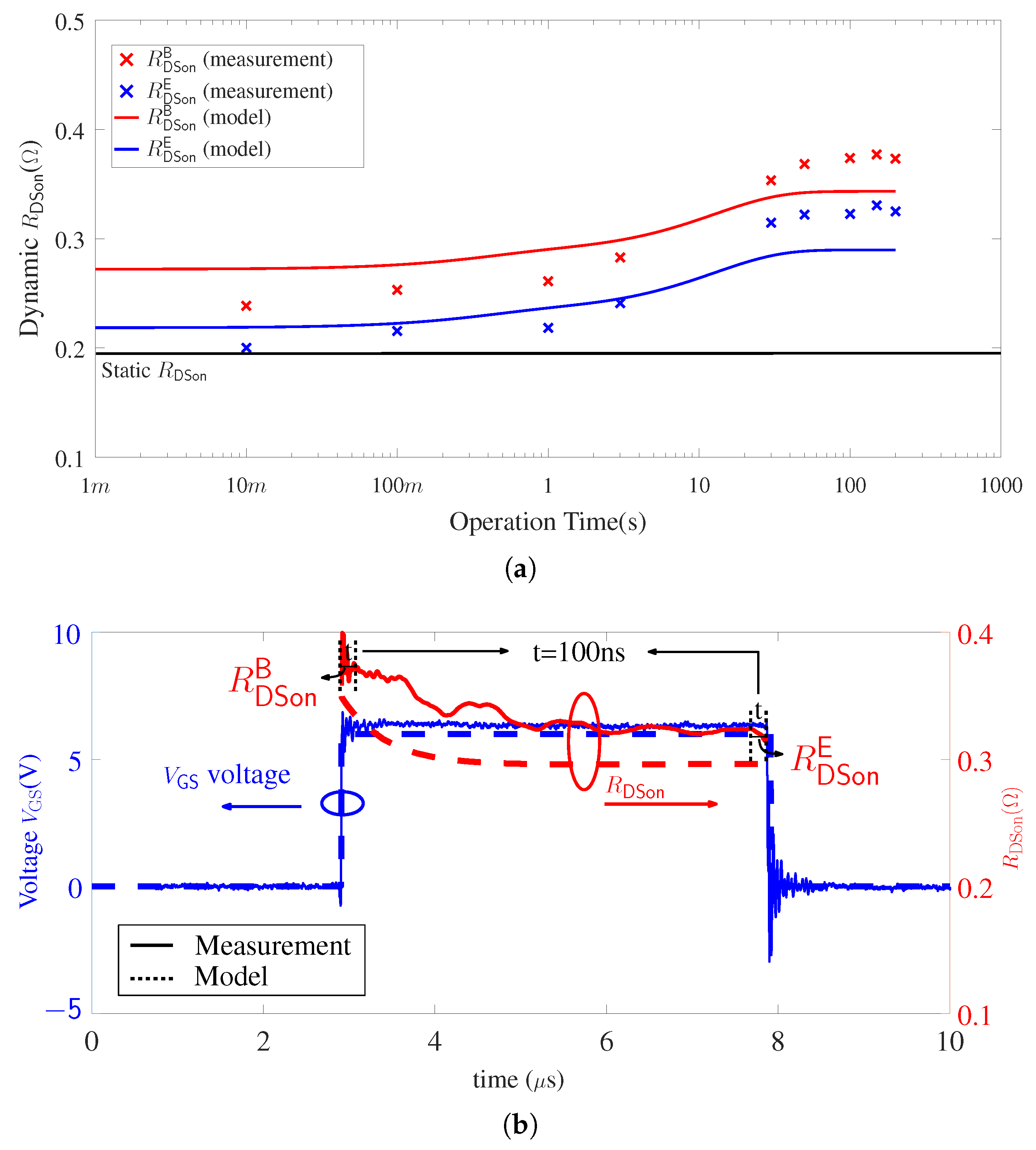
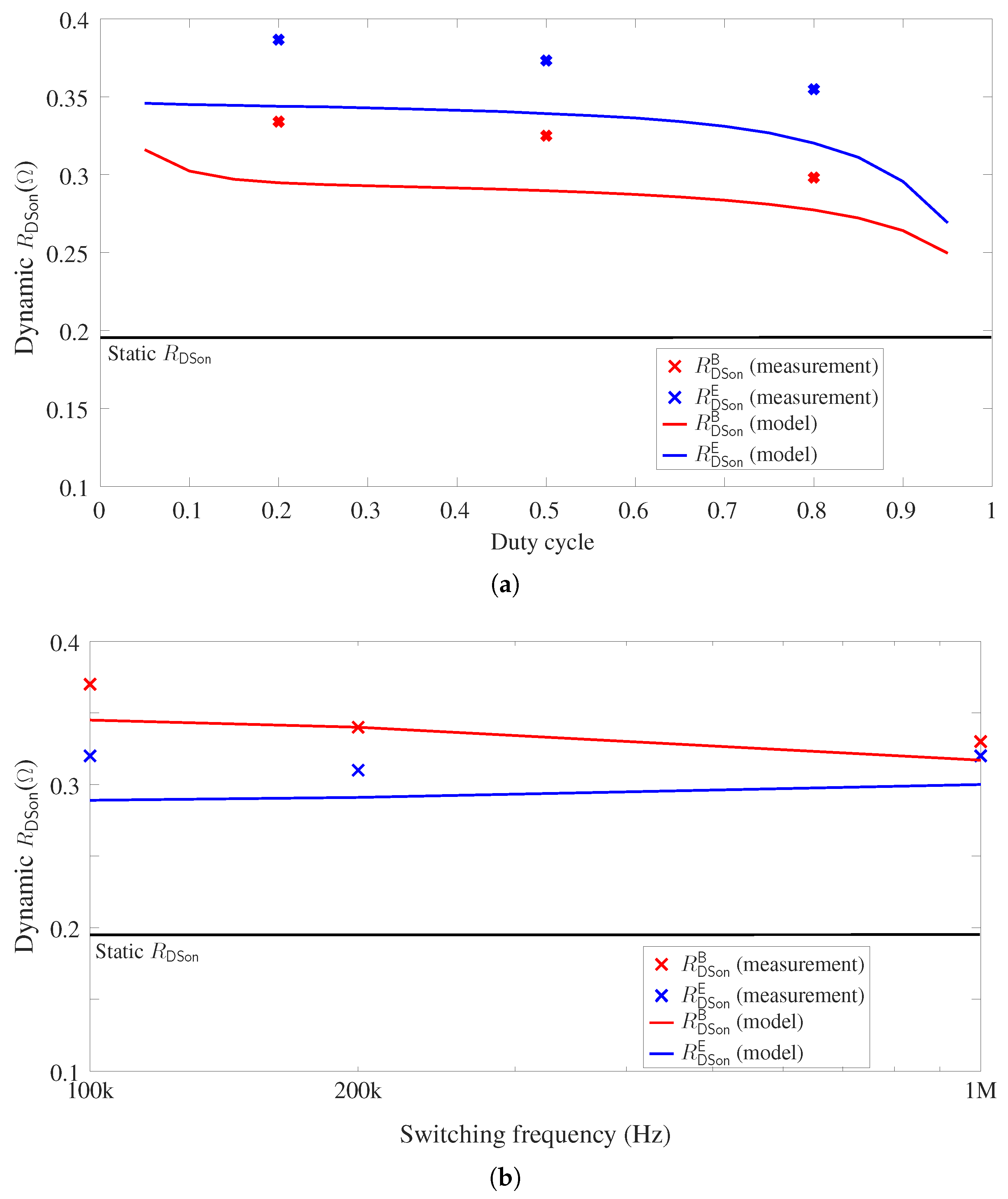
3.3.2. Different Operation Conditions
3.3.3. Discussion
4. Conclusions
Author Contributions
Funding
Acknowledgments
Conflicts of Interest
Abbreviations
| GaN | Gallium Nitride |
| HEMT | High Electron Mobility Transistors |
| SiC | Silicon Carbide |
| PFC | Power Factor Correction |
| FEM | Finite Element Method |
| PEEC | Partial Element Equivalent Circuit |
| EM | Electromagnetic |
| MOR | Model Order Reduction |
| PEVP | Power Electronics Virtual Prototyping |
| ZVS | Zero Voltage Soft Switching |
| DUT | Device Under Test |
| PCB | Printed Circuit Board |
| DCM | GaN-HEMT Dynamic Compact Model |
| SCM | Standard GaN-HEMT Compact Model |
References
- Fu, M.; Fei, C.; Yang, Y.; Li, Q.; Lee, F.C. A GaN-Based DC–DC Module for Railway Applications: Design Consideration and High-Frequency Digital Control. IEEE Trans. Ind. Electron. 2020, 67, 1638–1647. [Google Scholar] [CrossRef]
- Shin, J.; Ishigaki, M.; Dede, E.M.; Lee, J.S. MagCap DC–DC Converter Utilizing GaN Devices: Design Consideration and Quasi-Resonant Operation. IEEE Trans. Power Electron. 2019, 34, 2441–2453. [Google Scholar] [CrossRef]
- Li, X.; Ma, H.; Yi, J.; Lu, S.; Xu, J. A Comparative Study of GaN HEMT and Si MOSFET-Based Active Clamp Forward Converters. Energies 2020, 13, 4160. [Google Scholar] [CrossRef]
- Ma, C.T.; Gu, Z.H. Review of GaN HEMT Applications in Power Converters over 500 W. Electronics 2019, 8, 1401. [Google Scholar] [CrossRef] [Green Version]
- Li, K.; Evans, P.; Johnson, M. SiC/GaN power semiconductor devices: A theoretical comparison and experimental evaluation under different switching conditions. IET Electr. Syst. Transp. 2018, 8, 3–11. [Google Scholar] [CrossRef] [Green Version]
- Li, K.; Evans, P.; Johnson, M. Developing Power Semiconductor Device Model for Virtual Prototyping of Power Electronics Systems. In Proceedings of the 2016 IEEE Vehicle Power and Propulsion Conference (VPPC), Hangzhou, China, 17–20 October 2016; pp. 1–6. [Google Scholar] [CrossRef]
- Liu, Z.; Huang, X.; Lee, F.; Li, Q. Package Parasitic Inductance Extraction and Simulation Model Development for the High-Voltage Cascode GaN HEMT. Power Electron. IEEE Trans. 2014, 29, 1977–1985. [Google Scholar] [CrossRef]
- Endruschat, A.; Novak, C.; Gerstner, H.; Heckel, T.; Joffe, C.; März, M. A Universal SPICE Field-Effect Transistor Model Applied on SiC and GaN Transistors. IEEE Trans. Power Electron. 2019, 34, 9131–9145. [Google Scholar] [CrossRef]
- Liang, M.; Zheng, T.Q.; Li, Y. An Improved Analytical Model for Predicting the Switching Performance of SiC MOSFETs. J. Power Electron. 2016, 16, 374–387. [Google Scholar] [CrossRef] [Green Version]
- Pace, L.; Chevalier, F.; Videt, A.; Defrance, N.; Idir, N.; De Jaeger, J.C. Electrothermal Modeling of GaN Power Transistor for High Frequency Power Converter Design. In Proceedings of the 2020 22nd European Conference on Power Electronics and Applications (EPE’20 ECCE Europe), Virtual, Lyon, France, 7–11 September 2020; pp. 1–10. [Google Scholar] [CrossRef]
- Cai, Y.; Forsyth, A.J.; Todd, R. Impact of GaN HEMT dynamic on-state resistance on converter performance. In Proceedings of the 2017 IEEE Applied Power Electronics Conference and Exposition (APEC), Tampa, FL, USA, 26–30 March 2017; pp. 1689–1694. [Google Scholar] [CrossRef]
- Foulkes, T.; Modeer, T.; Pilawa-Podgurski, R.C.N. Developing a standardized method for measuring and quantifying dynamic on-state resistance via a survey of low voltage GaN HEMTs. In Proceedings of the 2018 IEEE Applied Power Electronics Conference and Exposition (APEC), San Antonio, TX, USA, 4–8 March 2018; pp. 2717–2724. [Google Scholar] [CrossRef]
- Badawi, N.; Hilt, O.; Bahat-Treidel, E.; Böcker, J.; Würfl, J.; Dieckerhoff, S. Investigation of the Dynamic On-State Resistance of 600 V Normally-Off and Normally-On GaN HEMTs. IEEE Trans. Ind. Appl. 2016, 52, 4955–4964. [Google Scholar] [CrossRef]
- Yang, F.; Xu, C.; Akin, B. Quantitative Analysis of Different Operating Conditions’ Effect on Dynamic On-Resistance in Enhancement-Mode GaN HEMTs. In Proceedings of the 2018 IEEE 6th Workshop on Wide Bandgap Power Devices and Applications (WiPDA), Atlanta, GA, USA, 31 October–2 November 2018; pp. 134–140. [Google Scholar] [CrossRef]
- Galapon, B.J.; Hanson, A.J.; Perreault, D.J. Measuring Dynamic On Resistance in GaN Transistors at MHz Frequencies. In Proceedings of the 2018 IEEE 19th Workshop on Control and Modeling for Power Electronics (COMPEL), Padua, Italy, 25–28 June 2018; pp. 1–8. [Google Scholar] [CrossRef]
- Lu, B.; Palacios, T.; Risbud, D.; Bahl, S.; Anderson, D. Extraction of Dynamic On-Resistance in GaN Transistors: Under Soft- and Hard-Switching Conditions. In Proceedings of the Compound Semiconductor Integrated Circuit Symposium (CSICS), Waikoloa, HI, USA, 16–19 October 2011; pp. 1–4. [Google Scholar] [CrossRef]
- Li, R.; Wu, X.; Yang, S.; Sheng, K. Dynamic on-State Resistance Test and Evaluation of GaN Power Devices Under Hard- and Soft-Switching Conditions by Double and Multiple Pulses. IEEE Trans. Power Electron. 2019, 34, 1044–1053. [Google Scholar] [CrossRef]
- Uren, M.J.; Karboyan, S.; Chatterjee, I.; Pooth, A.; Moens, P.; Banerjee, A.; Kuball, M. “Leaky Dielectric” Model for the Suppression of Dynamic Ron in Carbon-Doped AlGaN/GaN HEMTs. IEEE Trans. Electron. Devices 2017, 64, 2826–2834. [Google Scholar] [CrossRef] [Green Version]
- Li, K.; Videt, A.; Idir, N.; Evans, P.; Johnson, M. Modelling GaN-HEMT Dynamic ON-state Resistance in High Frequency Power Converter. In Proceedings of the 2020 IEEE Applied Power Electronics Conference and Exposition (APEC), New Orleans, LA, USA, 15–19 March 2020; pp. 1949–1955. [Google Scholar] [CrossRef]
- GaNSystems GS66502B Datasheet REV180420. Available online: https://gansystems.com/wp-content/uploads/2018/04/GS66502B-DS-Rev-180420.pdf (accessed on 5 June 2018).
- Pace, L.; Defrance, N.; Videt, A.; Idir, N.; Dejaeger, J. S-Parameter Characterization of GaN HEMT Power Transistors for High Frequency Modeling. In Proceedings of the PCIM Europe 2018, International Exhibition and Conference for Power Electronics, Intelligent Motion, Renewable Energy and Energy Management, Nuremberg, Germany, 5–7 June 2018; pp. 1–8. [Google Scholar]
- Yeo, H.L.; Tseng, K.J. Modelling technique utilizing modified sigmoid functions for describing power transistor device capacitances applied on GaN HEMT and silicon MOSFET. In Proceedings of the 2016 IEEE Applied Power Electronics Conference and Exposition (APEC), Long Beach, CA, USA, 20–24 March 2016; pp. 3107–3114. [Google Scholar] [CrossRef]
- Jardel, O.; Callet, G.; Charbonniaud, C.; Jacquet, J.C.; Sarazin, N.; Morvan, E.; Aubry, R.; Di Forte Poisson, M.; Teyssier, J.; Piotrowicz, S.; et al. A new nonlinear HEMT model for AlGaN/GaN switch applications. In Proceedings of the 2009 European Microwave Integrated Circuits Conference (EuMIC), Rome, Italy, 28–29 September 2009; pp. 73–76. [Google Scholar]
- Evans, P.; Castellazzi, A.; Johnson, C. Design Tools for Rapid Multidomain Virtual Prototyping of Power Electronic Systems. Power Electron. IEEE Trans. 2016, 31, 2443–2455. [Google Scholar] [CrossRef]
- Li, K.; Evans, P.; Johnson, M. Using multi time-scale electro-thermal simulation approach to evaluate SiC-MOSFET power converter in virtual prototyping design tool. In Proceedings of the 2017 IEEE 18th Workshop on Control and Modeling for Power Electronics (COMPEL), Stanford, CA, USA, 9–12 July 2017; pp. 1–8. [Google Scholar]
- Zulauf, G.; Guacci, M.; Rivas-Davila, J.M.; Kolar, J.W. The Impact of Multi-MHz Switching Frequencies on Dynamic On-Resistance in GaN-on-Si HEMTs. IEEE Open J. Power Electron. 2020, 1, 210–215. [Google Scholar] [CrossRef]
- Yang, S.; Han, S.; Sheng, K.; Chen, K.J. Dynamic On-Resistance in GaN Power Devices: Mechanisms, Characterizations and Modeling. IEEE J. Emerg. Sel. Top. Power Electron. 2019. [Google Scholar] [CrossRef]
- Li, K.; Videt, A.; Idir, N.; Evans, P.L.; Johnson, C.M. Accurate Measurement of Dynamic on-State Resistances of GaN Devices Under Reverse and Forward Conduction in High Frequency Power Converter. IEEE Trans. Power Electron. 2020, 35, 9650–9660. [Google Scholar] [CrossRef]


| a | b1 | b2 | c | d | e | f1 | f2 |
|---|---|---|---|---|---|---|---|
| 1.1837 | 13 | 10.5 | 1.7 | 0.31 | 0.255 | 4.1 | 6.1 |
| n | ||||||||||
|---|---|---|---|---|---|---|---|---|---|---|
| 1 | 131.4 | 42.71 | −1.732 | −1.313 | 690 | 0.2736 | −2.689 | 668 | 0.2712 | −2.598 |
| 2 | 100 | 60.85 | 1.405 | 1.5 | 14.93 | 0.9169 | 5 | 3.933 | 0.07737 | −35 |
| 3 | 103.5 | 9.43 | 0.03019 | −118.9 | 11.49 | 0.7 | −47.34 | 20 | 0.06603 | −51.22 |
| Simulation Software | Simulation Time | ||
|---|---|---|---|
| PEVP | 9.7 nH | 5.4 nH | ∼0.7 min |
| ADS | 9.6 nH | 5.7 nH | ∼100 min |
| Simulation | 3 J | 0.9 J | 3.9 J |
| Measurement | 2.1 J | 0.7 J | 2.8 J |
| (s) | (s) | () | |
|---|---|---|---|
| 1 | 0.255 | ||
| 2 | 0.002 | 0.21 | |
| 3 | 0.02 | 0.2185 | |
| 4 | 0.198 | 2 | 0.2162 |
| 5 | 6.8 | 100 | 0.26 |
Publisher’s Note: MDPI stays neutral with regard to jurisdictional claims in published maps and institutional affiliations. |
© 2021 by the authors. Licensee MDPI, Basel, Switzerland. This article is an open access article distributed under the terms and conditions of the Creative Commons Attribution (CC BY) license (https://creativecommons.org/licenses/by/4.0/).
Share and Cite
Li, K.; Evans, P.L.; Johnson, C.M.; Videt, A.; Idir, N. A GaN-HEMT Compact Model Including Dynamic RDSon Effect for Power Electronics Converters. Energies 2021, 14, 2092. https://doi.org/10.3390/en14082092
Li K, Evans PL, Johnson CM, Videt A, Idir N. A GaN-HEMT Compact Model Including Dynamic RDSon Effect for Power Electronics Converters. Energies. 2021; 14(8):2092. https://doi.org/10.3390/en14082092
Chicago/Turabian StyleLi, Ke, Paul Leonard Evans, Christopher Mark Johnson, Arnaud Videt, and Nadir Idir. 2021. "A GaN-HEMT Compact Model Including Dynamic RDSon Effect for Power Electronics Converters" Energies 14, no. 8: 2092. https://doi.org/10.3390/en14082092
APA StyleLi, K., Evans, P. L., Johnson, C. M., Videt, A., & Idir, N. (2021). A GaN-HEMT Compact Model Including Dynamic RDSon Effect for Power Electronics Converters. Energies, 14(8), 2092. https://doi.org/10.3390/en14082092