Article

A Novel Gate Drive Circuit for Suppressing Turn-on Oscillation of Non-Kelvin Packaged SiC MOSFET

School of Electrical Engineering, Beijing Jiaotong University, Beijing 100044, China
*
Authors to whom correspondence should be addressed.
Energies 2021, 14(9), 2449; https://doi.org/10.3390/en14092449
Submission received: 24 March 2021 / Revised: 18 April 2021 / Accepted: 22 April 2021 / Published: 25 April 2021
(This article belongs to the Section F: Electrical Engineering)

Abstract

:
Compared with a silicon MOSFET device, the SiC MOSFET has many benefits, such as higher breakdown voltage, faster action speed and better thermal conductivity. These advantages enable the SiC MOSFET to operate at higher switching frequencies, while, as the switching frequency increases, the turn-on loss accounts for most of the loss. This characteristic severely limits the applications of the SiC MOSFET at higher switching frequencies. Accordingly, an SRD-type drive circuit for a SiC MOSFET is proposed in this paper. The proposed SRD-type drive circuit can suppress the turn-on oscillation of a non-Kelvin packaged SiC MOSFET to ensure that the SiC MOSFET can work at a faster turn-on speed with a lower turn-on loss. In this paper, the basic principle of the proposed SRD-type drive circuit is analyzed, and a double pulse platform is established. For the purpose of proof-testing the performance of the presented SRD-type drive circuit, comparisons and experimental verifications between the traditional gate driver and the proposed SRD-type drive circuit were conducted. Our experimental results finally demonstrate the feasibility and effectiveness of the proposed SRD-type drive circuit.

1. Introduction

The silicon carbide (SiC) metal–oxide–semiconductor field-effect transistor (MOSFET) has many outstanding features, for example, fast carrier saturation drift velocity, high breakdown voltage, large bandgap, good thermal conductivity, etc. [1,2,3,4,5,6], which can improve the operational performance of power converters. Due to the good switching characteristics and low switching losses of the SiC MOSFET, the switching frequency of power electronic converters based on a SiC MOSFET has reached MHz, and their power density and efficiency have been greatly improved [7,8,9,10]. When the SiC MOSFET works under high-frequency conditions, the switching loss is the main loss in a SiC MOSFET [11,12,13,14,15,16]. In addition, the turn-on loss accounts for the majority of switching loss [17,18,19]. In order to increase the operating frequency of a SiC MOSFET, the turn-on loss of the SiC MOSFET must be reduced [20,21,22]. So far, two main methods which can suppress the turn-on loss of SiC MOSFET are well known. The first method is to use zero-voltage turn-on to achieve zero turn-on loss, but this method is only suitable for partial circuit topology [23]. The second method is to reduce the external gate resistance, to increase the turn-on speed of a SiC MOSFET. This method is simple to implement and has a significant effect of reducing turn-on loss. However, this method does cause serious oscillation of the gate-source voltage. When the gate-source voltage oscillates severely, it will cause the switch to turn off by mistake and the gate-source voltage will break down [24].
This paper proposes a resistor and diode in series- (SRD-) type drive circuit which can suppress the turn-on oscillation of a non-Kelvin packaged SiC MOSFET, based on the turn-on oscillation mechanism of the non-Kelvin packaged SiC MOSFET during the turn-on process. In this paper, the schematic of the proposed SRD-type drive circuit is shown, and the working principle of it is analyzed in detail. Furthermore, for testing the feasibility and effectiveness of the new drive circuit under different working conditions, a double-pulse test platform was built. The experimental results show that the SRD-type drive circuit can effectively suppress the turn-on oscillation of the non-Kelvin SiC MOSFET.

2. Analysis of Turn-on Loss

As shown in Figure 1, a double pulse schematic circuit with parasitic parameters as studied is exhibited [19,25]. According to its features, the circuit can also be applied to research the switching process of other topologies, such as the Buck circuit, Boost circuit, and so on. The definitions of the physical quantities in the circuit are as follows. VDC is the input source, IO is the output or load current. Q1 is the SiC MOSFET to be studied. vp is the driving source. The parasitic parameters of Q1 include CGS, CDS, CGD and RG1. CGS, CDS and CGD are the parasitic equivalent capacitors of the gate-source, drain-source, and gate-drain junction, respectively. RG1 is the internal driving resistor. LCS is the common-source inductor. LG is the parasitic equivalent inductor of the gate. LD, LBUS and LC are the parasitic equivalent inductor of the different branches where they are located, including the circuit and PCB layout lines. RG2 is the external driving resistor. D is the freewheeling diode, and a SiC junction barrier Schottky (JBS) diode is adopted here. The parasitic parameters of D include RF and CF, i.e., the on-resistor and the junction capacitor, respectively.
Figure 2 shows the working process in one switching period of Q1 and D. In Figure 2, vp is the driving signal, and vGS and vDS are the voltages of the gate-source and drain-source junction, respectively. iD is the current of the drain source, vF is the voltage of D. We can see in Figure 2 that there are 10 stages in one switching period. The stages belonging to the turn-on transient moment are stage 1 (on delay time), stage 2 (drain current rising time), stage 3 (drain-source voltage fall time), and stage 4 (on oscillation time). The stages belonging to the turn-off transient moment are stage 6 (off delay time), stage 7 (drain-voltage rising time), stage 8 (drain-current dropping time), and stage 9 (off oscillation time). Stages 5 and 10 are the steady states behind the turn-on and turn-off transient moments, respectively. It should be noted that because this paper mainly analyzes the turn-on process of the SiC MOSFET, the paper only analyzes stage 1 to stage 4 in detail.

2.1. Turn-on Process of Kelvin Packaged SiC MOSFET

Stage 1. Turn-on delay time. When the driving signal vp changes from -VSS to VDRI, the gate-source junction capacitance CGS is charged, and the gate-source voltage vGS rises. When the vGS reaches the threshold voltage, i.e., Vth, this stage ends. The state of Q1 is off at this stage, and there is no turn-on loss at this stage.
Stage 2. Drain-current rising time. The channel of Q1 opens when vGS reaches the Vth. Meanwhile, the output current IO gradually transfers from the freewheeling diode to Q1. The rapidly changing drain current iD causes a voltage drop in the parasitic inductor of the power loop, and the drain-source voltage vDS drops. When iD is close to the output current IO, the freewheeling diode D is turned off, then this stage ends simultaneously. In this stage, the rate of change of drain current could be obtained from the transconductance calculation with the vGS, as shown in Equation (1). The drain current IO change rate depends on the gate-source voltage change rate. When the common source inductor LCS is not considered, the change rate of vGS at this stage could be calculated through Equation (2). According to Equation (1) and Equation (2), it can be known that the drain current change rate at this stage is affected by VDRI, gf, RG1, RG2, and CGS [2,21]. However, gf, RG2 and CGS are the internal parameters of a SiC MOSFET which cannot be changed or adjusted. Therefore, the drain current change rate at this stage could be increased through the ways of increasing the amplitude of VDRI or reducing the driving resistor RG2. Thereby, reducing the drain current rise time can reduce the turn-on losses at this stage.
di D dt = g f × dv G S ( t ) dt
d v G S ( t ) d t = V D R I v G S ( t ) ( R G 1 + R G 2 ) C G S
Stage 3. Drain-source voltage fall time. After the moment when the freewheeling diode D is turned off, the diode reverse voltage vF rises, and the drain-source voltage vDS decreases. The gate current iG of the drive loop at this stage is mainly used to sweep the gate-drain charge, and the gate-source voltage vGS is basically unchanged. The value of the drain current iD corresponds to the sum of IO and the reverse charging current of the freewheeling diode. When the drain-source voltage vDS drops to iD × RDS_on, this stage ends. Here, RDS_on represents the on-resistor of Q1. Under certain conditions, the fall time of vDS is determined by the changing rate of vDS. The faster the drain-source voltage change rate, the shorter this stage, and the smaller the turn-on loss. Moreover, at stage 3, the change rate of vDS can be expressed by Equation (3) [2,25] when the common source inductor LCS is not considered. According to Equation (3), the drain-source voltage change rate at this stage is affected by VDRI, RG1, RG2 and CGD. However, gf, RG2 and CGD are internal parameters of the Q1 and cannot be changed or adjusted. Therefore, at stage 3, the change rate of vDS can only be increased by increasing the driving voltage VDRI or reducing the external gate resistor RG2, thereby reducing the drain current rise time and turn-on loss.
d v D S d t V D R I v G S ( t ) ( R G 1 + R G 2 ) C G D
Stage 4. Turn-on oscillation stage. When the diode voltage vF rises to the input voltage VDC, the drain current iD oscillates under the interaction of the power loop parasitic inductor LP and the freewheeling diode junction capacitance CF. This oscillating stage consumes the energy stored during stage 2 and stage 3.

2.2. Turn-on Process of Non-Kelvin Packaged SiC MOSFET

The drain current rising stage and the drain-source voltage falling stage are the overlapping regions of the turn-on voltage and current, and the turn-on loss is generated in these two stages. Therefore, the turn-on loss can be reduced by increasing the drain current change rate and the drain-source voltage change rate. According to the above analysis, the turn-on speed can be increased by increasing the VDRI and reducing the resistor RG2 in stage 2 and stage 3. However, for preventing the breakdown of the gate-source forward voltage of the SiC MOSFET, the amplitude of VDRI cannot be larger than the safe voltage (25 V) of the gate-source forward of the SiC MOSFET. Considering the gate voltage oscillation in the turn-on phase, the driving voltage VDRI of the gate-source electrode generally cannot exceed 18 V. Therefore, the most effective way to reduce the turn-on loss is to reduce the external gate resistor RG2.
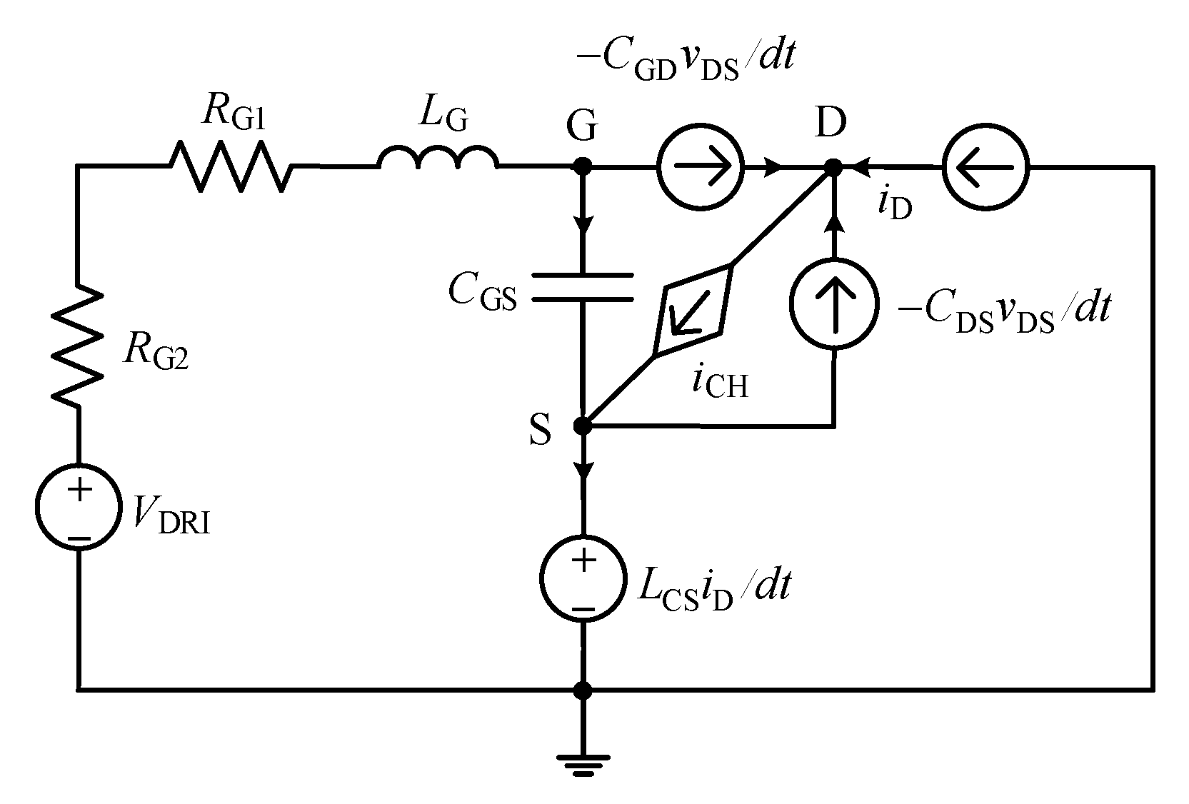
Since the gate of the non-Kelvin structure SiC MOSFET has a common source inductor LCS, when Q1 is turned on, the rapidly changing drain current will generate a common source voltage on the common source inductor. The common source voltage can be expressed by Equation (4):
v C S ( t ) = L C S × d i D ( t ) d t
Due to the existence of the common source inductor, when the rate of change of the drain current increases, a common source voltage with a larger amplitude will be generated on the common source inductor. Figure 3 shows the equivalent circuit diagram of this stage, considering the common source inductor LCS. According to Figure 3, the equivalent driving voltage at this stage can be expressed by Equation (5). Since the polarity of the common source voltage and the driving voltage VDRI are opposite, the driving ability of the gate voltage decreases.
V D R I ( equ ) < V D R I L C S × d i D ( t ) d t
Stage 2. Drain-current rising time. Because the SiC MOSFET has an ultra-fast turn-on speed, the voltage of the drive circuit can easily satisfy Equation (6). When the driving circuit voltage satisfies Equation (6), namely, the sum of vCS and vGS is higher than the driving voltage VDRI. The gate voltage reversely charges and the gate drive voltage decreases. The drain current at this stage can be expressed by Equation (7) when considering the common source voltage [2,22,25]. With the increase in the drain current turn-on speed, the drain current of Q1 will seriously oscillate in stage 2, and the switch will even turn off by mistake.
V D R I < v G S ( t ) + L C S × d i D ( t ) d t
i D ( t ) = g f × ( t 2 t 3 V D R I v G S ( t ) v C S ( t ) ( R G 1 + R G 2 ) C G S d t )
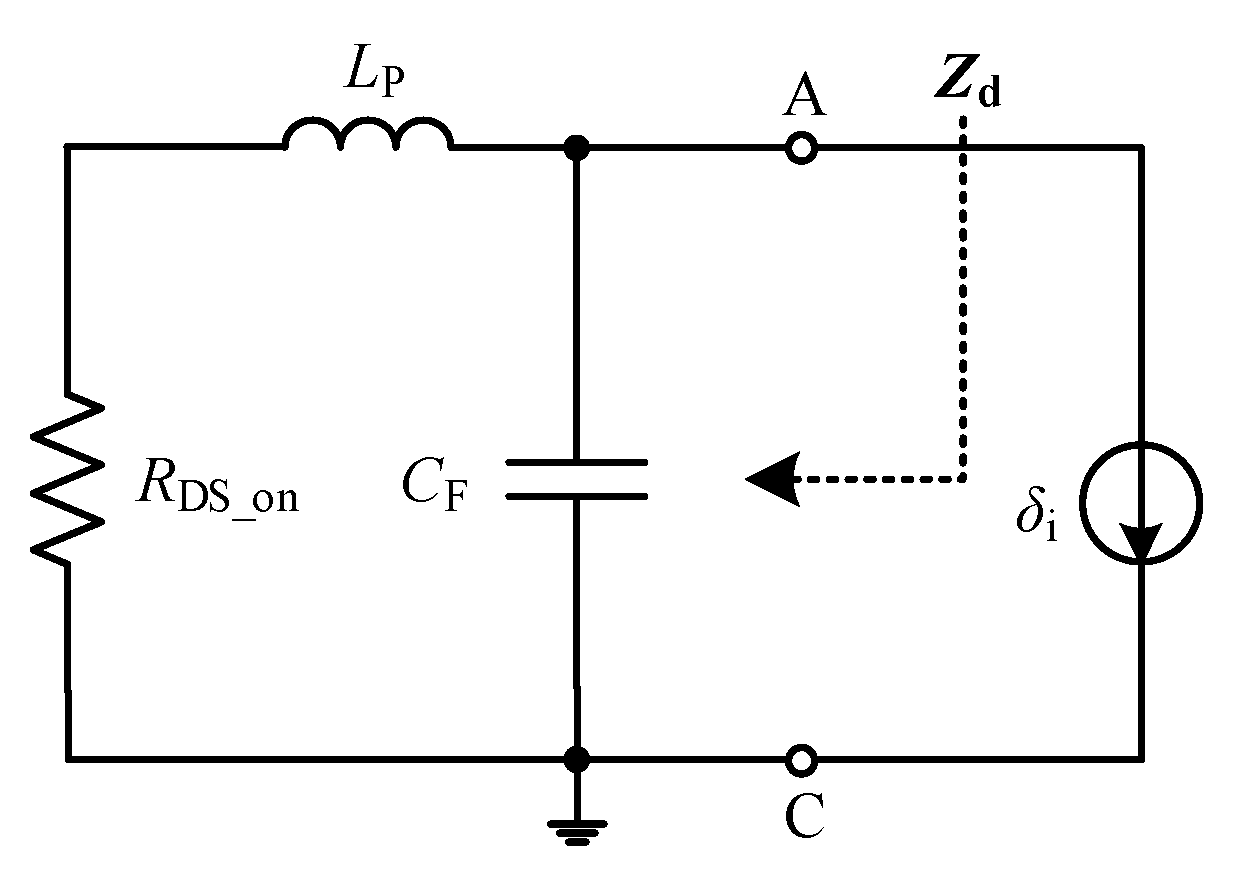
Stage 3. Drain-source voltage fall time. When considering the common source inductor, the operating state of stage 3 can be equivalent to the topology exhibited in Figure 4. The channel of the SiC MOSFET will be fully turned on at this stage, and the drain current will resonate under the influence of the diode junction capacitance CF and the parasitic inductor LP. The drain current resonance frequency is shown in Equation (8). The high-frequency resonant drain current causes the common source voltage to oscillate seriously, and the severely oscillated common source voltage may easily cause reverse charging of the drive circuit. The drain-source voltage at this stage can be expressed by Equation (9). According to the expression of the drain-source voltage at this stage, it can be known that the reverse charging of the driving circuit will suppress the drop of the drain-source voltage, and even cause Q1 to be turned off in error.
f 1 2 π L P C F
d v D S d t V D R I v C S ( t ) v G S ( t ) ( R G 1 + R G 2 ) C G D

3. SRD-Type Drive Circuit

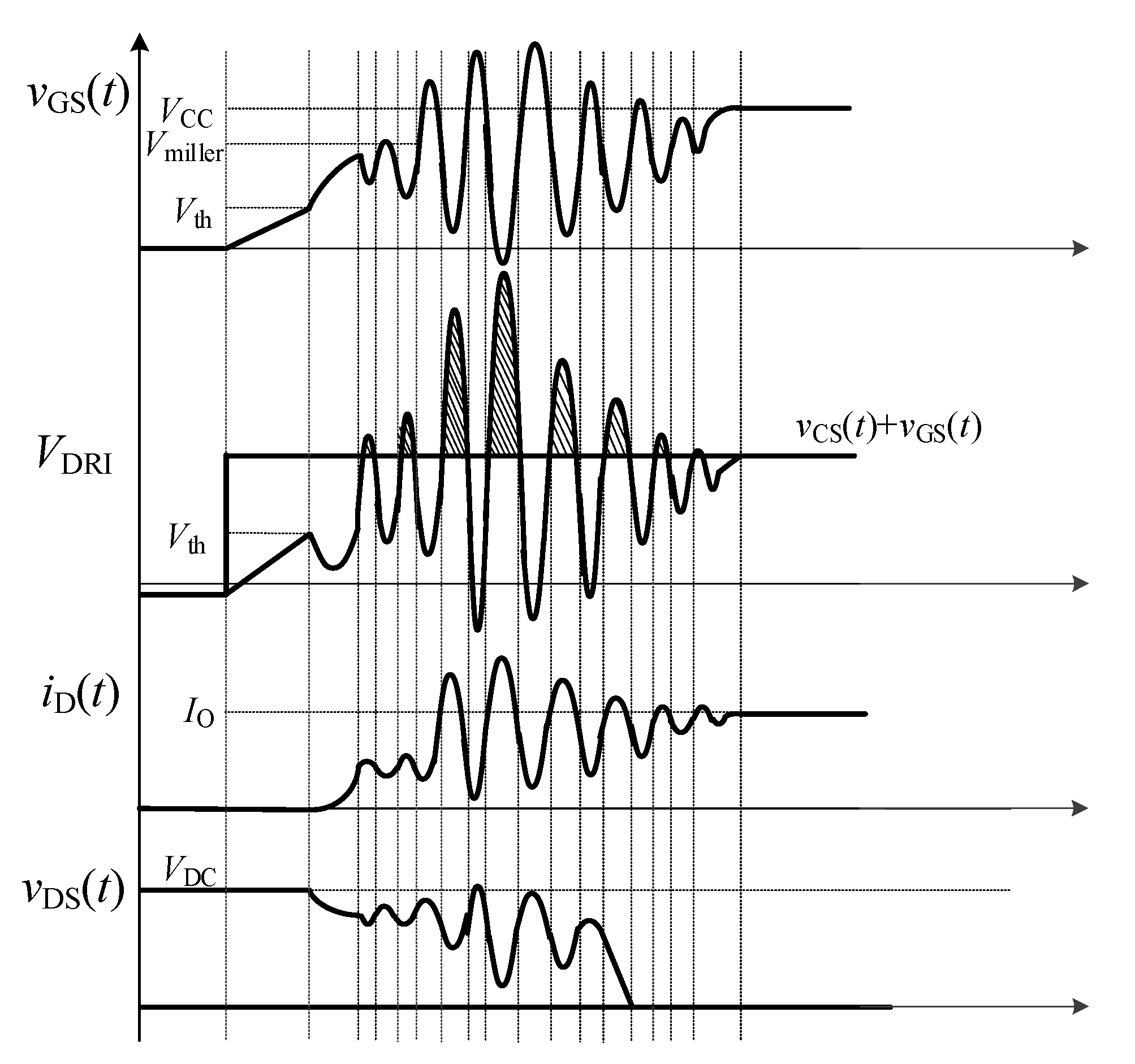
Based on the above analysis, the most effective way to reduce turn-on losses is to increase turn-on speed [21,22]. However, for a non-Kelvin packaged SiC MOSFET, as the turn-on speed increases, the common source voltage superimposed in the SiC MOSFET drive circuit is likely to cause the drive circuit to reverse-charge. The reverse-charging process of the driving circuit will cause the drain-source voltage oscillation of the SiC MOSFET [24]. The schematic waveforms of the vGS, iD and vDS of a non-Kelvin packaged SiC MOSFET with high turn-on speed are shown in Figure 5. When the voltage relationship of the driving circuit satisfies Equation (6), the driving circuit reversely charges, as shown in the pink area in Figure 5. The reverse charging of the drive circuit will not only reduce the turn-on speed of the SiC MOSFET, but also cause the gate-source voltage to oscillate and even cause the SiC MOSFET to turn off in error.
Therefore, this paper proposes an SRD-type drive circuit that suppresses the turn-on oscillation of a non-Kelvin packaged SiC MOSFET by blocking the reverse charging process of the common-source voltage on the gate of the switch, thereby reducing the turn-on loss.

3.1. Operating Principle of SRD-Type Drive Circuit

The structure of the SRD-type drive circuit is shown in Figure 6. Compared with the traditional driving circuit, the SRD-type drive circuit blocks the reverse charging loop by adding a low-voltage diode to the turn-on loop of the driving circuit, and the drive circuit structure is simple.
The working principle of the SRD-type drive circuit is as follows:
Stage 1. Turn-on delay time. Since the SiC MOSFET is in the off state at this stage, the SRD-type drive circuit works in the same way as the traditional driving circuit.
Stage 2. Drain-current rising time. The channel of Q1 starts to open when the value of vGS exceeds the threshold voltage, i.e., Vth. At the same time, the drain current rises rapidly. The rapidly rising drain current generates a common source voltage with a polarity opposite to the driving voltage VDRI on the common source inductor. According to Equation (5), the common source voltage at this stage will cause the equivalent driving voltage of the driven circuit to drop, and the common source voltage hinders the rate of change of the drain current. When the voltage relationship of the driving circuit satisfies Equation (6), the diode of the SRD-type drive circuit blocks the reverse-charging circuit of the driving circuit. When the polarity of the common source voltage changes as the drain current oscillates, the equivalent drive voltage of the drive circuit rises, and the common source voltage accelerates the rate of rise of the drain current.
Stage 3. Drain-source voltage fall time. At this stage, it can be known that the channel of the switch Q1 has been fully turned on and the channel opens completely, and the reverse current iF of D charges the diode parasitic capacitor CF. Because the gate-source voltage vGS has a large amplitude at this stage, the voltage relationship of the driving loop can easily satisfy the formula (6). When the voltage of the driving circuit satisfies the formula (6), the diode in the SRD-type drive circuit blocks the reverse charging circuit of the driving circuit to avoid the reduction in the vGS, thereby suppressing the drain-source voltage oscillation.
Stage 4. Turn-on oscillation stage. The gate-source voltage has risen to the driving voltage at this stage, and the amplitude oscillation of the common source voltage is small. Therefore, reverse charging does not easily occur in the drive circuit, and the working principle of the SRD-type drive circuit and the traditional drive circuit at this stage is consistent.

3.2. Simulation Verification

To test the feasibility and effectiveness of the presented SRD-type drive circuit, for this paper we built a double-pulse test circuit based on LTspice software, to compare the turn-on waveforms of the traditional drive circuit and the SRD-type drive circuit. The device under test is a 1200 V SiC MOSFET which is produced by CREE, and the device under test is C2M0080120D. The freewheeling diode uses a 1200 V SiC diode. Table 1 lists the specific parameters of the double-pulse simulation experimental test platform.
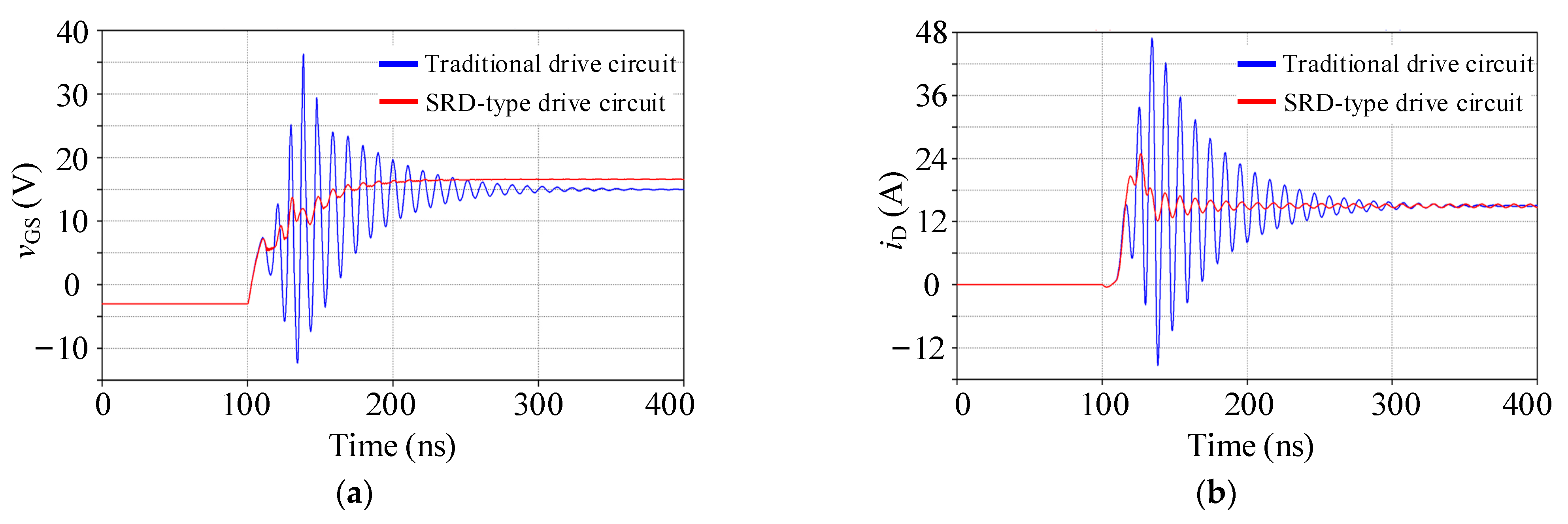
The turn-on process comparison waveforms under different drive circuits are shown in Figure 7. Table 2 gives the simulation comparison results of the opening process. The simulation comparison results show that the turn-on losses of the two driving circuits are basically equal under the same driving parameters. When using a traditional drive circuit, the gate-source voltage forward voltage spike is 36.5 V. In the actual circuit, a gate-source forward voltage spike with such a large amplitude will cause the gate-source forward breakdown of the SiC MOSFET. What is more, the negative oscillation of the gate-source voltage will cause the gate voltage to be lower than the threshold voltage during the turn-on process, when the traditional driving method is applied. Q1 is turned off by mistake many times. In addition, the turn-on oscillation phenomenon of Q1 is very serious.
When the SRD-type drive circuit is adopted in the test circuit, the gate-source voltage of Q1 has no obvious oscillation, and the maximum voltage spike of the gate voltage of Q1 is 16.8 V, which is within the safe range of the gate-source voltage. Since gate-source voltage oscillations of Q1 are effectively suppressed, drain current and drain-source voltage oscillations of Q1 are also effectively suppressed. When the SRD-type drive circuit is adopted, the drain-source voltage spike of Q1 is reduced by 186 V, and the drain current spike is reduced by 22 A. The drive circuit based on the proposed SRD-type drive circuit works stably at a high turn-on speed, and the turn-on loss of Q1 is significantly reduced.

4. Experimental Verification

For testing the practicability and effectiveness of an SRD-type drive circuit on the practical circuit occasions, a double-pulse experimental test platform with the same working conditions as the simulation platform is built. The experimental circuit uses the same device under test as the simulation circuit.
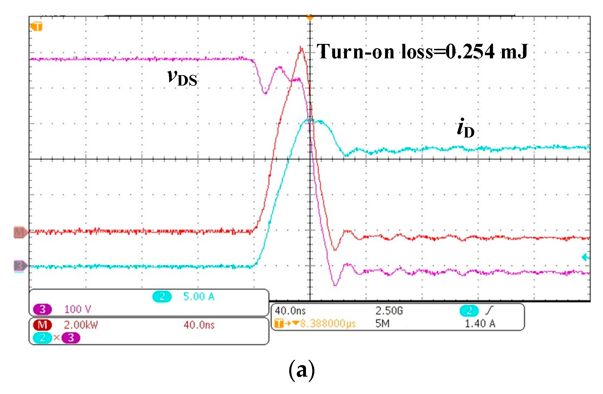
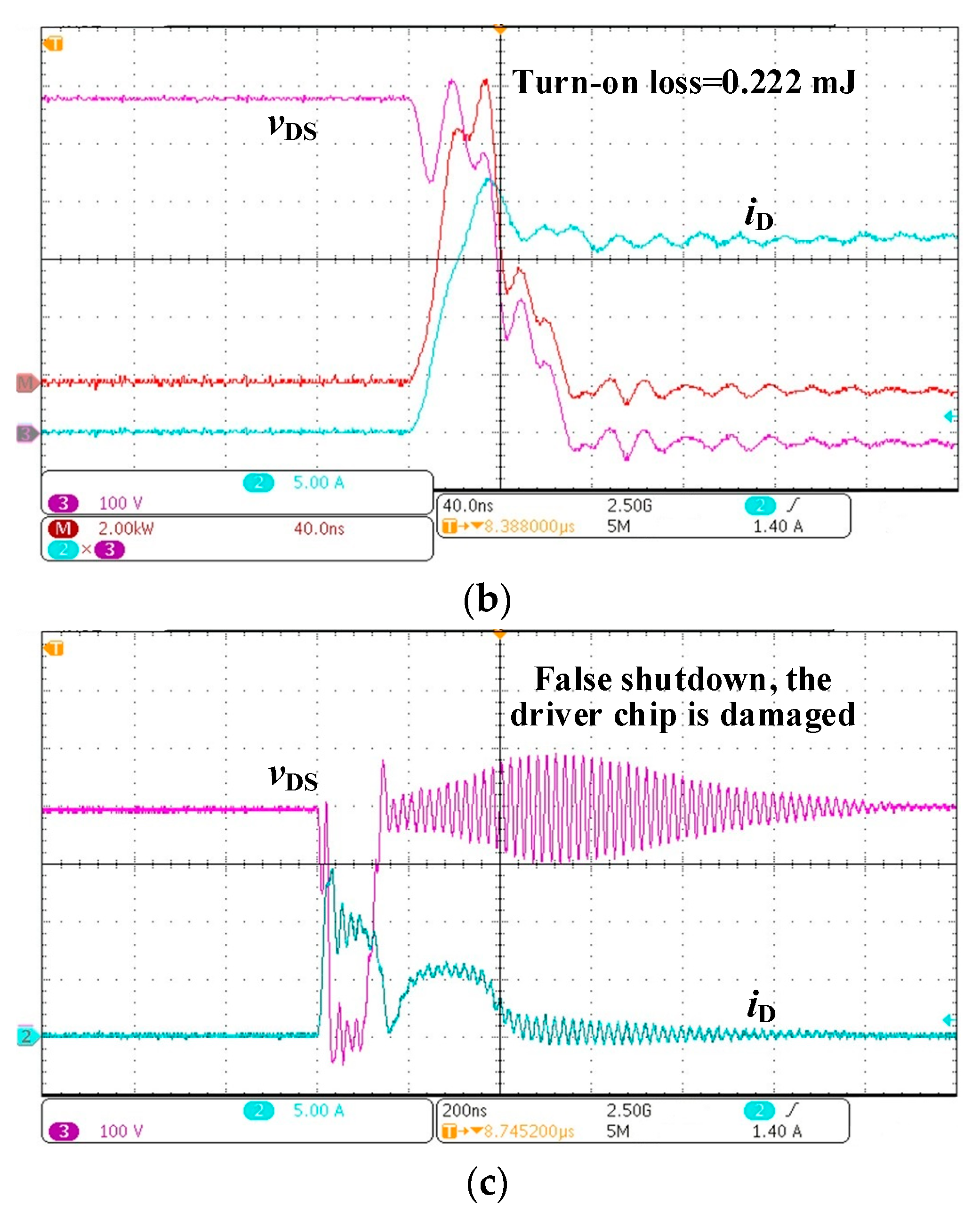
Figure 8 shows the waveforms of the turn-on process of the SiC MOSFET Q1 based on the traditional driving circuit. The turn-on waveforms indicate that the SiC MOSFET can work reliably with a 10 Ω gate resistor. When the gate resistor is reduced to 3 Ω, the drain current and the drain-source voltage of Q1 oscillate seriously during the turn-on process. As the external gate resistor is further reduced to 1.5 Ω, the device’s gate-source voltage, drain current, and drain-source voltage oscillations become more severe, and the gate-source voltage oscillation spikes cause damage to the driver chip.
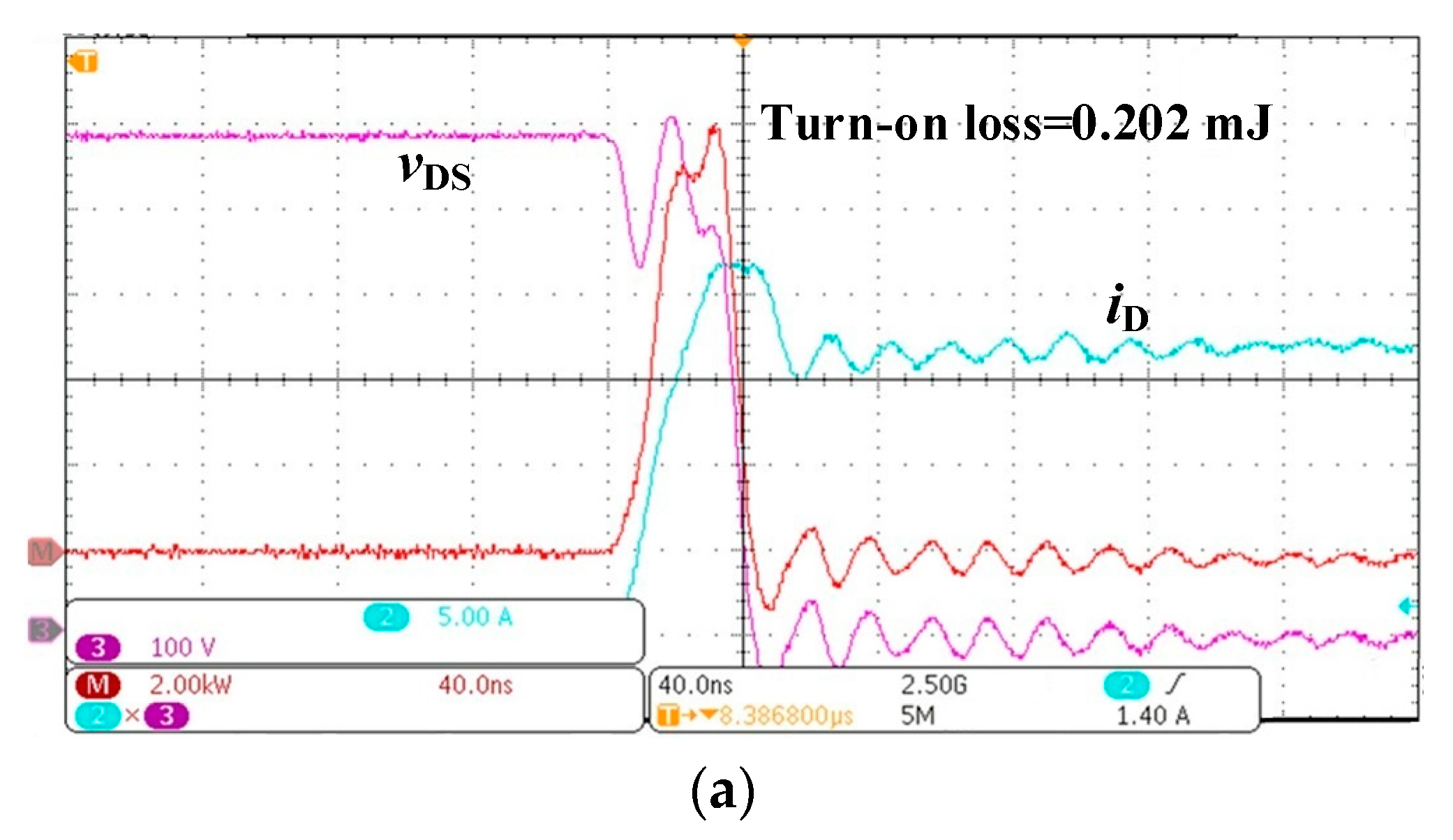
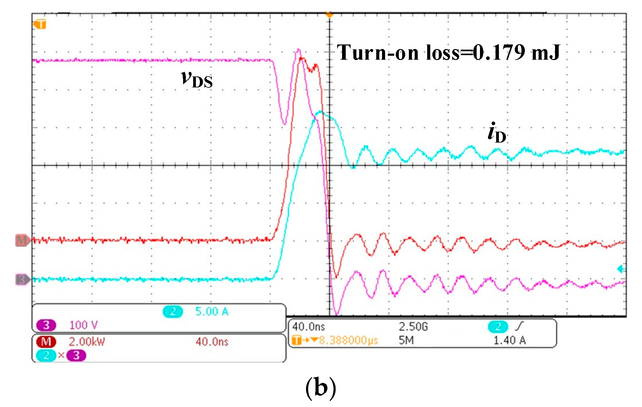
Figure 9 shows the turn-on waveform of the double-pulse circuit, based on the SRD-type drive circuit. The turn-on waveform indicates that SiC MOSFET can work reliably based on the SRD-type drive circuit with a 1.5 Ω external resistor. For the purpose of reducing the turn-on loss furtherly, a 0 Ω gate resistor is used in the SRD-type drive circuit during the turn-on process of the device. The experimental waveform is shown in Figure 9b. The experimental results show that when the 0 Ω gate resistor is applied to the SRD-type drive circuit, SiC MOSFET can be turned on normally. When the SRD-type drive circuit uses a 0 Ω gate resistor, the turn-on loss of the SiC MOSFET is reduced to 0.179 mJ. Compared with the use of a 10 Ω external resistor, the turn-on loss of the SiC MOSFET is reduced by one-third.

5. Conclusions

This paper first analyzes the effect of the common source inductor of the non-Kelvin packaged SiC MOSFET on the turn-on oscillation of the SiC MOSFET. Based on theoretical analysis, this paper proposes an SRD-type drive circuit that can suppress the effect of the common source inductor on the SiC MOSFET turn-on oscillation. The SRD-type drive circuit can ensure that the SiC MOSFET avoids the reverse charging process of the drive circuit at a high turn-on speed, thereby suppressing the turn-on oscillation of non-Kelvin packaged SiC MOSFET. Experimental comparison results show that the SRD-type drive circuit can effectively suppress the turn-on oscillation of non-Kelvin packaged SiC MOSFET, thereby reducing turn-on losses.

Author Contributions

Conceptualization, H.Z.; methodology, H.Z. and Y.L.; validation, J.C. and H.Z.; writing—original draft preparation, J.C.; writing—review and editing, H.Z.; project administration, Y.L.; Guidance and advice, F.L. All authors have read and agreed to the published version of the manuscript.

Funding

This research received no external funding.

Institutional Review Board Statement

Not applicable.

Informed Consent Statement

Not applicable.

Data Availability Statement

Data is available on request from the authors. The data that support the findings of this study are available from the corresponding author upon reasonable request.

Conflicts of Interest

The authors declare no conflict of interest.

References

  1. Wrzecionko, B.; Bortis, D.; Biela, J.; Kolar, J.W. Novel AC-coupled gate driver for ultrafast switching of normally off SiC JFETs. IEEE Trans. Power Electron. 2012, 27, 3452–3463. [Google Scholar] [CrossRef]
  2. Chen, J.G.; Li, Y.; Liang, M. A Gate Driver Based on Variable Voltage and Resistance for Suppressing Overcurrent and Overvoltage of SiC MOSFETs. Energies 2019, 12, 1640. [Google Scholar] [CrossRef] [Green Version]
  3. Han, D.; Noppakunkajorn, J.; Sarlioglu, B. Analysis of a SiC three-phase voltage source inverter under various current and power factor operations. In Proceedings of the IECON 2013-39th Annual Conference of the IEEE Industrial Electronics Society, Vienna, Austria, 10–13 November 2013; pp. 447–452. [Google Scholar]
  4. Jouha, W.; El Oualkadi, A.; Dherbecourt, P.; Joubert, E.; Masmoudi, M. Silicon Carbide Power MOSFET Model: An Accurate Parameter Extraction Method Based on the Levenberg–Marquardt Algorithm. IEEE Trans. Power Electron. 2018, 33, 9130–9133. [Google Scholar] [CrossRef]
  5. Han, D.; Noppakunkajorn, J.; Sarlioglu, B. Efficiency comparison of SiC and Si-based bidirectional DC-DC converters. In Proceedings of the 2013 IEEE Transportation Electrification Conference and Expo (ITEC), Detroit, MI, USA, 16–19 June 2013. [Google Scholar]
  6. Hashimoto, K.; Okuda, T.; Hikihara, T. A Flyback Converter with SiC Power MOSFET Operating at 10 MHz: Reducing Leakage Inductance for Improvement of Switching Behaviors. In Proceedings of the 2018 International Power Electronics Conference (IPEC-Niigata 2018 -ECCE Asia), Niigata, Japan, 20–24 May 2018; pp. 3757–3761. [Google Scholar]
  7. Zhang, W.; Xu, Z.; Zhang, Z.; Wang, F.; Tolbert, L.M.; Blalock, B.J. Evaluation of 600 V cascode GaN HEMT in device characterization and all-GaN-based LLC resonant converter. In Proceedings of the Energy Conversion Congress and Exposition, Denver, CO, USA, 15–19 September 2013; pp. 3571–3578. [Google Scholar]
  8. Zhang, W.; Zhang, Z.Y.; Wang, F.; Tolbert, L.M.; Costinett, D.; Blalock, B. Characterization and Modeling of a SiC MOSFET’s Turn-Off Overvoltage. Mater. Sci. Forum 2018, 924, 827–831. [Google Scholar] [CrossRef]
  9. Kadavelugu, A.; Baek, S.; Dutta, S.; Bhattacharya, S.; Das, M.; Agarwal, A.; Scofield, J. High-frequency design considerations of dual active bridge 1200 V SiC MOSFET DC-DC converter. In Proceedings of the 2011 Twenty-Sixth Annual IEEE Applied Power Electronics Conference and Exposition (APEC), Fort Worth, TX, USA, 6–11 March 2011; pp. 314–320. [Google Scholar]
  10. Wang, Y.; De Haan, S.W.H.; Ferreira, J.A. Potential of improving PWM converter power density with advanced components. In Proceedings of the 2009 13th European Conference on Power Electronics and Applications, Barcelona, Spain, 8–10 September 2009; pp. 1–10. [Google Scholar]
  11. Strydom, J.; De Rooij, M.; Van Wyk, J. A comparison of fundamental gate-driver topologies for high frequency applications. In Proceedings of the Nineteenth Annual IEEE Applied Power Electronics Conference and Exposition, APEC’04, Anaheim, CA, USA, 22–26 February 2004; Institute of Electrical and Electronics Engineers (IEEE): New York, NY, USA, 2004; Volume 2, pp. 1045–1052. [Google Scholar]
  12. Zhang, Z.; Wang, F.; Tolbert, L.M.; Blalock, B.J.; Costinett, D.J. Realization of high speed switching of SiC power devices in voltage source converters. In Proceedings of the 2015 IEEE 3rd Workshop on Wide Bandgap Power Devices and Applications (WiPDA); Institute of Electrical and Electronics Engineers (IEEE), Blacksburg, VA, USA, 2–4 November 2015; pp. 28–33. [Google Scholar]
  13. Zhang, Z.; Wang, F.; Tolbert, L.M.; Blalock, B.J. Active Gate Driver for Crosstalk Suppression of SiC Devices in a Phase-Leg Configuration. IEEE Trans. Power Electron. 2014, 29, 1986–1997. [Google Scholar] [CrossRef]
  14. Swamy, M.M.; Kume, T.; Takada, N. An efficient resonant gate-drive scheme for high-frequency applications. IEEE Trans. Ind. Appl. 2012, 48, 1418–1431. [Google Scholar] [CrossRef]
  15. Jorge, G.; Sara, S.; Emre, G.; Alberto, C. Self-Powering High Frequency Modulated SiC Power MOSFET Isolated Gate Driver. IEEE Trans. Ind. Appl. 2019, 55, 3967–3977. [Google Scholar]
  16. Gui, H.; Zhang, Z.; Chen, R.; Niu, J.; Tolbert, L.M.; Wang, F.F.; Costinett, D.; Blalock, B.J.; Choi, B.B. Gate Drive Technology Evaluation and Development to Maximize Switching Speed of SiC Discrete Devices and Power Modules in Hard Switching Applications. IEEE J. Emerg. Sel. Top. Power Electron. 2020, 8, 4160–4172. [Google Scholar] [CrossRef]
  17. Wang, X.; Zhao, Z.; Li, K.; Zhu, Y.; Chen, K. Analytical Methodology for Loss Calculation of SiC MOSFETs. IEEE J. Emerg. Sel. Top. Power Electron. 2019, 7, 71–83. [Google Scholar] [CrossRef]
  18. Li, C.; Lu, Z.; Chen, Y.; Li, C.; Luo, H.; Li, W.; He, X. High Off-State Impedance Gate Driver of SiC MOSFETs for Crosstalk Voltage Elimination Considering Common-Source Inductance. IEEE Trans. Power Electron. 2020, 35, 2999–3011. [Google Scholar] [CrossRef]
  19. Zhao, J.; Wu, L.; Li, Z.; Chen, Z.; Chen, G. Analysis and Suppression for Crosstalk in SiC MOSFET Turn-off Transient. In Proceedings of the 2020 IEEE 9th International Power Electronics and Motion Control Conference, Nanjing, China, 29 November–2 December 2020; pp. 1145–1150. [Google Scholar]
  20. Sakib, N.; Manjrekar, M.; Ebong, A. An overview of advances in high reliability gate driving mechanisms for SiC MOSFETs. In Proceedings of the 2017 IEEE 5th Workshop on Wide Bandgap Power Devices and Applications (WiPDA), Albuquerque, NM, USA, 30 October–1 November 2017; pp. 291–294. [Google Scholar]
  21. Gui, H.; Sun, J.; Tolbert, L.M. Charge Pump Gate Drive to Reduce Turn-ON Switching Loss of SiC MOSFETs. IEEE Trans. Power Electron. 2020, 35, 13136–13147. [Google Scholar] [CrossRef]
  22. Xiao, L.; Zhao, J.; Li, P.; Dongdong, C.; Wu, L. Analysis and Suppression of High Speed Dv/Dt Induced False Turn-on in GaN HEMT Phase-Leg Topology. Access IEEE 2021, 9, 45259–45269. [Google Scholar]
  23. Zhou, Z.; Li, H.; Wu, X. A Constant Frequency ZVS Control System for the Four-Switch Buck–Boost DC–DC Converter With Reduced Inductor Current. IEEE Trans. Power Electron. 2018, 34, 5996–6003. [Google Scholar] [CrossRef]
  24. Choudhury, A. Present Status of SiC based Power Converters and Gate Drivers—A Review. In Proceedings of the International Power Electronics Conference (IPEC-Niigata 2018-ECCE Asia), Niigata, Japan, 20–24 May 2018; pp. 3401–3405. [Google Scholar]
  25. Li, Y.; Liang, M.; Chen, J.G.; Zheng, T.Q.; Guo, H.B. A Low Gate Turn-OFF Impedance Driver for Suppressing Crosstalk of SiC MOSFET Based on Different Discrete Packages. IEEE J. Emerg. Sel. Top. Power Electron. 2019, 7, 353–365. [Google Scholar] [CrossRef]
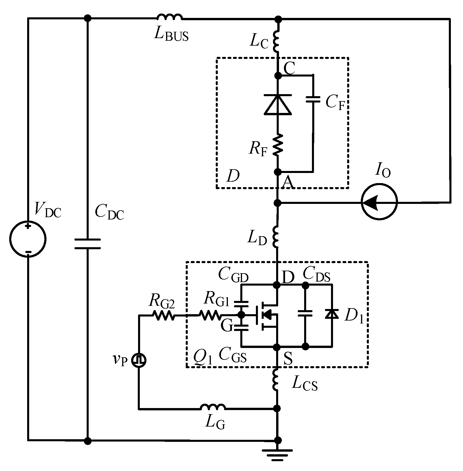
Figure 1. The double-pulse circuit when the parasitic parameters are studied.
Energies 14 02449 g001
Figure 2. Working process of one switching period of Q1 and D.
Energies 14 02449 g002
Figure 3. Equivalent circuit of stage 2.
Energies 14 02449 g003
Figure 4. Equivalent circuit of stage 3.
Energies 14 02449 g004
Figure 5. Turn-on waveforms based on a traditional driving circuit.
Energies 14 02449 g005
Figure 6. Schematic diagram of an SRD-type drive circuit.
Energies 14 02449 g006
Figure 7. The turn-on waveforms based on different drive circuits: (a) waveforms of gate-source voltage vGS, (b) waveforms of drain-current iD, (c) waveforms of drain-source voltage vDS, and (d) waveforms of turn-on loss p.
Energies 14 02449 g007aEnergies 14 02449 g007b
Figure 8. Turn-on waveform based on traditional drive circuit: (a) Ron = 10 Ω, (b) Ron = 3 Ω, and (c) Ron = 1.5 Ω.
Energies 14 02449 g008aEnergies 14 02449 g008b
Figure 9. Turn-on waveform based on an SRD-type drive circuit: (a) Ron = 1.5 Ω, and (b) Ron = 0 Ω.
Energies 14 02449 g009aEnergies 14 02449 g009b
Table 1. Specific parameters of the double-pulse simulation test platform.
Test Conditions
Input voltage VDC600 V
Output current IO15 A
Gate resistance Ron/Roff3 Ω
Table 2. Experimental comparison results of the turn-on process.
Contents of Comparison Traditional Driving CircuitSRD-Type Drive Circuit
Turn-on loss0.20 mJ0.21 mJ
Gate-source voltage spike36.5 V16.8 V
Drain current spike47 A25 A
Drain-source voltage spike768 V600 V
Publisher’s Note: MDPI stays neutral with regard to jurisdictional claims in published maps and institutional affiliations.