1. Introduction
With the rapid depletion of fossil fuels and the increasing pollution of the environment, it is urgent to develop clean and sustainable energy sources. In this context, the clean and abundant solar energy is one of the most ideal choices [
1]. Solar cells are advanced energy-conversion devices that effectively convert light energy into electrical energy directly through photoelectric or photochemical effects. Since the appearance of the first silicon-based solar cell in the 1950s, the development of solar cells has experienced following three stages. The first stage is silicon-based solar cells represented by monocrystalline silicon; the second stage is the thin-film solar cells represented by copper indium gallium selenide (known as CIGS); and the third stage is new types of solar cells based on novel materials and nanotechnologies, including dye-sensitized solar cells (DSSC) [
2], organic photovoltaics (OPV) [
3], quantum dot solar cells (QDSCs) [
4], etc. They have the advantages of simple manufacturing processes, low production costs, and high theoretical energy conversion efficiency. However, due to the poor environmental stability, they remain at the basic research stage in laboratories. In recent years, a new kind of solar cell called perovskite solar cell (PSC) has become a research hotspot in the photovoltaic field. In 2009, on the basis of dye-sensitized solar cells, Miyasaka et al. [
5] replaced the organic dyes with MAPbI
3 perovskite as the light absorption layer, realizing a photoelectric conversion efficiency of 3.8%, which opened the prelude of the study of PSCs. In the past 10 years, the photoelectric conversion efficiency of PSCs dramatically increased up to 25.2%, almost reaching the same level of crystalline silicon-based cells.
At present, there are four kinds of strategies to improve the photoelectric conversion efficiency of PSCs. The first kind of strategy is to prepare high-quality perovskite thin films. Burschka et al. [
6] adopted a typical two-step continuous deposition method to achieve the controllable morphology of perovskite films. Huang et al. [
7] invented the “gas-assisted liquid deposition (VASP)” method to improve the film quality. The second kind of strategy is to develop the new-typed electron transport layer (ETL) and hole transport layer (HTL). Hou et al. [
8] designed an α-Fe
2O
3/PCBM composite electron transport layer to improve the electron mobility. Ma et al. [
9] used the N-type semiconductor materials of ZnO to replace the conventional TiO
2, which facilitated the stimulation of electron–hole pairs, significantly improving the conductivity of the electron transport layer. Tom et al. [
10] improved the photoelectric conversion efficiency by optimizing the drying process of the hole transport layer of Spiro-OMeTAD in order to increase its stability. Que et al. [
11] used the NiO nanofilm as the hole transport layer of PSCs, thus leading to a satisfactory photoelectric conversion efficiency of 16.47%. The third kind of strategy is to optimize the interface to reduce the carrier loss at the interface, and thereby improve the photoelectric conversion efficiency of the battery. Snaith et al. [
12] modified the interface between the perovskite layer and the TiO
2 layer with C60-SAM, which effectively reduced the defect state at the interface and the probability of electron recombination. Zheng et al. [
13] introduced a type of quantum dot material between the absorption layer and the hole transport layer to regulate the energy band structure, increasing the short circuit current of PSCs. The fourth kind of strategy is to construct the novel battery structure. The structures of PSCs can be roughly divided into two types. One is mesoporous PSCs, which generally adopt TiO
2 mesoporous layer as the electron transport framework. Kim et al. [
14] achieved a photoelectric conversion efficiency of 9.7% by using mesoporous TiO
2 as the electron transport layer. The other is the planar heterojunction PSCs. Under the condition of light, the Wannier–Mott type excitons in the perovskite light absorbing layer can separate to generate electrons and holes, which move towards the poles driven by the internal potential, forming the “sandwich” structure [
15,
16]. Chen et al. [
17] changed the structure of traditional planar heterostructure PSCs into an inverted structure, which achieved an increased energy conversion efficiency of 15%. Compared with the mesoporous PSCs, the planar heterojunction PSCs exhibit the higher open circuit voltage and short circuit current, yet a worse hysteresis effect [
18].
The concept of photonic crystal (PC), which refers to a kind of artificial crystal structure formed by two or more materials with different dielectric constant arranged periodically in space, was first proposed by E. Yablonovitch and S. John in 1987 [
19,
20]. The main characteristic of such photonic crystal structure is the existence of a photonic band gap (PBG) in one or more directions. The interaction between the incident light and the PC material can be strengthened because the incident light in the forbidden band cannot transmit inside the photonic crystal.
Gomard’s team introduced a two-dimensional planar photonic crystal (2D PPC) structure into the absorption layer for a silicon-based solar cell, which improved the absorption efficiency of incident light [
21]. Dotermusch et al. [
22] introduced a hemispherical photonic crystal structure into the absorption layer of CuInSe (CIS) nanocrystalline-based solar cells, which greatly improved the light absorption capacity of the cells. Dong et al. [
23] introduced a two-dimensional nano disk array photonic crystal structure into the electron transport layer (ETL) of PSCs, which showed a strong optical reflection effect on the incident light, leading to the improved light collection efficiency of the absorption layer, and thus the increased photoelectric conversion efficiency of 19%. In addition, the introduction of photonic crystal structure can also change the band structure of the electron transport layer, making it much more conducive to the charge transport. Liu et al. [
24] designed a two-dimensional photonic crystal electron transport layer with inverse opal structured SnO
2-TiO
2, whose conduction band edge is more conducive to the transmission of electrons, therefore leading to the ideal photocurrent.
It can be seen that photonic crystals have been widely used as the electron transport layer or hole transport layer in solar cells. However, there are rare studies on the direct application of photonic crystals in the absorption layer, and the research on the optimization of the structure parameters of photonic crystals is not comprehensive. By rationally designing the structure of the absorption layer, the absorption efficiency of the absorption layer can be markedly improved, attributed to the “slow light” and band gap effect of the photonic crystal structure. Herein, a new absorption layer with photonic crystal structure is designed, and the optimal photonic crystal structure of the absorption layer is determined by optimizing the scatterer height H, scatterer diameter R, and lattice constant L of the photonic crystal structure.
2. Structural Design
Figure 1a schematically shows the overall structure of the PSC, which consists of Ag metal electrode, Spiro-OMeTAD hole transport layer, perovskite absorption layer with two-dimensional photonic crystal structure, dense TiO
2 electron transport layer, and FTO conductive glass.
Figure 1b shows the absorption layer with photonic crystal structure and the specific structure of single scattering element, where
H is the height of the scatterer,
R is the diameter of the scatterer, and
L is the lattice constant.
In this study, the widely used Methylamine lead iodide perovskite (CH
3NH
3PbI
3, MAPbI
3) was selected as the absorption layer material; it not only has a high extinction coefficient, a long carrier diffusion distance [
25,
26,
27,
28], and a low production cost, but also possess the characteristics of photo-generated carrier bipolar transmission [
29]. The scattering element medium of photonic crystal is cylindrical indium arsenide (InAs), which is arranged in the perovskite absorption layer according to the tetragonal lattice.
Figure 2 shows the absorption efficiency of several common semiconductor materials in the wavelength range of 400–1200 nm by the simulation. It can be found that the InAs has a high optical absorption efficiency, a band gap of only 0.45 eV, and an electron mobility of 3300 cm/V s [
30], indicating that it is a suitable semiconductor material with excellent photoelectric properties. In addition, the dense TiO
2 film and Spiro-OMeTAD are selected as the electron transport layer and hole transport layer, respectively [
14].
3. Results
It is well known that the wavelength distribution range of sunlight is 0–4000 nm. According to AM1.5G standard solar spectral data [
31], the solar radiation energy map is depicted in
Figure 3. It can be found that the solar radiation intensity is strongest in the wavelength range of 400–800 nm, which is roughly the range of visible light [
32]. In the near-infrared range, the solar radiation energy accounts for 54.3% of the total radiation energy in the wavelength range of 400–800 nm, while in the range of 800–1200 nm, the light radiation energy only accounts for 24.7%. Therefore, in the process of light absorption, the wavelength absorption in the range of 400–800 nm should be prioritized, and the wavelength absorption in the near-infrared range should be the auxiliary.
In our proposed work, the DiffractMOD module in Rsoft software designed by Synopsys is adopted to simulate the absorption of incident light in the wavelength range of 400–1200 nm using the InAs or air as cylindrical scatterers, respectively. The DiffractMOD module calculates the light absorption of photonic crystal structure absorption layer based on the rigorous coupled wave analysis (RCWA) [
21].
Figure 4a shows the variation of refractive index of MAPbI
3 with wavelength, while
Figure 4b shows the change of refractive index of InAs with wavelength. The refractive index data comes from the website “RefractiveIndex.INFO—Refractive index database”.
In this paper, we use the DiffractMOD module to design a two-dimensional perovskite photonic crystal absorption layer, as shown in
Figure 5.
Figure 5a is the stereoscopic view of the absorption layer, while
Figure 5b is the top view of the absorption layer structure. In the stereoscopic view, the red and green cylinders are the scatterers of the photonic crystal structure, and the yellow thin layer area at the bottom is the irradiation range of the incident light, corresponding to the purple frame of the top view. The blank area is filled with MAPbI
3 perovskite, as shown in
Figure 5b.
3.1. Arrangement of Cylindrical InAs Columns in MAPbI3 Perovskite Absorption Layer
When the InAs dielectric cylinder is selected as the scattering element, the scatterer height
H, scatterer diameter
R, and the lattice constant
L are optimized, and the corresponding simulation results are shown in
Figure 6.
Firstly, the influence of the variable
H on the absorption efficiency of the absorption layer was studied. Therefore,
R and
L were randomly taken as values of 0.3 μm and 0.5 μm, respectively. The simulated image is shown in
Figure 6a.
Figure 6a shows the absorptivity of InAs-filled tetragonal cylinder hole scatterers with different
H in MAPbI
3. The absorption efficiency increases with the increasing scatterer height
H. However, the thicker the layer is, the longer the migration distance of photogenerated carriers becomes in the absorption layer, leading to the increment of carrier recombination probability and the decrease in external quantum efficiency (EQE), which is not conducive to the improvement of photoelectric conversion efficiency. In order to analyze the relationship between the height of scatterer
H and the absorption efficiency in details, the absorption of incident light in the wavelength range of 400–800 nm by the absorption layer with different
H was calculated through the integration of
Figure 6a, as shown in
Table 1. When
H > 0.6 μm, the increase in absorption efficiency tends to be stable. Taking all facts into consideration, the best value of the scatterer height as
H = 0.6 μm is chosen.
Next, the influence of the variable
R on the absorption efficiency of the absorption layer was studied. Through the previous simulation, the optimal value of the scatterer height
H is determined to be 0.6 μm. Therefore, the scatterer height
H is taken as 0.6 μm, and the lattice constant
L is randomly taken as 0.4 μm. The simulated image is shown in
Figure 6b.
Figure 6b shows the absorptivity of InAs-filled tetragonal cylinder hole scatterers with different
R in MAPbI
3. When the scatterer diameter
R > 0.24 μm, the absorption efficiency of the absorption layer in the wavelength range of 400–700 nm begins to decrease. It is worth noting that such a decrease starts to decelerate at the wavelength of 500 nm where the sunlight has strong radiation energy. By summation, the absorption efficiency of the incident light in the wavelength range of 400–800 nm is shown in
Table 2. When the scatterer diameter
R increases, the absorption efficiency first increases followed by decreasing. The maximum absorption efficiency of 95.5% is reached when
R = 0.24 μm. Therefore,
R = 0.24 μm is chosen as the best value of the scatterer diameter.
Finally, the influence of the variable
L on the absorption efficiency of the absorption layer was studied. The best values of the scatterer height
H and scatterer diameter
R are taken respectively. The simulated image is shown in
Figure 6c.
Figure 6c shows the absorptivity of InAs-filled tetragonal cylinder hole scatterers with different
L in MAPbI
3. With the increase in the lattice constant
L, the absorption efficiency of the absorption layer for incident light in the wavelength range of 400–700 nm changes from dark red to red. Compared with the color code, the absorption efficiency is gradually increasing. The specific absorption values are shown in
Table 3. It can be seen that the absorption efficiency first increases followed by decreasing in the wavelength range of 400–800 nm. The maximum absorption efficiency can be reached when the lattice constant
L = 0.4 μm. Therefore,
L = 0.4 μm is selected as the optimal value of the lattice constant.
When the height of scatterer H, diameter of scatterer R, and lattice constant L are optimized, the absorption layer shows the absorption efficiency of 95.5% in the wavelength range of 400–800 nm, and 82.5% in the wide wavelength range of 400–1200 nm.
3.2. Arrangement of Cylindrical Air Holes in the MAPbI3 Perovskite Absorption Layer
When the air is selected as the scattering element, the three parameters
H,
R, and
L are also optimized, and the corresponding simulation results are shown in
Figure 7.
Similarly, the influence of the variable
H on the absorption efficiency of the absorption layer was firstly studied.
R and
L were randomly taken as 0.2 μm and 1.6 μm. The simulated image is shown in
Figure 7a.
Figure 7a shows the absorptivity of air-filled tetragonal cylinder hole scatterers with different
H in MAPbI
3. The absorption efficiency increases with the increase in the scatterer height
H. The absorption efficiency at different scatterer heights
H is summarized in
Table 4. In order to make a comparison with the absorption efficiency data in the previous section, the optimal value of
H at this time is also selected as 0.6 μm. It can be seen that the absorption efficiency of the absorption layer is 91.1% in the wavelength range of 400–800 nm at
H = 0.6 μm.
Then the influence of the variable
R on the absorption efficiency of the absorption layer was studied. The optimal scatterer height was 0.6 μm, which was determined in the previous simulation. The lattice constant
L is randomly taken as 1.1 μm. The simulated image is shown in
Figure 7b.
Figure 7b shows the absorptivity of air-filled tetragonal cylinder hole scatterers with different
R in MAPbI
3. The absorption efficiency decreases with the increase in the scatterer diameter
R. The absorption efficiency at different scatterer diameters is summarized in
Table 5. When
R = 0.1 μm, the absorption efficiency of the absorption layer reaches the maximum of 90.9% at 400–800 nm. Therefore,
R = 0.1 μm is chosen as the optimal value of the scatterer diameter.
Finally, the influence of the lattice constant
L on the absorption efficiency of the absorption layer was studied. The scatterer height
H and the scatterer diameter
R were taken as the optimal values, respectively. The simulate image is shown in
Figure 7c.
Figure 7c shows the absorptivity of air-filled tetragonal cylinder hole scatterers with different
L in MAPbI
3. With the increase in the lattice constant
L, the absorption efficiency first increases, and then remains almost unchanged, which is also confirmed by
Table 6. When the lattice constant
L > 1.4 μm, the increase in the absorption efficiency becomes negligible. Therefore,
L = 1.4 μm is the best value of the lattice constant, at which the absorption efficiency of incident light in the wavelength range of 400–800 nm is 91.0%.
When the height of scatterer H, diameter of scatterer R, and lattice constant L are optimized, the absorption layer shows the absorption efficiency of 91.1% in the wavelength range of 400–800 nm, and 51.3% in the wide wavelength range of 400–1200 nm.
4. Discussion
In order to compare with the absorption layer with photonic crystal structure, the absorption efficiency of the pure MAPbI
3 perovskite absorption layer with the same thickness was measured.
Figure 8 shows the absorption efficiencies of different absorption layers measured in the wavelength range of 400–1200 nm by the simulation. It can be seen that compared with the pure MAPbI
3 perovskite absorption layer, the absorption layer with photonic crystal structure has the higher absorption efficiency for incident light. In addition, the absorption efficiency of the 2D photonic crystal with InAs is higher than that of air.
It should be noted here that the absorption efficiency of the InAs cylindrical scatterer absorption layer presented in
Figure 8 is based on a perfect photonic crystal structure. In fact, this is an ideal state. Crystal defects, such as point defects, line defects, and so on, are inevitable in the process of photonic crystal fabrication, causing some errors in the absorption efficiency of the absorption layer. In order to make the data more scientific and precise, the absorption efficiency of the photonic crystal absorption layer with two kinds of crystal defects is simulated in this paper, and the corresponding error bars are proposed.
Figure 9 is a schematic diagram of the photonic crystal structure absorption layer with two kinds of crystal defects.
Figure 9a shows the absorption layer of photonic crystal structure with point defects, while
Figure 9b shows the absorption layer of photonic crystal structure with line defects.
The absorption efficiency of the absorption layer with two kinds of defect structures obtained by simulation is shown in
Figure 10. According to
Figure 10, the error caused by the defect structure for the absorption efficiency of short-wavelength incident light was small, while the error for the absorption efficiency of long-wavelength incident light was large.
Next, to clarify the enhancement effect of pure InAs PC on the absorption efficiency in the absorption layer, the absorption efficiency of InAs PC filled with air with the same design was further simulated, as shown in
Figure 11. The absorption efficiency of pure InAs PC is 73.0%, while the absorption efficiency of pure MAPbI
3 perovskite is 48.5%. The total absorption efficiency in the composite system of InAs PC + MAPbI
3 is 82.5%, which fully shows that the InAs PC makes the absorption efficiency of MAPbI
3 perovskite solar cells experience a huge improvement.
In fact, the improvement of absorption efficiency can be attributed to the “slow light” effect and band gap effect of photonic crystal structure [
32]. When the incident light propagates in the photonic crystal, the inhomogeneous medium induces a very strong scattering to the light, which forms a coupling effect with the Bragg scattering in the crystal and creates the photonic band gap. This gap can prevent the incident light whose frequency falls within the photonic band gap from transmitting in the crystal, therefore achieving a high reflection efficiency of this part of light, enhancing the interaction between the light and the matter, and increasing the light absorption efficiency. As is well known, the “slow light” effect can be formed by strong dispersion. The photonic crystal is a specific structure with periodic refractive index change, which can produce a strong dispersion effect. According to the microscopic mechanism of dielectric polarization, there is a large change of the refractive index at the resonance frequency of the medium, which can effectively slow down the propagation speed of light. At the same time, there is a strong absorption at the resonance frequency of the medium, which makes it difficult for light waves to be absorbed through the medium. In this way, the photonic crystal structure is helpful for the improvement of light absorption.
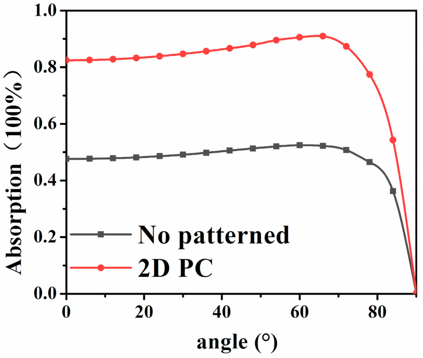
In addition, the dependency of the absorbing layer on the angle of incident light is analyzed when the height of the scatterer
H, the diameter of the scatterer
R, and the lattice constant
L are optimized. When the incident light angle changes, the cosine loss will inevitably occur on the surface of the battery [
33], resulting in the reduction of photoelectric conversion efficiency. Through the introduction of photonic crystal structure and the use of its “slow light” and band gap effect, the interaction between incident light and absorptive layer material is increased, leading to the improved absorption efficiency, and thus the compensated cosine loss caused by the angle change of incident light. In this study, the effect of light incident angle on the absorption efficiency of the absorption layer was simulated in the range of 0–90°. As shown in
Figure 12, compared with the absorption layer without photonic crystal structure, the absorption efficiency of the absorption layer containing photonic crystal structure is about 80% in the incident light angle range of 0–80°, which proves that the absorption layer with photonic crystal structure is robust to the incident light angle.
Meanwhile, in order to investigate the influence of the lattice arrangement and the scatterer shape on the absorption efficiency of the optical absorption layer, the case of hexagonal lattice arrangement and ellipsoidal scatterer was also discussed. The simulation results of the absorption efficiency are shown in
Figure 13. As shown in
Figure 13a, the absorption efficiency of the optical absorption layer where the scatterers are arranged in a hexagonal lattice is weaker than that of a tetragonal lattice in the wavelength range of 700–1200 nm.
Figure 13b shows the change of absorption efficiency with different wavelength when the scatterers are ellipsoidal. When the scatterers are elliptic cylinders, the absorption efficiency is lower than that of the cylindrical scatterers, no matter in tetragonal or hexagonal lattices. It is more comprehensive and objective to conclude that the optimal structure of the absorption layer is the cylindrical scatterer arranged in a tetragonal lattice.
5. Conclusions
In summary, the perovskite material has excellent photoelectric properties, possessing the ability to subvert the existing photovoltaic pattern. Previously, researchers mainly focused on the energy conversion efficiency and the stability of perovskite solar cells. As for the application of photonic crystal structure in perovskite solar cells, most researchers designed it as a Bragg reflector, which made the incident light passing through the absorption layer for the first time reflect back to the absorption layer again and increased the interaction between the incident light and the absorption layer material, so as to improve the light absorption efficiency. However, the shortcoming of this design is that the light reflected back to the absorption layer may pass through the absorption layer again, leading to the secondary loss of incident light and insignificant improvement of light absorption efficiency. In this study, from the perspective of how to improve the absorption efficiency of the perovskite absorption layer, the photonic crystal structure is designed directly in the absorption layer to avoid the secondary loss of incident light. The photonic band gap and “slow light” effect of the photonic crystal structure are used to bind the incident light in the absorption layer as much as possible, so that the interaction between the incident light and the absorption layer material is strengthened. In this way, the light absorption efficiency can be greatly improved. The best absorption layer structure is determined by optimizing the parameters of the scatterer. The highest absorption efficiency of 82.5% is obtained when the InAs cylindrical scatterers with the scatterer height H of 0.6 μm, the scatterer diameter R of 0.24 μm, and the lattice constant L of 0.4 μm are arranged in a tetragonal lattice. Compared with the pure MAPbI3 perovskite absorption layer, the absorption efficiency of the novel absorption layer is increased by 70.1%. In addition, this kind of two-dimensional nano column or hole photonic crystal structure has high controllability, and the photogenerated carriers can transport along the column or hole wall. This reduces the exciton recombination at the interface between grains, leading to the increase in the photocurrent inside the cell. Moreover, the designed photonic crystal structure is facile for preparation. The electron beam etching techniques can fabricate micro-nano structures with an accuracy of less than 5 nm at present. Hence, the photonic crystal structures can be prepared by electron beam etching techniques and vapor deposition technology. Therefore, this work provides a new research direction for the structural design of absorption layers for high-performance PSCs in the near future.


