1. Introduction
Thermal management currently represents a very important design issue, if the safe and stable operation of any electronic system is required. Focusing on the applications of power electronic systems, the mentioned phenomena is defined as one of the figures of merit for the evaluation of the operational characteristics. This is also due to the continuous increase in the power density of power electronic system and devices [
1,
2,
3,
4]. If semiconductor components are analyzed in more detail, it will be discovered that packing technology is improving from year to year, thus optimizing the operational performance of semiconductor devices. Currently, many types of packages are at the disposal from semiconductor manufacturers, while they represent a key ability in defining thermal properties. Thermal management is key design aspect if reliability and operational life of individual electronic components are considered. Therefore, it is recommended at the preliminary construction stage of the system that a precise analysis of the thermal performance is provided [
5,
6,
7,
8,
9].
The ways showing how to optimize thermal management of electronic components, and thus performance of electronic systems, have been mostly based on experimental measurements. However, nowadays, more and more designers use the modelling approach utilizing modern software tools (Finite Element Method (FEM) and Computational Fluid Dynamics (CFD) analysis tools). Simulation analyses enable modification of various parameters and variables of the used materials of the analyzed system, thus reducing validation time, thus eliminating the need for experiments. Simultaneously, the simulation software is useful if safe operation conditions and reliability are analyzed [
5,
6]. The simulation of thermal performance reduces the potential risks of overheating and enables the development of products with more stable functionality under high environmental temperature fluctuations. It also eliminates the need for the development of physical prototypes until the final design stage of an electronic component has been reached before mass production. For these facts, it is important that we are informed about the component material properties, because only with proper information is it possible to achieve validated results compared to experimental verification [
10,
11,
12,
13,
14].
Currently, there are several experimental instrumentations that are able to precisely identify the thermal behavior of electronic systems. One of the most used and suitable is infrared thermography. However, to receive accurate results related to the thermal behavior of the component during measurements, it is very important to provide experiments within a controlled environment. Based on this fact, it is important to maintain constant operational parameters, such as ambient temperature, air humidity, airflow rate, etc. This puts high demands on laboratory equipment and hardware disposal. For this reason, the exact and reconfigurable simulation model of electronic components represents an advantageous and comfortable way for identification of its thermal performance even before the pre-design stage of the whole system. This approach enables the elimination of any undesirable behavior during research and development. The Printed Circuit Board (PCB) design is another factor influencing the thermal performance of the system. It provides the possibility of dissipating the heat generated in the electronic components. Therefore, if a single component is under consideration, it is important to define the side effects of other subsystems that influence the component operation [
15,
16,
17,
18,
19].
Considering semiconductor components, it is known that they represent devices with non-linear characteristics. Their shape is formed dependent on the operational conditions, while variations in the values of electrical and thermal conductivities are the main parameters affecting the electro-thermal behavior of semiconductors. Therefore, if the exact electro-thermal model of a semiconductor component is under consideration, the non-linear behavior of variables must be addressed by the model to obtain accurate results for wide operational conditions [
20,
21,
22,
23].
The paper deals with the procedure of electro-thermal modelling of the semiconductor diode using COMSOL software. The developed model is characterized by multi-physics behavior, i.e., the electrical domain and thermal domain are evaluated during simulations. An electrical domain defines operational conditions relevant for the electric circuit in which the diode is being operated. Then, based on definitions, the variables responsible for thermal field distribution are identified using results from an electrical domain. The main feature of the presented modeling approach is that it considers real non-linear behavior of V-A characteristic, while the values of required variables (conductivities) are indirectly extracted from V-A dependencies, while also considering temperature influence. The proposed methodology and simulation model design is supported here by the description of subdomains settings. It means that geometrical, material, and structural properties of individual component´s parts are given. At the end of the paper, the evaluation of simulation model performance is obtained by way of comparisons to experimental measurements.
2. Non-Linear VA Characteristic Simulation
The Simulation model is created in the form of equivalence with complex models using boundary conditions defined by semiconductor physics. This approach is based on the simple electrical interface, where the semiconductor part (in this case diode) is described by conductivity function for an electrical interface, and by thermal parameters of pure silicon material. This approach can be also easily used for simulation of multiple parts within the PCB and, thus, for the overall thermal performance of the electronic system.
The proposed approach (
Figure 1) is composed of the following steps:
In the first step, it is important to have VA characteristics (
Figure 2a) of specific semiconductor diode (considering thermal dependency). It can be easily extracted from the datasheet of given part. The obtained VA characteristics are then refined to conductivity characteristics (1) that can be seen in
Figure 2b.
where I
i is i-th sample of the value of current, T
i is the i-th sample of temperature, G
i is the i-th sample of the value of conductivity and V is voltage.
Figure 2.
(a) VA characteristic; (b) conductivity characteristics.
Figure 2.
(a) VA characteristic; (b) conductivity characteristics.
The next step is the determination of the thermal coefficient of the given semiconductor diode based on the conductivity characteristics from the first step (
Figure 2b). The thermal coefficient can be determined based on the temperatures limits for a given application (semiconductor part) using Equation (2). The thermally adjusted conductivity is then given be (3). In order to reach higher accuracy, the temperature coefficient can by determined for more temperature intervals independently. Within the final result more dependencies are available, which can be added to the simulation model for each temperature interval.
where k
T is the thermal coefficient, G
2 is the higher value of diode conductivity for given temperature, T
2 is the higher temperature from chosen temperature interval, I
2 is higher current from chosen temperature interval, G
1 is the lower value of diode conductivity for a given temperature, T
1 is the lower temperature from chosen temperature interval, I
1 is lower current from chosen temperature interval, and T
real is the actual temperature of the material.
Within the third step, the mechanical dimensions of the package, pads, and ideally also DIE size and bonding diagram, are identified. Receiving the information on DIE size and bonding diagram can be complicated because mostly this is confidential information. Otherwise, it is possible to estimate it from a similar part. The second approach is to consider it as a main part of the heat that is transferred through the contacts of the part (these are in most cases described within the datasheet) (
Figure 3).
Figure 3.
X-ray of semiconductor diode in SMA Package for the DIE size estimation.
Figure 3.
X-ray of semiconductor diode in SMA Package for the DIE size estimation.
The design of the simulation model (electrical domain) considers given geometrical parameters, which are used to determine the specific conductivity of the electrical path composed of contacts, bonding, and DIE itself. In this step, the specific conductivity is determined for the DIE conductivity equal to “σ
S = 1 [S/m]” (material settings) (
Figure 4) The Forward Current in the initial simulation is set to “I
F(AV) = 1[A]”.
Figure 4.
Initial Model Geometry.
Figure 4.
Initial Model Geometry.
The conductivity coefficient can be simply determined using Equation (4). During this step the VA characteristic for this simulation has linear shape, because the value of the conductivity is constant (
Figure 5b).
where G
S is the conductivity of the diode, g
coeff is zhe conductivity coefficient, I
F—is a material specific conductivity.
Figure 5.
Example of simulation result: (a) Forward Voltage for specific current; (b) Forward Current dependency on Forward Voltage.
Figure 5.
Example of simulation result: (a) Forward Voltage for specific current; (b) Forward Current dependency on Forward Voltage.
The thermally adjusted conductivity characteristic, obtained in the second step needs to be multiplied by the conductivity coefficient (5) found in the fifth step.
where σ
new is the new specific conductivity of the diode material, T
real is the actual temperature of the diode.
The last step is the design of the simulation model composed of both electrical and thermal interface, while using the obtained conductivity function for DIE material settings (this step is described more in detail within
Section 3 and
Section 4).
Thanks to the previously described approach, the thermal behavior of the system, considering variations of the value of current, can be determined without the necessity of the use of complex semiconductor physic settings. The presented modelling approach can also be used for modelling of the reverse part of VA characteristic, while the final material settings need to be divided in to two intervals (Maximal reverse Current) IRM to 0 and 0 to (Maximal Forward Current) IFM.
3. Generalized Simulation Model of Selected Semiconductor Diode
The generalized model with material settings based on
Section 2 can be made in various simulation environments like ANSYS or COMSOL Multiphysics, etc. For verification purposes, we have selected the COMSOL environment. The generalized 3D model of semiconductor diode is based on the predefined Multiphysics interface “Joule Heating”. Joule heating interface is composed of “Electrical currents” (EC) physic and “Heat transfer in solid” (HTS) physic. This modelling approach is used instead of “Semiconductor interface” because of its lower demands on computation power. The simulation itself is defined within the time domain; thus, the results can be easily compared and verified with experimental measurements. If only steady-state analysis was considered then the computational time would be reduced, so it would be possible to determine operational characteristics of the device more flexibly.
As was mentioned above, the JH interface contains the EC domain, which uses a predefined set of Equations (6)–(9) to compute power losses within the structure.
where “J” is the current density, “Q
j” is the current source, “σ” is the linearized resistivity, “E” is the vector of the electric field, “D” is the vector of electric field displacement, “V” is the electric potential, and “Q
e” is the value of joule loses in given calculation step.
The JH interface then uses the computed power losses from the EC physic as input values for HTS to calculate the temperature based on the predefined Equations (10) and (11).
where “ρ” is the material density, “C
P” is the specific heat capacity, “T” is the temperature, “q” is the heat flux, “u” is the velocity vector, “Q
e” is the external heat source, “Qted” is the thermoelastic damping, and “k” is the thermal conductivity.
In this case, the simplified equation for the electromagnetic heat source is used, which can be seen below:
The Joule Heating interface also uses the output temperature from the HTS as an input in the next calculation step of EC, so the thermal characteristics of the material are respected.
The proposed model can be divided into three main domains, which are:
Environment (in this case Air);
Contacts (PCB Pads + Package Contacts + Bonding, generally used high electrical/thermal conductivity materials);
DIE (Silicon chip).
The simulation model domains are easily reconfigurable by geometrical parameters that can be seen in
Figure 6. However, for every type of package, a new geometry with parameters that are best suited for its description needs to be designed. With a wide library portfolio of reconfigurable models, it is then possible to simulate the whole electronic system or PCBs thermal performance more flexibly.
Next part of simulation model design is definitions on the boundary settings, which are described in
Table 1.
The material parameters can be set through the material interface, where it is important to correctly define the values of the Electrical Conductivity and the Relative Permittivity for all of the domains within the Electric Current interface. For the Heat-Transfer simulation the Heat Capacity, Density, and Thermal Conductivity are required variables. The values of the individual parameters of the most used materials can be seen in
Table 2 and
Table 3 as well.
Equation (13) represents the general form of dependency of specific conductivity written as a fourth order approximation. This approximation can be obtained using various software (MATLAB or directly in EXCEL, etc.). Considering the shape of the characteristic, it is sufficient to use mentioned 4-th order approximation of the dependency of specific conductivity.
4. Customized Simulation Model of Semiconductor Diode
The customization process of the proposed model to the specified power diode is performed by the change in the geometrical parameters of the reconfigurable model. Thus, a new geometry for different package options, like modification of the conductivity function, is obtained (see step-by-step approach in
Section 2).
For the verification of the proposed procedure, we used the power diode “US1MHE3”. The basic materials used in these models are mostly the same. Therefore, it is possible to use general material settings from
Table 2, with a specific function for the electrical conductivity of the DIE.
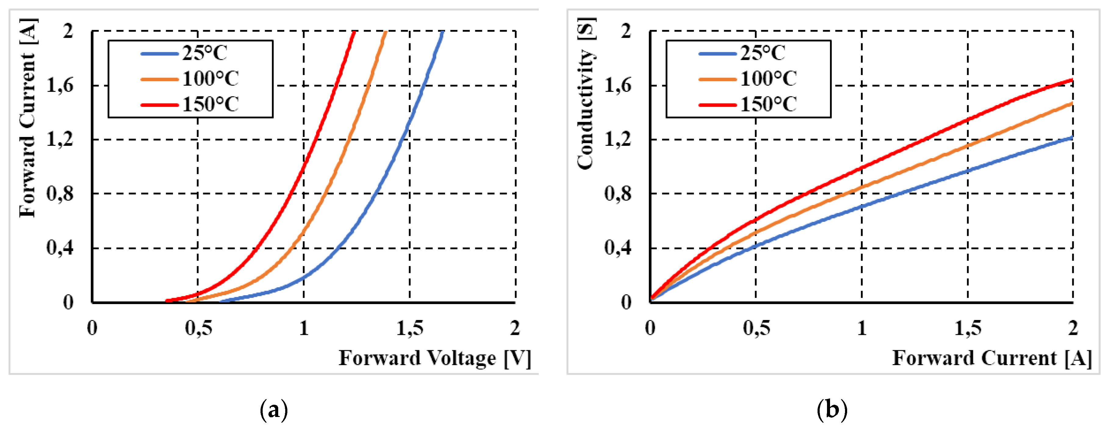
The extracted VA characteristic from the datasheet of US1MHE3 [
24] can be seen in
Figure 7a, while temperature dependency for 25 (°C), 100 (°C), and 150 (°C) is considered. The
Figure 7b corresponds with the temperature dependency of the conductance characteristics of the given diode. The fourth order approximation of conductivity dependency on forward current corresponds to Equation (14).
- 2.
Thermal Coefficient Determination.
The thermal coefficient is determined for temperature interval from 25 (°C) to 150 (°C) and its dependency can be seen in
Figure 8. The fourth order approximation of thermal coefficient “
kT” in dependency on forward current corresponds to Equation (15).
- 3.
Package Dimensions + DIE and Bonding size estimation.
The diode´s package dimensions are listed in the datasheet (
Figure 9). The DIE dimensions are estimated based on the similar device in the same package (
Figure 3).
The geometrical parameters of the package (SMA) and estimated geometrical parameters of the DIE that are used in the simulation model can be seen in
Table 4.
- 4.
Preliminary Simulation Model and Conductivity Coefficient determination.
The results from the preliminary simulation model using settings described in previous sections can be seen in
Figure 10. From these results, it is possible to determine the conductivity coefficient as in (16) and (17).
- 5.
New conductivity characteristic and simulation model comparison.
The received conductivity characteristic using the previously described procedures defined by Equation (18):
The accuracy of this approach is evaluated by comparison of the simulated volt–ampere characteristic (VA) characteristics with VA characteristics given by the datasheet, while temperature dependency is considered as well (
Figure 11). For a given range of diode forward current, we can say that from an electrical point of view, the relative error of the proposed model is less than 1% for 25 °C characteristic, less than 2% for 100 °C characteristic, and less than 5% for 150 °C characteristic.
Main difference is recorded for high operational temperature, i.e., 150 degrees. This level of the operational temperature represents limiting value of the Si semiconductor technology, while electro-thermal process and non-linear dependencies are potentially much higher compared to lower temperatures. Therefore, the highest difference is achieved for potentially the highest allowed operational temperature.
5. Comparisons of Simulation Results with Experimental Measurements
The proposed simulation model is verified for different current values (during steady state operation), while received results were compared with the results from experimental measurement (
Figure 12).
The investigation of operation within experiments was performed by way of implementation of the selected diode, within the main circuit of DC-DC converter (boost type). The three different diode currents were set having the same RMS values as within simulation). Thermal behavior of the diode was evaluated with the use of the FLIR SC600 thermal camera. The input/output parameters of the converter circuit are listed in
Table 5.
The experimental setup is shown in
Figure 12. The diode voltage and current were measured by the current and voltage probe while time-waveforms were visualized on the digital oscilloscope. The input and output voltages and currents were measured with a precise power analyzer, while the individual settings reflected simulation conditions.
The experiments were made based on the experimental set-up described above. The focus was given on infrared thermo-vision measurements of the selected power diode.
Figure 13a shows the temperature distribution within the surface of the investigated component indicating a hot spot during the experimental measurement. This point is located in the space where a silicon power chip is integrated within the diode package. As can be seen, the maximum temperature for the situation of I
F(RMS) = 300 mA has reached approximately 120 °C.
Simultaneously, to verify the electro-thermal behavior of the simulation model,
Figure 13b shows the result of the simulation analysis. The evaluation of the temperature at the hot spot of the component shows that the maximum reached during simulation is 119.4 °C. This value is very close to the result, which was reached during measurement, and it is seen that temperature distribution is similar comparing both results. The relative error for this value of current represents −0.5%.
Measurement valid for the second value of the diode´s current is shown in
Figure 14, while I
F(RMS) = 410 mA. The temperature distribution within the diode package is the same as for the previous situation, while the maximum reached temperature value is 152 °C in the case of measurement (
Figure 14a). Simulation analysis was performed at given conditions according to the second measurement, and results are seen in
Figure 14b. The hot spot, in this case, reached 153.43 °C, thus representing a relative error during this situation on the level of 0.94%.
Because the operational maximum of selected power diode, from the thermal performance point of view, is defined as 150 °C, the last experiment was realized for 500 mA. The temperature maximum is defined for the body of the diode; therefore, even though the temperature reached 152 °C within the previous experiment, it must be noted here that the device temperature, considering the whole volume, is around 100 °C.
Figure 15a shows thermal distribution during measurement for I
F(RMS) = 500 mA. The temperature hot spot reached over 192 °C and this point represents the maximum operational limit considering the temperature of the device. Consequently, a simulation experiment was performed for the last value of forward current. The results are shown in
Figure 15b, while it is seen that the hot spot reached a maximum temperature at the value of 183.67 °C. This last comparison represents the highest relative error (−4.3%) from individual experiments. This is closely related to the V-A characteristic at 150 °C shown in
Figure 12, where it is seen that the shape of the characteristic between measurement and simulation represents the highest deviation.
6. Conclusions
The paper presents a modelling approach based on the indirect identification of key variables required for electro-thermal simulation of semiconductor devices. The design procedure of the semiconductor diode is discussed here. Initially, the geometrical model within the CFD software (COMSOL) was realized based on the X-ray frames received by the manufacturer. The definitions of the geometrical parameters given within the paper show how it is possible to prepare a fully reconfigurable simulation model. Individual parameters of the geometrical part are then related to the physical properties of the model. After this, the identification of the parameters, which influence the temperature performance of the component, was provided, i.e., physical variables like conductivities of individual component´s subdomains were identified. The procedure of the parameter identifications is indirect, i.e., the designer does not need to receive material properties defined by the manufacturer [
14]. The proposed methodology uses identification based on V-A diode characteristics. The validation of the proposed model accuracy and validity was evaluated by the results received from the experimental measurement. The evaluation was based on an investigation of temperature distribution within the component surface for various operational conditions considering different power loading of the component. After evaluation, it was found that the relative error between results from simulation and measurements varies from 0.94 % to −4.3%. This difference is dependent on the amount of the forward current flowing through the diode. Increased error reported at the end of the paper were caused by the unspecified structural component changes at higher temperatures. Generally, it can be concluded that the presented approach represents a perspective way of electro-thermal modeling of semiconductor components, thus eliminating the need for the use of semiconductor physics during the development of simulation models. Moreover, it enables the improvement of computation time, maintaining adequate accuracy and performance of simulation model.
Finally, it is important to note that existing methods for thermal field identification require mostly estimation of power dissipation within the given component. In other words, a designer needs to calculate power losses for each of the operational conditions to receive results of thermal performance for a wide operational range (transient or steady state). The presented method, does not require recalculations of the power dissipation, because the model uses electro-thermal domain, and automated–indirect extraction of required variables to identify thermal field distribution. Based on the presented approach more flexibility related to the automated calculation process should be obtained. Moreover, the presented modelling approach enables the analysis of electronic components in transient as well as in steady-state operations dynamically, without the need to look-up the table of power dissipation required for various conditions.
Author Contributions
Conceptualization, methodology, writing—original draft preparation, and funding acquisition, M.F., software, validation, and investigation M.P. All authors have read and agreed to the published version of the manuscript.
Funding
This research was funded by National Grant Agency Vega, grant number 1/0063/21 and by National Grant Agency APVV for project funding APVV-17-0218.
Institutional Review Board Statement
Not applicable.
Informed Consent Statement
Not applicable.
Data Availability Statement
Not applicable.
Acknowledgments
The authors wish to thank for the support to the Slovak grant agency Vega for project no. 1/0063/21.
Conflicts of Interest
The authors declare no conflict of interest.
References
- Vakrilov, N.; Stoyanva, A.; Bonev, B. 3D Thermal Modelling and Verification of Power Electronic Modules. In Proceedings of the 42nd International Spring Seminar on Electronics Technology (ISSE), Wroclaw, Poland, 15–19 May 2019; pp. 1–4. [Google Scholar] [CrossRef]
- Frivaldsky, M.; Spanik, P.; Drgona, P.; Loncova, Z. Algorithms for indirect investigation of heat distribution in electronic systems. Int. J. Therm. Sci. 2016, 114, 15–34. [Google Scholar] [CrossRef]
- Valdovinos, M.S. Energy and concentration nonequilibrium and nonlinear charge transport phenomena in semiconductors in a magnetic field in hot electrons approximation. Int. J. Therm. Sci. 2018, 137, 110–120. [Google Scholar] [CrossRef]
- Spanik, P.; Cuntala, J.; Frivaldsky, M.; Drgona, P. Investigation of Heat Transfer of Electronic System through Utilization of Novel Computation Algorithms. Elektron. Ir Elektrotechnika 2012, 123, 31–36. [Google Scholar] [CrossRef] [Green Version]
- Rafajdus, P.; Peniak, A.; Dubravka, P. Optimization of Switched Reluctance Motor Design Procedure for Electrical Vehicles. In Proceedings of the International Conference on Optimization of Electrical and Electronic Equipment (OPTIM), Bran, Romania, 22–24 May 2014; pp. 1–4. [Google Scholar] [CrossRef]
- Wang, Z.; Tian, X.; Liang, J.; Zhu, J.; Tang, D.; Xu, K. Prediction and measurement of thermal transport across interfaces between semiconductor and adjacent layers. Int. J. Therm. Sci. 2014, 79, 266–275. [Google Scholar] [CrossRef]
- Eveloy, V.; Lohan, J.; Rodgers, P. A Benchmark Study of Computational Fluid Dynamics Predictive Accuracy for Component-Printed Circuit Board Heat Transfer. IEEE Trans. Compon. Packag. Technol. 2000, 23, 568–576. [Google Scholar] [CrossRef]
- Ammous, A.; Sellami, F.; Ammous, K.; Morel, H.; Allard, B.; Chante, J.P. Developing an equivalent thermal model for discrete semiconductor packages. Int. J. Therm. Sci. 2003, 23, 266–275. [Google Scholar] [CrossRef]
- Tatchell, D.; Parry, J.; Clark, I. Advances in Cooling Electronics with CFD. In Proceedings of the NAFEMS World Congress, Salzburg, Austria, 10–12 June 2013. [Google Scholar]
- Koniar, D.; Hargas, L.; Stofan, S. High Speed Video System for Tissue Measurement Based on PWM Regulated Dimming and Virtual Instrumentation. Elektron. Ir Elektrotechnika 2010, 10, 169–172. [Google Scholar]
- Ayadi, M.; Fakfakh, M.A.; Ghariani, M.; Neji, R. Developing an equivalent thermal model for discrete DIODE packages. Int. J. Therm. Sci. 2011, 50, 1484–1491. [Google Scholar] [CrossRef]
- Andonova, A.; Kim, N.; Vakrilov, N. Estimation the amount of heat generated by LEDs under different operating conditions. Elektron. Ir Elektrotechnika 2016, 22, 49–53. [Google Scholar] [CrossRef]
- Mashayekhi, R.; Khodabandeh, E.; Akbari, O.A.; Toghraie, D.; Bahiraei, M.; Gholami, M. CFD analysis of thermal and hydrodynamic characteristics of hybrid nanofluid in a new designed sinusoidal double-layered microchannel heat sink. J. Therm. Anal. Calorim. 2018, 134, 2305–2315. [Google Scholar] [CrossRef]
- Hruska, K.; Kindl, V.; Pechanek, R. Design and FEM analyses of an electrically excited automotive synchronous motor. In Proceedings of the 15th International Power Electronics and Motion Control Conference (EPE/PEMC), Novi Sad, Serbia, 4–6 September 2012; pp. LS2e.2-1–LS2e.2-7. [Google Scholar] [CrossRef]
- Kucera, M.; Sebok, M.; Kubis, M.; Korenciak, D.; Gutten, M. Analysis of the Automotive Ignition System for Various Conditions. Commun.-Sci. Lett. Univ. Zilina 2020, 22, 144–152. [Google Scholar] [CrossRef]
- Staliulionis, Z.; Zhang, Z.; Pittini, R.; Andersen, M.A.E.; Noreika, A.; Tarvydas, P. Thermal Modelling and Design of On-board DC-DC Power Converter using Finite Element Method. Elektron. Ir Elektrotechnika 2014, 20, 38–44. [Google Scholar] [CrossRef] [Green Version]
- Nobile, G.; Cacciato, M.; Scarcella, G.; Scelba, G. Multi-Criteria Experimental Comparison of Batteries Circuital Models for Automotive Applications. Commun.-Sci. Lett. Univ. Zilina 2018, 20, 97–104. [Google Scholar]
- Kascak, S.; Prazenica, M.; Jarabicova, M.; Paskala, M. Interleaved DC/DC Boost Converter with Coupled Inductors. Adv. Electr. Electron. Eng. 2018, 16, 147–154. [Google Scholar] [CrossRef]
- Frivaldsky, M.; Donic, T.; Vavrus, V.; Pavelek, M. Experimental research of optimization methodology for local, resistive-heating of thin molybdenum plates. Int. J. Therm. Sci. 2017, 121, 111–123. [Google Scholar] [CrossRef]
- Hockicko, P.; Bury, P.; Munoz, F. Investigation of relaxation and transport processes in LIPO(N) glasses. J. Non-Cryst. Solids 2013, 363, 140–146. [Google Scholar] [CrossRef]
- Kascak, S.; Resutik, P. Method for estimation of power losses and thermal distribution in power converters. Electr. Eng. 2021, 1–12. [Google Scholar] [CrossRef]
- Zavrel, M.; Kindl, V.; Kavalír, T.; Drabek, P. Design and Construction of High-Quality Capacitor for High Frequency and Power Application. Commun.-Sci. Lett. Univ. Zilina 2018, 23, C1–C6. [Google Scholar] [CrossRef]
- Hockicko, P.; Kudelcik, J.; Munoz, F.; Munoz-Senovilla, L. Structural and electrical properties of LIPO3 Glasses. Adv. Electr. Electron. Eng. 2015, 13, 198–205. [Google Scholar] [CrossRef]
- US1MHE3-61T Datasheet—Vishaz Siliconix. Available online: vhttps://www.googleadservices.com/pagead/aclk?sa=L&ai=DChcSEwjS7cTdrfz0AhWButUKHaqMAygYABAAGgJ3cw&ae=2&ohost=www.google.com&cid=CAASEuRooSqOxyr_e6iByfNUFAkFuw&sig=AOD64_04IojJYKQHeBYAxSozhWlT2q4cyA&q&adurl&ved=2ahUKEwiN0brdrfz0AhVpSfEDHYYBA60Q0Qx6BAgCEAE (accessed on 15 May 2021).
| Publisher’s Note: MDPI stays neutral with regard to jurisdictional claims in published maps and institutional affiliations. |
© 2021 by the authors. Licensee MDPI, Basel, Switzerland. This article is an open access article distributed under the terms and conditions of the Creative Commons Attribution (CC BY) license (https://creativecommons.org/licenses/by/4.0/).


