
Research on Reactive Power Optimization Control of a Series-Resonant Dual-Active-Bridge Converter

Abstract
:1. Introduction
2. Basic Characteristics of the Converter and Reactive Power Analysis
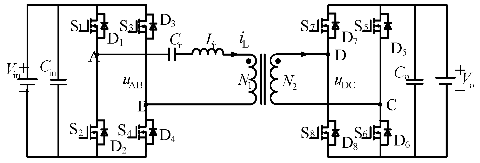
2.1. Introduction of Series-Resonant Dual-Active-Bridge Converter Topology
2.2. Steady-State Mathematical Model under Three Modulation Strategies
- (1)
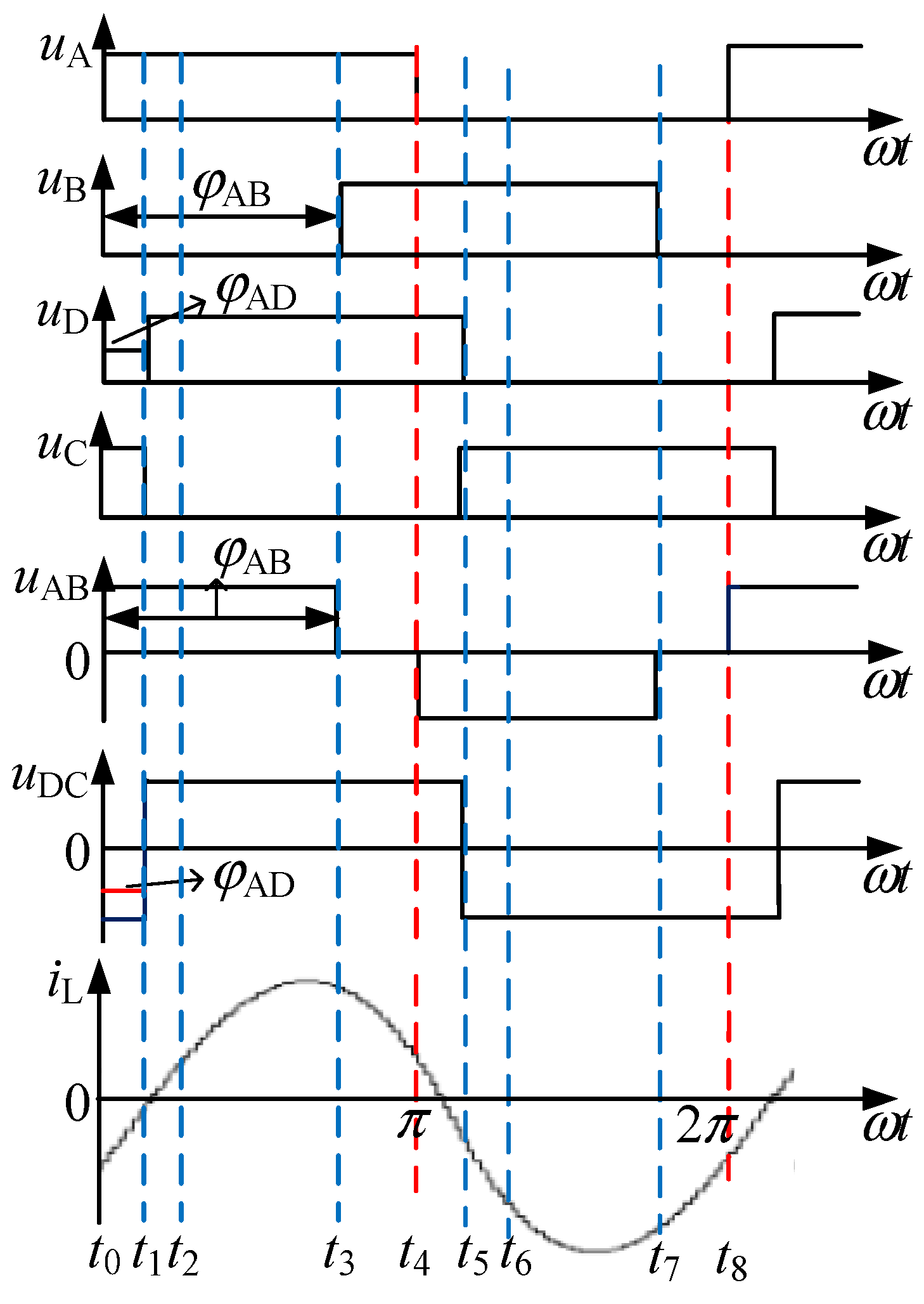
- t0–t1 phase
- (2)
- t1–t2 stage
- (3)
- t2–t3 phase
- (4)
- t3–t4 phase
- (1)
- Phase 1: t0–t1
- (2)
- Phase 2: t1–t2
- (3)
- Stage 3: t2–t3
- (4)
- Stage 4: t3–t4
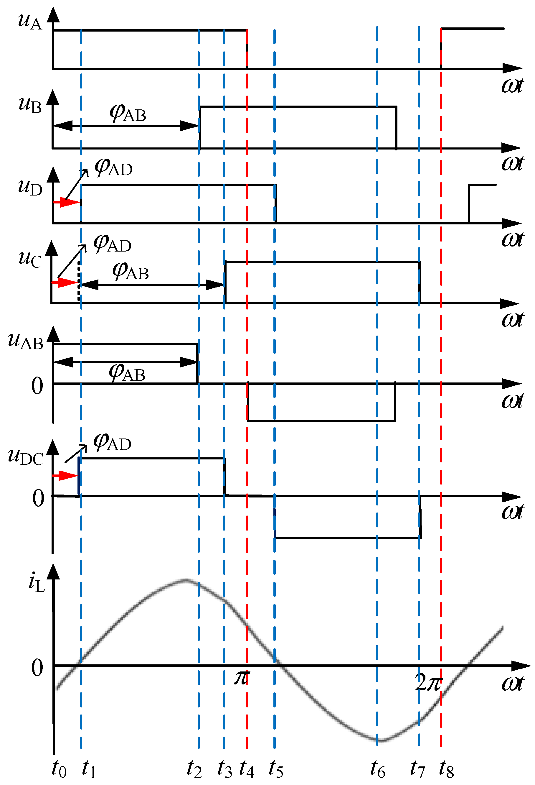
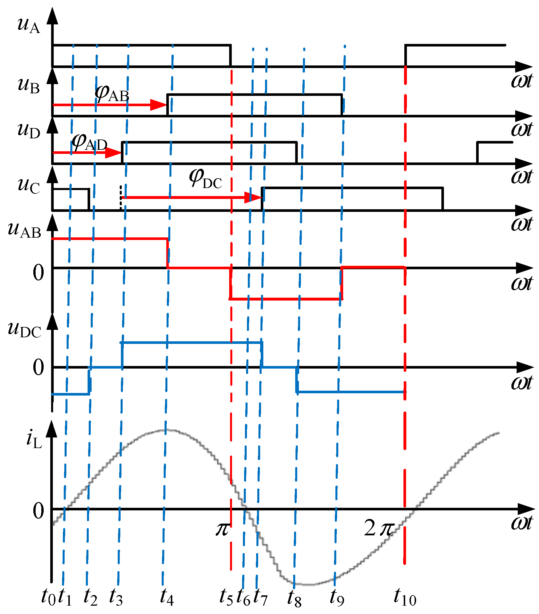
- (1)
- Phase 1: t0–t1
- (2)
- Phase 2: t1–t2
- (3)
- Phase 3: t2–t3
- (4)
- Phase 4: t3–t4
- (5)
- Phase V: t4–t5
2.3. Analysis of Soft-Switching Characteristics under Three Modulation Strategies
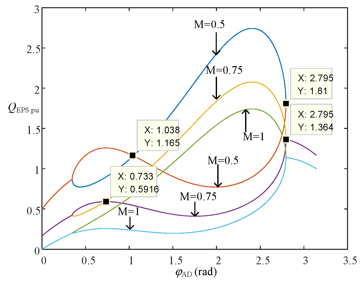
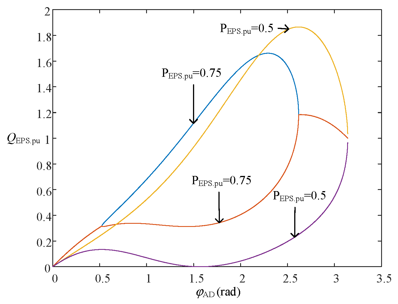
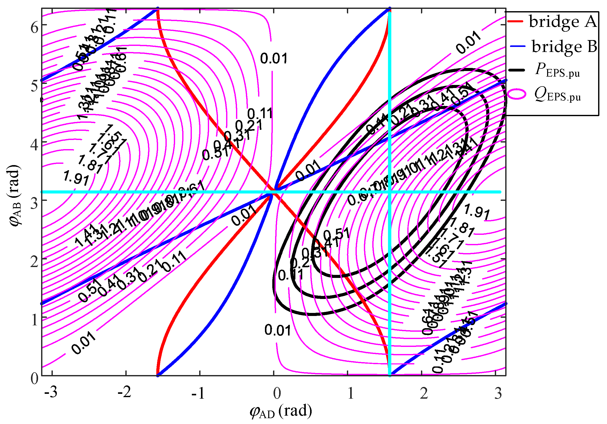
2.4. Minimum Reactive Power Analysis under Different Modulation Strategies
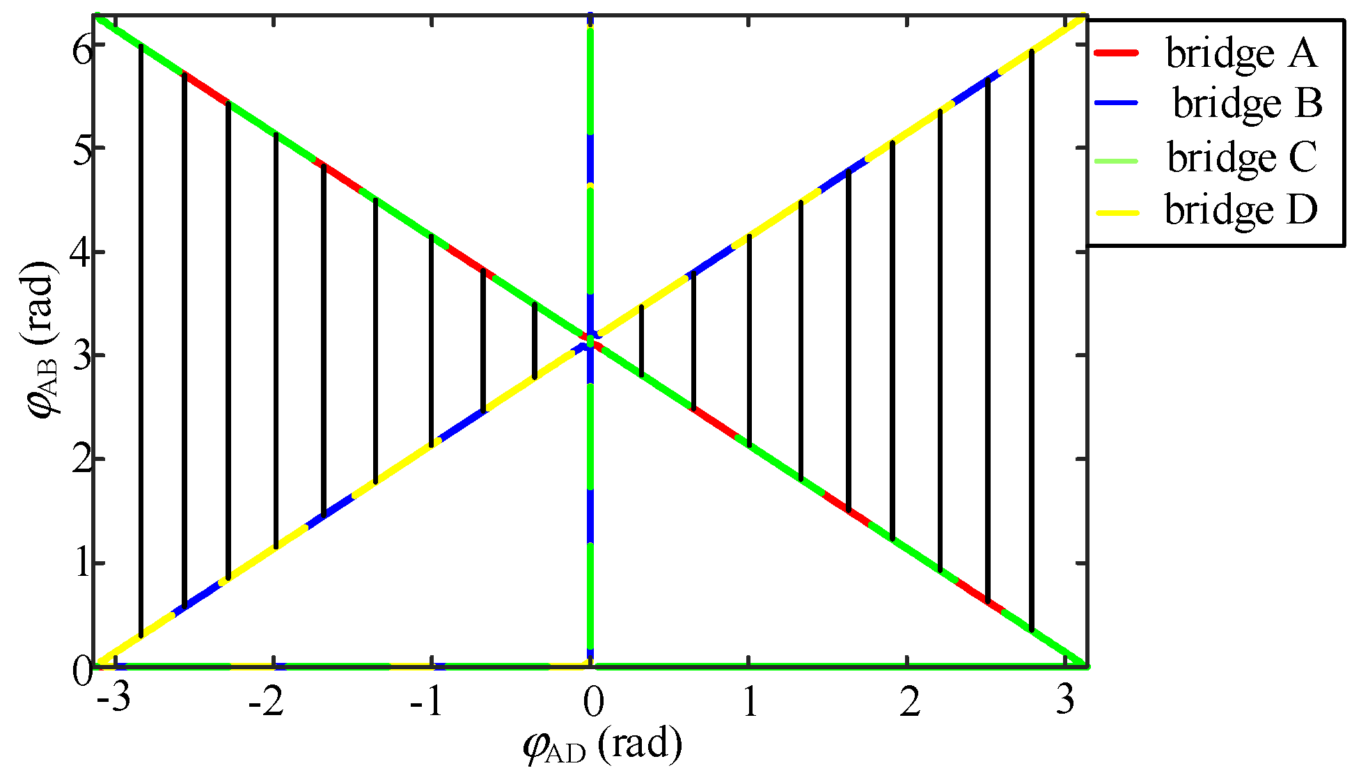
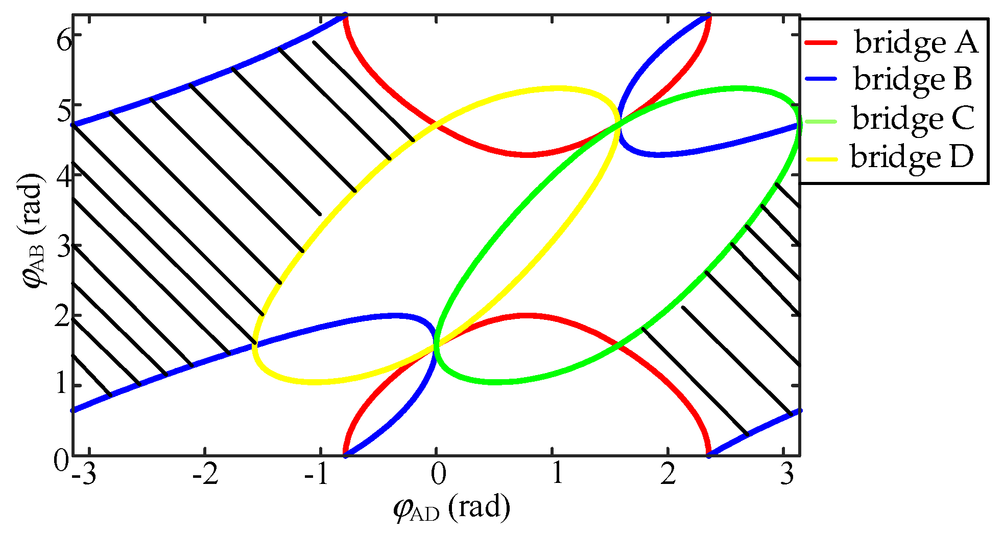
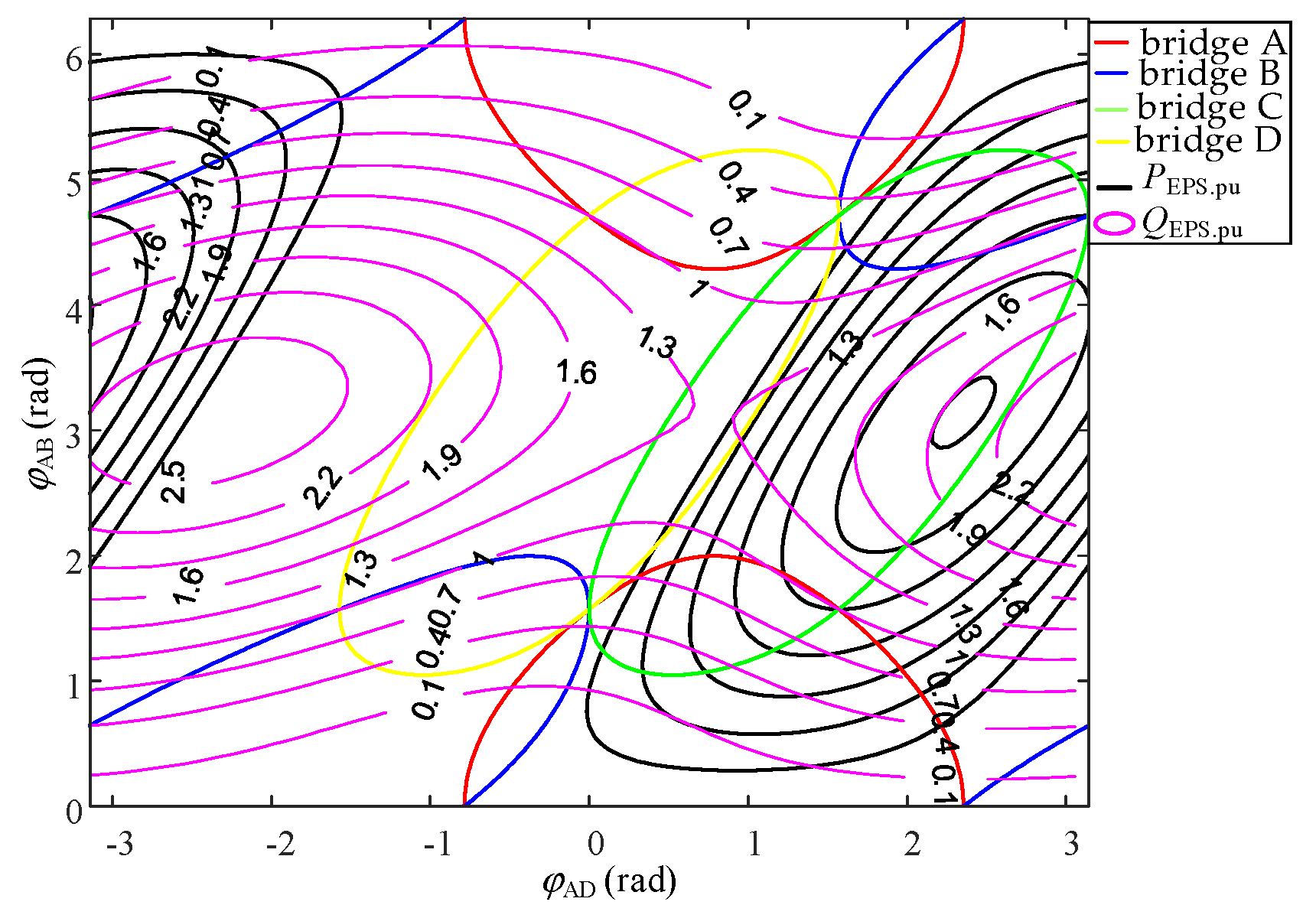
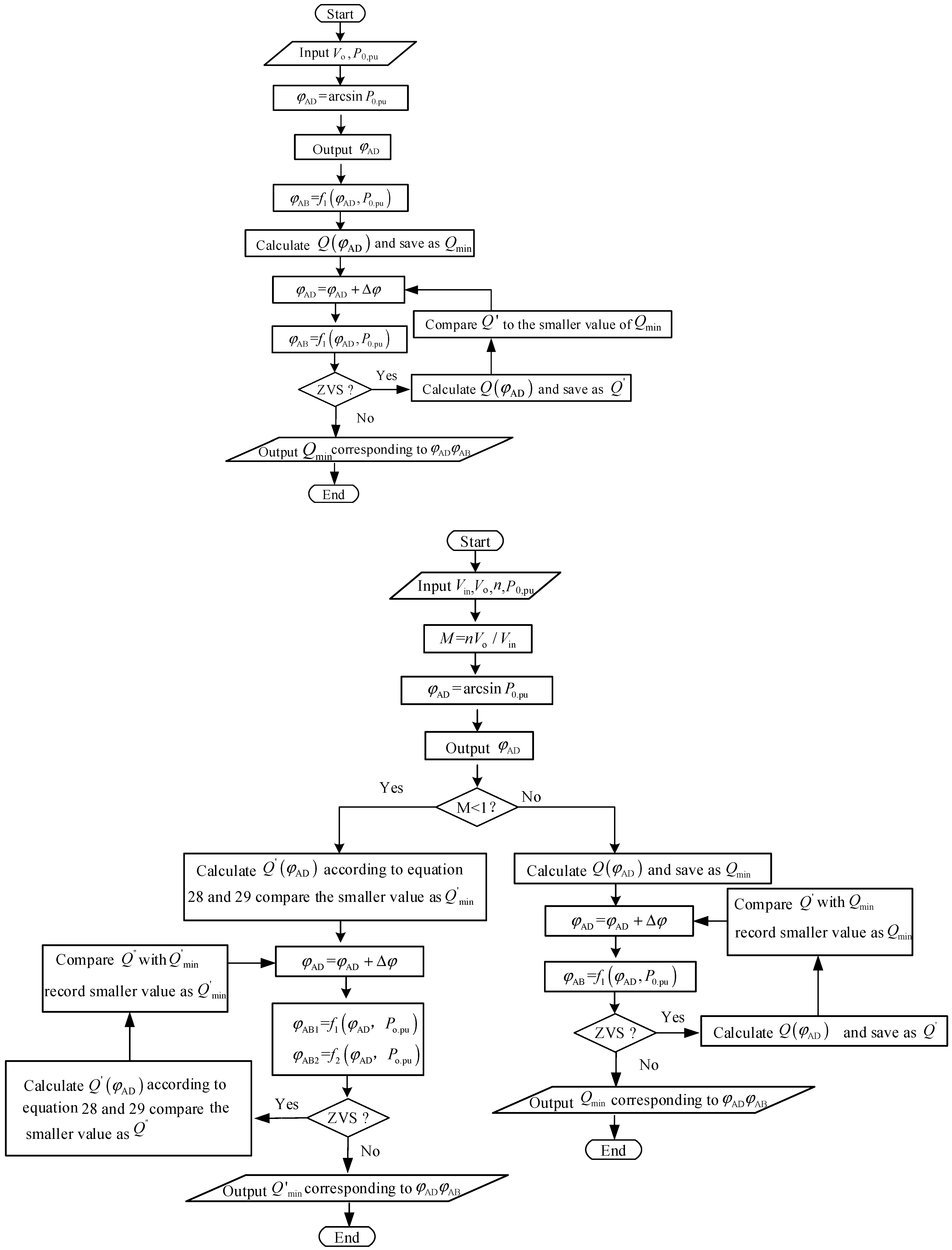
3. Optimal Reactive Power Control Strategy
3.1. Series-Resonant DAB Reactive Power Optimization Control Strategy
- (1)
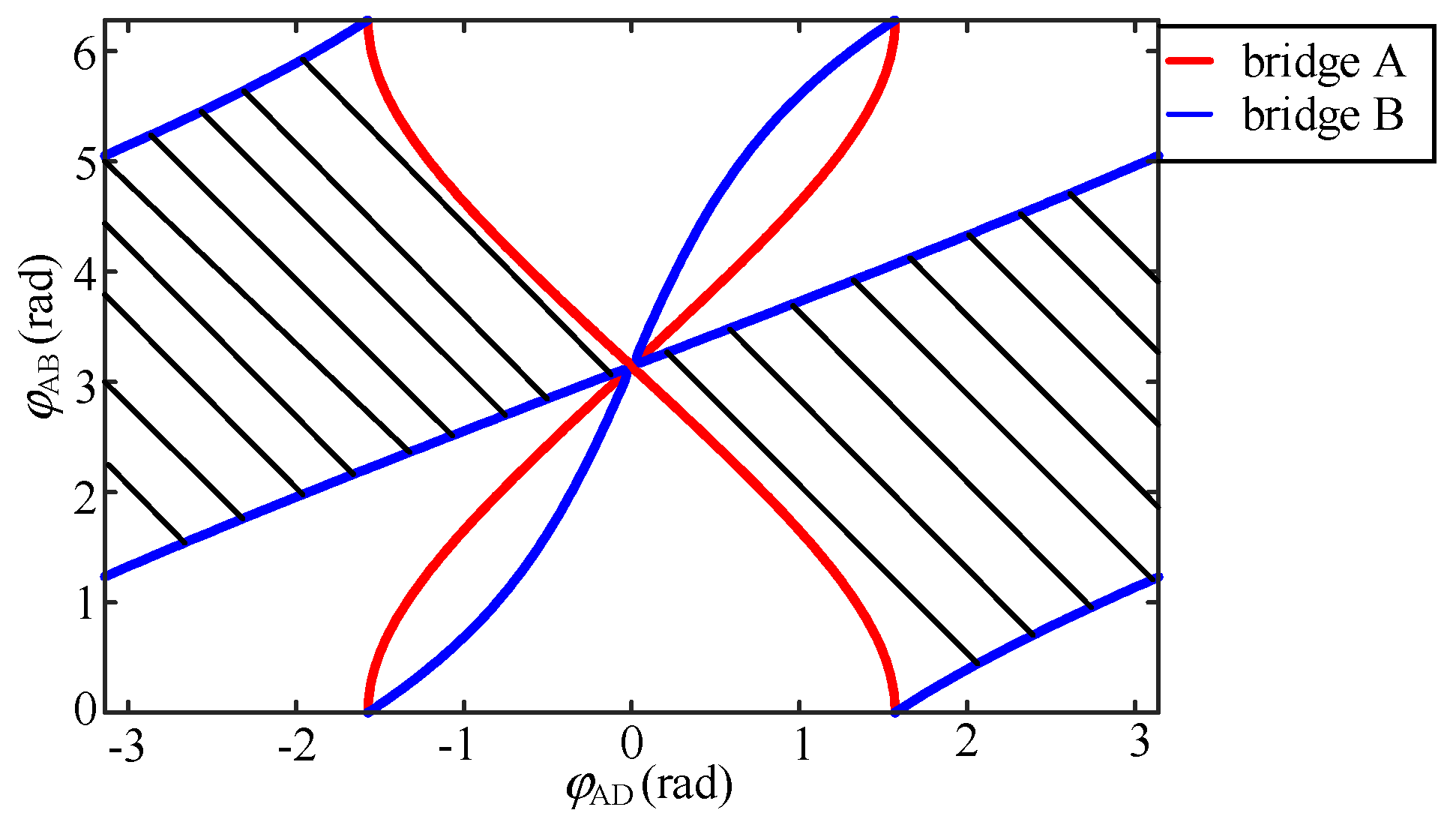
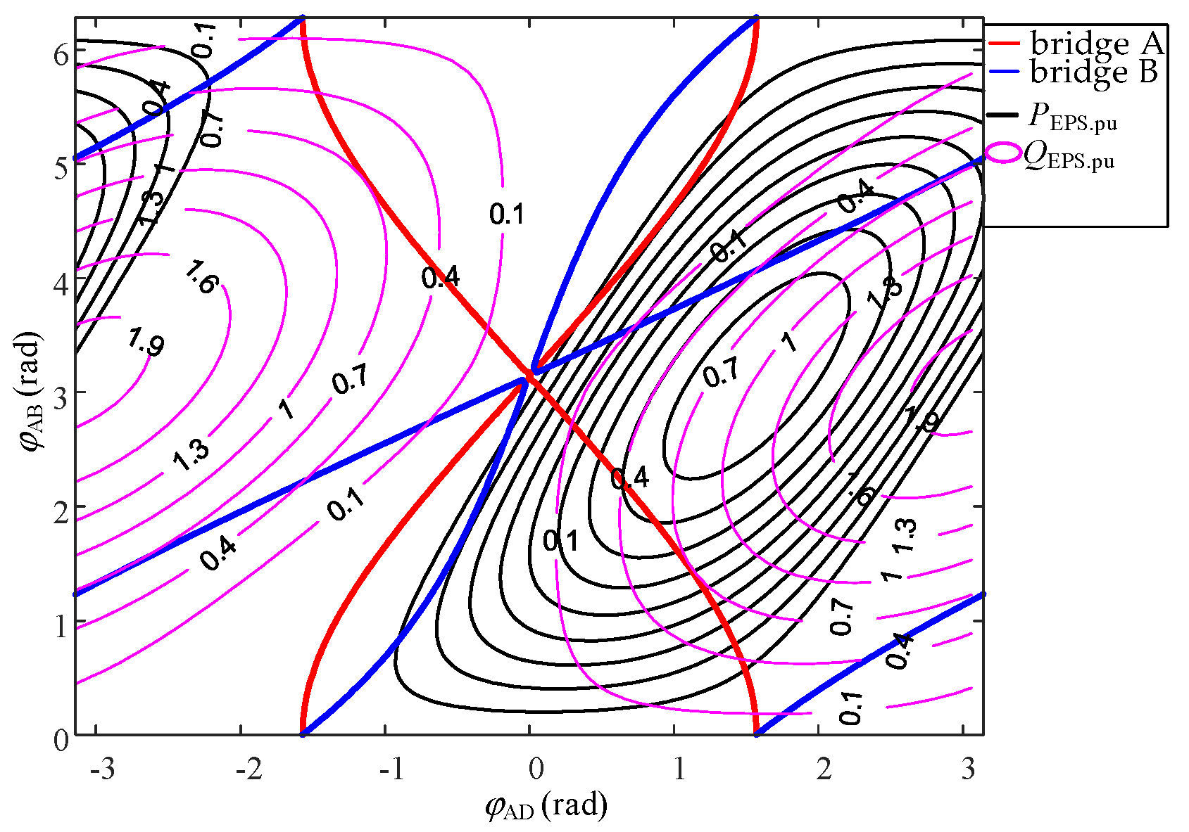
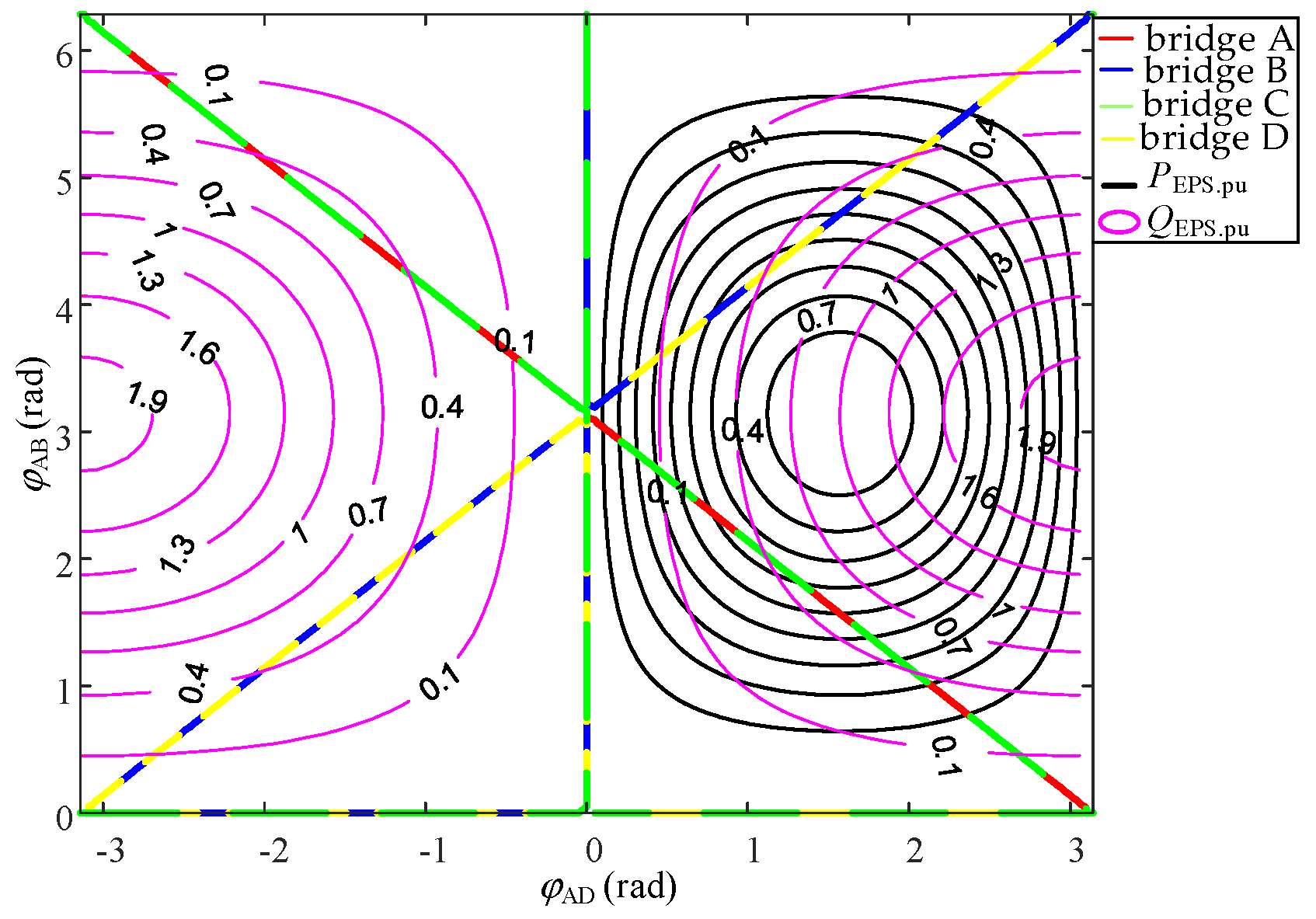
- In a certain active power standardized value, when the same inter-bridge phase-shift angle φAD corresponds to two intra-bridge phase-shift angles φAB and the larger the intra-bridge phase-shift angle, the smaller the value of the reactive power contour is handed over. Similarly, the same intra-bridge phase-shift angle φAB corresponds to two intra-bridge phase-shift angles φAD and the smaller value of the reactive power contour;
- (2)
- At a certain active value in the intersection with the reactive power contour, the closer to the right side of the image, the greater the value of the reactive power; the closer to the left side of the image, the smaller the value of the reactive power;
- (3)
- The minimum reactive power is located in the vicinity of the intra-bridge phase-shift angle φAB = π, which is near the single phase-shift modulation strategy.
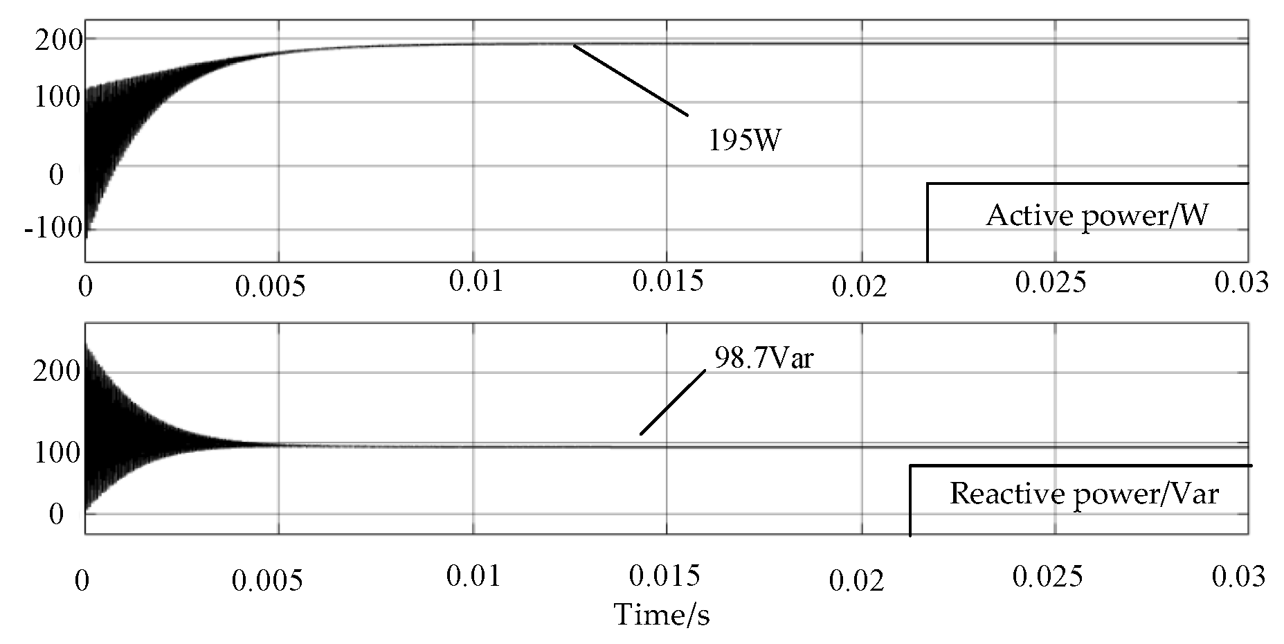
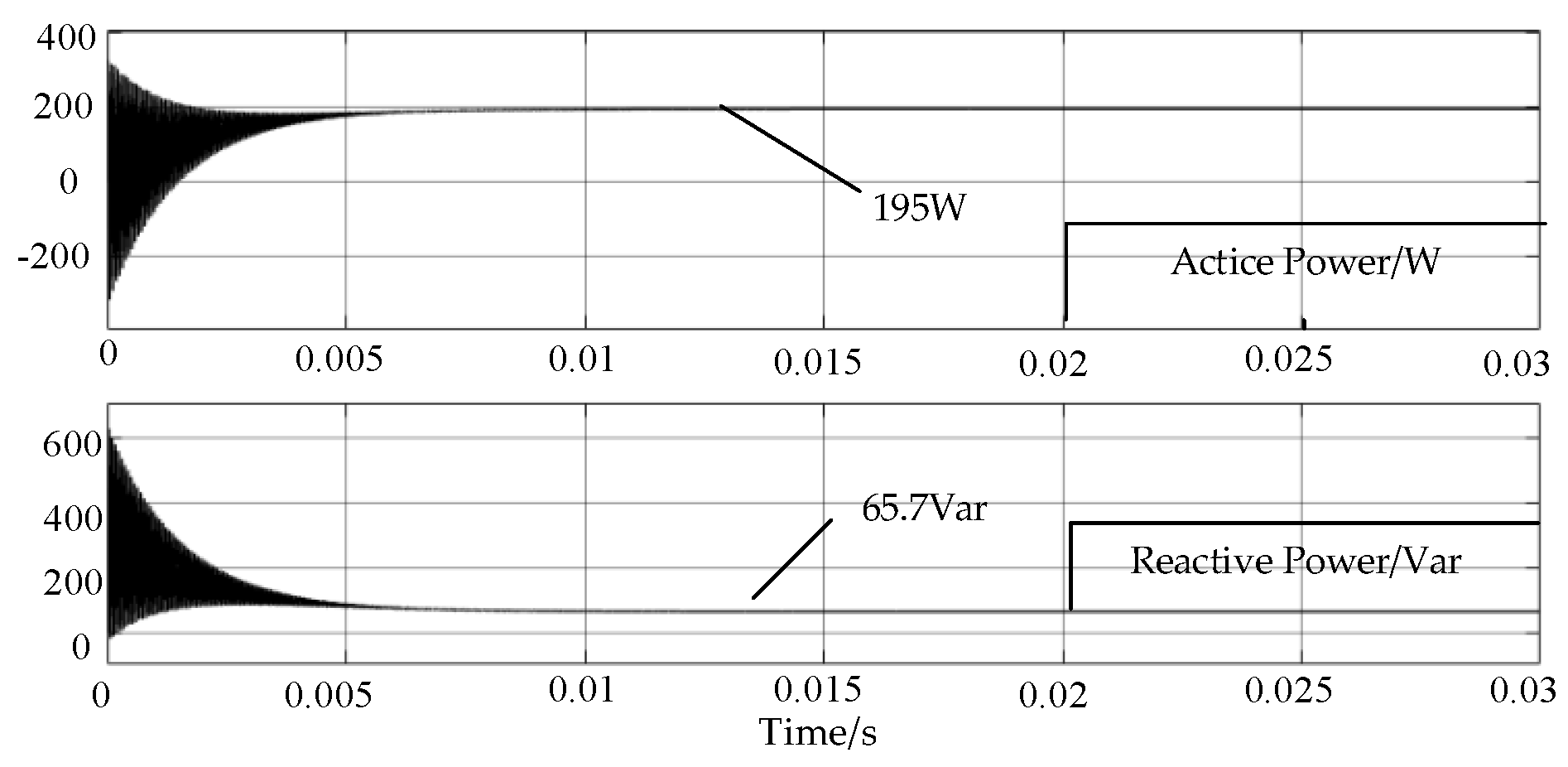
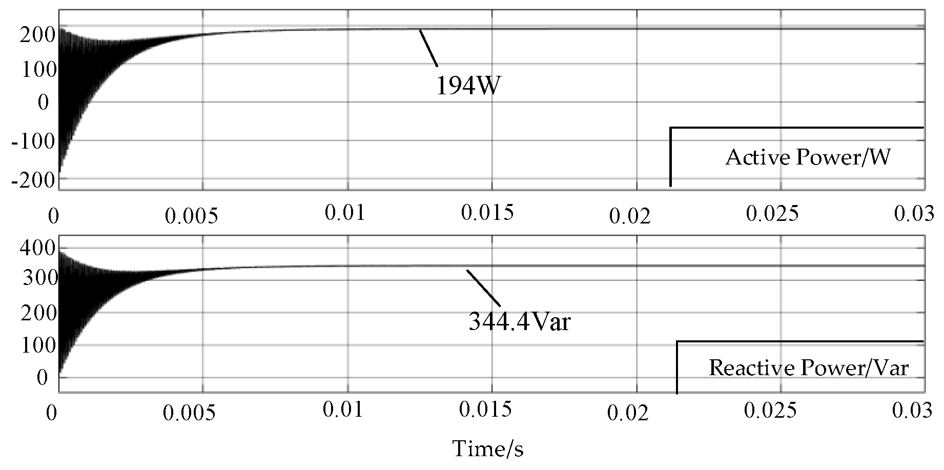
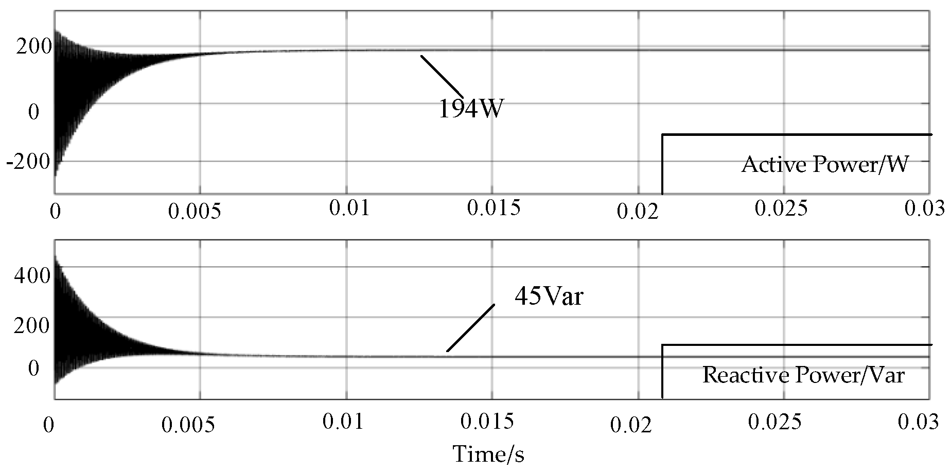
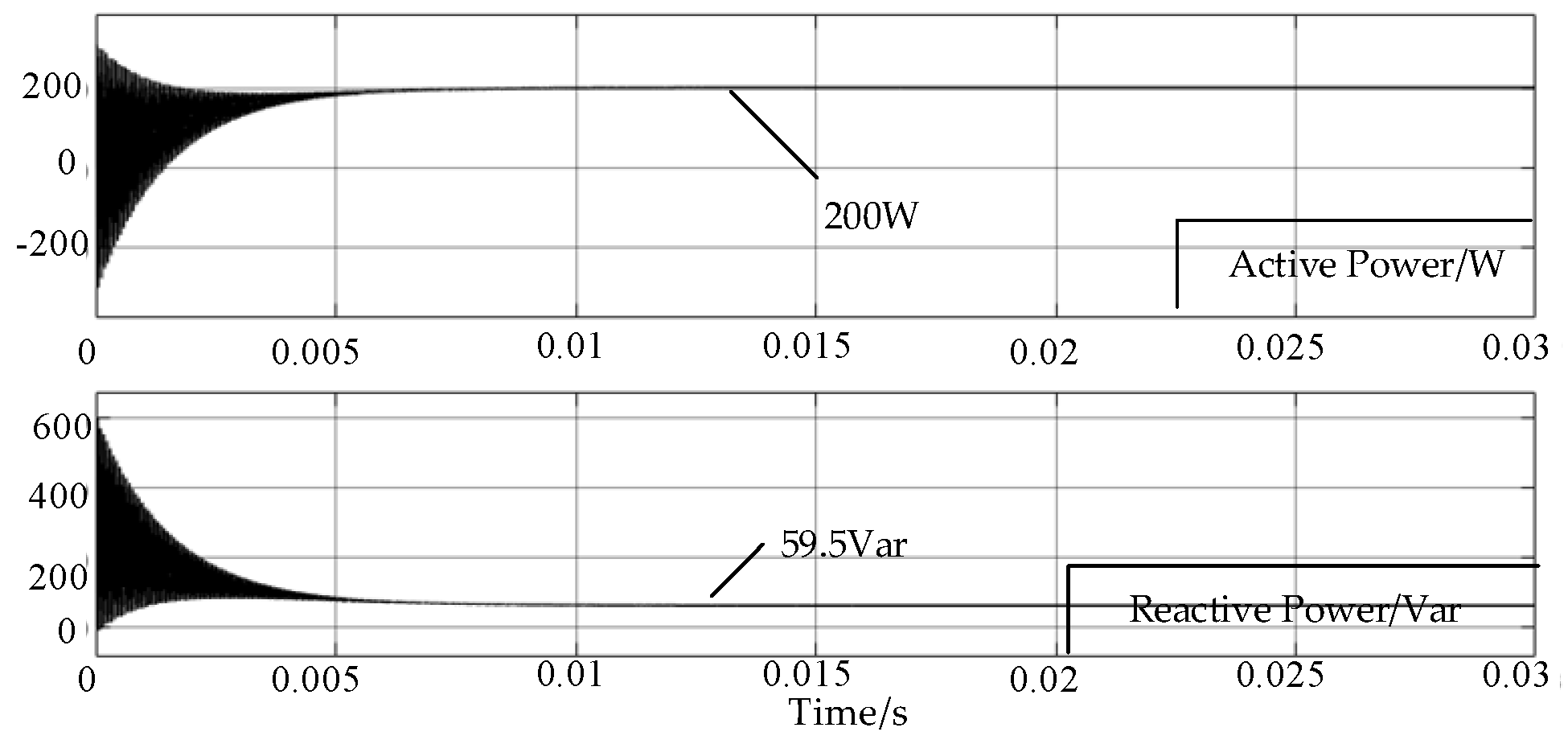
3.2. Minimum Reactive Power Simulation Verification
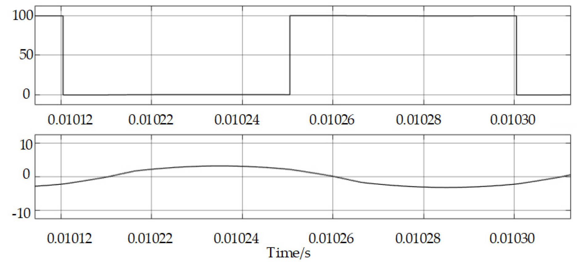
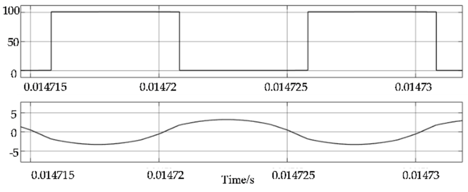
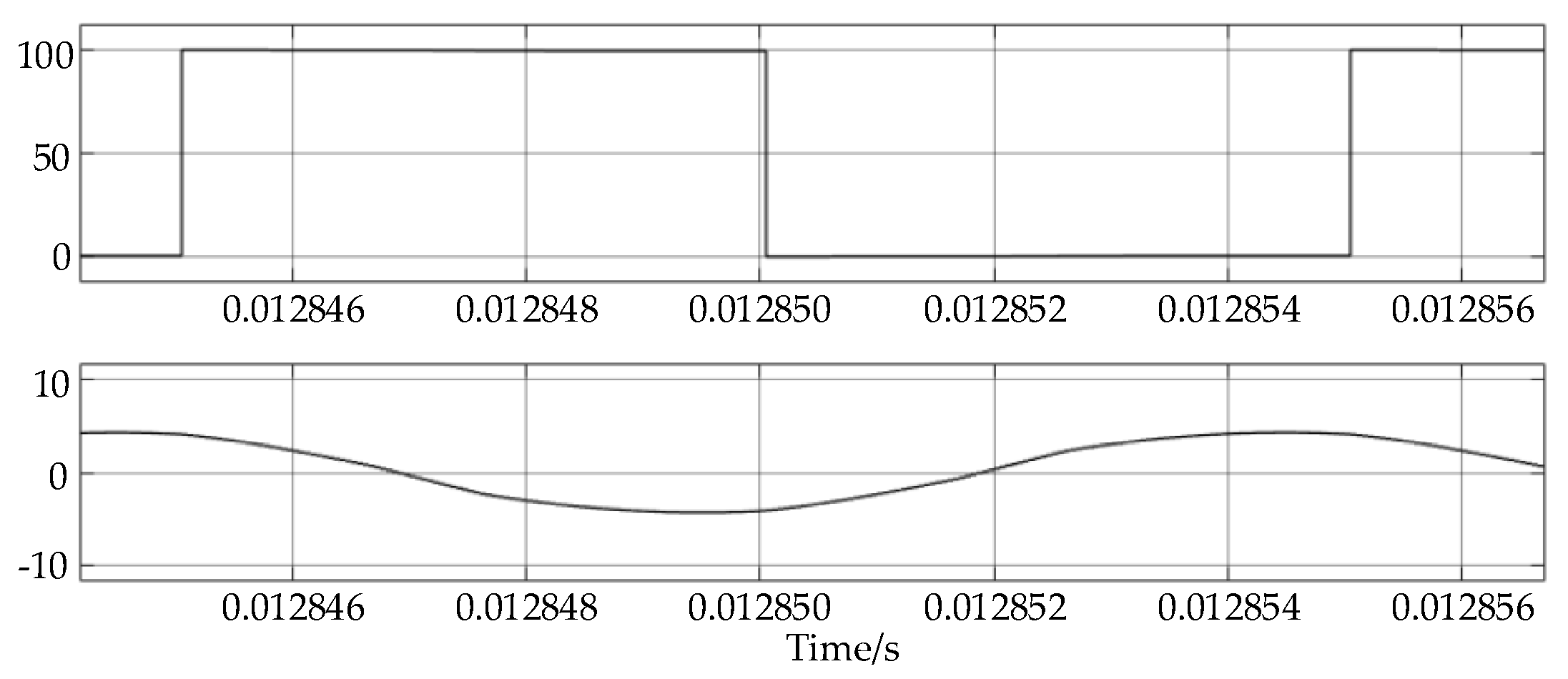
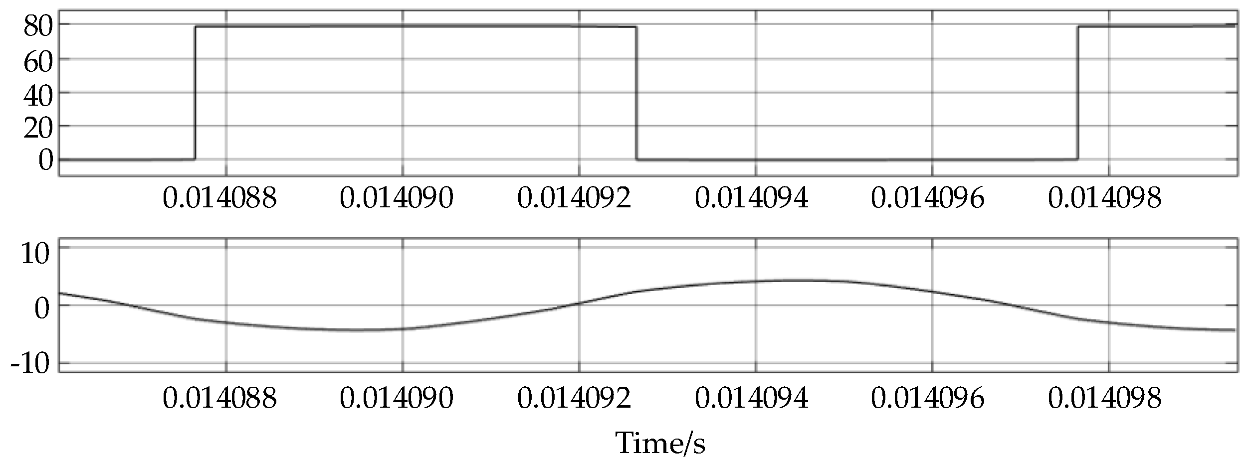
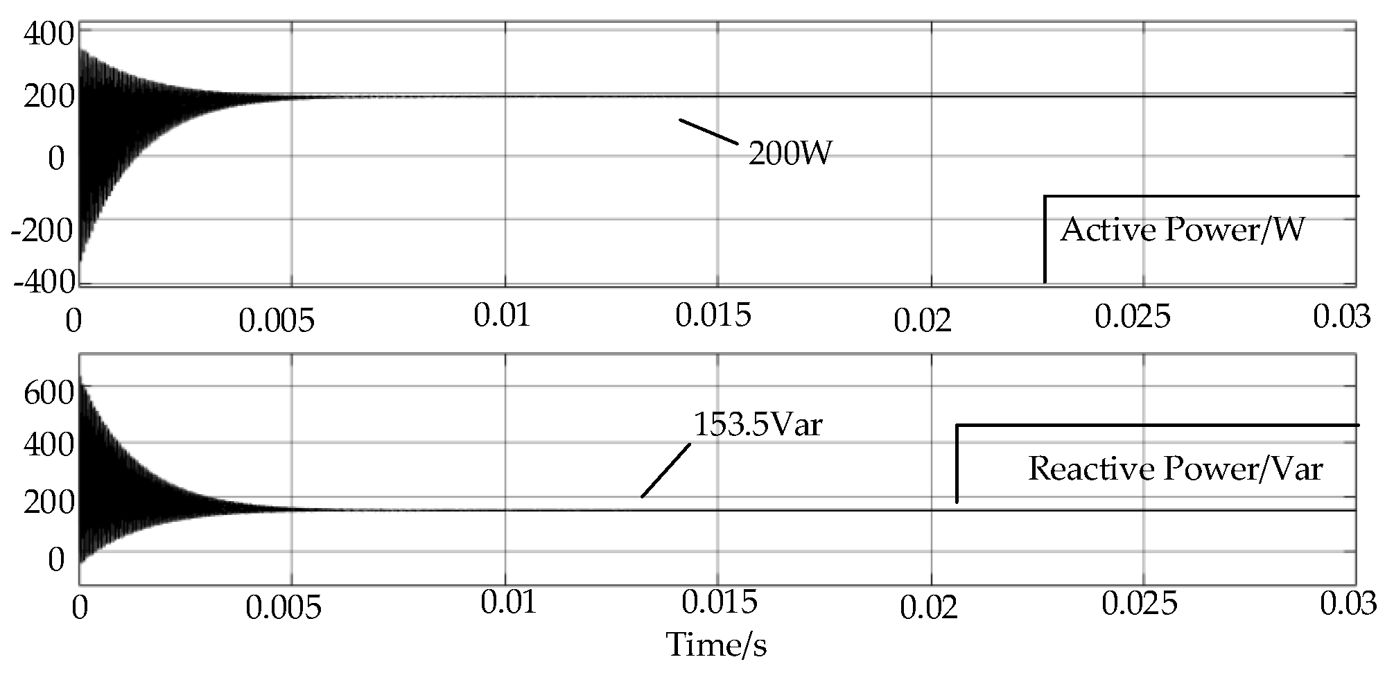
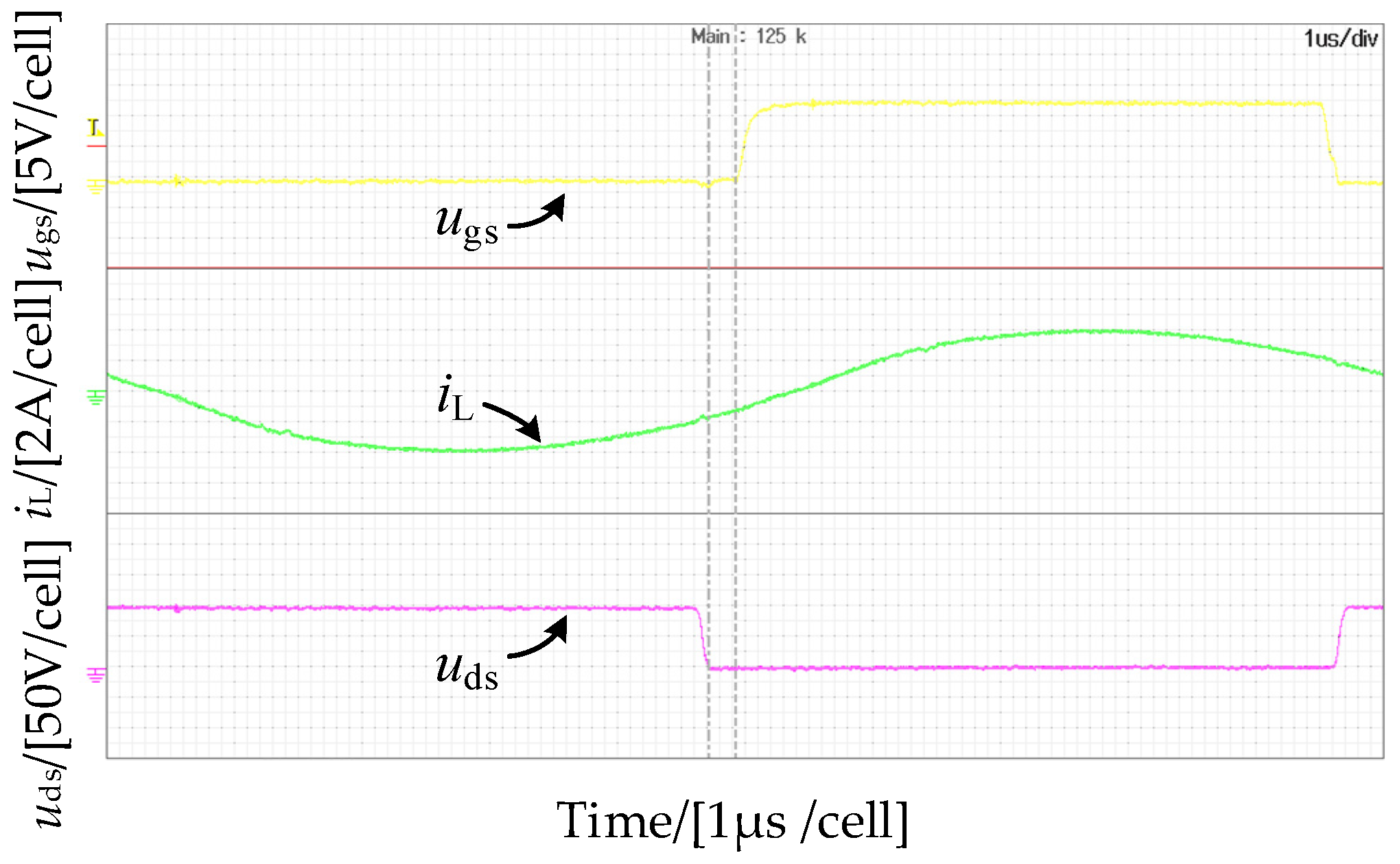
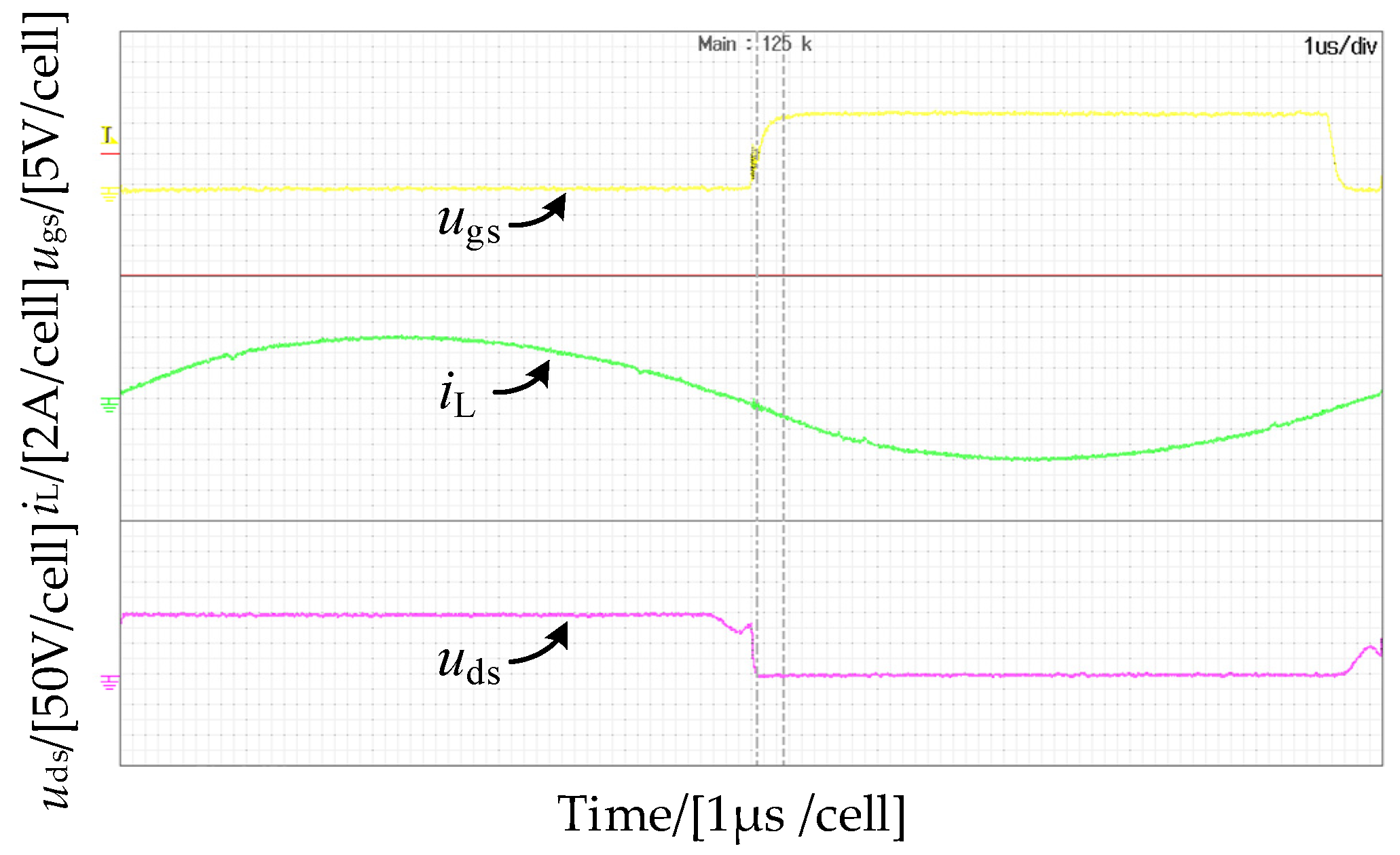
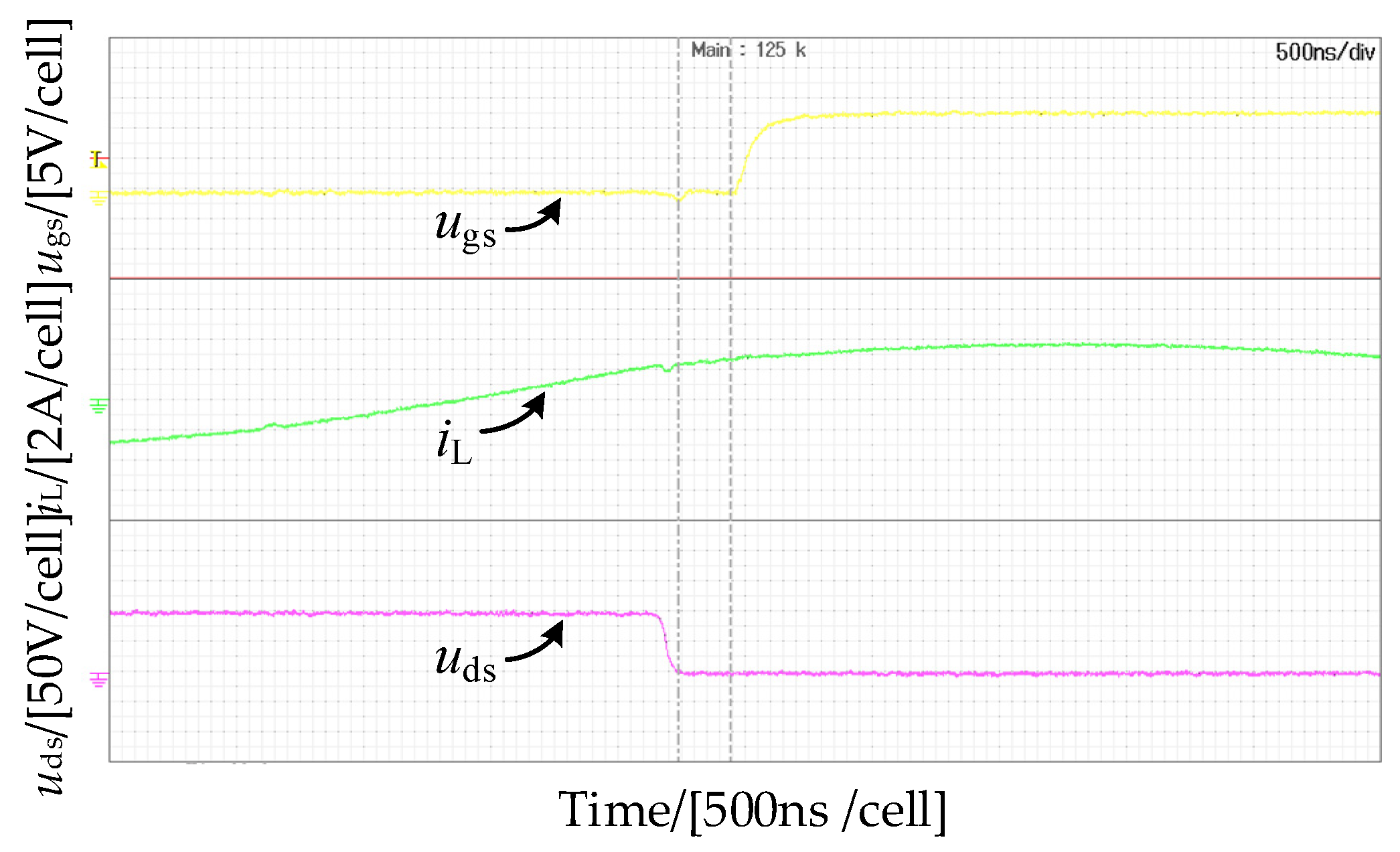
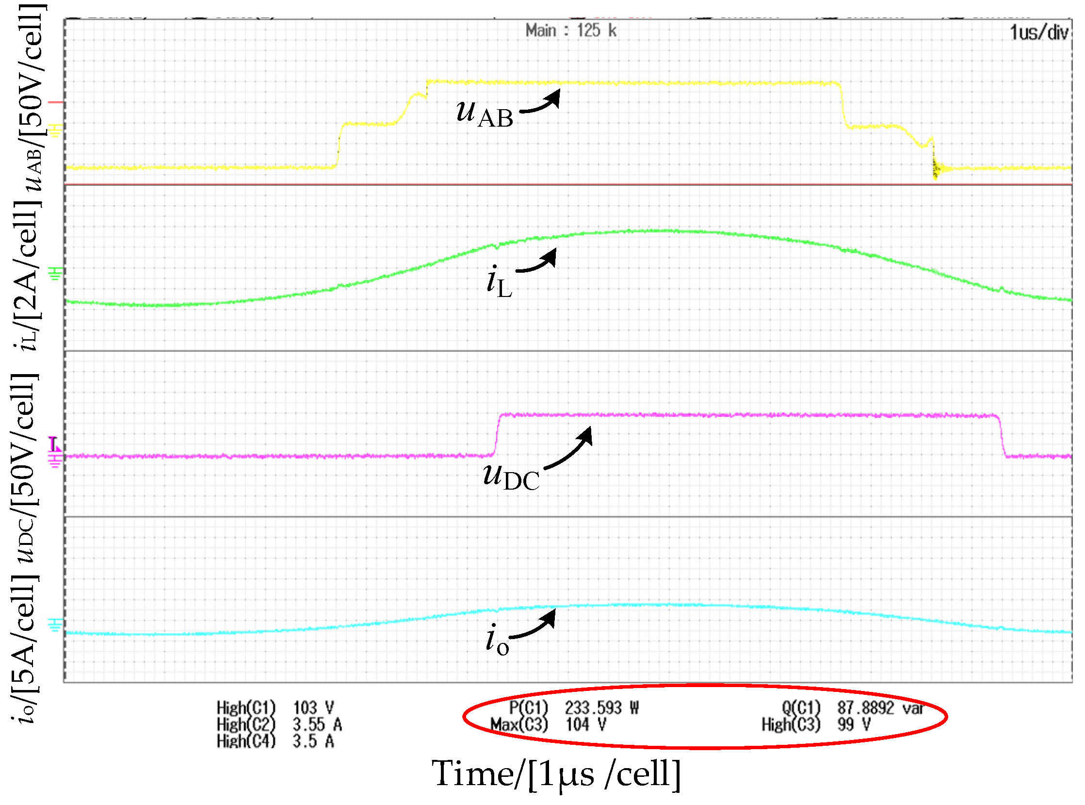
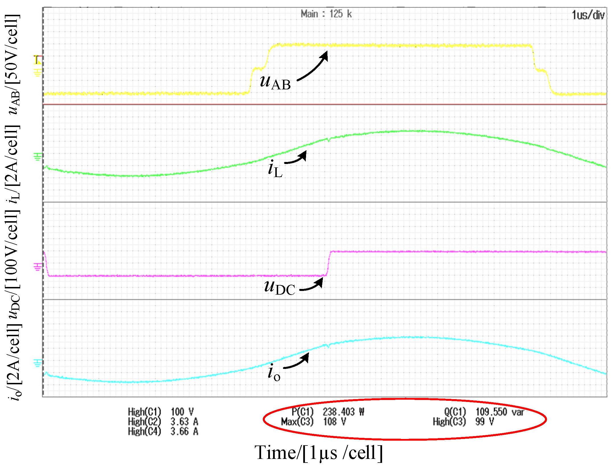
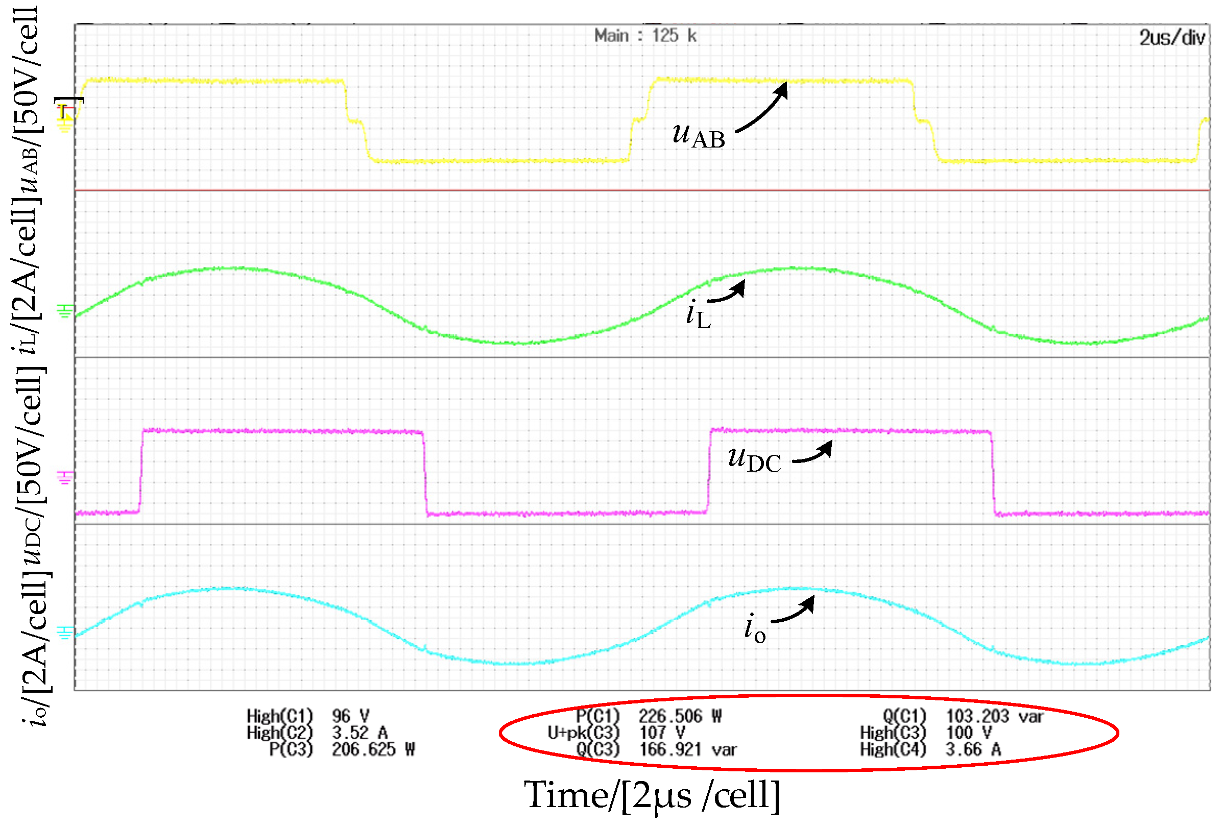
4. Experimental Verification
5. Conclusions
Author Contributions
Funding
Institutional Review Board Statement
Informed Consent Statement
Data Availability Statement
Conflicts of Interest
References
- De Doncker, R.W.; Divan, D.M.; Kheraluwala, M.H. A three-phase soft-switched high-power-density DC/DC converter for high-power applications. IEEE Trans. Ind. Appl. 1991, 27, 63–73. [Google Scholar] [CrossRef]
- Zhao, B.; Song, Q.; Liu, W.; Sun, Y. Dead-Time Effect of the High-Frequency Isolated Bidirectional Full-Bridge DC–DC Converter: Comprehensive Theoretical Analysis and Experimental Verification. IEEE Trans. Power Electron. 2014, 29, 1667–1680. [Google Scholar] [CrossRef]
- Zhao, B.; Yu, Q.; Sun, W. Extended-Phase-Shift Control of Isolated Bidirectional DC–DC Converter for Power Distribution in Microgrid. IEEE Trans. Power Electron. 2012, 27, 4667–4680. [Google Scholar] [CrossRef]
- Verma, V.; Gupta, A. Performance enhancement of the Dual Active Bridge with dual phase shift control and variable frequency modulation. In Proceedings of the IEEE International Conference on Power Electronics, Drives and Energy Systems, Trivandrum, India, 14–17 December 2016; pp. 1–6. [Google Scholar]
- Zhao, B.; Song, Q.; Liu, W.; Sun, Y. Overview of Dual-Active-Bridge Isolated Bidirectional DC-DC Converter for High-Frequency-Link Power-Conversion System. IEEE Trans. Power Electron. 2014, 29, 4091–4106. [Google Scholar] [CrossRef]
- Zhao, B.; Yu, Q.; Sun, W. Bi-directional Full-bridge DC-DC Converters With Dual-phase-shifting Control and Its Backflow Power Characteristic Analysis. Proc. CSEE 2012, 32, 43–50. [Google Scholar]
- Shi, Y.; Li, R.; Xue, Y.; Li, H. Optimized Operation of Current-Fed Dual Active Bridge DC–DC Converter for PV Applications. IEEE Trans. Ind. Electron. 2015, 62, 6986–6995. [Google Scholar] [CrossRef]
- Han, W.; Ma, R.; Liu, Q.; Corradini, L. A conduction losses optimization strategy for DAB converters in wide voltage range. In Proceedings of the IECON 2016—42nd Annual Conference of the IEEE Industrial Electronics Society, Florence, Italy, 23–26 October 2016; pp. 2445–2451. [Google Scholar]
- Sun, X.; Wang, H.; Qi, L.; Liu, F. Research on Single Stage High Frequency Link SST Topology and Its Optimization Control. IEEE Trans. Power Electron. 2020, 35, 8701–8711. [Google Scholar] [CrossRef]
- Wen, H.; Chen, J. Control and efficiency optimization of Dual-Active-Bridge DC/DC converter. In Proceedings of the 2016 IEEE International Conference on Power Electronics, Drives and Energy Systems (PEDES), Trivandrum, India, 14–17 December 2016; pp. 1–6. [Google Scholar]
- Liu, B.; Davari, P.; Blaabjerg, F. An Optimized Control Scheme to Reduce the Backflow Power and Peak Current in Dual Active Bridge Converters. In Proceedings of the 2019 IEEE Applied Power Electronics Conference and Exposition (APEC), Anaheim, CA, USA, 17–21 March 2019; pp. 1622–1628. [Google Scholar]
- Bai, H.; Mi, C. Eliminate Reactive Power and Increase System Efficiency of Isolated Bidirectional Dual-Active-Bridge DC-DC Converters Using Novel Dual-Phase-Shift Control. IEEE Trans. Power Electron. 2008, 23, 2905–2914. [Google Scholar] [CrossRef]
- Wen, H.; Xiao, W.; Su, B. Nonactive Power Loss Minimization in a Bidirectional Isolated DC–DC Converter for Distributed Power Systems. IEEE Trans. Ind. Electron. 2014, 61, 6822–6831. [Google Scholar] [CrossRef]
- Shi, H.; Wen, H.; Chen, J.; Hu, Y.; Jiang, L.; Chen, G. Minimum-Reactive-Power Scheme of Dual Active Bridge DC-DC Converter With 3-Level Modulated Phase-Shift Control. IEEE Trans. Ind. Appl. 2017, 53, 5573–5586. [Google Scholar] [CrossRef] [Green Version]
- Tong, A.; Hang, L.; Li, G.; Jiang, X.; Gao, S. Modeling and Analysis of a Dual-Active-Bridge-Isolated Bidirectional DC-DC Converter to Minimize RMS Current With Whole Operating Range. IEEE Trans. Power Electron. 2018, 33, 5302–5316. [Google Scholar] [CrossRef]
- Li, X.; Bhat, A.K.S. Analysis and Design of High-Frequency Isolated Dual-Bridge Series Resonant DC/DC Converter. IEEE Trans. Power Electron. 2010, 25, 850–862. [Google Scholar]


| The Normalized Values of Active Power | 0.1 | 0.2 | 0.3 | 0.4 | 0.5 | 0.6 | 0.7 | 0.8 | 0.9 | |
|---|---|---|---|---|---|---|---|---|---|---|
| Minimum reactive power value | EPS | 0 | 0.018 | 0.05 | 0.07 | 0.12 | 0.20 | 0.27 | 0.39 | 0.52 |
| DPS | 0 | 0.02 | 0.05 | 0.08 | 0.13 | 0.21 | 0.29 | 0.4 | 0.55 | |
| TPS | 0.4 | 0.62 | 0.77 | 0.9 | 1 | 1.6 | ||||
| Inter-Bridge Phase-Shift Angle φAD (°) | Intra-Bridge Phase-Shift Angle φAB1 (°) | Reactive Power QEPS.pu1 (Var) | Intra-Bridge Phase-Shift Angle φAB2 (°) | Reactive Power QEPS.pu2 (Var) |
|---|---|---|---|---|
| 30 | 76.9 | 100 | 163.1 | 65 |
| 60 | 81.9 | 200 | 219 | 57 |
| 90 | 103 | 340 | 257 | 43 |
| 120 | 141.34 | 495 | 278.66 | 67 |
| 150 | 196.88 | 539 | 283.12 | 146 |
| The Output Voltage (V) | Inter-Bridge Phase-Shift Angle φAD (rad) | Intra-Bridge Phase-Shift Angle φAB (rad) |
|---|---|---|
| 50 | 2.094 | 4.002 |
| 60 | 1.683 | 3.352 |
| 70 | 1.516 | 3.789 |
| 80 | 1.612 | 4.180 |
| 90 | 1.292 | 4.012 |
| 100 | 0.990 | 3.722 |
| Output Power (W) | Inter-Bridge Phase-Shift Angle φAD (rad) | Intra-Bridge Phase-Shift Angle φAB (rad) |
|---|---|---|
| 150 | 0.696 | 3.550 |
| 160 | 0.750 | 3.582 |
| 170 | 0.806 | 3.614 |
| 180 | 0.865 | 3.649 |
| 190 | 0.925 | 3.684 |
| 200 | 0.990 | 3.722 |
| Parameter Name | Parameter Value |
|---|---|
| Input Voltage Vin | 100 V |
| Output Voltage Vo | 100 V |
| Switching Frequency fs(Hz) | 100 kHz |
| Transformer Ratio | 1:1 |
| Resonant Inductor | 146 μH |
| Resonant Capacitor | 24 nF |
| Rated Power | 200 W |
| Dead Time | 200 ns |
| MOSFET | 20N60C3 |
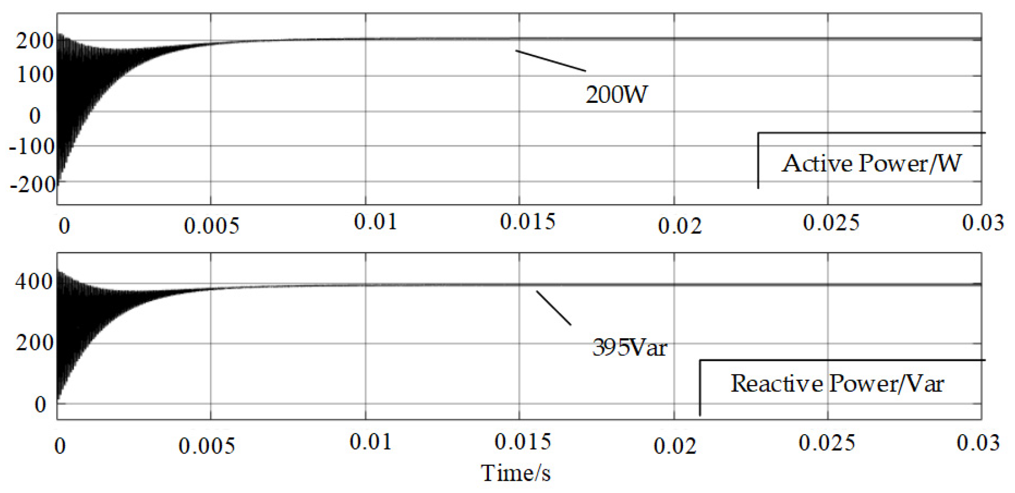
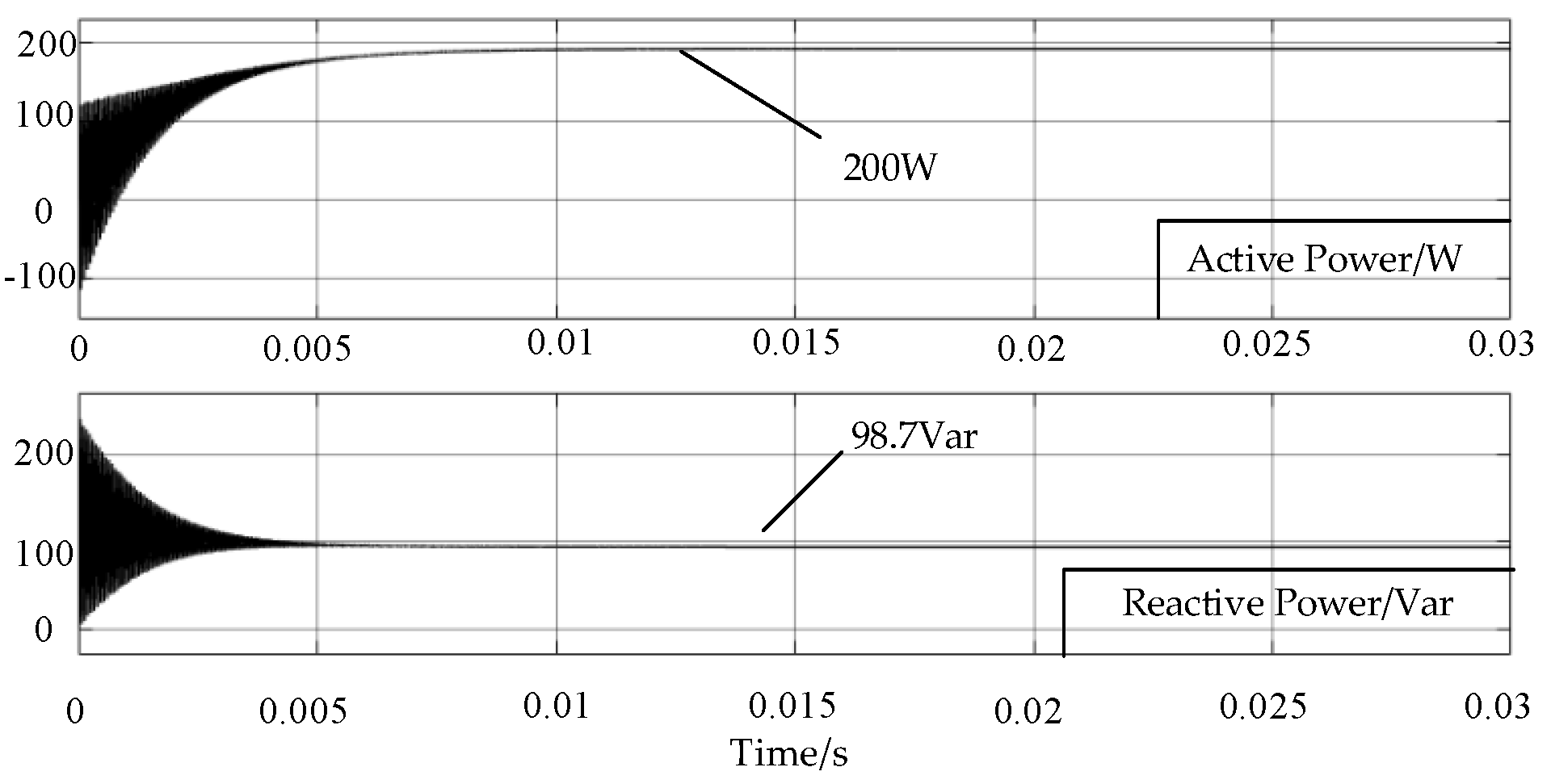
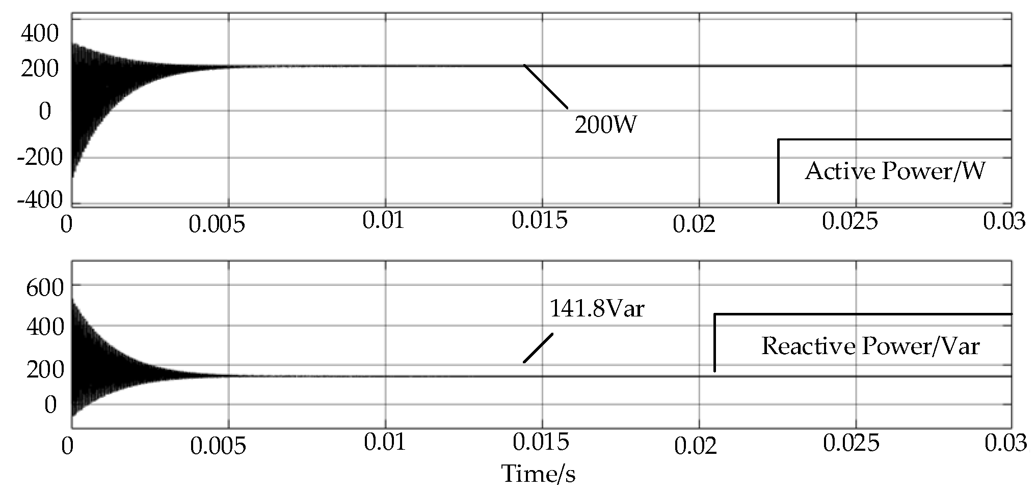
| Output Power | Phase-Shift Angle Combination | Reactive Power Value |
|---|---|---|
| 200 W | (57°, 213°) | 86.8 Var |
| (40°, 171°) | 109.5 Var | |
| (49°, 190°) | 103.2 Var |
Publisher’s Note: MDPI stays neutral with regard to jurisdictional claims in published maps and institutional affiliations. |
© 2022 by the authors. Licensee MDPI, Basel, Switzerland. This article is an open access article distributed under the terms and conditions of the Creative Commons Attribution (CC BY) license (https://creativecommons.org/licenses/by/4.0/).
Share and Cite
Wu, J.; Zhang, W.; Sun, X.; Su, X. Research on Reactive Power Optimization Control of a Series-Resonant Dual-Active-Bridge Converter. Energies 2022, 15, 3856. https://doi.org/10.3390/en15113856
Wu J, Zhang W, Sun X, Su X. Research on Reactive Power Optimization Control of a Series-Resonant Dual-Active-Bridge Converter. Energies. 2022; 15(11):3856. https://doi.org/10.3390/en15113856
Chicago/Turabian StyleWu, Junjuan, Wei Zhang, Xiaofeng Sun, and Xinyu Su. 2022. "Research on Reactive Power Optimization Control of a Series-Resonant Dual-Active-Bridge Converter" Energies 15, no. 11: 3856. https://doi.org/10.3390/en15113856
APA StyleWu, J., Zhang, W., Sun, X., & Su, X. (2022). Research on Reactive Power Optimization Control of a Series-Resonant Dual-Active-Bridge Converter. Energies, 15(11), 3856. https://doi.org/10.3390/en15113856