Article

Research on Reactive Power Optimization Control of a Series-Resonant Dual-Active-Bridge Converter

Key Lab of Power Electronics for Energy Conservation and Motor Drive of Hebei Province, Yanshan University, Qinhuangdao 066004, China
*
Author to whom correspondence should be addressed.
Energies 2022, 15(11), 3856; https://doi.org/10.3390/en15113856
Submission received: 18 April 2022 / Revised: 12 May 2022 / Accepted: 13 May 2022 / Published: 24 May 2022

Abstract

:
In order to meet the demands of the bidirectional transmission of electric vehicle charger power, a series-resonant dual-active-bridge (DAB) converter is investigated in this paper. Firstly, the active and reactive power and zero voltage switching (ZVS) conditions of the full-bridge arm under extended phase-shift modulation, dual phase-shift modulation and triple phase-shift modulation are analyzed. Secondly, with the minimum reactive power as the optimization objective, the extended phase shift (EPS) is finally selected as the modulation method after comparing the minimum reactive power under various modulation methods when the normalized value of active power is varied in the range of 0–1. By constructing the objective function and determining the constraints, an off-line reactive power–minimization control strategy is proposed to achieve the ZVS of the full-bridge arm and, finally, the feasibility of the proposed control strategy is verified by simulation and experiment.

1. Introduction

A dual-active-bridge (DAB) DC–DC converter [1] is widely used in electric vehicles, energy storage systems, microgrid and other fields because it can realize bidirectional power transmission. It has the advantages of high modularity, easy ZVS soft switching, electrical isolation of input and output and so on. In the wide gain range and wide load range, the traditional single phase shift (SPS) has only one inter bridge phase-shift angle, which reduces the soft-switching range of the switching tube of the DAB converter, and the problem of the return power of the DAB converter under this control is more serious [2]. Therefore, scholars generally expand the soft-switching range of the DAB converter through modulation strategies [3,4,5,6], such as extended phase shift (EPS), dual phase shift (DPS) and triple phase shift (TPS), so as to improve power transmission efficiency. In order to further improve the efficiency of DAB converters, various optimized phase-shift control strategies have been proposed one after another. The essence of these optimization algorithms is to make the DAB converter always work on the optimal control point, thus reducing losses and improving efficiency. For example, reference [7] proposed a PWM phase-shift control, which adds the duty cycle control of the output to the phase-shift control, where both the phase-shift angle and duty cycle are used to reduce the current stress. Among the various optimal control strategies, the current RMS-optimized control is the most common [8,9]. However, the derivation process of current RMS-optimized control is complex and requires a high precision current detection circuit. Therefore, in recent years, reactive power optimal control has attracted more and more attention. Reference [10] analyzed and optimized the return power of a DAB converter under EPS modulation, which can effectively improve the transmission efficiency. Reference [11] proposed an optimal control scheme based on TPS modulation. References [12,13] propose reactive power–optimized control, but these papers define the return power as reactive power. However, reactive power defined in this way exists only when the polarity of voltage and current are reversed. In reality, the presence of the inductor causes the converter to always absorb reactive power, regardless of the power transfer level, and reactive power values are always present and fluctuating. In reference [14], an optimal control strategy for a TPS-modulated DAB converter with reactive power expression as the objective function is proposed, which significantly improves the efficiency of the converter at light load and wide gain. Reference [15] searches for the minimum value of the rms value of the inductor current and finally derives the expressions between each phase-shift angle when the current rms value is minimum, but does not decouple the expressions from each other, so the relationship between the phase-shift angle and the transmitted power cannot be obtained quantitatively, and the control is not convenient.
In recent years, in order to improve the efficiency of DAB converters and improve the circuit power density, resonant the DAB converter has gradually become a research hotspot. Among them, the resonant dual-active-bridge converter composed of a DAB and an LC resonant tank only adds one resonant capacitance to the DAB topology. The DAB converter can be regarded as a limit case when the capacitance is infinite, so the series-resonant DAB converter has all the advantages of the DAB. Reference [16] points out that increasing the resonant capacitance can make the resonant current close to the sine wave and effectively filter out the DC current component of the transformer; moreover, it can reduce the eddy-current loss of transformer winding and help to reduce the off loss of the switch. However, the resonant DAB has the same problems as the traditional DAB. For example, the soft-switching range are reduced under light load, and when the voltages of the primary and secondary sides of the transformer do not match, the reactive power is large, which has a great impact on the efficiency of the converter.
This paper selects a series-resonant DAB converter as the research object and analyzes the relationship between the phase-shift modulation method and the minimum reactive power and soft switching of the full-bridge arm when the output power changes from no-load to full-load by comparing the active power and reactive power under three modulation methods of EPS, DPS and TPS so as to select an optimal modulation method for reactive power optimization, and give the specific optimization. The final combination of phase-shift angle for minimum reactive power is obtained to reduce the proportion of reactive power in the converter operation and thus improve the system efficiency.

2. Basic Characteristics of the Converter and Reactive Power Analysis

2.1. Introduction of Series-Resonant Dual-Active-Bridge Converter Topology

Figure 1 shows the circuit schematic diagram of the series-resonant DAB converter in which the input voltage Vin, the output voltage Vo, the resonant inductance Lr, the resonant capacitor Cr and the transformer on the original side turns a ratio of n = N1/N2. Enter the power and output power supply side in parallel one filter capacitor Cin and Co. Defining the voltage gain of the converter is M = nVo/Vin. The four bridge arms of the dual active bridge are represented by A, B, C and D, respectively.
In this paper, phase-shift modulation is adopted, the duty ratio of all switching tubes is 50% and the upper and lower tubes of the same bridge arm are complementary conductive. In phase-shift modulation, three control variables are involved: phase-shift angle φAD between bridges, phase-shift angles φAB within bridges and φDC. Define φAD as the phase-shift angle between S1 of bridge arm A and S7 of bridge arm D, and the range is −π < φAD < π; φAB is defined as the phase-shift angle between upper tube S1 of bridge arm A and upper tube S3 of bridge arm B, the range is 0 < φAB < 2π; φDC is defined as the phase-shift angle between upper tube S7 of bridge arm D and upper tube S5 of bridge arm C, and the range is 0 < φDC < 2π.
Because the harmonic content of resonant converter is low, this paper adopts fundamental wave analysis method to analyze and converts the secondary side of the transformer to the original side. The equivalent circuit is shown in Figure 2, where, u1 (t) is the fundamental component of uAB, u2 (t) is the fundamental component of n*uCD and iL is the fundamental component of resonant current. The resonant groove impedance is X = ω L r 1 ω C r .

2.2. Steady-State Mathematical Model under Three Modulation Strategies

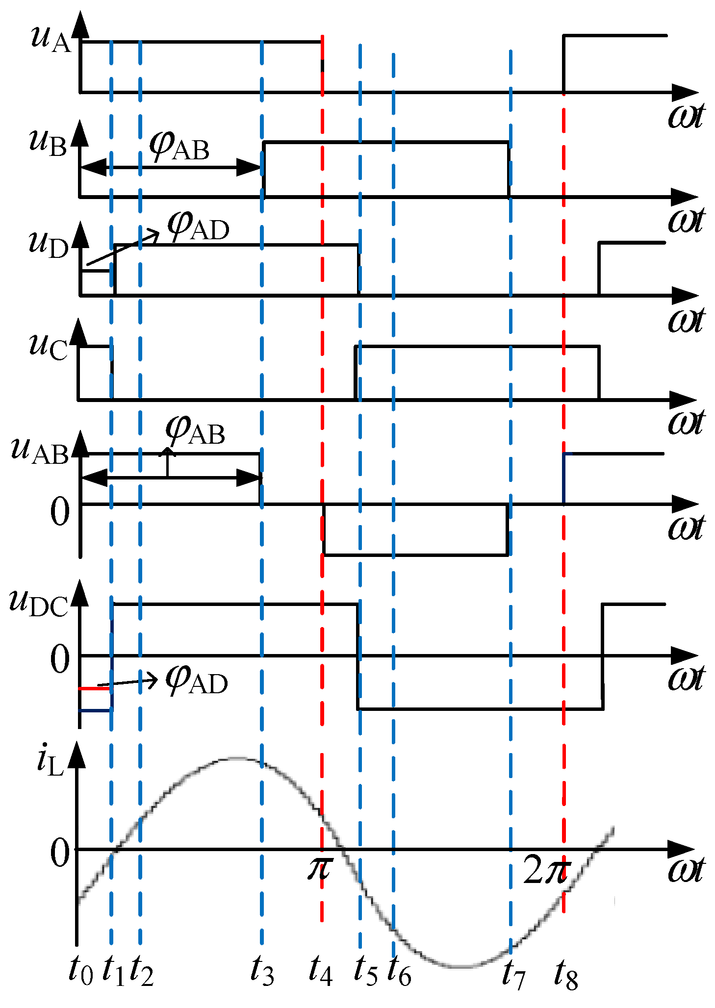
The working waveform of the series-resonant DAB converter in EPS modulation is shown in Figure 3, where uA, uB, uC and uD are the drive signals of the four bridge arms, uAB and uCD are the midpoint voltages of the arms of two active bridges and iL is current flowing through the inductance.
The converter has 8 operating modes per cycle under EPS phase-shift control, of which the operating modes from t0 to t4 are completely symmetrical with t5 to t8, and only the first four are analyzed.
(1)
t0t1 phase
The t0 moment is the initial moment, before this state, S2 and D4 are on, while the resonant current is negative, at the t0 moment, S2 is disconnected and the driving signal reaches S1; but since the current cannot be changed suddenly, the resonant slot current is still negative, so D1 and D4 are on. The secondary side of the transformer D5 and D8 are on, the voltage direction applied to both ends of the resonant slot is opposite to the current flow, resulting in the absolute value of current gradually decreasing, and when it decreases to 0, the energy is fed back from the resonant tank to the current side, and D1, D4, D5 and D8 are on in this stage.
(2)
t1t2 stage
At the moment of t1, the trigger pulse reaches S7, the current is naturally transferred to S7, S6 conduction, the primary state of the transformer remains unchanged, and the circulation path of the secondary side becomes S7, S6 This state continues until the voltage of the secondary side is reduced to the transformer induction voltage and this stage ends. In this stage, D1, D4, S7 and S6 are in the conduction state.
(3)
t2t3 phase
At the moment of t2, the absolute value of resonant current decreases to 0. S1 and S4 realize zero voltage switching; the resonant current is about to increase positively, and the transformer secondary current flow path becomes D7 and D6. S1, S4, D7 and D6 are on in this stage.
(4)
t3t4 phase
At moment t4, S4 is disconnected. At this time the inductor current is positive, causing the current path to switch from S4 to D3, with S1 and D3 on for the high-voltage side, and D5 and D8 on for the low-voltage side. At the same time, the resonant tank current starts to decrease gradually from the peak due to the voltage applied to both ends of the resonant tank and the opposite direction of the resonant current flow. In this stage S1, D7, D3 and D6 are on.
According to the steady-state working waveform combined with fundamental wave analysis, the time-domain expressions of the two fundamental wave voltages in Figure 2 are shown in Equations (1) and (2):
u 1 . EPS ( ω t ) = 4 V in π sin ( φ AB 2 ) sin ( ω t + π φ AB 2 )
u 2 . EPS ( ω t ) = 4 M V in π sin ( ω t φ AD )
In order to calculate the complex power using the phase volume method, the phase volumes of the fundamental voltages u1(ωt) and u2(ωt) are defined here as U ˙ 1 and U ˙ 2 , and the expressions for both are shown in Equations (3) and (4):
U 1 . EPS = 2 π [ ( 1 cos φ AB ) + j sin φ AB ]
U ˙ 2 . EPS = 2 2 M V in π [ cos ( φ AD ) j sin ( φ AD ) ]
The phasor of the fundamental wave component iL of resonant current is defined as I ˙ L , and its expression is shown in Equation (5):
I ˙ L = U ˙ 1 U ˙ 2 j X
According to Figure 2, the complex power transmitted by the AB bridge from the input side can be expressed as Equation (6):
S ˙ = U ˙ 1 × I ˙ L
By solving this, the active power and reactive power expressions of which can be obtained as Equations (7) and (8), respectively.
P EPS = 4 M V in 2 [ sin φ AD + sin ( φ AB φ AD ) ] π 2 X
Q EPS , pu = 4 M V in 2 π 2 X [ cos ( φ AB φ AD ) cos ( φ AD ) ] + 4 V in 2 π 2 X [ 1 cos ( φ AB ) ]
Taking P base = 8 M V in 2 / π 2 X as the power reference value, the expressions of the normalized value of active power PEPS,pu and reactive power QEPS,pu under EPS modulation are shown in Equations (9) and (10):
P EPS , pu = 0.5 sin φ AD + 0.5 sin ( φ AB φ AD )
Q EPS , pu = 0.5 cos ( φ AB φ AD ) 0.5 cos ( φ AD ) + 1 2 M [ 1 cos ( φ AB ) ]
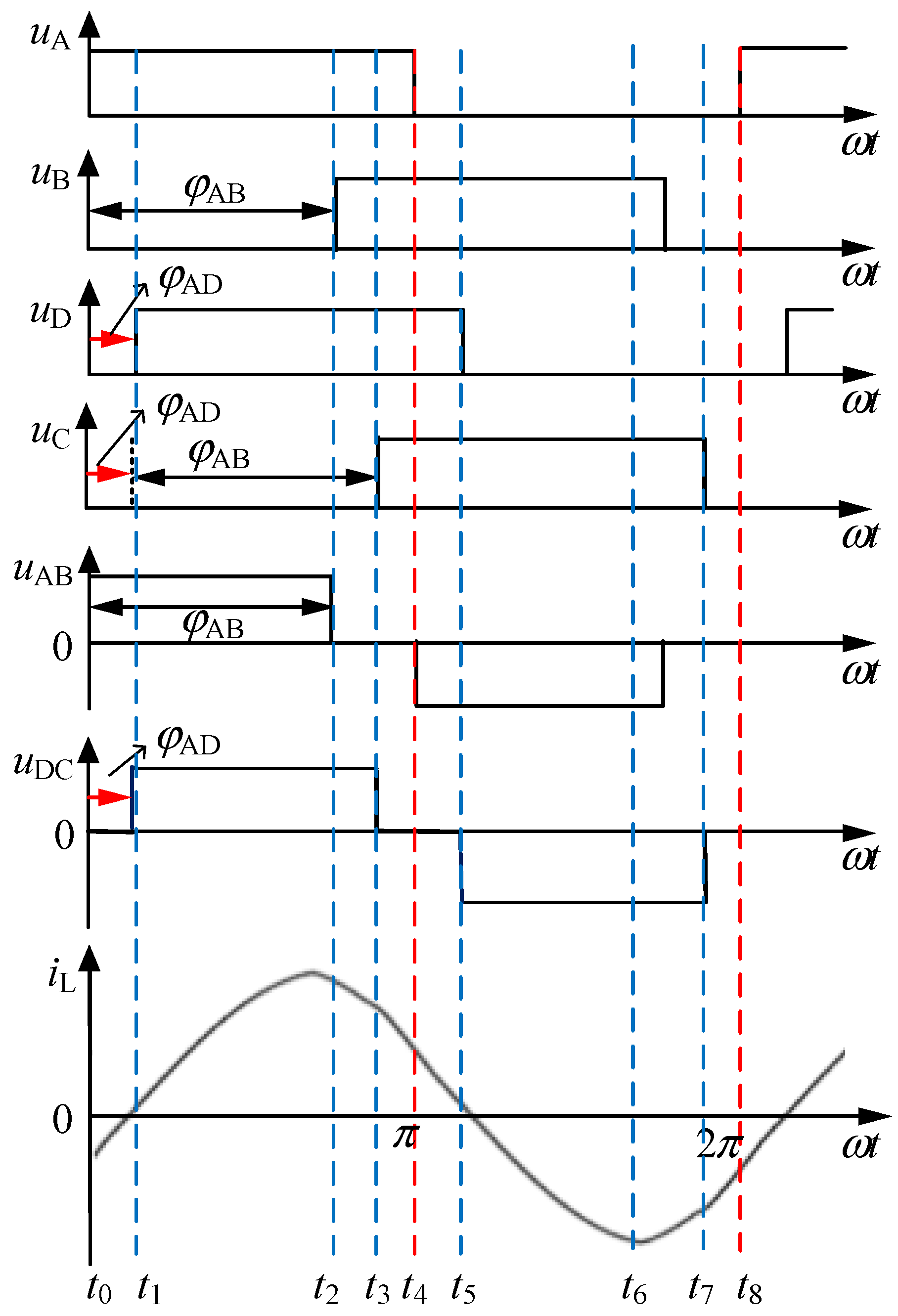
The working waveform of series-resonant DAB converter under DPS modulation is shown in Figure 4.
The converter operating modes are analyzed according to the steady-state operating waveform, which is divided into eight operating modes for each cycle under DPS modulation, of which the operating modes from t0 to t4 are completely symmetrical with t5 to t8.
(1)
Phase 1: t0t1
At the moment of t0, the converter transitions from mode 8 to mode 1, S1 and S4 are on, the inductor current is negative at this time, diodes D5 and D8 are on, and switching tube S1 achieves zero voltage turn-on. The transformer secondary side switching tubes S6 and S7 are in continuous conduction. Power flows from the inductor to the secondary side.
(2)
Phase 2: t1t2
Transformer primary side full-bridge switching tubes S1 and S4 continue to conduct, transformer secondary side switching tubes S6 and S7 conduct. t1 moment inductor current comes to over zero, and both sides of the transformer at the same time charge the inductor current.
(3)
Stage 3: t2t3
Transformer primary side full-bridge switching tube S2 is on, transformer secondary side switching tubes S6 and S7 are continuously on. The inductor current charges the primary side and the power flows from the inductor to the primary side.
(4)
Stage 4: t3t4
Transformer primary side full-bridge switching tube S2 is on, transformer secondary side switching tube S5 is on. The inductor current charges the secondary side.
Similarly, the time-domain expressions of the two fundamental voltages under DPS modulation can be derived as shown in Equations (11) and (12):
u 1 , DPS ( ω t ) = 4 V in π sin ( φ AB 2 ) sin ( ω t + π φ AB 2 )
u 2 , DPS ( ω t ) = 4 M V in π sin ( φ AB 2 ) × sin ( ω t φ AD + π φ AB 2 )
The same power reference values as for EPS modulation are chosen. The derived expressions for the normalized value of active power PDPS,pu and reactive power QDPS,pu under DPS modulation are given in (13) and (14) below:
P DPS , pu = 0.5 × ( 1 cos φ AB ) × sin φ AD
Q DPS , pu = 1 2 M ( 1 cos φ AB ) 0.5 × ( 1 cos φ AB ) × cos φ AD
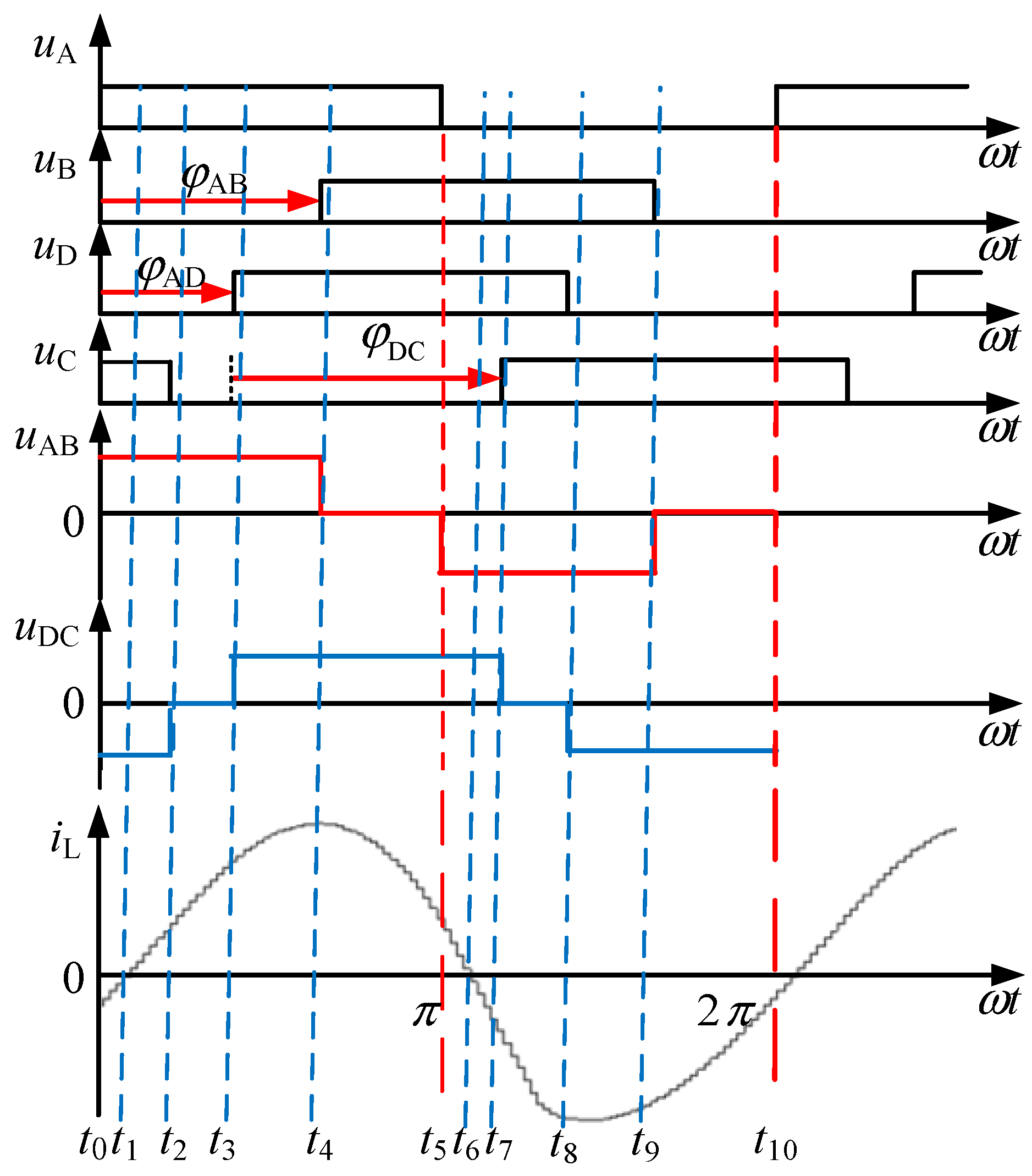
The working waveform of the series-resonant DAB converter under TPS modulation is shown in Figure 5.
The model is mainly divided into 10 working states, of which the first 1–5 working states and 6–10 working states are symmetrical, so only the first 5 working states are analyzed.
(1)
Phase 1: t0t1
At the moment of t0, the converter transitions from mode 10 to mode 1, S2 turns off, the inductor current is negative at this time, diode D1 conducts, and switching tube S1 achieves zero voltage turn-on. Switching tubes S6 and S7 on the secondary side of the transformer are continuously on. Power flows from the inductor to the secondary side.
(2)
Phase 2: t1t2
At moment t1, the primary side of the full-bridge switching tube S3 off, at this time the inductor current is negative, diode D4 is in natural conduction, switching tube S4 achieves zero-voltage opening, the transformer secondary side switching tubes S6 and S7 continue to conduct.
(3)
Phase 3: t2t3
Transformer primary side full-bridge switching tube S1, S4 continue to conduct, transformer secondary side switching tubes S6 and S7 continue to conduct. t2 moment inductor current comes to over the zero point and both sides of the transformer at the same time charge the inductor current.
(4)
Phase 4: t3t4
At moment t3, the secondary side switching tube S6 off, S5 voltage discharge at both ends to 0, diode D5 natural conduction, switching tube S5 to achieve zero voltage open, the transformer primary side switching tube S1, S4 continue to conduct, to charge the inductor.
(5)
Phase V: t4t5
At moment t4, the secondary side of the full-bridge switching tube S7 off, the voltage at both ends of S8 discharge to 0, diode D8 natural conduction, switching tube S8 to achieve zero voltage open, the transformer primary side S1, S4 continue to conduct.
Similarly, the time domain expressions of the two fundamental wave voltages under TPS modulation can be derived (15) and (16) shown:
u 1 , TPS ( ω t ) = 4 V in π sin ( φ AB 2 ) sin ( ω t + π φ AB 2 )
u 2 , TPS ( ω t ) = 4 M V in π sin ( φ DC 2 ) × sin ( ω t φ AD + π φ DC 2 )
The same power reference values as for EPS modulation are chosen. The expressions for the normalized value of active power PTPS,pu and reactive power QTPS,pu under TPS modulation are derived as follows (17) and (18).
P TPS , pu = 0 . 25 × [ sin ( φ AD + φ CD φ AB ) + sin φ AD + sin ( φ AB φ AD ) sin ( φ AD + φ CD )
Q TPS , pu = 0.25 [ cos ( φ AD + φ CD φ AB ) cos φ AD + cos ( φ AB φ AD ) + cos ( φ AD + φ DC ) + 1 2 M ( 1 cos φ AB )

2.3. Analysis of Soft-Switching Characteristics under Three Modulation Strategies

In order to realize zero voltage switching (ZVS) of all switches, the anti-parallel diode of each switch needs to be turned on before the switch itself. Therefore, according to the positive current direction shown in Figure 1, it can be seen that in order to realize ZVS, a bridge arm needs to ensure that the inductive current iL < 0 at the moment when the upper tube S1 is turned on; to realize ZVS for bridge arm B, it is necessary to ensure that the inductor current iL > 0 at the moment when the upper tube S3 is turned on. To realize ZVS for D bridge arm, it is necessary to ensure that the inductance current iL > 0 at the moment when the upper tube S7 is turned on; to realize ZVS for bridge arm C, it is necessary to ensure that the inductor current iL < 0 at the moment when the upper tube S5 is turned on.
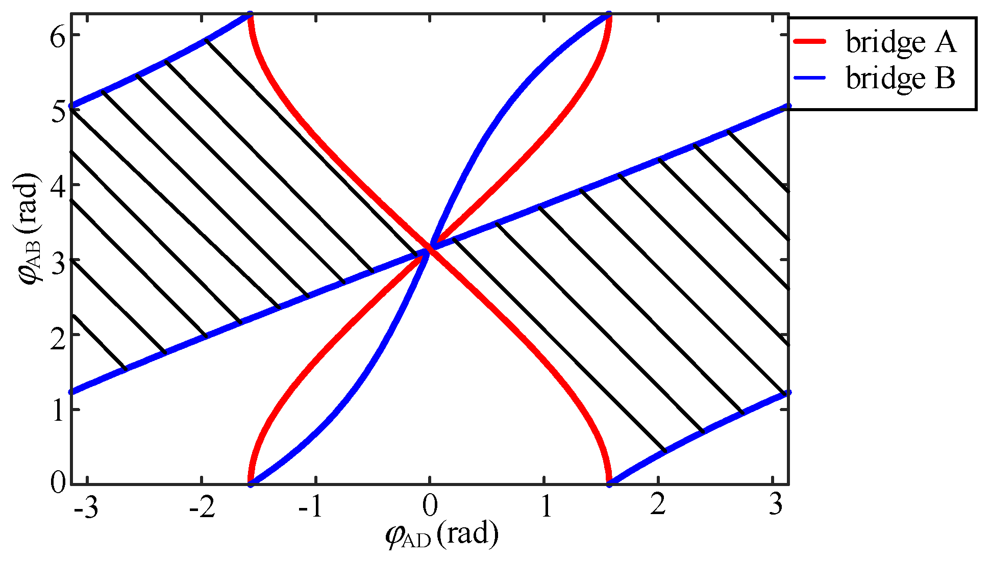
According to Figure 3, the conditions for realizing full-bridge arm ZVS under EPS modulation mode can be obtained, as shown in Equation (19). The full-bridge arm ZVS area drawn by Matlab is shown in Figure 6. The curves of various colors in the figure are the boundary lines of each bridge arm to realize ZVS.
{ sin 2 ( φ AB 2 ) + M cos ( φ AD ) < 0   A   bridge   leg sin 2 ( φ AB 2 ) + M cos ( φ AB φ AD ) > 0   B   bridge   leg sin ( φ AB 2 ) × sin ( φ AD φ AB 2 ) + M > 0   C , D   bridge   leg
According to Figure 4, the conditions for realizing ZVS of full-bridge arm in DPS modulation mode can be obtained, as shown in Equation (20):
{ sin 2 ( φ AB 2 ) + M sin ( φ AB 2 ) sin ( ϕ AB / 2 + ϕ AD ) < 0   A   bridge   leg sin 2 ( φ AB 2 ) M sin ( φ AB 2 ) sin ( φ AB 2 φ AD ) > 0   B   bridge   leg sin ( φ AB 2 ) sin ( φ AD φ AB 2 ) + M sin 2 ( φ AB 2 ) > 0   C   bridge   leg sin ( φ AB 2 ) sin ( φ AD + φ AB 2 ) M sin 2 ( φ AB 2 ) < 0   D   bridge   leg
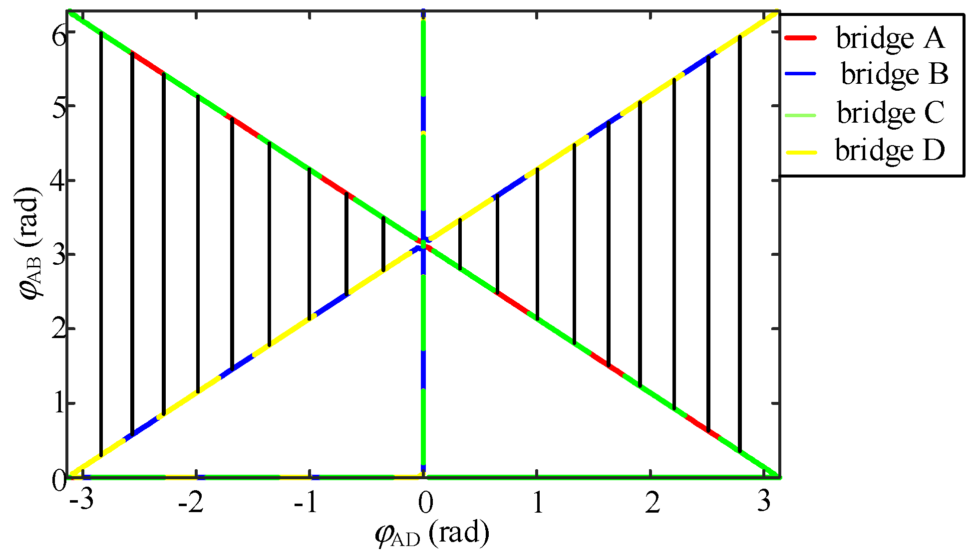
The full-bridge arm ZVS area drawn by MATLAB is shown in Figure 7.
According to Figure 5, the conditions for realizing ZVS of the full-bridge arm in TPS modulation mode can be obtained, as shown in Equation (21):
{ sin 2 ( ϕ AB 2 ) + sin ( ϕ DC 2 ) sin ( ϕ AD + ϕ DC 2 ) < 0   A   bridge   leg sin 2 ( ϕ AB 2 ) + sin ( ϕ DC 2 ) sin ( ϕ DC 2 + ϕ AD ϕ AB ) > 0   B   bridge   leg sin ( ϕ AB 2 ) sin ( ϕ AD ϕ AB 2 ) + sin 2 ( ϕ DC 2 ) > 0   C   bridge   leg sin ( ϕ AB 2 ) sin ( ϕ AD + ϕ DC ϕ AB 2 ) sin 2 ( ϕ DC 2 ) < 0   D   bridge   leg
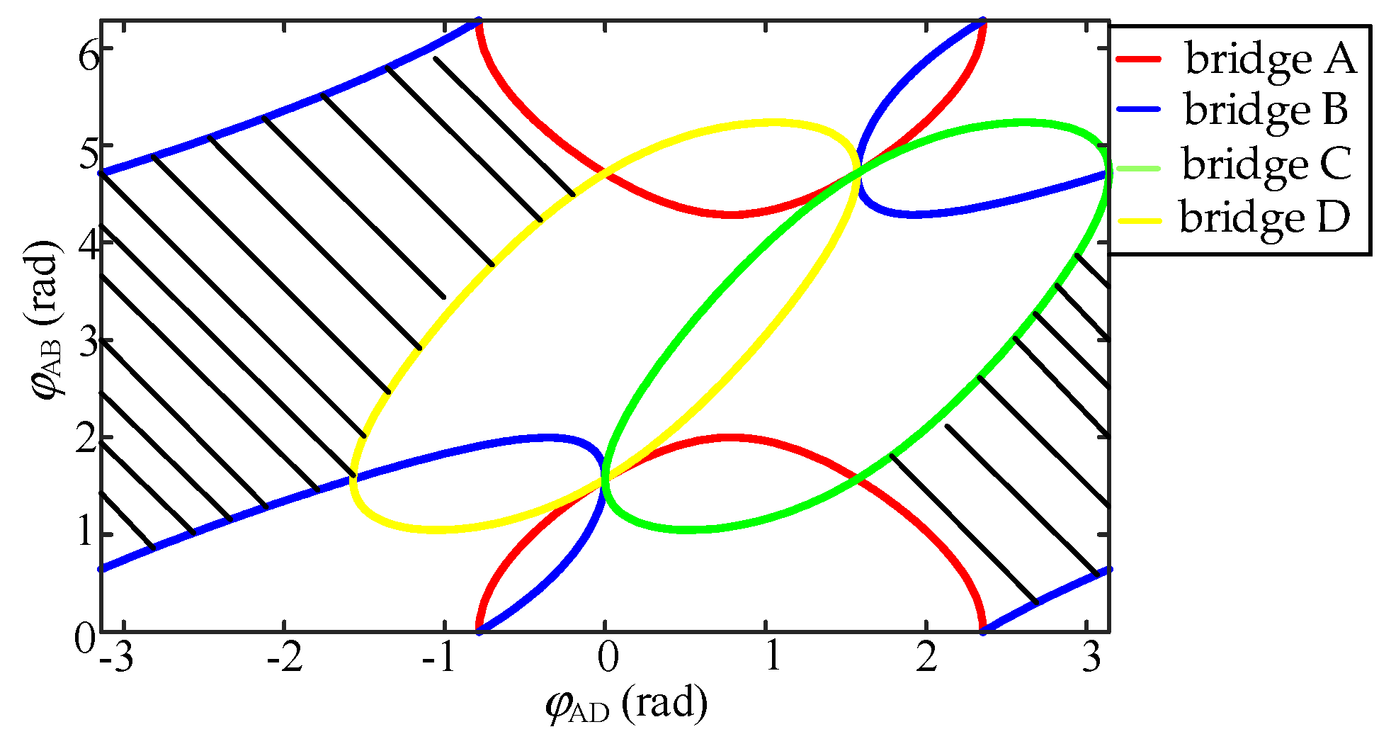
Since TPS contains three control quantities, in order to display the soft-switching area in the two-dimensional coordinate system, it is taken here that φDC = 90° for simulation. The ZVS area of the full-bridge arm drawn by Matlab is shown in Figure 8.
By comparing Figure 6 and Figure 7, it is not difficult to find that EPS modulation and DPS modulation have similar sizes in the soft-switching region of the full-bridge arm, while TPS modulation (φDC = 90°) has a smaller soft-switching region.

2.4. Minimum Reactive Power Analysis under Different Modulation Strategies

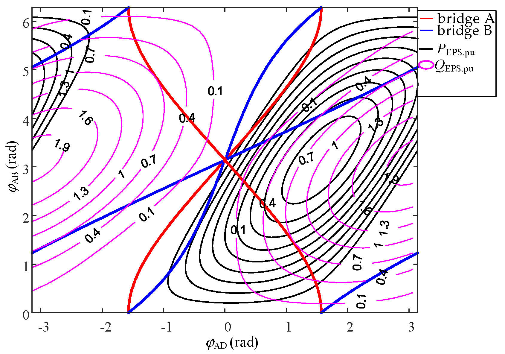
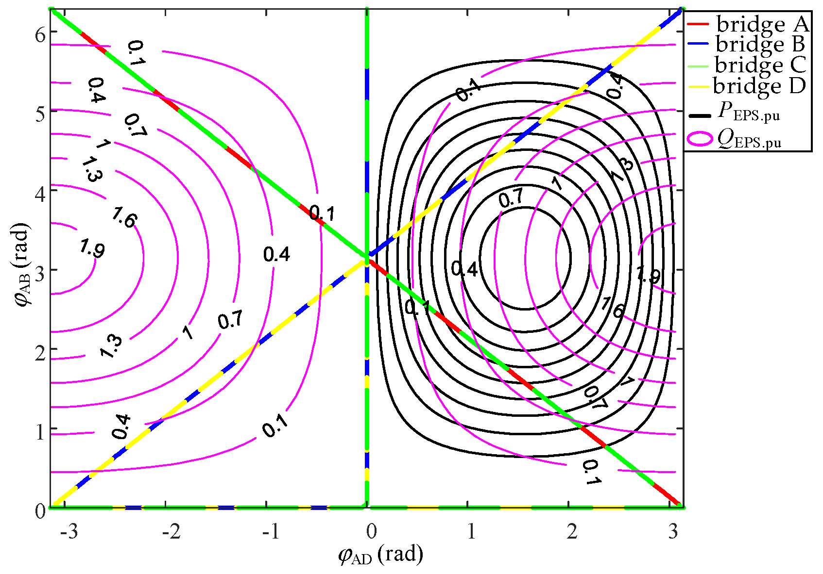
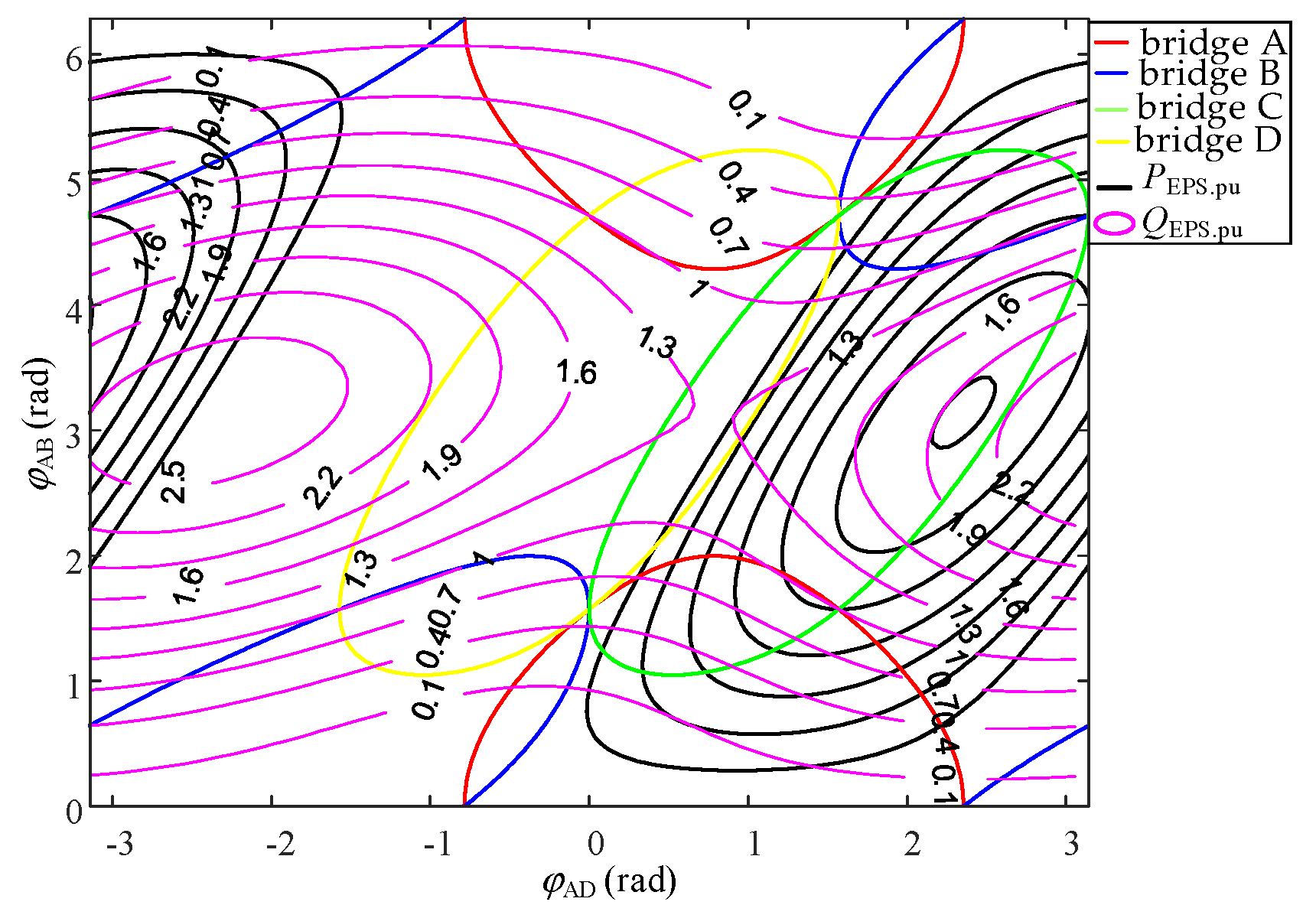
In order to analyze the minimum reactive power corresponding to the full-bridge ZVS under different modulation strategies, the unit value of active power is taken every 0.1 in the range of 0–1. Draw the full-bridge ZVS boundary line, the active power unit value curve and the reactive power contour line under the three modulation strategies in the same plane and, finally, obtain Figure 9, Figure 10 and Figure 11. The normalized value of the active power curve in the figure corresponds to a closed ellipse or oblique ellipse. Compare the minimum reactive power value of different modulation strategies when the gain M = 1. Through the reading of the data in Figure 9 and Figure 10, the minimum reactive value intersected by the unit value of different active power can be obtained. Under TPS modulation, the internal phase-shift angle of the secondary side bridge is given as φDC = 90°, the area where all active power curves are located is the hard-switching area.
According to the soft-switching boundary lines, the normalized value of the active power curves and the reactive power contours of the above three modulation modes, the EPS modulation mode achieves the largest area of full-bridge ZVS and the smallest reactive power value among the three modulation modes. TPS modulation reduces the range of the active power that can be transmitted due to the introduction of too many phase-shift angles and when PEPS.pu = 0.7, all are located in the hard-switching area. The minimum reactive power values at different active power unit values for different modulation modes are shown in Table 1.

3. Optimal Reactive Power Control Strategy

3.1. Series-Resonant DAB Reactive Power Optimization Control Strategy

Determine the objective function studied in this paper as in Equation (22):
Min [ Q EPS ( φ AD , φ AB ) ]
When the system transmits a certain value of active power, the active power trajectory is used as the limiting condition of the equation. As in Equation (23):
P o . pu = P EPS . pu ( φ AD , φ AB )
When the system transmits a certain value of active power, the active power value is taken as a known quantity, and the active power trajectory is taken as the limit condition of the equation, the functional expressions of the intra-bridge phase-shift angle φAB and the inter-bridge phase-shift angle φAD can be obtained, as in Equation (24):
φ AB = f ( φ AD , P EPS . pu )
Using 8MVin22X as the power reference value, the expression obtained is as in Equation (25):
P EPS . pu = 0.5 [ sin φ AD + sin ( φ AB φ AD ) ]
Two expressions for the phase-shift angle φAB within the bridge can be obtained as in Equations (26) and (27):
φ AB 1 = arcsin ( 2 P EPS . pu sin φ AD ) + φ AD
φ AB 2 = π + φ AD arcsin ( 2 P EPS . pu sin φ AD )
The two expressions of the intra-bridge phase-shift angle φAB are substituted into the expression of the reactive power standardized value, and the expression of the reactive power relative to the inter-bridge phase-shift angle φAD is obtained as in Equations (28) and (29):
Q EPS . pu 1 = 0.5 cos [ arcsin ( 2 P EPS . pu sin φ AD ) ] 0.5 cos φ AD + 1 2 M { 1 cos [ arcsin ( 2 P EPS . pu sin φ AD ) + φ AD ] }
Q EPS . pu 2 = 0.5 cos [ π arcsin ( 2 P EPS . pu sin φ AD ) ] 0.5 cos φ AD + 1 2 M { 1 cos [ π + φ AD arcsin ( 2 P EPS . pu sin φ AD ) ] }
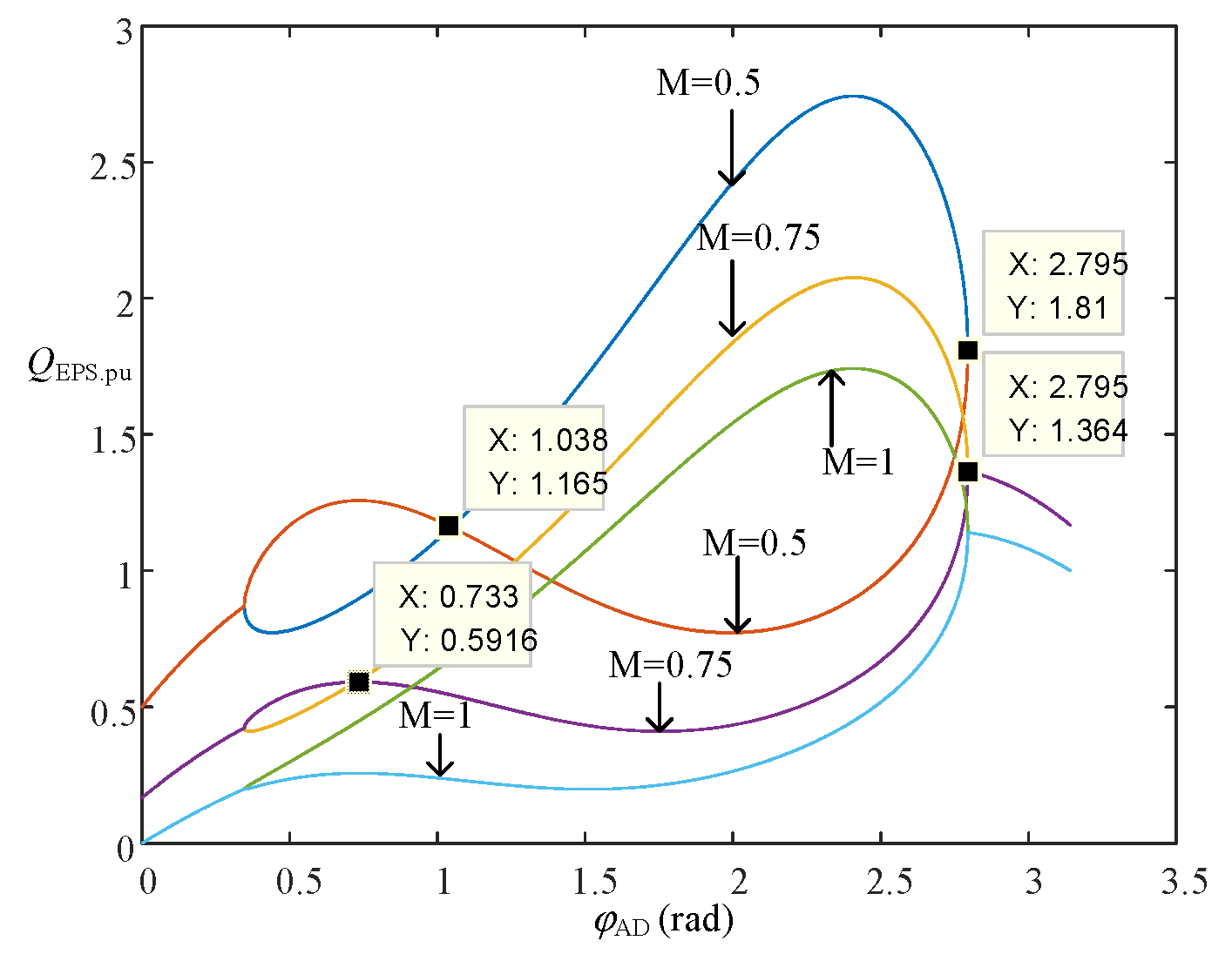
The three curves above in Figure 12 are the images of QEPS.pu1, and the three curves below are the images of QEPS.pu2. From the above relationship between the reactive power standardized value QEPS.pu and the inter-bridge phase-shift angle φAD under different gain M, it can be seen that when the gain M = 1, the image of QEPS.pu2 is always located below the image of QEPS.pu1, indicating that the same inter-bridge phase shift The reactive power value of QEPS.pu2 is always smaller than that of QEPS.pu1 when the phase angle shifts phase angle, and when the gain M is 0.5, the image of QEPS.pu2 is located above the image of QEPS.pu1 in the 0.33–1.03 radian range, so the reactive power value of QEPS.pu2 is larger than that of QEPS.pu1 in this range, and when M = 0.75, the reactive power value of QEPS.pu1 in the reactive power value of QEPS.pu2 is greater than that of QEPS.pu1 in this range; when M = 0.75, in the range of 0.35–0.73 radians, the image of QEPS.pu2 is located above the image of QEPS.pu1, and the reactive power value of QEPS.pu2 is greater than that of QEPS.pu1 in this range. The smaller the gain M, the larger the range of QEPS.pu2, but from the size of the range of the two, the QEPS.pu2 reactive power standardized value is always smaller than the larger range, and when the gain M = 1, the full range of the QEPS.pu2 value is constantly smaller than QEPS.pu1.
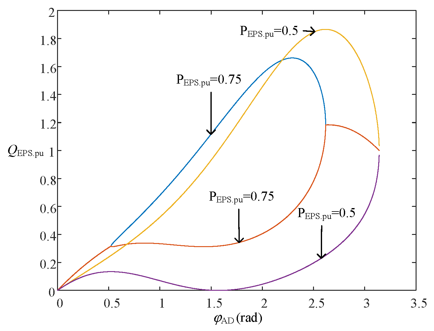
Keep the gain M = 1 constant, change the active power standardized value, the reactive power standardized value QEPS.pu, and the relationship between the inter-bridge phase-shift angle φAD is shown in Figure 13.
The top two curves in Figure 13 are images of QEPS.pu1 and the bottom two curves are images of QEPS.pu2. From Figure 13, it can be seen that changing the magnitude of the active power minimum value QEPS.pu does not affect the trend of the curve of the gain reactive power minimum value QEPS.pu and the inter-bridge phase-shift angle φAD, and the value of QEPS.pu1 is always larger than the value of QEPS.pu2 during the change of the inter-bridge phase-shift angle φAD. As the inter-bridge phase-shift angle φAD increases, the reactive power minimum value QEPS.pu is always increasing.
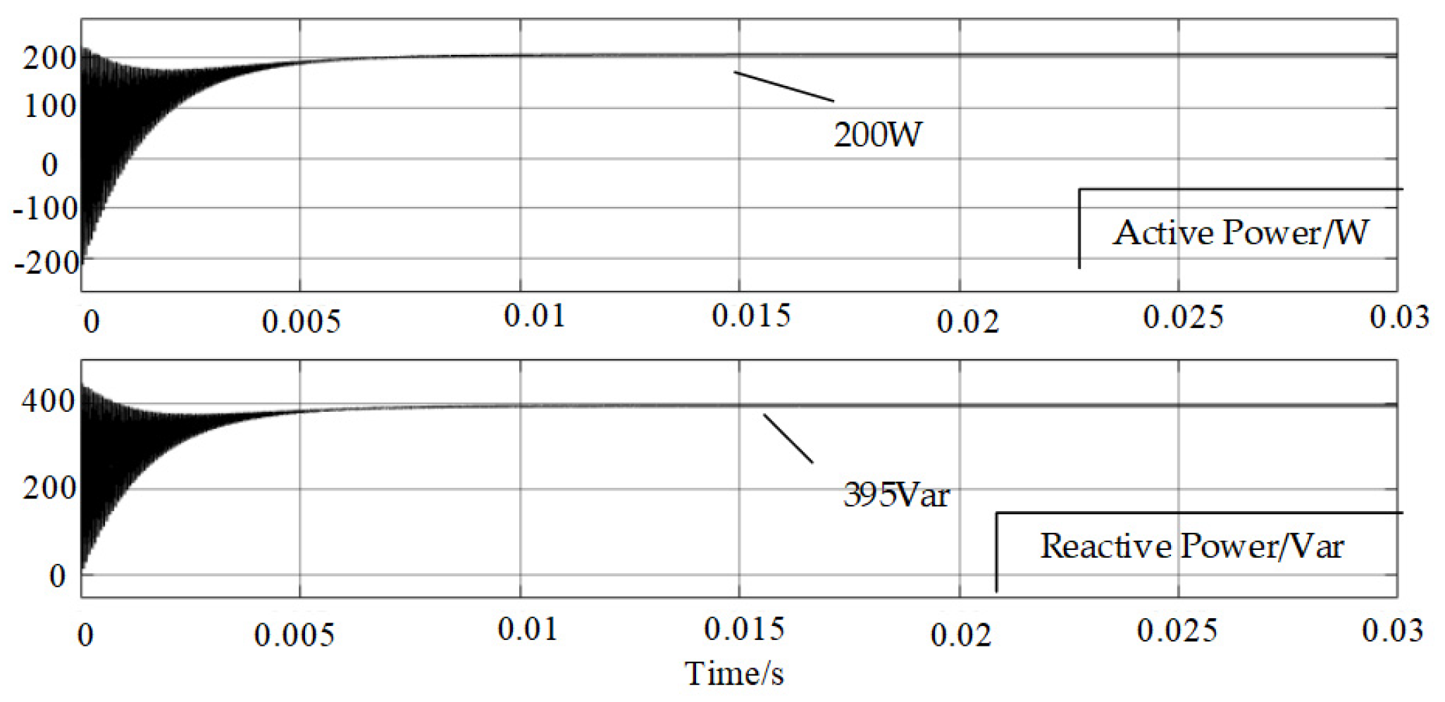
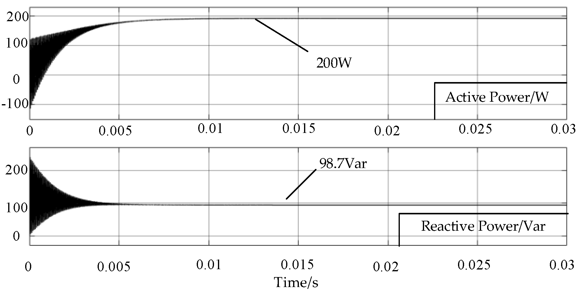
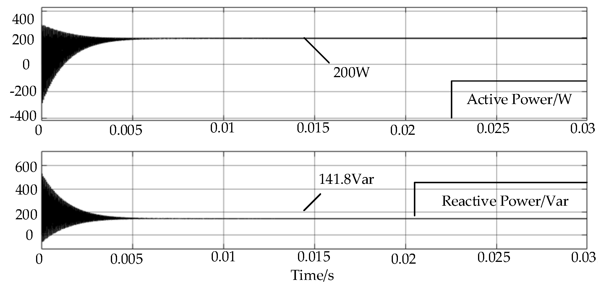
In order to prove the reliability of the formula, this paper verifies the formula by building a simulation through matlab, given the input voltage Vin = 100 V, output voltage Vo = 100 V and active power P = 200 W and finally verifies the reactive power data of equation QEPS.pu1 and equation QEPS.pu2 under different phase-shift angles when the gain M = 1, as shown in Table 2.
From the simulation results in Table 2 for different inter-bridge phase-shift angles, it can be seen that the reactive power value of equation QEPS.pu1 is always greater than that of equation QEPS.pu2. The simulation waveforms are given here for the inter-bridge phase-shift angle φAD = 30°, intra-bridge phase-shift angle φAB1 = 76.9° and φAB2 = 163.1°; inter-bridge phase-shift angle φAD = 90°, intra-bridge phase-shift angle φAB1 = 103° and φAB2 = 257°; and the simulation waveforms are shown in Figure 14, Figure 15, Figure 16 and Figure 17.
Since there is a certain error between the theoretical calculation and the simulation value, the active power values in the above simulation results are slightly smaller than the theoretical values, but they are within the error range. According to the comparison between the above analysis and the simulation results, it can be seen that when the gain M = 1, among the two inter-bridge phase-shift angles corresponding to the same inter-bridge phase-shift angle φAD, the one with the larger inter-bridge phase-shift angle value has a smaller reactive power value. When the gain M is less than 1, the small region Qepspu1 is smaller than Qepspu2; therefore, this paper selects the reactive power needed to make a judgment about the gain M, and then compares the size of the reactive power values of Equations (28) and (29).
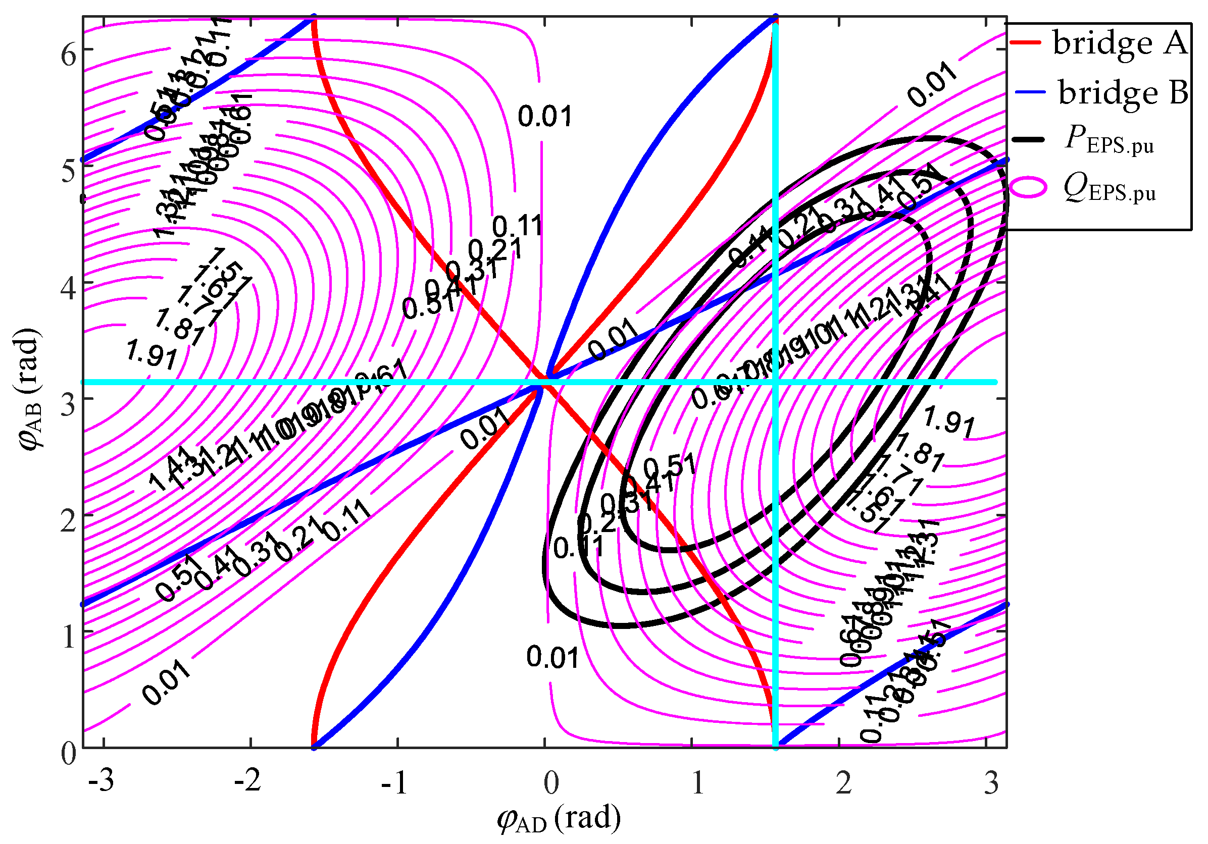
In the current power reference value, gain M = 1 for active power of 200 W and the corresponding active power standardized value is 0.62, so the intersection of the reactive power contour occurs when the normalized value of active power is 0.52, 0.62 and 0.72, respectively, is drawn as shown in Figure 18: the blue horizontal and vertical lines in the figure are the intra-bridge phase-shift angle φAB = π and the inter-bridge phase-shift angle φAD = π/2.
The following conclusions can be drawn from Figure 18:
(1)
In a certain active power standardized value, when the same inter-bridge phase-shift angle φAD corresponds to two intra-bridge phase-shift angles φAB and the larger the intra-bridge phase-shift angle, the smaller the value of the reactive power contour is handed over. Similarly, the same intra-bridge phase-shift angle φAB corresponds to two intra-bridge phase-shift angles φAD and the smaller value of the reactive power contour;
(2)
At a certain active value in the intersection with the reactive power contour, the closer to the right side of the image, the greater the value of the reactive power; the closer to the left side of the image, the smaller the value of the reactive power;
(3)
The minimum reactive power is located in the vicinity of the intra-bridge phase-shift angle φAB = π, which is near the single phase-shift modulation strategy.
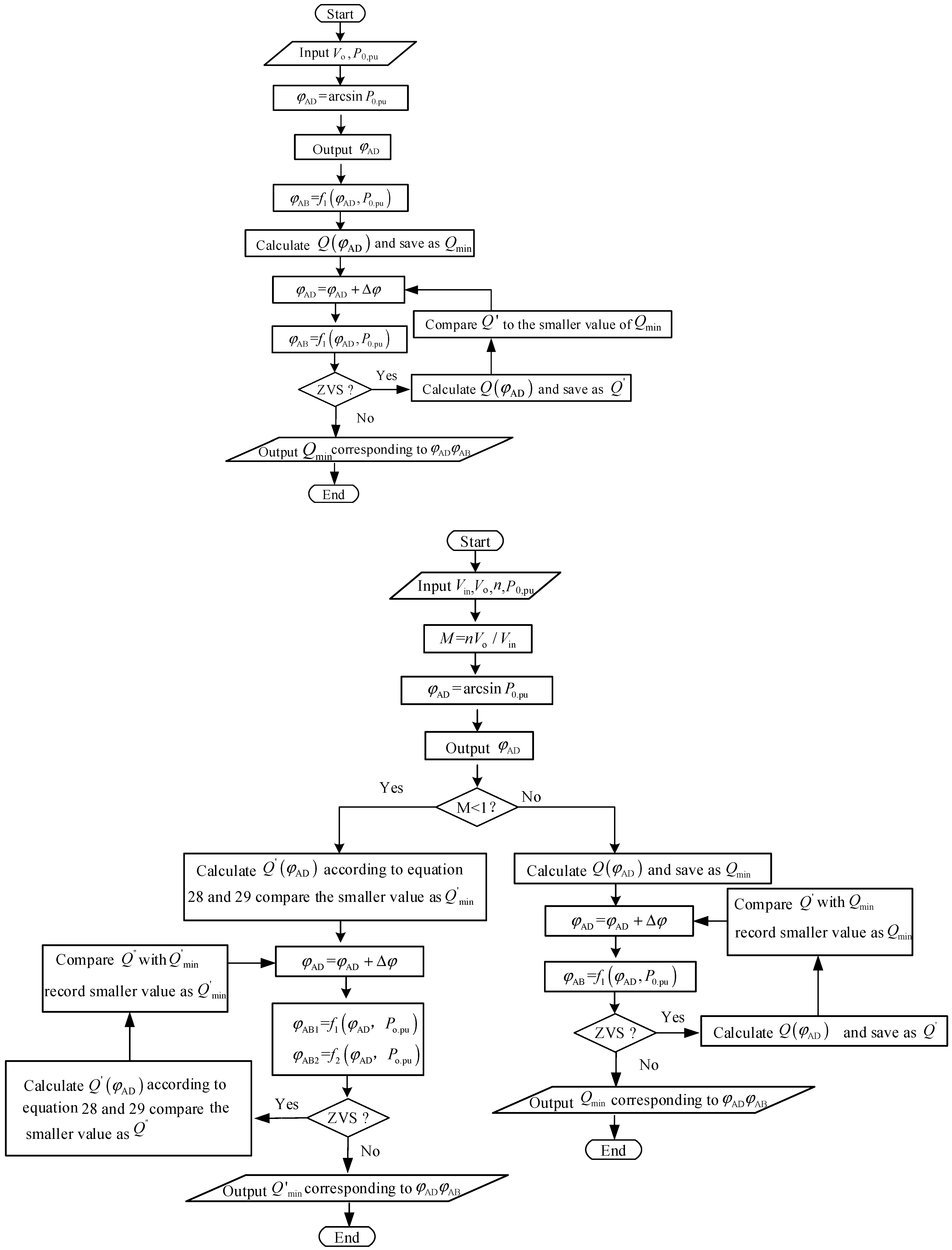
According to the above analysis, a reactive power minimization control measurement is designed in this paper. When the output voltage and active power standard minimum values are given, the system automatically performs the optimization search and finally outputs a combination of phase-shift angles with the minimum reactive power under the condition of realizing the full-bridge arm ZVS so that the reactive power accounts for the minimum in the system and thus improves the efficiency of the system.
As can be seen from Figure 18, the obtained minimum reactive power value under the full-bridge arm of ZVS is located near the intra-bridge phase-shift angle φAB = π, and the difference between the minimum reactive power value under the full-bridge arm of ZVS is very small in its upper and lower seeking directions, so only the upper direction of seeking is performed in this paper, which is based on the obtained single phase-shift angle φAD plus delta phi. The experiments and simulations that follow compare the reactive power minima in the upper and lower directions to express the small differences between them. The flow chart of the reactive power minimization control strategy designed in this paper is shown in Figure 19 below.
First, in the optimal reactive power control, input voltage, output voltage, transformer ratio and the normalized values of active power are first given to calculate the gain M. According to the active power expression of the single phase-shift control strategy, the inter-bridge phase-shift angle φAD can be found since the same active power output results in two inter-bridge phase-shift angles. According to the previous analysis, the smaller the inter-bridge phase-shift angle φAD is, the smaller the corresponding reactive power value is. Due to the optimization procedure, the system output inverse delta function results in the interval [0–π/2]. Make a determination of M. If M is not less than 1, substitute φAD into Formula (29), record the reactive power value as Qmin at this time, and then carry out the optimization solution cycle. Add a set step ∆φ to φAD, where the step ∆φ is given as 0.001 in the program, record it as φAD in the program, bring it into Formula (27) to get the corresponding intra-bridge phase-shift angle φAB, bring (φAD, φAB) into the full-bridge arm ZVS inequality to see if it satisfies the full-bridge arm ZVS inequality, and if it does, then bring (φAD, φAB) into Formula (29) and record the obtained Q(φAD) as Q’ and compare it with Qmin, record the smaller one as Qmin, record the phase-shift angle at this time as φAD, then go back to φAD and add a set step ∆φ, and so on until the obtained phase-shift angle does not meet the full-bridge arm ZVS output minimum reactive power value Qmin corresponding to the system, and give the number of times to seek and the corresponding best phase-shift angle combination according to the output requirements of the flow chart, and then look up in the table to get the best phase-shift angle combination corresponding to the minimum reactive power. If M is less than 1, put φAD into band Formulas (28) and (29), respectively, to get the corresponding Q’(AD), and record the smaller value as Qmin; then carry out another optimization solution cycle, add a set step to φAD similarly, ∆φ, according to Formulas (26) and (27), to obtain the corresponding intra-bridge phase-shift angle φAB, Substitute (φAD, φAB) into the ZVS inequality of full-bridge arm, compare the minimum value of reactive power obtained by the two sets of phase-shift angles and remember the smaller value as Q’’, compare it with Qmin and remember the smaller value as Qmin. This cycle is carried out until the obtained phase-shift angle does not meet ZVS and the minimum reactive power value Qmin corresponding to the system is output. According to the output requirements of the flow chart, the times and the corresponding optimal phase-shift angle combinations are given, and then the optimal phase-shift angle combination corresponding to the minimum reactive power is obtained by searching in the table.

3.2. Minimum Reactive Power Simulation Verification

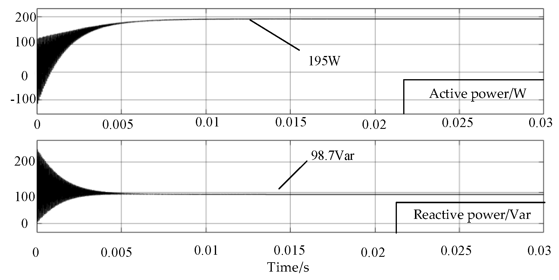
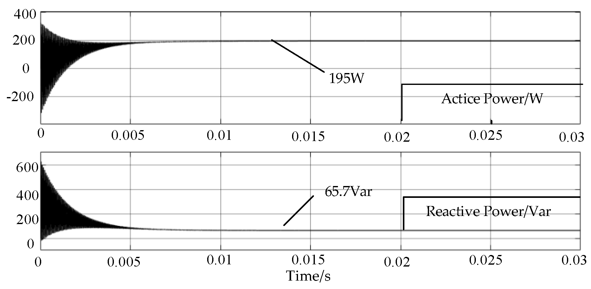
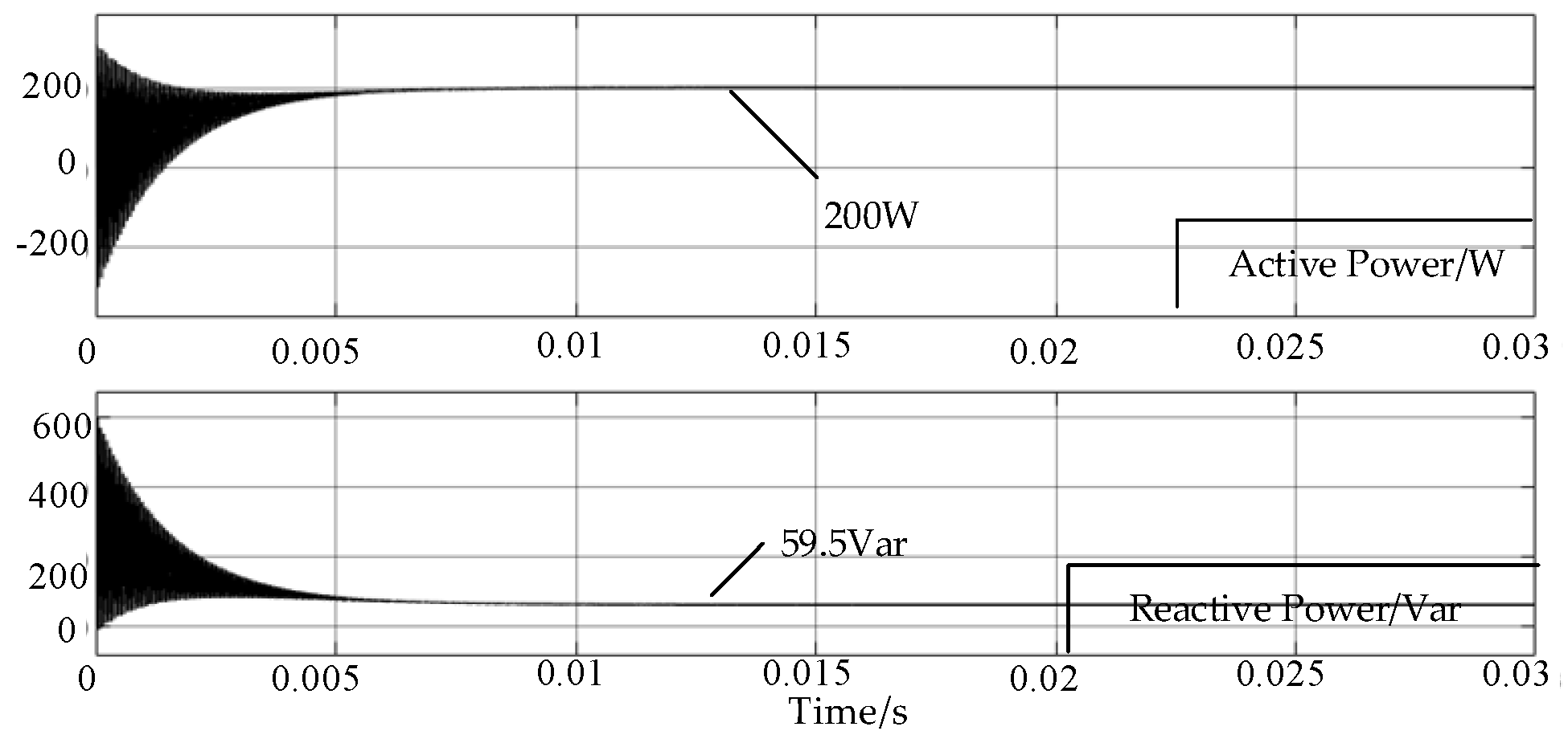
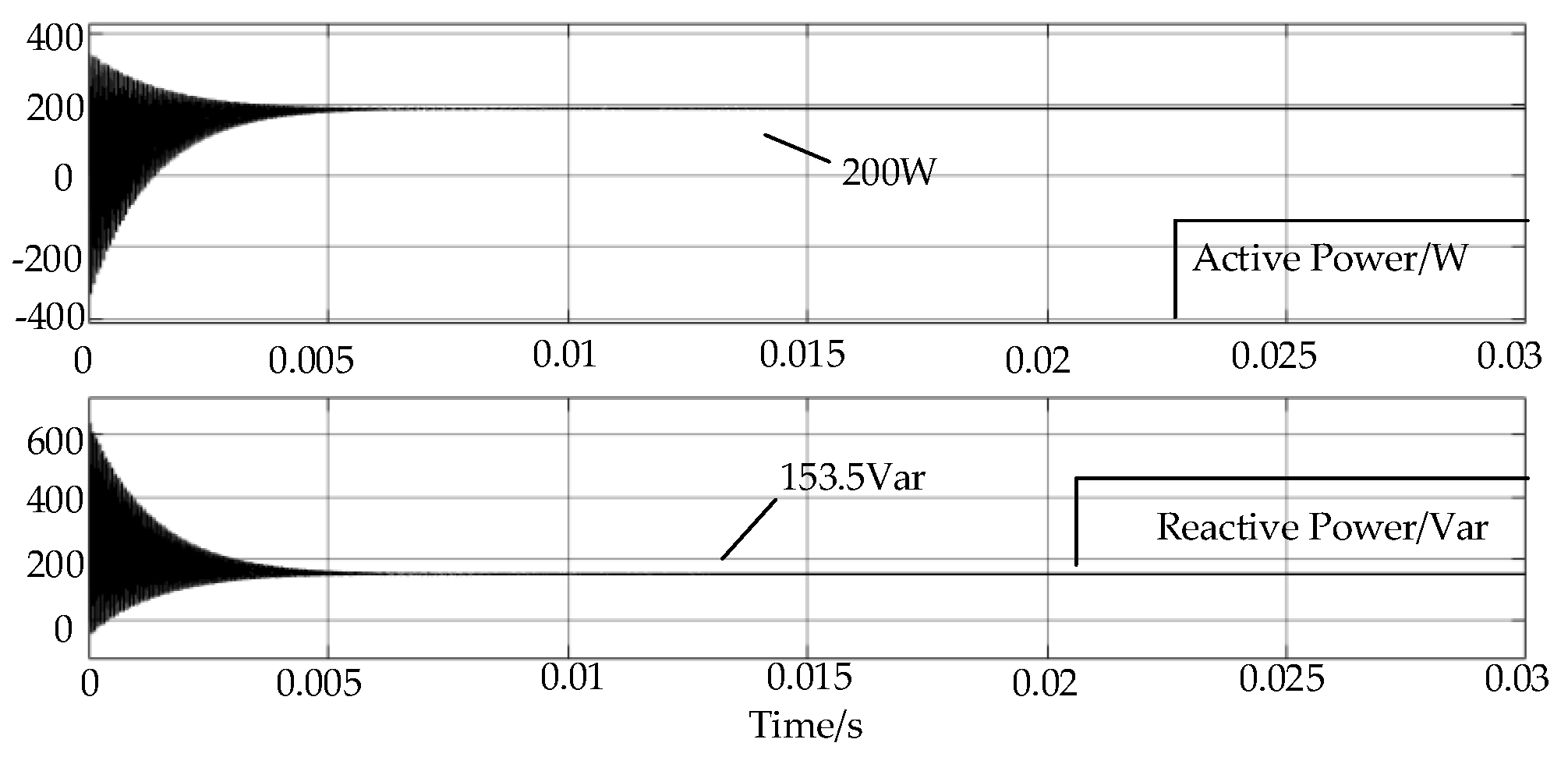
According to the control strategy proposed in this paper, the simulation was built in MATLAB for the experiment, and the reactive power value was compared by comparing the obtained phase-shift angle combination with other randomly selected points of the phase-shift angle combination. When the gain M = 1, according to the obtained phase-shift angle combination brought into the simulation with the phase-shift angle combination of (25.8°, 152°), the obtained the active and reactive power simulations are as shown in Figure 20.
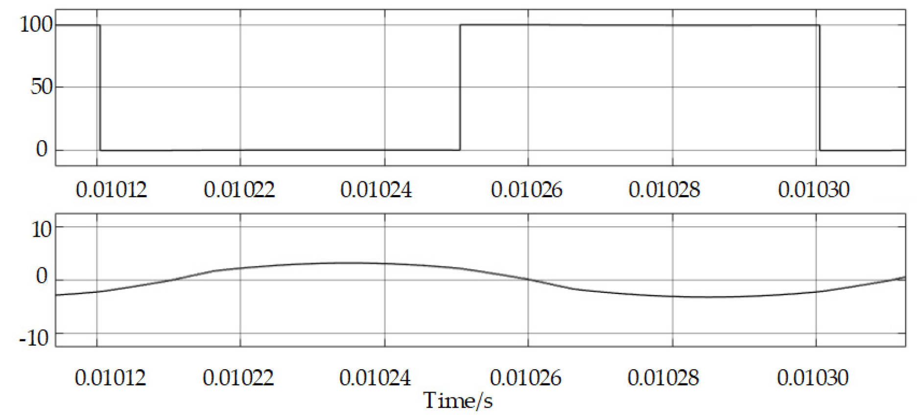
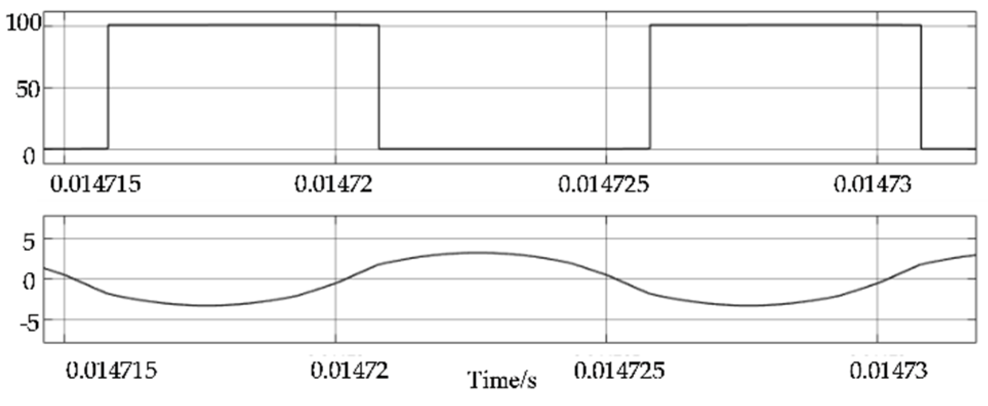
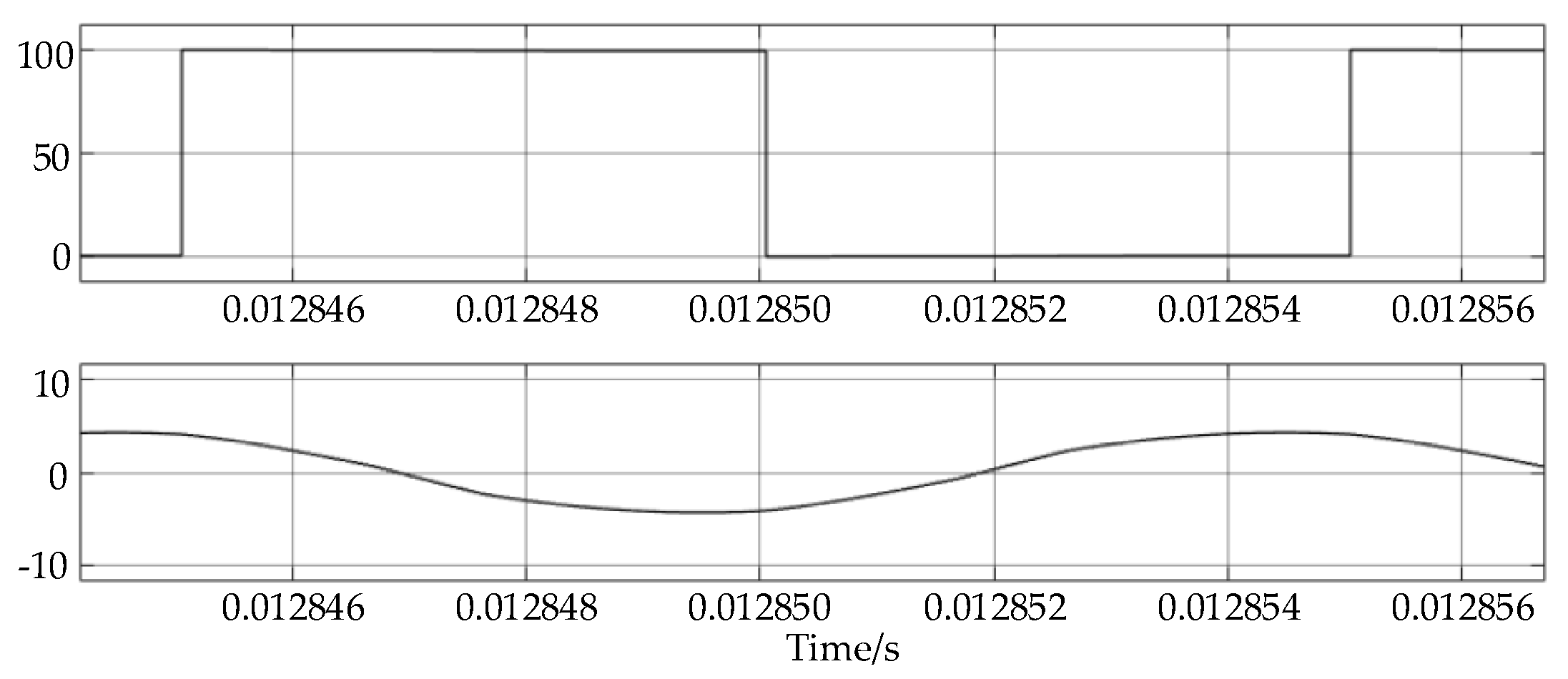
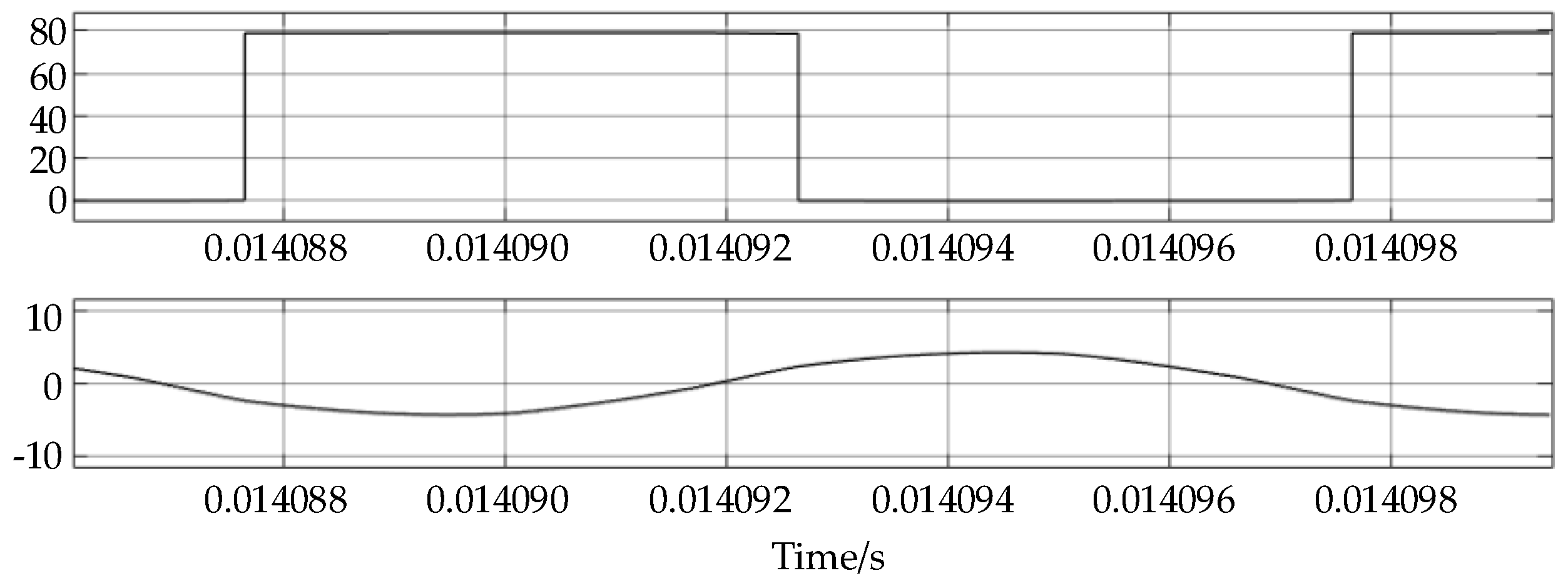
Observe the ZVS of each bridge arm, as shown in Figure 21, Figure 22 and Figure 23 below.
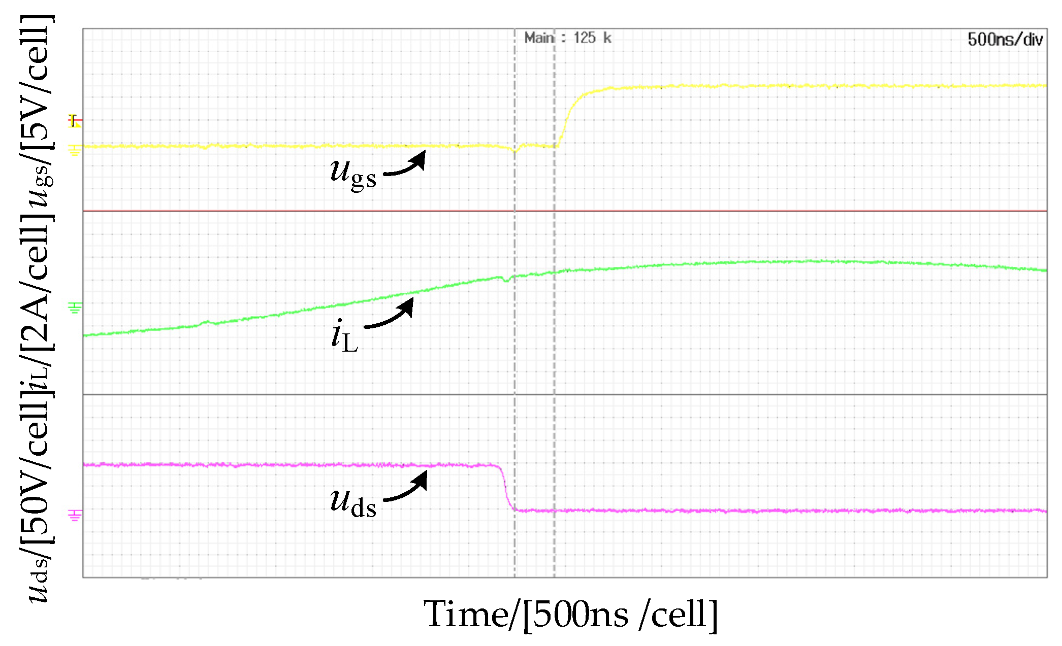
When full-arm ZVS is achieved, the A-arm current changes from negative to positive after the A-arm drain-source voltage drops to 0. The B-arm current changes from positive to negative after the B-arm drain-source voltage drops to 0. The C-arm current changes from negative to positive after the C-arm drain-source voltage drops to 0.
A combination of phase-shift angles within the ZVS range of the two full-bridge arms was randomly selected for the same power and gain, and the phase-shift angles (φAD = 97.2°, φAB = 115°) were chosen for the comparison of reactive power values, as shown in Figure 24.
The selected phase-shift angles (φAD = 31°, φAB = 80.2°) for the comparison of reactive power values is shown in Figure 25.
From the above simulation results, it can be seen that the reactive power value of the obtained phase-shift angle is significantly smaller than other combinations of phase-shift angles under the premise of achieving full-bridge arm ZVS. Although the obtained points may be located near the boundary of the A-bridge arm or B-bridge arm, the obtained results are located within the ZVS range, and the value of the reactive power is greatly reduced, which improves the overall efficiency of the system.
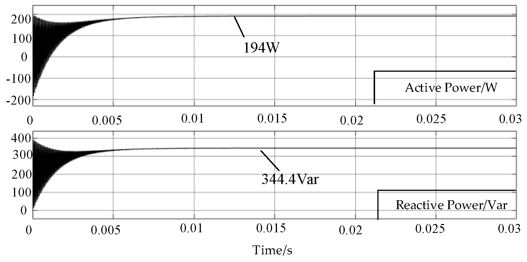
When the gain M = 0.8, the combination of phase-shift angles output from the flow chart is brought into the simulation, and the combination of phase-shift angles is (92°, 239°), the simulation results of the active and reactive power obtained are as shown in Figure 26.
Observe the ZVS of each bridge arm as shown in Figure 27, Figure 28 and Figure 29 below.
When the full-arm ZVS is realized, the resonant current turns from negative to positive after the A-arm drain-source voltage drops to 0. After the B-arm drain-source voltage drops to 0, the resonant current is at the positive to negative boundary, and the B-bridge arm is at the soft-switching boundary at this time. After the C-bridge arm drain-source voltage drops to 0, the transformer secondary current turns from negative to positive.
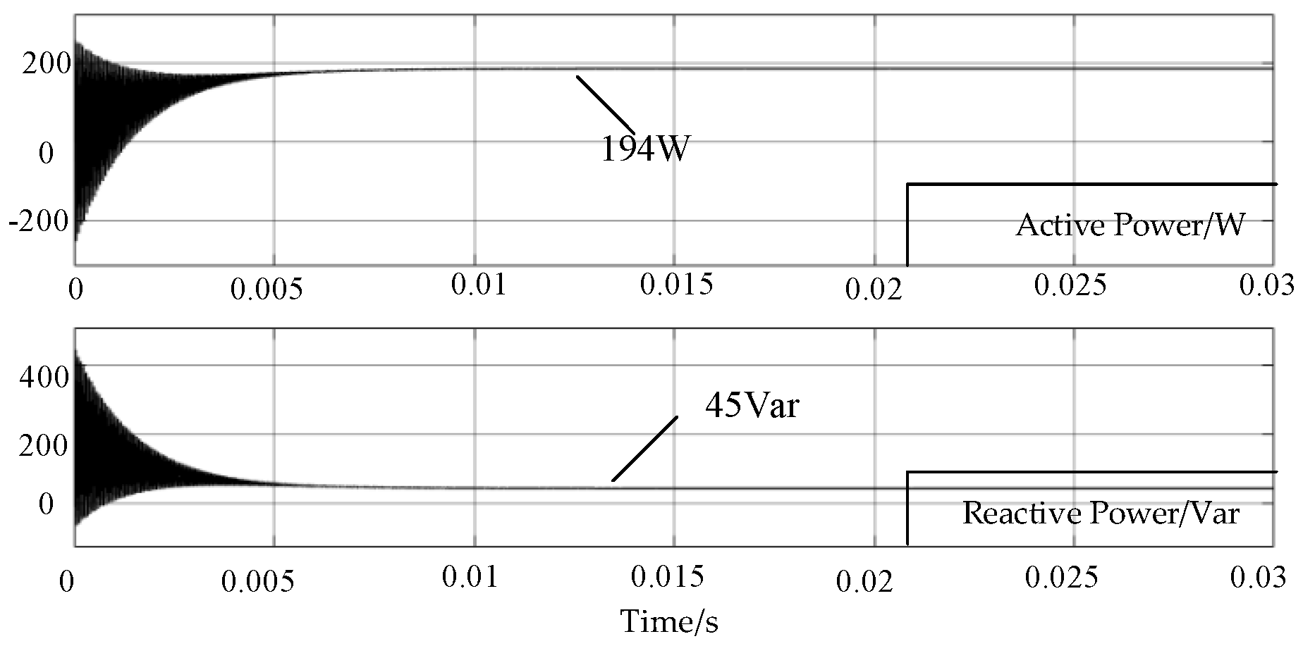
In the ZVS range of the full-bridge arm, a combination of phase-shift angles with the same power and gain was randomly selected and the phase-shift angle (φAD = 63°, φAB = 202.57°) was chosen to compare the reactive power values, as shown in Figure 30.
When the gain M = 0.8, it can be seen from the above simulation results that the reactive power value of the obtained phase-shift angle is significantly smaller than another set of phase-shift angle combinations under the premise of realizing the full-bridge arm ZVS, which improves the system efficiency.
When the gain M = 0.6, the simulations were performed for the combination of phase-shift angles (96.3°, 192°) and randomly selected phase-shift angles (92.4°, 195°) of the system output in the full-bridge arm ZVS range to compare the reactive power values, as shown in Figure 31 and Figure 32.
When the gain M = 0.6, it can be seen from the simulation results in Figure 31 and Figure 32 that the system output phase-shift angle combination has a smaller value of reactive power compared with the randomly selected phase-shift angle combination, so it can be proved that the system output phase-shift angle combination is more efficient.
From the above simulation, it can be seen that whether the gain M is less than 1 or the gain M is equal to 1, the reactive power output by the system with the combination of phase-shift angles is smaller than the combination of phase-shift angles randomly selected under the premise of satisfying the full-bridge arm ZVS, so the correctness of the control strategy can be proved.
According to the flowchart prepared in MATLAB, the simulation results for active power of 200 W for different output voltage ranges and for an output voltage of 100 V for different power cases were measured, as shown in Table 3 and Table 4.

4. Experimental Verification

Using the parameters given in Table 5, a test prototype was built for experimental verification of the theoretical analysis.
During the experiments, several different sets of phase-shift angles were selected for the experiments. Due to the need to ensure the safety of the experiments during the design process, the output current quickly reached the current limit value when the combination of phase-shift angles with larger values of reactive power were selected, which also confirms that the larger the reactive power, the lower the system efficiency. Therefore, the selected combinations of phase-shift angles are near the reactive power minimum point.
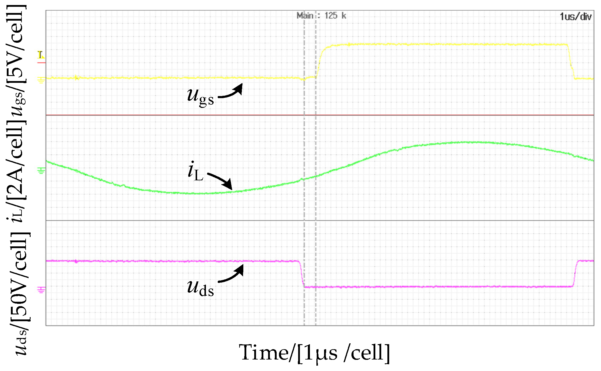
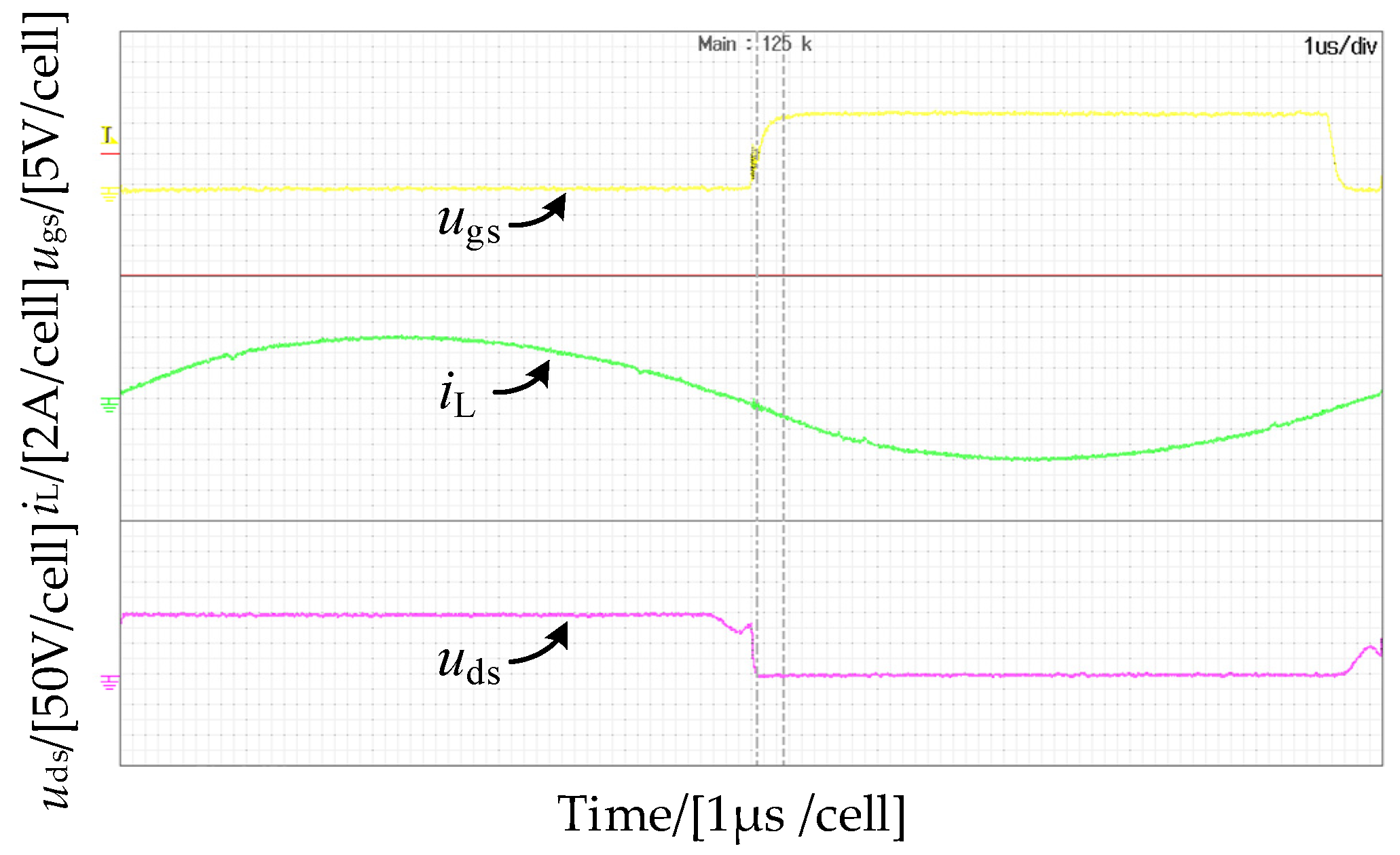
Firstly, the combination of phase-shift angle of the system output was used in the experiment. When the combination of inter-bridge phase-shift angle φAD and intra-bridge phase-shift angle φAB was (57°, 213°), the soft-switching waveforms of bridge-arm A, bridge-arm B and bridge-arm C were obtained, as shown in Figure 33, Figure 34 and Figure 35. In the figures, channel 1 is the driving voltage, channel 2 is the resonant current and channel 3 is the drain source voltage.
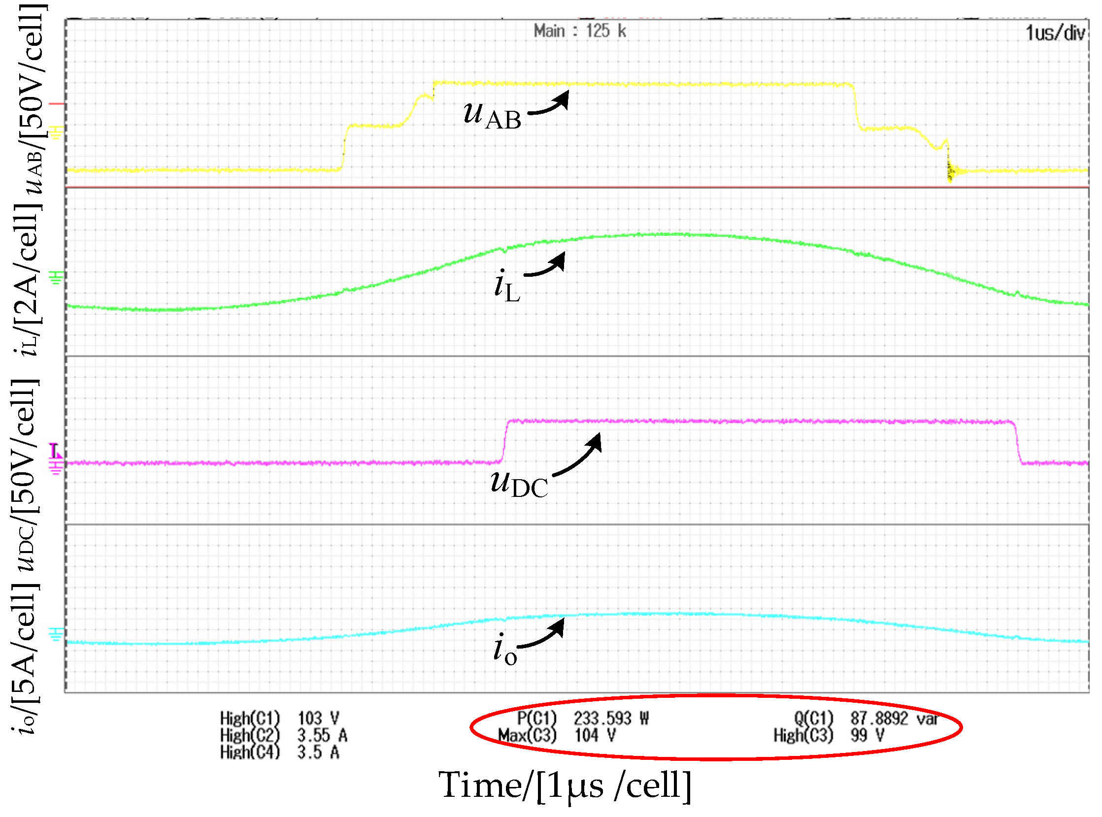
The waveforms of reactive power and active power are shown in Figure 36, where channel 1 is the voltage uAB waveform at the midpoint of the two bridge arms on the primary side, channel 2 is the resonant current waveform, channel 3 is the voltage uDC waveform at the midpoint of the two bridge arms on the secondary side and channel 4 is the output current waveform.
It can be seen that the combination of the phase-shift angle of the output of the reactive power flow diagram is located near the soft-switching boundary of the B-bridge arm, but the parasitic parameters of the switching device and transformer are not considered in the simulation. However, in the actual experimental process, the parasitic parameters of the PCB board and the switching device and other factors affect the circuit operation, resulting in the actual experimental results of the B-bridge arm not achieving soft-switching; in the actual simulation, because the transformer is the ideal case, the simulation of the B-bridge arm achieves ZVS soft switching, resulting in deviations between the theoretical simulation results and the actual experimental results.
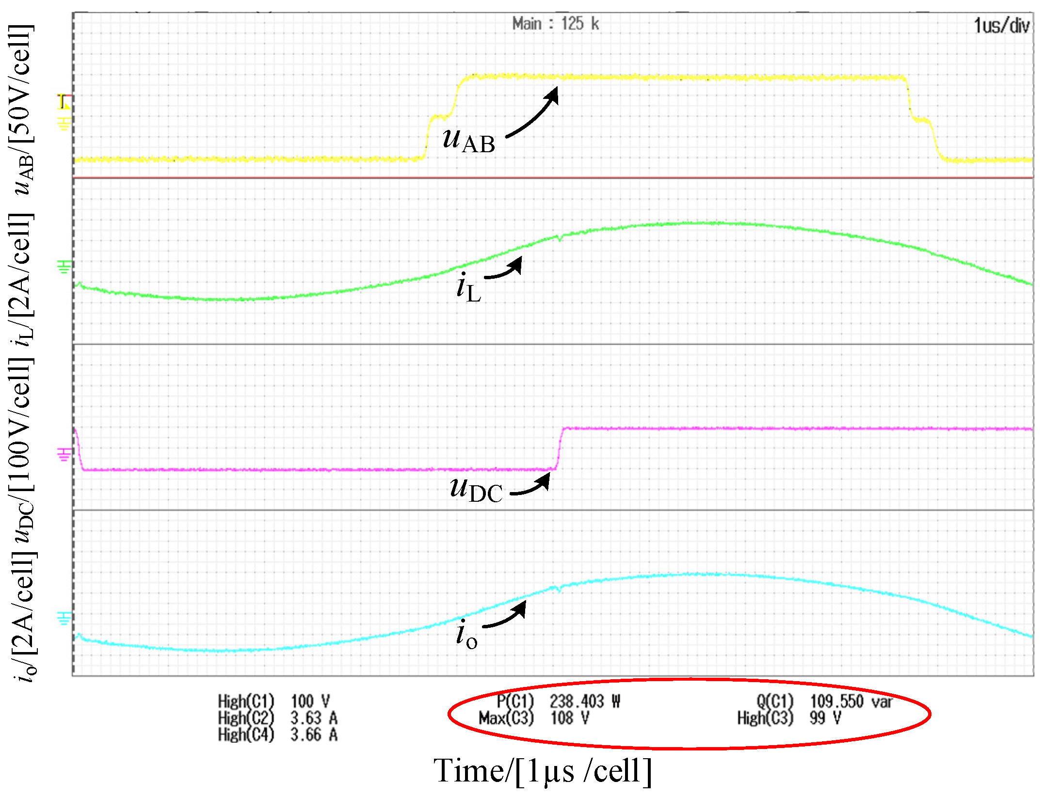
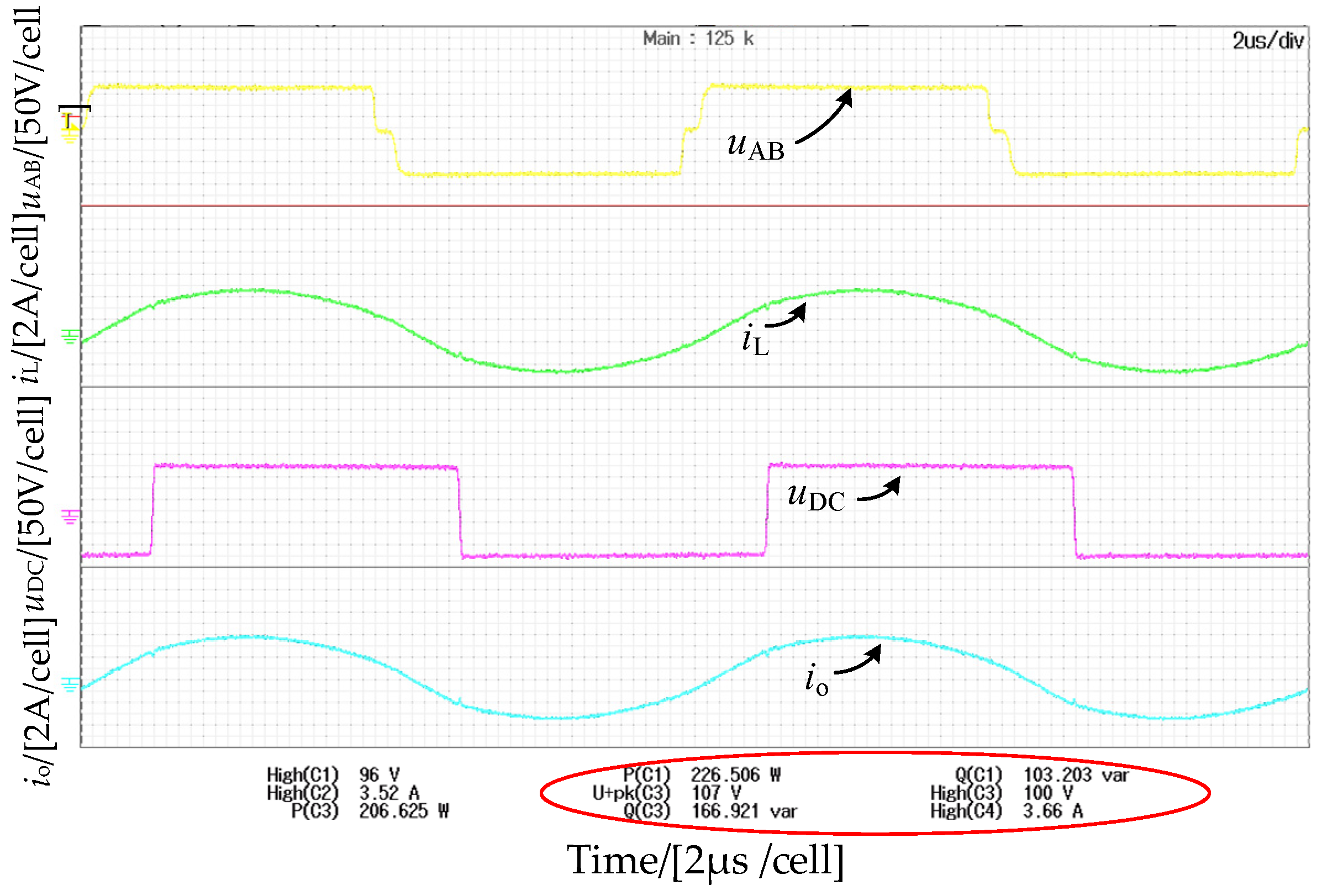
When the combination of inter-bridge phase-shift angle φAD and intra-bridge phase-shift angle φAB is (40°, 171°) and the combination of inter-bridge phase-shift angle φAD and intra-bridge phase-shift angle φAB is (49°, 190°), the obtained active and reactive power waveforms are as shown in Figure 37 and Figure 38.
From the above experimental waveform diagram, it can be seen that the reactive power of the phase-shift angle combination output by the flow chart is smaller than the reactive power of the randomly selected phase-shift angle, and it can be learned from the calculated efficiency that the system efficiency is the highest for the phase-shift angle combination output by the flow chart. The transmission efficiencies of the three phase-shift angle combinations are calculated for an output power of 200 W, as shown in Table 6.

5. Conclusions

In this paper, a reactive power-minimization control strategy is proposed with the topology of series-resonant DAB, EPS is analytically selected as the modulation method and the reactive power of the system is reduced as the objective, with the realization of full-bridge arm ZVS as the premise. By analyzing and studying the objective function, the reactive power-minimization control algorithm is designed and the optimization flow chart is drawn, and the two cases of gain M less than and M equal to 1 are verified by simulation. The simulation results from Figure 31 and Figure 32 show that when the gain M = 0.6, the reactive power value of the system output phase-shift angle combination is 10 Var smaller than the reactive power of the randomly selected phase-shift angle combination. The simulation results from Figure 26 and Figure 30 show that when the gain M = 0.8, the reactive power value of the system output phase-shift angle combination is 11.7 Var smaller than the reactive power of the randomly selected phase-shift angle combination. The case of gain M = 1 was verified experimentally, and as can be seen from the data in Table 6, the reactive power values at the output of the system were reduced by 22.7 Var and 16.4 Var compared to two randomly chosen combinations of phase-shift angles. Therefore, it can be proved that the control strategy can effectively improve the system efficiency.

Author Contributions

Conceptualization, investigation, supervision, project administration and funding acquisition, J.W. and X.S. (Xiaofeng Sun); re-sources, methodology, software, validation and writing—original draft preparation, W.Z.; formal analysis and data curation, X.S. (Xinyu Su). All authors have read and agreed to the published version of the manuscript.

Funding

This work was supported in part by the Nature Science Foundation of Heibei Province under Grant E2021, and in part by the Key Research and Development Program of Hebei Province under Grant 19214405D.

Institutional Review Board Statement

Not applicable.

Informed Consent Statement

Not applicable.

Data Availability Statement

Not applicable.

Conflicts of Interest

The authors declare no conflict of interest.

References

  1. De Doncker, R.W.; Divan, D.M.; Kheraluwala, M.H. A three-phase soft-switched high-power-density DC/DC converter for high-power applications. IEEE Trans. Ind. Appl. 1991, 27, 63–73. [Google Scholar] [CrossRef]
  2. Zhao, B.; Song, Q.; Liu, W.; Sun, Y. Dead-Time Effect of the High-Frequency Isolated Bidirectional Full-Bridge DC–DC Converter: Comprehensive Theoretical Analysis and Experimental Verification. IEEE Trans. Power Electron. 2014, 29, 1667–1680. [Google Scholar] [CrossRef]
  3. Zhao, B.; Yu, Q.; Sun, W. Extended-Phase-Shift Control of Isolated Bidirectional DC–DC Converter for Power Distribution in Microgrid. IEEE Trans. Power Electron. 2012, 27, 4667–4680. [Google Scholar] [CrossRef]
  4. Verma, V.; Gupta, A. Performance enhancement of the Dual Active Bridge with dual phase shift control and variable frequency modulation. In Proceedings of the IEEE International Conference on Power Electronics, Drives and Energy Systems, Trivandrum, India, 14–17 December 2016; pp. 1–6. [Google Scholar]
  5. Zhao, B.; Song, Q.; Liu, W.; Sun, Y. Overview of Dual-Active-Bridge Isolated Bidirectional DC-DC Converter for High-Frequency-Link Power-Conversion System. IEEE Trans. Power Electron. 2014, 29, 4091–4106. [Google Scholar] [CrossRef]
  6. Zhao, B.; Yu, Q.; Sun, W. Bi-directional Full-bridge DC-DC Converters With Dual-phase-shifting Control and Its Backflow Power Characteristic Analysis. Proc. CSEE 2012, 32, 43–50. [Google Scholar]
  7. Shi, Y.; Li, R.; Xue, Y.; Li, H. Optimized Operation of Current-Fed Dual Active Bridge DC–DC Converter for PV Applications. IEEE Trans. Ind. Electron. 2015, 62, 6986–6995. [Google Scholar] [CrossRef]
  8. Han, W.; Ma, R.; Liu, Q.; Corradini, L. A conduction losses optimization strategy for DAB converters in wide voltage range. In Proceedings of the IECON 2016—42nd Annual Conference of the IEEE Industrial Electronics Society, Florence, Italy, 23–26 October 2016; pp. 2445–2451. [Google Scholar]
  9. Sun, X.; Wang, H.; Qi, L.; Liu, F. Research on Single Stage High Frequency Link SST Topology and Its Optimization Control. IEEE Trans. Power Electron. 2020, 35, 8701–8711. [Google Scholar] [CrossRef]
  10. Wen, H.; Chen, J. Control and efficiency optimization of Dual-Active-Bridge DC/DC converter. In Proceedings of the 2016 IEEE International Conference on Power Electronics, Drives and Energy Systems (PEDES), Trivandrum, India, 14–17 December 2016; pp. 1–6. [Google Scholar]
  11. Liu, B.; Davari, P.; Blaabjerg, F. An Optimized Control Scheme to Reduce the Backflow Power and Peak Current in Dual Active Bridge Converters. In Proceedings of the 2019 IEEE Applied Power Electronics Conference and Exposition (APEC), Anaheim, CA, USA, 17–21 March 2019; pp. 1622–1628. [Google Scholar]
  12. Bai, H.; Mi, C. Eliminate Reactive Power and Increase System Efficiency of Isolated Bidirectional Dual-Active-Bridge DC-DC Converters Using Novel Dual-Phase-Shift Control. IEEE Trans. Power Electron. 2008, 23, 2905–2914. [Google Scholar] [CrossRef]
  13. Wen, H.; Xiao, W.; Su, B. Nonactive Power Loss Minimization in a Bidirectional Isolated DC–DC Converter for Distributed Power Systems. IEEE Trans. Ind. Electron. 2014, 61, 6822–6831. [Google Scholar] [CrossRef]
  14. Shi, H.; Wen, H.; Chen, J.; Hu, Y.; Jiang, L.; Chen, G. Minimum-Reactive-Power Scheme of Dual Active Bridge DC-DC Converter With 3-Level Modulated Phase-Shift Control. IEEE Trans. Ind. Appl. 2017, 53, 5573–5586. [Google Scholar] [CrossRef] [Green Version]
  15. Tong, A.; Hang, L.; Li, G.; Jiang, X.; Gao, S. Modeling and Analysis of a Dual-Active-Bridge-Isolated Bidirectional DC-DC Converter to Minimize RMS Current With Whole Operating Range. IEEE Trans. Power Electron. 2018, 33, 5302–5316. [Google Scholar] [CrossRef]
  16. Li, X.; Bhat, A.K.S. Analysis and Design of High-Frequency Isolated Dual-Bridge Series Resonant DC/DC Converter. IEEE Trans. Power Electron. 2010, 25, 850–862. [Google Scholar]
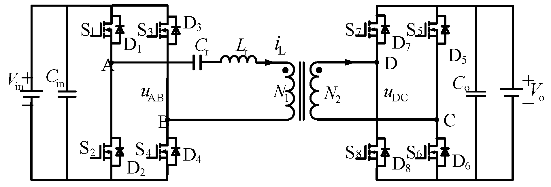
Figure 1. Series-resonant-type dual-active-bridge converter topology.
Energies 15 03856 g001
Figure 2. Series-connected resonant dual-active-bridge converter equivalent circuit diagram.
Energies 15 03856 g002
Figure 3. Work waveform under EPS modulation.
Energies 15 03856 g003
Figure 4. Work waveform under DPS modulation.
Energies 15 03856 g004
Figure 5. Work waveform under TPS modulation.
Energies 15 03856 g005
Figure 6. ZVS area under EPS modulation.
Energies 15 03856 g006
Figure 7. ZVS area under DPS modulation.
Energies 15 03856 g007
Figure 8. Closeroen arm ZVS area under TPS modulation.
Energies 15 03856 g008
Figure 9. Intersection of active power and reactive power contours under EPS modulation (M = 1).
Energies 15 03856 g009
Figure 10. Intersection of active power and reactive power contours under DPS modulation (M = 1).
Energies 15 03856 g010
Figure 11. Intersection of active power and reactive power contours under TPS modulation (M = 1).
Energies 15 03856 g011
Figure 12. PEPS.pu = 0.67 at different gain M, the relation curve between QEPS.pu and the bridge phase-shift angle φAD.
Energies 15 03856 g012
Figure 13. The relation curve between QEPS.pu and the bridge phase-shift angle φAD under different monoid values of active power.
Energies 15 03856 g013
Figure 14. φAD = 30°, φAB = 76.9° active power and reactive power waveforms.
Energies 15 03856 g014
Figure 15. φAD = 30° and φAB = 163.1° active power and reactive power waveforms.
Energies 15 03856 g015
Figure 16. φAD = 90° and φAB = 103° active power and reactive power waveforms.
Energies 15 03856 g016
Figure 17. φAD = 90° and φAB = 257° active power and reactive power waveforms.
Energies 15 03856 g017
Figure 18. Intersection of different active power standardized values and reactive contour.
Energies 15 03856 g018
Figure 19. Reactive power minimization optimization seeking control flow.
Energies 15 03856 g019
Figure 20. φAD = 25.8° and φAB = 152° active power and reactive power waveforms.
Energies 15 03856 g020
Figure 21. φAD = 25.8° and φAB = 152° bridge-arm A drain-source voltage and current waveforms.
Energies 15 03856 g021
Figure 22. φAD = 25.8° and φAB = 152° bridge-arm B drain-source voltage and current waveforms.
Energies 15 03856 g022
Figure 23. φAD = 25.8° and φAB = 152° bridge-arm C drain-source voltage and current waveforms.
Energies 15 03856 g023
Figure 24. φAD = 97.2° and φAB = 115° active power and reactive power waveforms.
Energies 15 03856 g024
Figure 25. φAD = 31° and φAB = 80.2° active power and reactive power waveforms.
Energies 15 03856 g025
Figure 26. φAD = 92° and φAB = 239° active power and reactive power waveforms.
Energies 15 03856 g026
Figure 27. φAD = 92° and φAB = 239° bridge-arm A drain-source voltage and current waveforms.
Energies 15 03856 g027
Figure 28. φAD = 92° and φAB = 239° bridge-arm B drain-source voltage and current waveforms.
Energies 15 03856 g028
Figure 29. φAD = 92° and φAB = 239° bridge-arm C drain-source voltage and current waveforms.
Energies 15 03856 g029
Figure 30. φAD = 63° and φAB = 202.57° active power and reactive power waveforms.
Energies 15 03856 g030
Figure 31. φAD = 96.3° and φAB = 192° active power and reactive power waveforms.
Energies 15 03856 g031
Figure 32. φAD = 92.29° and φAB = 185° active power and reactive power waveforms.
Energies 15 03856 g032
Figure 33. Bridge-arm A soft-switching waveform diagram.
Energies 15 03856 g033
Figure 34. Bridge-arm B soft-switching waveform diagram.
Energies 15 03856 g034
Figure 35. Bridge-arm C soft-switching waveform diagram.
Energies 15 03856 g035
Figure 36. φAD = 57° and φAB = 213° experimental waveforms with reactive power optimization control.
Energies 15 03856 g036
Figure 37. φAD = 40° and φAB = 171° experimental waveforms without reactive power optimization.
Energies 15 03856 g037
Figure 38. φAD = 49° and φAB = 190° experimental waveforms without reactive power optimization.
Energies 15 03856 g038
Table 1. The normalized value of active power and the minimum reactive power intersection value.
The Normalized Values of Active Power0.10.20.30.40.50.60.70.80.9
Minimum reactive power valueEPS00.0180.050.070.120.200.270.390.52
DPS00.020.050.080.130.210.290.40.55
TPS0.40.620.770.911.6
Table 2. Comparison of reactive power values at different phase-shift angles.
Inter-Bridge Phase-Shift Angle φAD (°)Intra-Bridge Phase-Shift Angle φAB1 (°)Reactive Power QEPS.pu1 (Var)Intra-Bridge Phase-Shift Angle φAB2 (°)Reactive Power QEPS.pu2 (Var)
3076.9100163.165
6081.920021957
9010334025743
120141.34495278.6667
150196.88539283.12146
Table 3. Optimal combination of phase-shift angle at 200 W output power and 50–100 V output voltage.
The Output Voltage (V)Inter-Bridge Phase-Shift Angle φAD (rad)Intra-Bridge Phase-Shift Angle φAB (rad)
502.0944.002
601.6833.352
701.5163.789
801.6124.180
901.2924.012
1000.9903.722
Table 4. Output voltage 100 V output power 100 W–200 W change optimal phase-shift angle combination table.
Output Power (W)Inter-Bridge Phase-Shift Angle φAD (rad)Intra-Bridge Phase-Shift Angle φAB (rad)
1500.6963.550
1600.7503.582
1700.8063.614
1800.8653.649
1900.9253.684
2000.9903.722
Table 5. Main circuit parameters of the experimental prototype.
Parameter NameParameter Value
Input Voltage Vin100 V
Output Voltage Vo100 V
Switching Frequency fs(Hz)100 kHz
Transformer Ratio1:1
Resonant Inductor146 μH
Resonant Capacitor24 nF
Rated Power200 W
Dead Time200 ns
MOSFET20N60C3
Table 6. Reactive power when the transmitted power is 200 W.
Output PowerPhase-Shift Angle CombinationReactive Power Value
200 W(57°, 213°)86.8 Var
(40°, 171°)109.5 Var
(49°, 190°)103.2 Var
Publisher’s Note: MDPI stays neutral with regard to jurisdictional claims in published maps and institutional affiliations.