Article

An Overview about Si, Superjunction, SiC and GaN Power MOSFET Technologies in Power Electronics Applications

by
Edemar O. Prado
1,2,*,
Pedro C. Bolsi
1,2,
Hamiltom C. Sartori
2 and
José R. Pinheiro
1,2
1
Energy Efficiency Lab, LABEFEA, Federal University of Bahia, Salvador 40170-110, BA, Brazil
2
Power Electronics and Control Research Group, GEPOC, Federal University of Santa Maria, Santa Maria 97105-900, RS, Brazil
*
Author to whom correspondence should be addressed.
Energies 2022, 15(14), 5244; https://doi.org/10.3390/en15145244
Submission received: 17 June 2022 / Revised: 7 July 2022 / Accepted: 12 July 2022 / Published: 20 July 2022

Abstract

:
This work presents a comparative analysis among four power MOSFET technologies: conventional Silicon (Si), Superjunction (SJ), Silicon Carbide (SiC) and Gallium Nitride (GaN), indicating the voltage, current and frequency ranges of the best performance for each technology. For this, a database with 91 power MOSFETs from different manufacturers was built. MOSFET losses are related to individual characteristics of the technology: drain-source on-state resistance, input capacitance, Miller capacitance and internal gate resistance. The total losses are evaluated considering a drain-source voltage of 400 V, power levels from 1 kW to 16 kW (1 A–40 A) and frequencies from 1 kHz to 500 kHz. A methodology for selecting power MOSFETs in power electronics applications is also presented.

Graphical Abstract

1. Introduction

The increasing volumetric power density in static converters is a subject that has been highlighted in recent decades [1,2,3,4,5,6,7]. The expansion of the renewable energy and electric vehicle sectors increases the need for high power density and high performance in static converters [8,9,10,11,12]. Applications with higher switching frequencies are indicated as a possible way to reduce the volume of passive components. However, increasing switching frequency results in higher switching losses in power transistors, which may reduce the efficiency of converters and increase the volume and cost of heat transfer systems [13,14,15,16].
In order to reduce electrical losses, the industry began to develop power MOSFETs using different semiconductor structures and technologies, improving their performance at higher frequencies, powers and drain-source voltages [17,18,19,20,21]. For silicon-based devices, the structure was modified, resulting in the development of superjunction (SJ) devices. These devices present a significant reduction in the drain-source on-state resistance, shorter switching times and increases in the drain-source breakdown voltage capability [17,19,22,23,24].
The development of wide bandgap technologies, such as Silicon Carbide (SiC) and Gallium Nitride (GaN), also enable operation at higher frequencies [17,18,19,20,21,25]. Physical characteristics of SiC technology, such as high thermal conductivity, high electric field and wide energy gap, make its use attractive for applications where it is necessary to operate at higher temperatures, frequencies, powers and high drain-source voltages [18,26,27,28,29]. GaN technology has an electric field and energy gap similar to SiC devices, with greater electron mobility and lower thermal conductivity [26,28,30]. Electron mobility reduces switching times and output capacitance. For this reason, GaN technology tends to present an advantage in high-frequency operations. A lower thermal conductivity, on the other hand, provides disadvantages in situations where there is a need to operate at higher powers and temperatures [17,18,28,30,31,32].
In power electronics applications, a vertical MOSFET structure is preferable. This ensures uniform current distribution in the transistor. While GaN theoretically offers better high-frequency and high-voltage performances, the lack of good-quality bulk substrates required for vertical devices and the lower thermal conductivity of GaN give SiC the best position for high voltages. Because of this, some limitations in the vertical structures of the GaN FETs have been reported; although bearing the same previous FET structure, these devices have low blocking voltages (approximately 65 V), making their applications at higher powers unfeasible [20,21,26,31]. The GaN HEMT (high electron mobility transistor) with lateral structure is commonly used in this situation [20,21,31,32]. Although the GaN HEMT structure has a normally on behavior, several techniques have been developed to provide a modification in order to obtain a normally off behavior in the device, but intrinsic characteristics of the materials led to failures [32]. To easily apply GaN HEMT in circuit design, a low-voltage Silicon MOSFET is connected in series to provide normally off behavior. This structure is known as a cascode structure [20,21,31,32,33].
The development of power MOSFET technologies brings the challenge of defining which technologies and part numbers perform best in defined applications of drain-source voltage, current levels and switching frequencies. In the last decade, authors have analyzed the behavior of losses in different power MOSFET technologies [20,34,35,36,37,38,39,40,41,42,43,44,45]. Overall, losses were presented for specific operating points as in [34,36,37,40,42,43,45], specific part numbers [20,34,35,37,38,39,40,41] or for part numbers of different technologies and the same manufacturer [44].
In order to make a fair comparison among technologies, losses need to be estimated with accuracy. They may be calculated by analytical methods, SPICE, or finite element analysis (FEA) [16,46,47,48,49]. Due to its simplicity and processing time, the use of analytical models is preferable when reduced computational time is required [38,47,48,50]. In this work, the model proposed by [16] is used to estimate switching losses. Among the models [16,51,52,53,54,55,56], only [16,52] considered the internal gate resistance in loss calculation, while [16] also takes into account Miller capacitance variation and gate driver characteristics to determine overlap times. The DC link voltage used was 400 V. This voltage level is commonly used in literature for motor drive electric vehicle applications [11,57], in the design of step-up converters [3,13,58] and for microgrid applications [59,60,61].
Based on the outlined discussions, this paper presents four main contributions:
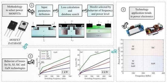
  • A comparative analysis among four power MOSFET technologies: conventional Silicon (Si), Superjunction (SJ), Silicon Carbide (SiC) and Gallium Nitride (GaN) using a database with 91 part numbers from different manufacturers (Appendix A);
  • A correlation of losses to physical characteristics of each technology, considering internal capacitances, internal gate resistances and drain-source on-state resistance as a function of junction temperature;
  • A methodology for selecting power MOSFETs in power electronics applications;
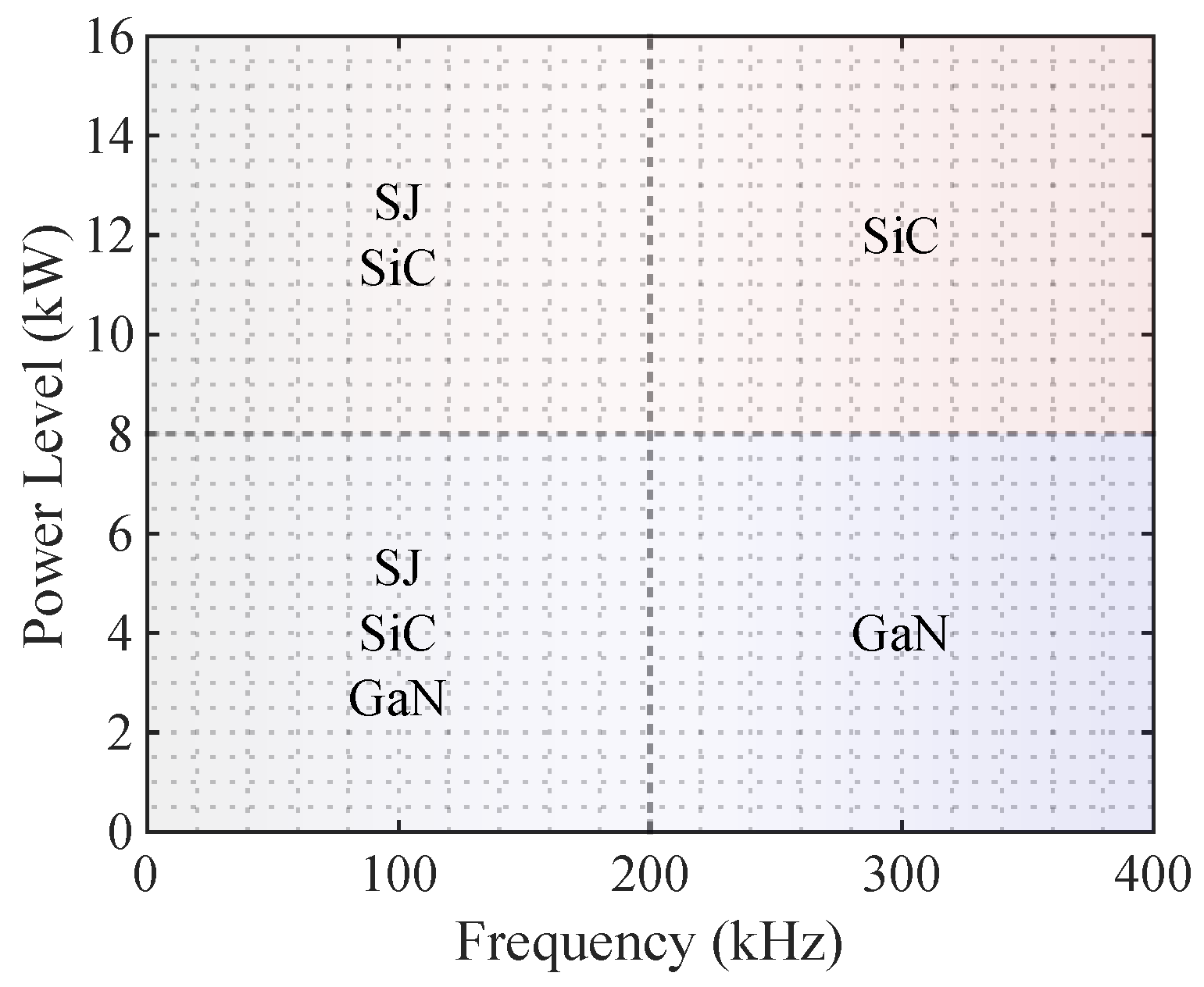
  • A definition of power and frequency ranges of the best performance for each technology, considering a drain-source voltage of 400 V, power levels from 1 kW to 16 kW (1 A–40 A) and frequency ranges from 1 kHz to 500 kHz.

2. Losses in Power MOSFETs

The equations of [16] are presented below and are used in the analysis presented in Section 4. The analytical model for obtaining the power dissipated during on-state period of MOSFETs ( P C ) relates the square of RMS current with the on-state drain-to-source resistance ( R D S o n ), considering junction temperature ( T J ) for a specific operation point:
P C = R D S o n ( T j ) I R M S 2 .
Switching losses are estimated by:
P S W = 1 2 ( t o n V D S I o n + t o f f V D S I o f f ) F S W
where F S W is the switching frequency, V D S is the drain-to-source voltage over the MOSFET and I o n , I o f f and t o n , t o f f are the respective currents and overlap times of MOSFET turn-on and turn-off.
Time periods t o n and t o f f are determined as:
t o n = Q I G o n
t o f f = Q I G o f f
Q being the total charge, and I G o n and I G o f f the gate currents at turn-on and turn-off:
I G o n = ( V G S V P L ) / R G
I G o f f = V P L / R G
in which V G S and V P L are the gate and plateau voltages, and R G corresponds to the combination of external and internal gate resistances ( R G = R G e x t + R G i n t ).
Q is given by the sum of gate-source and gate-drain charges, Q G S and Q G D :
Q = Q G S + Q G D
Q G S = C I S S ( V P L V T H )
Q G D = C G D ( B ) V D S + C G D ( A ) 0.135 V D S 2
in which C I S S is the input capacitance, and C G D ( A ) and C G D ( B ) are the gate-to-grain capacitances obtained at different points of the C G D × V D S curve, as explained in [16].
With these definitions, total losses are obtained by adding Equations (1) and (2):
P T O T = P C + P S W .

3. Analytical Model Experimental Validation

The analytical model used as a basis for the comparative analysis is validated using the test circuit shown in Figure 1. It operates in steady-state and thermal equilibrium. This disregards the thermal transients of the MOSFET, and the temperature on the device may be considered uniform [62].
The tested MOSFETs were MTW20N50E (Si), IPW60R040C7 (SJ) and IMW65R072M1H (SiC). These were operated at voltages corresponding to 40%, 50% and 60% of each respective drain-source breakdown voltage ( V D S b ). The switching frequencies used were 50 kHz and 150 kHz. Circuit parameters considered include: R G = 15 Ω , V G S = 15 V, R L = 70 Ω and L = 1.7 mH. In order to minimize the effects of reverse recovery, a freewheeling diode C3D10060A of SiC technology was used.
For temperature measurements, a Fluke Ti20 thermal camera was used. This thermal imaging device has a accuracy of ±2 C or 2%, whichever is the highest [63]. The thermal camera emissivity was set to 0.9. Ambient temperature was constant for each test, and the laboratory environment was kept separate from external interference in temperature, such as wind or other nearby heat sources. Thermal results obtained in this evaluation are shown in Figure 2a–c for Si, SJ and SiC technologies, respectively, where the measured point is the package of MOSFET under test, and the scale of the thermal camera is adjusted automatically.
From the temperature, total losses were obtained using the thermal resistances of each device. Using the data of R θ C A from [16] and the measured ambient and case temperatures, losses can be found for each evaluated condition [62,64,65]:
P T O T = T C T A R θ C A .
The comparison among measured and calculated losses and its associated error is shown in Table 1. The largest errors were 6.63% for Si technology, 5.65% for SJ technology and 6.9% for SiC technology. The results obtained validate the analytical model for each technology, in different voltage ratings and switching frequencies. The behavior of the Miller capacitance in GaN cascode devices is similar to the other technologies of power MOSFETs, presenting two different characteristics in the Miller capacitance curve shape. In low voltages there is a high variation of capacitance with voltage, and after that, a more linear behavior [16]. Based on this characteristic, the model represents switching losses accurately for GaN FETs as well.

4. Impact of Internal Parameters on MOSFET Losses

4.1. Conduction Loss Evaluation

As shown in Section 2, conduction losses in power MOSFETs are a function of R D S o n (dependent on T J ) and the RMS current. The flowchart in Figure 3 shows the methodology used to evaluate conduction losses, summarized in 5 steps:
  • Step 1: The initial RMS current of 1 A and T J of 25 C and 125 C are defined.
  • Step 2: The algorithm searches the database, selecting transistors that meet the current capacity criteria for the specified current.
  • Step 3: The losses are calculated by Equation (1).
  • Step 4: In each current iteration, the part number that presents the lowest losses for each technology is selected. This procedure is executed in steps of 1 A until the RMS current reaches 100 A. Thus, it is possible to select different part numbers for the same technology along the current range.
  • Step 5: As the output, the behavior of the conduction losses with current variation is obtained.
In addition to T J , V G S has also a direct impact on R D S o n . Therefore, R D S o n is adjusted according to the applied gate voltage, following the electrical characteristics diagrams from each MOSFET datasheet. In order to operate all technologies close to saturation region, the gate voltage used was 18 V.
The results are shown in Figure 4, where solid lines represent the conduction losses at T J = 25 C and dashed lines represent the losses calculated for T J = 125 C; line colors identify each technology.
For conduction losses in 25 C, SiC, SJ and GaN technologies present similar losses up to the range of I R M S = 20 A, above this value, SiC technology presents the best performance. GaN and SJ technologies presents similar losses, but higher than SiC, with the maximum rated RMS current for GaN technology being 91 A. Silicon MOSFETs present the highest losses (highest R DSon ), and their rated RMS current is limited to 49 A. As the temperature is increased from 25 C to 125 C, SiC presented the lowest losses compared to other technologies in the RMS current range above 20 A. The Si rated RMS current is limited to 40 A, GaN to 58 A, SJ to 68 A and SiC to 95 A. The rated current limits are obtained from the database presented in Appendix A.
To visualize the impact of T J variation on R D S o n , in Figure 5 the averages of normalized values of R D S o n for each technology are shown ( R D S o n ( N o r m ) = R D S o n ( T j ) / R D S o n ( 25 ) ). These values are obtained by running temperature scans for all transistors in the database and averaging them for each technology. The increase in normalized values of R D S o n is the lowest in SiC when compared to the other technologies (around 50%). The largest variation in R D S o n ( N o r m ) occurs in the Si MOSFET, with an increase of 160% when varying T J from 25 C to 150 C. The SJ and GaN technologies increase by about 100%. The increase in R D S o n by T J variation has a significant impact on the transistor losses, as shown in Figure 4; thus, it may not be disregarded.

4.2. Switching Loss Evaluation

Switching losses are determined as defined in Section 2, being a function of R G e x t , V G S , I o n , I o f f , C I S S , C G D , V P L , V T H , R G i n t , V D S and F S W . Gate driver parameters ( V G S and R G e x t ) determine the charging and discharging of a transistor’s internal capacitances. From the internal parameters, C I S S is responsible for the rise and fall times of the current, while C G D is responsible for the rise and fall times of the voltage, which are significantly smaller than C I S S and highly nonlinear. V P L is the voltage at which C G D starts charging and also represents the end of gate-source charging. V T H is the voltage at which MOSFET enters the on-state region, and R G i n t is the internal gate resistance of the MOSFET. When MOSFETs are manufactured for different drain-source voltage ratings or different current levels, its characteristics are modified.
To determine the influence of the internal parameters on switching losses and to define application trends, two scenarios (evaluations) are considered. In the first scenario, (Section 4.2.1) the internal gate resistance R G i n t is disregarded, with the goal of demonstrating the impact of the internal capacitances in switching losses. In the second scenario (Section 4.2.2), results are obtained with R G i n t included. The external parameters to determine losses were considered as V D S = 400 V, R G e x t = 15   Ω , V G S = 18 V, average currents of 2.5 to 80 A and frequency range of 1 kHz to 500 kHz, as shown in the flowchart of Figure 6. The switching loss evaluation is summarized in 5 steps:
  • Step 1: Input parameters are set as I S W = I o n = I o f f = 2.5 A, V D S = 400 V and starting frequency = 1 kHz.
  • Step 2: The algorithm searches the database, selecting transistors that meet the current and voltage criteria.
  • Step 3: The losses are calculated by Equation (2).
  • Step 4: Only the transistor of each technology that presents lowest losses (for a set of parameters) is selected. Step 4 is performed in steps of 1 kHz until the switching frequency reaches 500 kHz, for current levels of 2.5 A until 80 A. The current loop is doubled in each iteration. It is possible to select different part numbers for the same technology along the frequency and current ranges.
  • Step 5: As the output, the behavior of losses with variations in the switching frequency and current levels in scenario 1 (without including R G i n t ) and scenario 2 (using R G i n t ) are obtained.

4.2.1. Scenario 1: Influence of Internal Capacitances

The results obtained for scenario 1 are shown in Figure 7 (a) for 2.5 A, (b) 5 A, (c) 10 A, (d) 20 A, (e) 40 A and (f) 80 A. In this analysis, the numerical behavior of the losses was evaluated. It disregards the junction temperature, considering only both V D S b and current capability.
Figure 7a shows a loss comparison considering V D S = 400 V and a current of 2.5 A. In this range, SJ MOSFET presented the lowest switching losses, followed by SiC and GaN. In Figure 7b, the SiC, SJ and GaN MOSFETs present the lowest switching losses, while the Si MOSFET has the highest losses. In Figure 7c, GaN presents the best performance, as well as in Figure 7d,e. In Figure 7f, only the SJ and SiC transistors met the current capacity criteria, and SiC presents the lowest losses. The part numbers that minimize switching losses for each current level, frequency and technology are shown in Table 2.
The behavior of losses for the selected power MOSFETs is related to the internal parameters of each part number and technology. Table 3, Table 4, Table 5 and Table 6 show the characteristics of R D S o n at 25 C, C I S S and C G D , for SJ, SiC, GaN and Si technologies, respectively, considering a drain-source voltage of 400 V.
In Table 3, Table 4, Table 5 and Table 6, it is possible to identify that in all cases, as the current levels increase, C I S S and C G D ( V D S ) also increase, while R D S o n ( 25 ) decreases. This occurs because, at higher current levels, to reduce R D S o n , manufacturers increase the carrier density and die size, which, as a consequence, increases the internal capacitances. Otherwise, at lower current levels, the die size is smaller, reducing the internal capacitances and increasing R D S o n .

4.2.2. Scenario 2: Influence of R G i n t

Figure 8 shows the switching losses with R G i n t included for currents of 5, 20 and 80 A (Figure 8a–c respectively). Solid lines represent losses without considering R G i n t , and dashed lines show losses considering R G i n t . Line colors identify the different technologies. In Figure 8, the arrows indicate the increase in switching losses resulting from the inclusion of R G i n t . SiC technology presents the greatest increase in losses. To highlight the characteristics that led to these results, selected part numbers and their respective R G i n t are shown in Table 7.
Table 7 shows that the SiC MOSFETs have the highest R G i n t . This results in longer overlap times and increasing switching losses, as shown in Figure 8. The physical characteristics of SiC MOSFETs make their die sizes smaller when compared to other MOSFET technologies. The R G i n t value is inversely proportional to the die size, so that the R G i n t is higher for SiC devices. As the current level increase, the die size of the MOSFETs increase, and R G i n t is reduced. For Si MOSFETs, R G i n t is small because of their relatively larger die sizes. As the rated current levels increase, the die sizes increase further, making R G i n t smaller; thus, it is sometimes not provided in the datasheet. For GaN MOSFETs, the cascode structure makes R G i n t negligible, and thus it is also not provided on the datasheet. In the cases where R G i n t is not provided, it was not considered. Nevertheless, it is shown that in some cases, R G i n t may be very influencing in switching losses and may not be disregarded.

4.3. Total Losses Evaluation

The analysis used to determine total losses may be described according to flowchart shown in Figure 9 and its respective operating steps. The external parameters to determine losses were considered as V D S = 400 V, R G e x t = 15 Ω , V G S = 18 V, power levels of 1 kW to 16 kW and frequency range of 1 kHz to 500 kHz. Current ripple was considered as 30% peak-to-peak with duty cycle of 50%.
  • Step 1: The input parameters are set as F S W = 1 kHz, T J = 125 C and power level of 1 kW, which corresponds to an average current of 2.5 A.
  • Step 2: The algorithm searches the database, selecting transistors that meet the current and voltage criteria.
  • Step 3: The total losses are calculated by Equation (10).
  • Step 4: Only the transistor of each technology that presents lowest losses (for a set of current and voltage) is selected. This procedure is performed in steps of 1 kHz for all power levels under analysis, until the switching frequency reaches 500 kHz, for power levels of 1 kW until 16 kW. The power loop is doubled in each iteration. It is possible to select different part numbers in each iteration.
  • Step 5: As the output, the behavior of total losses as a function of the switching frequency and current/power levels are obtained.
Figure 10 shows the results of the methodology described in Figure 9. It is worth mentioning that the algorithm selects transistors at each frequency step, scanning for the optimal relationship between conduction and switching losses. In manufacturer datasheets, the maximum power dissipation ( P M A X ) is given for a temperature of 150 C. In this paper, P M A X for the results shown in Figure 10 was defined so that the junction temperature does not exceed 125 C in order to ensure a safety margin:
P M A X = T J T C R θ J A = 125 T C R θ J A
where the case temperature ( T C ) must be equal to ambient temperature (25 C). The junction-ambient thermal resistance ( R θ J A ) is assumed to be close to the junction-case thermal resistance for each part number under analysis ( R θ J C ( # ) ):
R θ J A = R θ J C + R θ C S + R θ S A R θ J C ( # )
where R θ C S and R θ S A are the case-sink and sink-ambient thermal resistances, respectively. Thus, P M A X is found for each part number ( P M A X ( # ) ):
P M A X ( # ) = T J T C R θ J A = 125 25 R θ J C ( # ) .
In Figure 10a, with 1 kW and an average current of 2.5 A, the SiC technology presented the best performance in the frequency range up to 9 kHz (represented by the red gradient). The GaN technology performed best from 9 kHz to 500 kHz (represented by the blue gradient). In Figure 10b, with 2 kW and 5 A, the results are similar to those of Figure 10a, with SiC presenting the best performance from 1 kHz to 17 kHz and GaN with the best performance in the remaining frequency range (17 kHz–500 kHz). In Figure 10c (4 kW and 10 A), the SiC technology expands its area of best performance to 34 kHz. Above this frequency, GaN performs better. In Figure 10d (8 kW and 20 A) the SiC technology again increases its range of best performance, reaching 68 kHz.
In Figure 10e, with 16 kW, only the SiC, SJ and GaN technologies fit the current criteria (40 A average current and 46 A peak). The SiC technology has the best performance across the entire frequency range. In this case, the maximum switching frequency (which does not exceed power dissipation limits) is 400 kHz for SJ technology and 97 kHz for GaN technology. The SiC technology had no operating range limitations.
The best performance ranges for the evaluated powers and frequencies are summarized in Table 8 for its respectively technologies. It is possible to observe the trends in the applications of SiC technologies at higher powers, as the best performance range of the technology gradually increases with the levels of the current in the transistor, and of the GaN technology at higher switching frequencies and lower power levels.
In Figure 10, it is possible to identify similar results among the SiC, SJ and GaN technologies at some frequencies and power levels. At 1 kW, the SiC and SJ technologies have presented similar losses across the entire frequency range evaluated, and at 128 kHz, SJ was superior to the SiC technology. At 2 kW and 4 kW, losses among the SiC and SJ technologies were close to each other across the entire frequency range. At 8 kW, the SJ technology was superior to the GaN technology in the frequency range up to 15 kHz. For 16 kW, the SiC technology presents the best performance across the entire frequency range, followed by the SJ technology.
For the same current rating, the average cost ratio for the SJ technology is about three times that of a Si device, while SiC and GaN semiconductors cost up to six times more. For applications where the performances of the SiC, GaN and SJ technologies are similar, the cost factor has a significant impact, making SJ a replacement alternative to wide bandgap MOSFETs.
Based on this, the results presented in this section were compiled in Figure 11, where application trends for the SiC, SJ and GaN technologies are shown. For the frequency range of up to 200 kHz and power up to 8 kW, the use of SiC, GaN or SJ technology is recommended, leaving the designer to determine their own objective function for performance or cost. In applications with powers from 8 to 16 kW and frequencies up to around 200 kHz, only the use of SiC and SJ technologies is recommended, due to the lower performance of GaN MOSFETs in this power and frequency range. Above 200 kHz and above 8 kW, the use of SiC technology is recommended. Below 8 kW and at frequencies higher than 200 kHz, the use of GaN MOSFET technology is recommended.
It is worth mentioning that this graph shows trends, and when carrying out a particular design, all of the issues addressed in this paper must be taken into account, since these technologies are under constant development, and the cost ratio may change according to market conditions.

5. Conclusions

In this paper, the characteristics of SiC, GaN, SJ and Si MOSFETs were analyzed. A database of 91 power MOSFETs was used. Parametric evaluations of the R D S o n × T J behavior for each technology were performed. The Si MOSFET showed the largest increase in the averages of the normalized values of R D S o n (160%) when T J increased from 25 C to 150 C. In the SJ and GaN technologies, the increase was about 100%, and in the SiC MOSFETs the increase was about 50%. The increase in R D S o n by T J variation has a significant impact on transistor conduction losses, as shown in Figure 4. This behavior results in advantages for SiC technologies at higher temperatures and current levels over the MOSFET.
The switching losses evaluation demonstrated the impact of constructive characteristics of MOSFETs, as shown in Table 3, Table 4, Table 5 and Table 6. As current levels increase, capacitances also increase ( C I S S and C G D ( V D S ) ), and the R D S o n ( 25 ) decreases for all technologies. When R G i n t was included (Figure 8 and Table 7), the SiC technology showed the greatest increase in switching losses due to the high R G i n t of this structure.
In Figure 10 and Table 8, the SiC technology was the best at higher powers, as the best performance range of the technology gradually increases with the levels of the current in the transistor. The GaN technology was the best at higher switching frequencies and lower power levels. The application trend ranges for the SiC, GaN and SJ technologies were shown in Figure 11. In the range up to 200 kHz and up to 8 kW, the use of SiC, GaN or SJ technology is recommended, leaving the designer to determine the objective function for performance or cost. In applications with powers from 8 to 16 kW and frequencies up to around 200 kHz, only the use of SiC and SJ technologies are recommended, due to the worse performance of GaN MOSFETs in this power and frequency range. Above 200 kHz and above 8 kW, the use of SiC technology is recommended. Below 8 kW and at frequencies higher than 200 KHz, the use of GaN MOSFET technology is recommended.

Author Contributions

Conceptualization, methodology, validation, writing—original draft, writing—review and editing: E.O.P., P.C.B., H.C.S. and J.R.P.; supervision: E.O.P., H.C.S. and J.R.P.; funding acquisition: H.C.S. and J.R.P. All authors have read and agreed to the published version of the manuscript.

Funding

This research was funded by the funding agencies CNPq (process 140848/2020-7) and CAPES (process 88887.597766/2021-00—Financing code 001).

Institutional Review Board Statement

Not applicable.

Informed Consent Statement

Not applicable.

Data Availability Statement

Not applicable.

Conflicts of Interest

The authors declare no conflict of interest. The funders had no role in the design of the study; collection, analyses, or interpretation of data; in the writing of the manuscript, or in the decision to publish the result.

Appendix A

Part numbers in the database are listed: (1) AIMW120R045M1, (2) AIMW120R080M1, (3) APT70SM70B, (4) C2M0025120D, (5) C2M0045170D, (6) C2M0080170P, (7) C2M0160120D, (8) C2M0280120D, (9) C3M0015065D, (10) C3M0015065K, (11) C3M0016120K, (12) C3M0021120D, (13) C3M0030090K, (14) C3M0060065D, (15) C3M0060065J, (16) C3M0060065K, (17) C3M0065090, (18) C3M0065090D, (19) C3M0075120K, (20) C3M0120100K, (21) C3M0280090J, (22) IMW120R030M1H, (23) IMW120R045M1, (24) IMW120R060M1H, (25) IMW120R060M1H, (26) IMW120R140M1H, (27) IMW120R220M1H, (28) IMW120R350M1H, (29) IMW65R107M1H, (30) IMZ120R045M1, (31) IMZ120 R090M1H, (32) IPA60R180C7, (33) IPA65R045C7, (34) IPA65R065C7, (35) IPA65R095C7, (36) IPA80R 460CE, (37) IPA95R1K2P7, (38) IPA95R450P7, (39) IPA95R750P7, (40) IPB60R060C7, (41) IPP60R040C7, (42) IPU95R2K0P7, (43) IPU95R3K7P7, (44) IPU95R750P7, (45) IPW60R037C6, (46) IPW60R045CP, (47) IPW60R070P6, (48) IPW60R280P6, (49) IPW65R065C7, (50) IPW65R080CFD, (51) IPZ60R017C7, (52) IPZ65R019C7, (53) IPZ65R095C7, (54) IXFH16N50P3, (55) IXFP20N50P3M, (56) IXFR20N80P, (57) IXFR36N60P, (58) IXFR44N50Q3, (59) IXFR64N50P, (60) IXFR80N50P, (61) IXFR80N50Q3, (62) NTP8G202N, (63) NTP8G206N, (64) PU95R450P7, (65) SCT10N120, (66) SCT20N120, (67) SCT2120AF, (68) SCT3017AL, (69) SCT3022AL, (70) SCT3030AL, (71) SCT3060AL, (72) SCT3080AL, (73) SCT3120AL, (74) SCT4013DR, (75) SCT4018KR, (76) SCT4026DE, (77) SCT4045DE, (78) SCT4062KE, (79) TP65H015 G5WS, (80) TP65H035WS, (81) TP65H035WSQA, (82) TP65H050WS, (83) TP65H070L, (84) TP65H150 G4PS, (85) TP65H150LSG, (86) TP90H050WS, (87) TP90H180PS, (88) TPH3205WSBQA, (89) TPH3206 PSB, (90) TPH3208PS, (91) TPH3212PS.

References

  1. Busquets-Monge, S.; Crebier, J.C.; Ragon, S.; Hertz, E.; Boroyevich, D.; Gurdal, Z.; Arpilliere, M.; Lindner, D.K. Design of a boost power factor correction converter using optimization techniques. IEEE Trans. Power Electron. 2004, 19, 1388–1396. [Google Scholar] [CrossRef]
  2. Biela, J.; Kolar, J.W.; Deboy, G. Optimal design of a compact 99.3% efficient single-phase PFC rectifier. In Proceedings of the 2010 Twenty-Fifth Annual IEEE Applied Power Electronics Conference and Exposition (APEC), Palm Springs, CA, USA, 21–25 February 2010; pp. 1397–1404. [Google Scholar]
  3. Sartori, H.C.; Hey, H.L.; Pinheiro, J.R. An optimum design of PFC Boost Converters. In Proceedings of the 2009 13th European Conference on Power Electronics and Applications, Barcelona, Spain, 8–10 September 2009; pp. 1–10. [Google Scholar]
  4. Chen, B.; Gu, B.; Zhang, L.; Zahid, Z.U.; Lai, J.S.; Liao, Z.; Hao, R. A high-efficiency MOSFET transformerless inverter for nonisolated microinverter applications. IEEE Trans. Power Electron. 2014, 30, 3610–3622. [Google Scholar] [CrossRef]
  5. Sartori, H.C.; Baggio, J.E.; Hey, H.L.; Pinheiro, J.R.; Beltrame, F. Integrated methodology design to improve the efficiency and reduce volume of the CCM PFC boost converters with pre-sizing settings. In Proceedings of the 2015 IEEE 24th International Symposium on Industrial Electronics (ISIE), Buzios, Brazil, 3–5 June 2015; pp. 1378–1385. [Google Scholar]
  6. Bolsi, P.C.; Sartori, H.C.; Pinheiro, J.R. Comparison of Core Technologies Applied to Power Inductors. In Proceedings of the 2018 13th IEEE International Conference on Industry Applications (INDUSCON), Sao Paulo, Brazil, 12–14 November 2018; pp. 1100–1106. [Google Scholar]
  7. Bolsi, P.C.; Prado, E.O.; Sartori, H.C.; Lenz, J.M.; Pinheiro, J.R. LCL Filter Parameter and Hardware Design Methodology for Minimum Volume Considering Capacitor Lifetimes. Energies 2022, 15, 4420. [Google Scholar] [CrossRef]
  8. Kalantar, M. Posicast control within feedback structure for a DC–DC single ended primary inductor converter in renewable energy applications. Appl. Energy 2010, 87, 3110–3114. [Google Scholar] [CrossRef]
  9. Saravanan, S.; Babu, N.R. Analysis and implementation of high step-up DC-DC converter for PV based grid application. Appl. Energy 2017, 190, 64–72. [Google Scholar] [CrossRef]
  10. Ding, X.; Du, M.; Zhou, T.; Guo, H.; Zhang, C. Comprehensive comparison between silicon carbide MOSFETs and silicon IGBTs based traction systems for electric vehicles. Appl. Energy 2017, 194, 626–634. [Google Scholar] [CrossRef]
  11. Ding, X.; Lu, P.; Shan, Z. A high-accuracy switching loss model of SiC MOSFETs in a motor drive for electric vehicles. Appl. Energy 2021, 291, 116827. [Google Scholar] [CrossRef]
  12. Han, F.; Guo, H.; Ding, X. Design and optimization of a liquid cooled heat sink for a motor inverter in electric vehicles. Appl. Energy 2021, 291, 116819. [Google Scholar] [CrossRef]
  13. Biela, J.; Badstuebner, U.; Kolar, J.W. Impact of power density maximization on efficiency of DC–DC converter systems. IEEE Trans. Power Electron. 2009, 24, 288–300. [Google Scholar] [CrossRef]
  14. Sartori, H.; Beltrame, F.; Pinheiro, J. A static converter comparative study taking into account semiconductor tecnologies and swicth auxiliary circuits: Optimized design. In Proceedings of the XI Brazilian Power Electronics Conference, Natal, Brazil, 11–15 September 2011; pp. 280–285. [Google Scholar]
  15. Tiburski, M.j.; Bridi, É.; Sartori, H.C.; Pinheiro, J.R. Analysis and Design of a High Step-Up Boost Converter Applied to Fuel Cell. In Proceedings of the 2018 13th IEEE International Conference on Industry Applications (INDUSCON), Sao Paulo, Brazil, 12–14 November 2018; pp. 817–824. [Google Scholar]
  16. Prado, E.O.; Bolsi, P.C.; Sartori, H.C.; Pinheiro, J.R. Simple analytical model for accurate switching loss calculation in power MOSFETs using non-linearities of Miller capacitance. IET Power Electron. 2022, 15, 594–604. [Google Scholar] [CrossRef]
  17. Sartori, H.C.; Beltrame, F.; Martins, M.L.; Baggio, J.E.; Pinheiro, J.R. Evaluation of an optimal design for a single-phase boost PFC converter (CCM) considering different magnetic materials core. In Proceedings of the 2013 Brazilian Power Electronics Conference, Gramado, Brazil, 27–31 October 2013; pp. 1304–1310. [Google Scholar]
  18. Rashid, M.H. Power Electronics Handbook; Butterworth-Heinemann: Oxford, UK, 2017. [Google Scholar]
  19. Stuckler, F.; Abdel-Rahman, S.; Siu, K. 600 V CoolMOS C7 Design Guide; Infineon Technologies: Neubiberg, Germany, 2015. [Google Scholar]
  20. Chen, K.J.; Häberlen, O.; Lidow, A.; lin Tsai, C.; Ueda, T.; Uemoto, Y.; Wu, Y. GaN-on-Si power technology: Devices and applications. IEEE Trans. Electron Devices 2017, 64, 779–795. [Google Scholar] [CrossRef]
  21. Hilt, O.; Treidel, E.B.; Wolf, M.; Kuring, C.; Tetzner, K.; Yazdani, H.; Wentzel, A.; Würfl, J. Lateral and vertical power transistors in GaN and Ga2 O3. IET Power Electron. 2019, 12, 3919–3927. [Google Scholar] [CrossRef]
  22. Oonishi, Y.; Ooi, A.; Shimatou, T. Superjunction MOSFET. Fuji Electron. Rev. 2010, 56, 65–68. [Google Scholar]
  23. Steiner, A. 600 V CoolMOS P7. Infineon Technol. AG, Munich, Germany, Infineon Appl. Note AN_201703_PL52_015. 2019. Available online: https://www.infineon.com/600v-p7 (accessed on 10 April 2022).
  24. Udrea, F.; Deboy, G.; Fujihira, T. Superjunction power devices, history, development, and future prospects. IEEE Trans. Electron Devices 2017, 64, 713–727. [Google Scholar] [CrossRef]
  25. Wang, G.; Wang, F.; Magai, G.; Lei, Y.; Huang, A.; Das, M. Performance comparison of 1200V 100A SiC MOSFET and 1200 V 100A silicon IGBT. In Proceedings of the 2013 IEEE Energy Conversion Congress and Exposition, Denver, CO, USA, 15–19 September 2013; pp. 3230–3234. [Google Scholar]
  26. Millan, J.; Godignon, P.; Perpiñà, X.; Pérez-Tomás, A.; Rebollo, J. A survey of wide bandgap power semiconductor devices. IEEE Trans. Power Electron. 2013, 29, 2155–2163. [Google Scholar] [CrossRef]
  27. Mantooth, H.A.; Peng, K.; Santi, E.; Hudgins, J.L. Modeling of wide bandgap power semiconductor devices Part I. IEEE Trans. Electron. Devices 2014, 62, 423–433. [Google Scholar] [CrossRef]
  28. She, X.; Huang, A.Q.; Lucia, O.; Ozpineci, B. Review of silicon carbide power devices and their applications. IEEE Trans. Ind. Electron. 2017, 64, 8193–8205. [Google Scholar] [CrossRef]
  29. Wang, F.F.; Zhang, Z. Overview of silicon carbide technology: Device, converter, system, and application. CPSS Trans. Power Electron. Appl. 2016, 1, 13–32. [Google Scholar] [CrossRef]
  30. Jones, E.A.; Wang, F.F.; Costinett, D. Review of commercial GaN power devices and GaN-based converter design challenges. IEEE J. Emerg. Sel. Top. Power Electron. 2016, 4, 707–719. [Google Scholar] [CrossRef]
  31. Baliga, B.J. Gallium nitride devices for power electronic applications. Semicond. Sci. Technol. 2013, 28, 074011. [Google Scholar] [CrossRef]
  32. Huang, X.; Liu, Z.; Li, Q.; Lee, F.C. Evaluation and application of 600 V GaN HEMT in cascode structure. IEEE Trans. Power Electron. 2013, 29, 2453–2461. [Google Scholar] [CrossRef]
  33. Huang, X.; Du, W.; Lee, F.C.; Li, Q.; Liu, Z. Avoiding Si MOSFET avalanche and achieving zero-voltage switching for cascode GaN devices. IEEE Trans. Power Electron. 2015, 31, 593–600. [Google Scholar] [CrossRef]
  34. Talikoti, N.; Rao, K.U.; Ghosh, R. GaN versus CoolMOS: A theoretical comparison of performances. In Proceedings of the Fifth International Conference on Advances in Recent Technologies in Communication and Computing (ARTCom 2013), Bangalore, India, 20–21 September 2013. [Google Scholar]
  35. Mitova, R.; Ghosh, R.; Mhaskar, U.; Klikic, D.; Wang, M.X.; Dentella, A. Investigations of 600-V GaN HEMT and GaN diode for power converter applications. IEEE Trans. Power Electron. 2013, 29, 2441–2452. [Google Scholar] [CrossRef]
  36. Avila, A.; Garcia-Bediaga, A.; Oñederra, O.; Ruias, A.; Rodriguez, A. Comparative analysis of GaN HEMT vs. Si CoolMOS for a high-frequency MMC topology. In Proceedings of the 2017 19th European Conference on Power Electronics and Applications (EPE’17 ECCE Europe), Warsaw, Poland, 11–14 September 2017; pp. P.1–P.9. [Google Scholar]
  37. Ding, X.; Chen, F.; Du, M.; Guo, H.; Ren, S. Effects of silicon carbide MOSFETs on the efficiency and power quality of a microgrid-connected inverter. Appl. Energy 2017, 201, 270–283. [Google Scholar] [CrossRef]
  38. Prado, E.O.; Sartori, H.C.; Pinheiro, J.R. How to select power transistors for static converters applications? In Proceedings of the 2018 13th IEEE International Conference on Industry Applications (INDUSCON), Sao Paulo, Brazil, 12–14 November 2018; pp. 138–143. [Google Scholar]
  39. Buetow, S.; Herzer, R. Characterization of GaN-HEMT in cascode topology and comparison with state of the art-power devices. In Proceedings of the 2018 IEEE 30th International Symposium on Power Semiconductor Devices and ICs (ISPSD), Chicago, IL, USA, 13–17 May 2018; pp. 196–199. [Google Scholar]
  40. Alharbi, S.S.; Alharbi, S.S.; Matin, M. Effects of gallium nitride (GaN) cascode FETs on the efficiency of an interleaved DC-DC converter. In Proceedings of the 2018 IEEE International Conference on Electro/Information Technology (EIT), Rochester, MI, USA, 3–5 May 2018; pp. 384–389. [Google Scholar]
  41. Cha, K.H.; Ju, C.T.; Kim, R.Y. Analysis and evaluation of WBG power device in high frequency induction heating application. Energies 2020, 13, 5351. [Google Scholar] [CrossRef]
  42. Pellitteri, F.; Busacca, A.; Martorana, C.; Miceli, R.; Stivala, S.; Messina, A.A.; Calabretta, M.; Vinciguerra, V. Power losses comparison between Silicon Carbide and Silicon devices for an isolated DC-DC converter. In Proceedings of the 2021 IEEE 15th International Conference on Compatibility, Power Electronics and Power Engineering (CPE-POWERENG), Florence, Italy, 14–16 July 2021; pp. 1–6. [Google Scholar]
  43. Shelton, E.; Ali, K.; Han, R.; Rogers, D.; Carter, J.; Louco, L.; Beadman, M.; Palmer, P. Comparison of Fast Switching High Current Power Devices. In Proceedings of the PCIM Europe Digital Days 2021; International Exhibition and Conference for Power Electronics, Intelligent Motion, Renewable Energy and Energy Management, Online, 3–7 May 2021; pp. 1–8. [Google Scholar]
  44. Siemieniec, R.; Mente, R.; Jantscher, W.; Kammerlander, D.; Wenzel, U. 600 V power device technologies for highly efficient power supplies. In Proceedings of the 2021 23rd European Conference on Power Electronics and Applications (EPE’21 ECCE Europe), Ghent, Belgium, 6–10 September 2021; pp. P.1–P.10. [Google Scholar]
  45. Marroqui, D.; Garrigós, A.; Torres, C.; Orts, C.; Blanes, J.M.; Gutierrez, R. Interleaved, Switched Inductor and High-Gain Wide Bandgap Based Boost Converter Proposal. Energies 2021, 14, 800. [Google Scholar] [CrossRef]
  46. Xiao, Y.; Shah, H.; Chow, T.; Gutmann, R. Analytical modeling and experimental evaluation of interconnect parasitic inductance on MOSFET switching characteristics. In Proceedings of the Nineteenth Annual IEEE Applied Power Electronics Conference and Exposition, Anaheim, CA, USA, 22–26 February 2004; Volume 1, pp. 516–521. [Google Scholar]
  47. Ren, Y.; Xu, M.; Zhou, J.; Lee, F.C. Analytical loss model of power MOSFET. IEEE Trans. Power Electron. 2006, 21, 310–319. [Google Scholar]
  48. de Paula, W.J.; Tavares, G.H.M.; Soares, G.M.; Almeida, P.S.; Braga, H.A.C. Switching losses prediction methods oriented to power MOSFETs–a review. IET Power Electron. 2020, 13, 2960–2970. [Google Scholar] [CrossRef]
  49. Piovesan, T.; Sartori, H.C.; Bender, V.C.; Pinheiro, J.R. Método para quantificação de perdas em semicondutores aplicados a conversores estáticos devido aos elementos parasitas da placa de circuito impresso. Eletrônica Potência 2021, 26, 42–52. [Google Scholar] [CrossRef]
  50. Prado, E.O.; Bolsi, P.C.; Sartori, H.C.; Pinhero, J.R. Modelo analítico de cálculo de perdas em MOSFETs de potência para aplicação em banco de dados. Eletrônica Potência 2021, 26, 388–398. [Google Scholar]
  51. Graovac, D.; Purschel, M.; Kiep, A. MOSFET Power Losses Calculation Using the Data-Sheet Parameters; Infineon Application Note; Infineon Technologies: Neubiberg, Germany, 2006. [Google Scholar]
  52. Brown, J. Modeling the switching performance of a MOSFET in the high side of a non-isolated buck converter. IEEE Trans. Power Electron. 2006, 21, 3–10. [Google Scholar] [CrossRef]
  53. Sartori, H.C.; Beltrame, F.; Figueira, H.H.; Baggio, J.E.; Pinheiro, J.R. Power density comparative analysis concerning to three transistor technologies applied to a CCM PFC BOOST converter using optimization techniques. In Proceedings of the 2013 Brazilian Power Electronics Conference, Gramado, Brazil, 27–31 October 2013; pp. 1317–1323. [Google Scholar]
  54. Beltrame, F.; Dupont, F.H.; Sartori, H.C.; Cancian, E.C.; Rech, C.; Pinheiro, J.R. Efficiency optimization of DC/DC boost converter applied to the photovoltaic system. In Proceedings of the IECON 2013-39th Annual Conference of the IEEE Industrial Electronics Society, Vienna, Austria, 10–13 November 2013; pp. 706–711. [Google Scholar]
  55. Guo, J.; Ge, H.; Ye, J.; Emadi, A. Improved method for MOSFET voltage rise-time and fall-time estimation in inverter switching loss calculation. In Proceedings of the 2015 IEEE Transportation Electrification Conference and Expo (ITEC), Vienna, Austria, 10–13 November 2015; pp. 1–6. [Google Scholar]
  56. Lakkas, G. MOSFET power losses and how they affect power-supply efficiency. Analog. Appl. 2016, 10, 22–26. [Google Scholar]
  57. Zhai, L.; Yang, S.; Hu, G.; Lv, M. Design method of wide-band high-current air-core inductor EMI filter for high voltage DC power of motor inverter of electric vehicle. IET Power Electron. 2022, 1–16. [Google Scholar] [CrossRef]
  58. Mahdizadeh, S.; Gholizadeh, H.; Shahrivar, R.S.; Afjei, E.; Mosallanejad, A. An ultra high step-up DC-DC converter based on VMC, POSLLC, and boost converter. IET Power Electron. 2015, 15, 901–918. [Google Scholar] [CrossRef]
  59. Roggia, L.; Schuch, L.; Baggio, J.E.; Rech, C.; Pinheiro, J.R. Integrated full-bridge-forward DC–DC converter for a residential microgrid application. IEEE Trans. Power Electron. 2012, 28, 1728–1740. [Google Scholar] [CrossRef]
  60. Rathore, A.K.; Patil, D.R.; Srinivasan, D. Non-isolated bidirectional soft-switching current-fed LCL resonant DC/DC converter to interface energy storage in DC microgrid. IEEE Trans. Ind. Appl. 2015, 52, 1711–1722. [Google Scholar] [CrossRef]
  61. Forouzesh, M.; Siwakoti, Y.P.; Gorji, S.A.; Blaabjerg, F.; Lehman, B. Step-up DC–DC converters: A comprehensive review of voltage-boosting techniques, topologies, and applications. IEEE Trans. Power Electron. 2017, 32, 9143–9178. [Google Scholar] [CrossRef]
  62. Melito, M.; Gaito, A.; Sorrentino, G. Thermal effects and junction temperature evaluation of Power MOSFETs. DocID028570 Rev. 2015, 1, 141. [Google Scholar]
  63. Fluke Corporation. Ti20 Thermal Imager; Fluke Corporation: Everett, WA, USA, 2006. [Google Scholar]
  64. Chen, H.; Ji, B.; Pickert, V.; Cao, W. Real-time temperature estimation for power MOSFETs considering thermal aging effects. IEEE Trans. Device Mater. Reliab. 2013, 14, 220–228. [Google Scholar] [CrossRef] [Green Version]
  65. On Semiconductor. Heat Sink Selection Guide for Thermally Enhaced SO8-FL; On Semiconductor: Phoenix, AZ, USA, 2015. [Google Scholar]
Figure 1. Test circuit: (a) diagram and (b) experimental setup; (1) Gate driver; (2) Device under test; (3) Diode with heat sink; (4) Inductor; (5) Resistive load (bottom side); (6) Adjustable voltage source V D used to maintain V D S constant; (7) Air cooler.
Energies 15 05244 g001
Figure 2. Measured temperatures for F S W = 50 kHz and 150 kHz, V D S = 40%, 50% and 60% of V D S B : (a) MTW20N50E, (b) IPW60R040C7 and (c) IMW65R072M1H.
Energies 15 05244 g002
Figure 3. Flowchart: methodology for the selection of the MOSFET with lowest conduction losses for each technology.
Energies 15 05244 g003
Figure 4. Conduction loss as a function of I RMS .
Energies 15 05244 g004
Figure 5. R D S o n normalized for each technology × T J .
Energies 15 05244 g005
Figure 6. Flowchart: methodology for the selection of the MOSFET with lowest switching losses for each technology.
Energies 15 05244 g006
Figure 7. Switching losses: (a) 2.5 A, (b) 5 A, (c) 10 A, (d) 20 A, (e) 40 A and (f) 80 A.
Energies 15 05244 g007
Figure 8. Switching losses evaluation: (a) 5 A, (b) 20 A and (c) 80 A.
Energies 15 05244 g008
Figure 9. Flowchart: methodology for the selection of the MOSFET with lowest total losses for each technology.
Energies 15 05244 g009
Figure 10. Total losses: (a) 1 kW, (b) 2 kW, (c) 4 kW, (d) 8 kW and (e) 16 kW.
Energies 15 05244 g010
Figure 11. Application trends for SiC, SJ and GaN technologies.
Energies 15 05244 g011
Table 1. Comparison among measured and calculated losses.
MTW20N50E
40% V DS 50% V DS 60% V DS
Meas.Calc.ErrorMeas.Calc.ErrorMeas.Calc.Error
50 kHz0.560.583.45%0.860.926.52%1.411.400.71%
150 kHz1.431.411.42%2.292.166.02%3.703.476.63%
IPW60R040C7
50 kHz0.500.511.96%0.800.844.76%1.171.245.65%
150 kHz1.751.665.42%2.462.335.58%3.593.483.16%
IMW65R072M1H
50 kHz0.350.336.06%0.390.382.63%0.540.586.90%
150 kHz0.620.595.08%0.820.831.20%1.221.295.43%
Table 2. Part numbers that were selected by the algorithm in order to minimize switching losses.
I (A)SJSiCGaNSi
2.5IPU95R2K0P7IMW120R350M1HTP65H150G4PSIXFP20N50P3M
5IPA95R1K2P7C3M0280090JTP65H150G4PSIXFP20N50P3M
10IPA95R450P7IMW120R220M1HTP65H150G4PSIXFH16N50P3
20IPZ65R095C7C3M0120100KTP65H070LIXFR64N50P
40IPP60R040C7SCT4026DETP65H035WSQAIXFR80N50Q3
80IPZ60R017C7SCT4013DR
Table 3. Characteristics of selected SJ MOSFETs.
I (A)Part Number C ISS (pF) C GD ( VDS ) (pF) R DSon ( 25 ) ( Ω )
2.5IPU95R2K0P73301.62
5IPA95R1K2P74782.11.2
10IPA95R450P7105350.45
20IPZ65R095C7214080.095
40IPP60R040C74340190.04
80IPZ60R017C79890400.017
Table 4. Characteristics of selected SiC MOSFETs.
I (A)Part Number C ISS (pF) C GD ( VDS ) (pF) R DSon ( 25 ) ( Ω )
2.5IMW120R350M1H18210.35
5C3M0280090J15020.28
10IMW120R220M1H28920.22
20C3M0120100K35030.12
40SCT4026DE232090.026
80SCT4013DR4580100.013
Table 5. Characteristics of selected GaN MOSFETs.
I (A)Part Number C ISS (pF) C GD ( VDS ) (pF) R DSon ( 25 ) ( Ω )
2.5TP65H150G4PS30710.15
5TP65H150G4PS30710.15
10TP65H150G4PS30710.15
20TP65H070L60040.072
40TP65H035WSQA1500140.035
80
Table 6. Characteristics of selected Si MOSFETs.
I (A)Part Number C ISS (pF) C GD ( VDS ) (pF) R DSon ( 25 ) ( Ω )
2.5IXFP20N50P3M180070.3
5IXFP20N50P3M180070.3
10IXFH16N50P3151570.3
20IXFR64N50P9700300.095
40IXFR80N50Q310,0001150.05
80
Table 7. Internal gate resistance for selected MOSFETs.
I (A)Part NumberTechnology R Gint ( Ω )
5IPA95R1K2P7SJ1
20IPZ65R095C7SJ0.9
80IPZ60R017C7SJ0.45
5C3M0280090JSiC26
20C3M0120100KSiC9
80SCT4013DRSiC1
5TP65H150G4PSGaN
20TP65HO70LGaN
80
5IXFP20N50P3MSi2.3
20IXFR64N50PSi
80
Table 8. Best performance ranges for the evaluated powers and frequencies.
P (kW)SiCGaNSJSi
1Up to 14 kHz14–500 kHz
2Up to 28 kHz28–500 kHz
4Up to 55 kHz55–500 kHz
8Up to 110 kHz110–500 kHz
161–500 kHz
Publisher’s Note: MDPI stays neutral with regard to jurisdictional claims in published maps and institutional affiliations.

