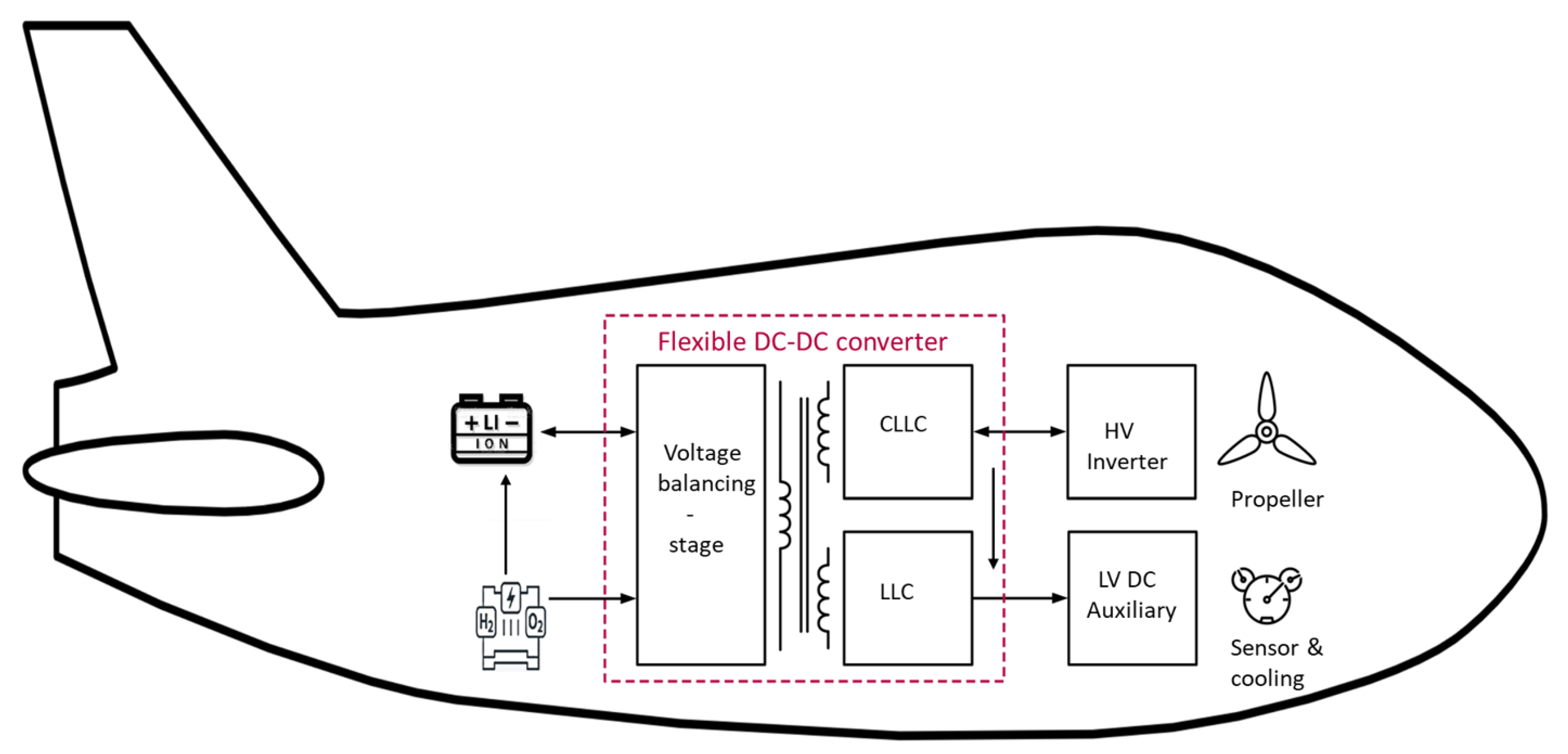
A Flexible DC–DC Converter with Multi-Directional Power Flow Capabilities for Power Management and Delivery Module in a Hybrid Electric Aircraft

 , ,
, ,
Abstract
:1. Introduction
2. Concept and Modes of Operation
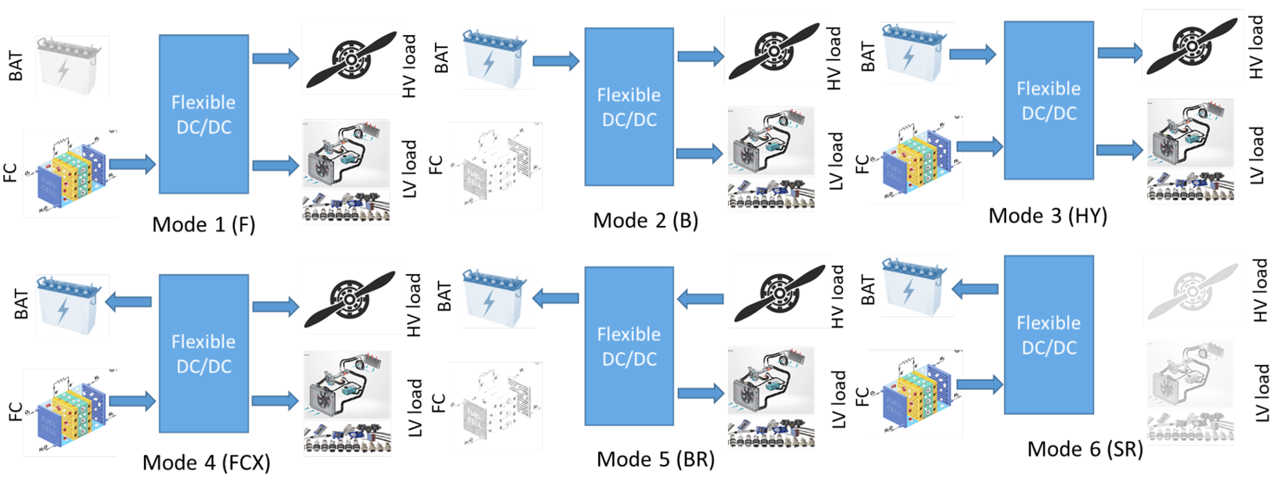
- Mode 1: Fuel cell to loads (F) The aircraft’s principal operation mode is the fuel cell mode. Only the fuel cell provides electricity to the motor and other loads throughout the en-route and holding stages. The fuel cell mode is used if the highest feasible fuel cell power is greater than or equal to the total load power demand. This mode is selected if the fuel cell power alone is sufficient to sustain the required motor power plus losses, and battery charging is not required.
- Mode 2: Battery to load (B) The battery module powers the entire aircraft loads in this mode. This mode is usually regarded as a backup safety mode, in case the fuel cell has a failure. The battery can be used as a redundant backup power source and provide sufficient power to perform an emergency landing. The battery must be sufficiently charged (i.e., high SOC) to use battery-only mode.
- Mode 3: Hybrid mode—Fuel cell and Battery to loads (HY) When the power demand of the loads exceeds the maximum fuel cell power, hybrid mode is used. Fuel cell and battery are simultaneously used to supply power to the loads in this mode. This mode is typically needed during the take-off and climb phase, where peak power demand is very high. At high load current, the voltage output drops significantly, and the fuel cell voltage can be higher or lower than the battery during operation. The voltage output of a Li-ion battery depends on the state of charge and the current but typically varies less than the fuel cell voltage. Hence, this mode necessitates a careful voltage balancing operation.
- Mode 4: Fuel cell to load and Battery Charging (FCX) This mode can be used during cruising or holding phase to recharge the battery during the course of the flight while simultaneously supplying energy to the loads. Similar to hybrid mode, a delicate voltage balancing is needed to match the load and battery voltage.
- Mode 5: Recuperation to Battery (BR) The DC bus voltage generated by the motor during recuperation can be utilized to charge the battery voltage if the battery is not already fully charged (SOC < 100%) while simultaneously supplying energy to the LV loads. This mode uses the braking energy generated by the propeller motor during descent or landing and charges the battery to regain some SOC. Recuperation increases the efficiency of the aircraft as the generated braking energy, instead of being wasted in form of heat in the brakes, is used for charging the batteries.
- Mode 6: Static Battery charging from fuel cell (SR) This mode is reserved for emergency operations and can only be performed when the aircraft is stationary and all loads are entirely powered off. A hypothetical example of usage is the aircraft has an emergency landing, and battery SOC is very low or depleted so that a new take-off is impossible. Using this mode, the fuel cell can charge the battery directly to gain some SOC in the battery.
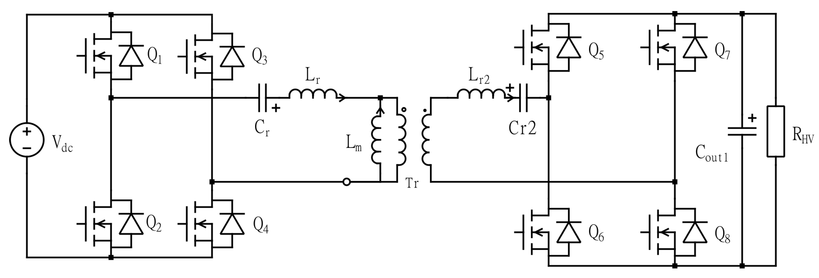
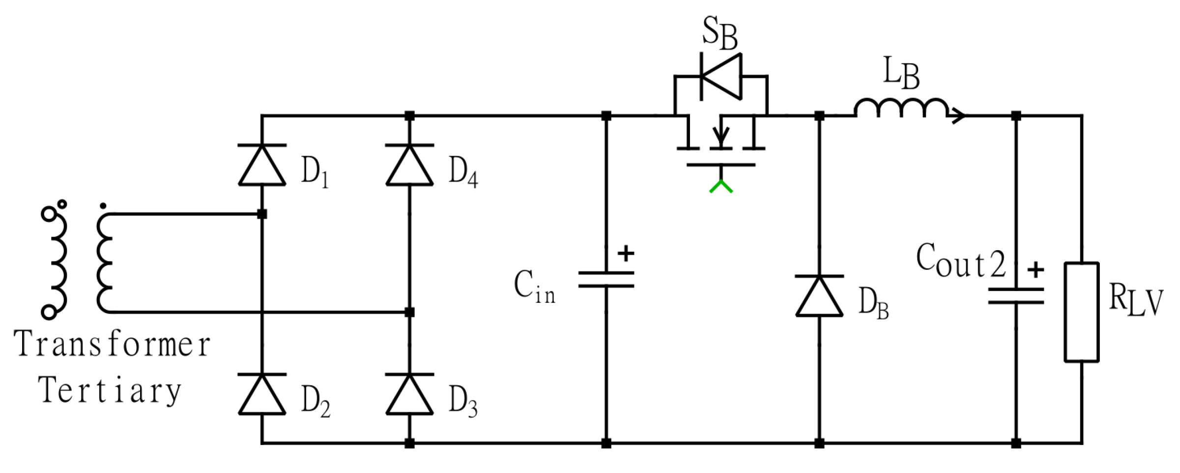
3. Proposed Converter Topology
3.1. Resonant Converter Stage
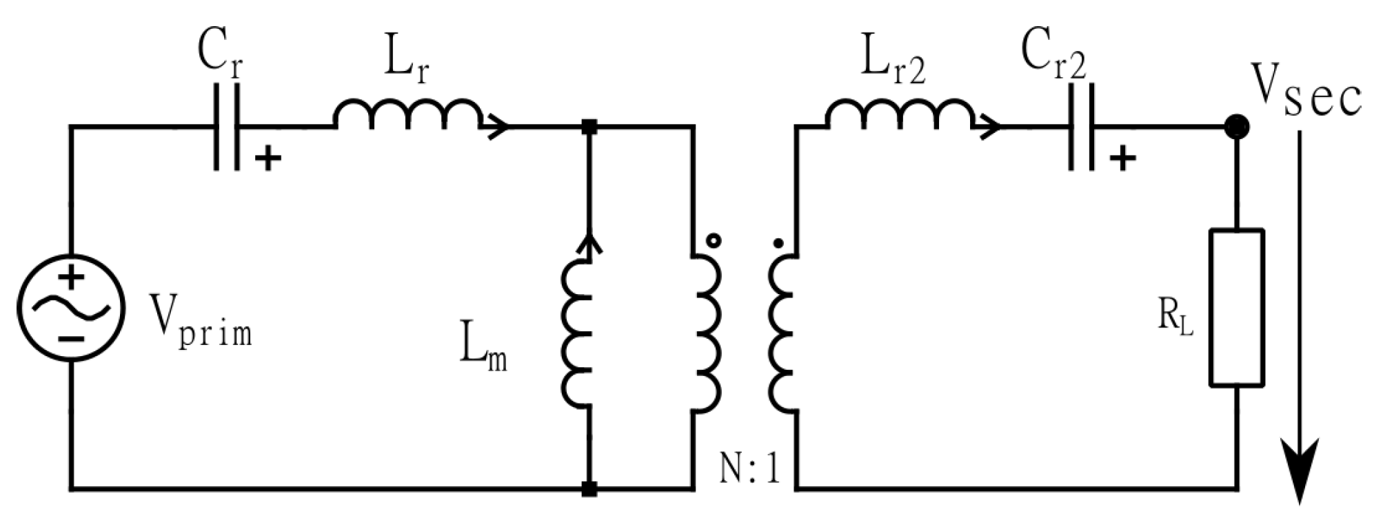
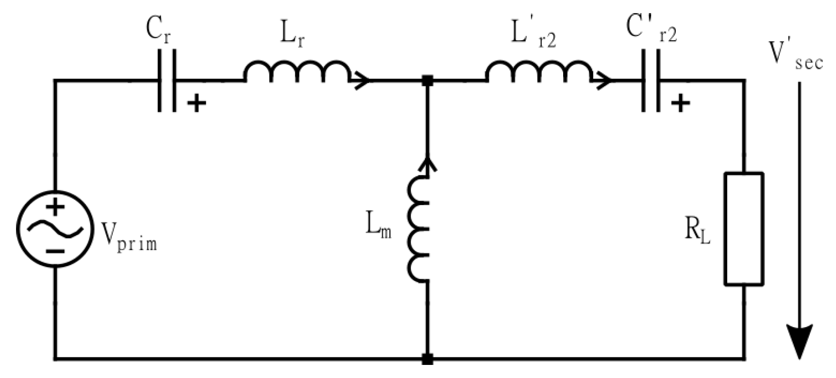
3.1.1. HV Output with CLLC Converter
Design Process
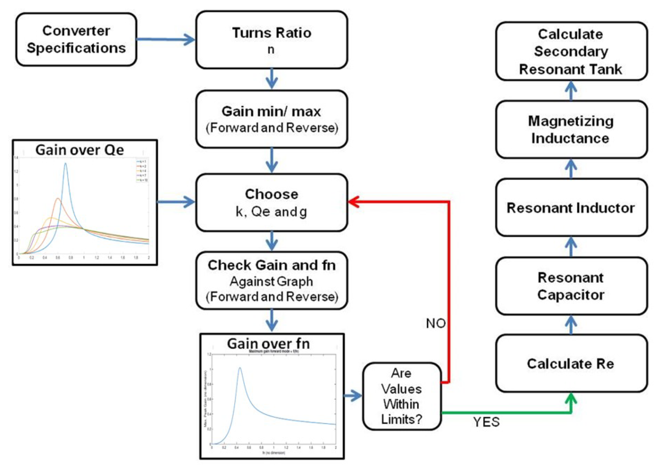
- The first step is to obtain the turns-ratio of the transformer. The turns ratio of the transformer depends on the nominal input voltage (Vin,nom) and the output voltage (Vout,mean). If the forward MOSFET voltage drop and the diode forward voltage drop are ignored, the turns ratio (N) can be obtained from Equation (11).
- Next, the maximum voltage gain (Mmax) and minimum voltage gain (Mmin) is to be decided. Since gain requirements change with the direction of power transfer, two separate gain formulas must be regarded. The voltage gain is the ratio of output voltage and input voltage and is not a fixed value if the converter’s input voltage fluctuates. These two parameters are calculated based on design constraints based in Equation (12):
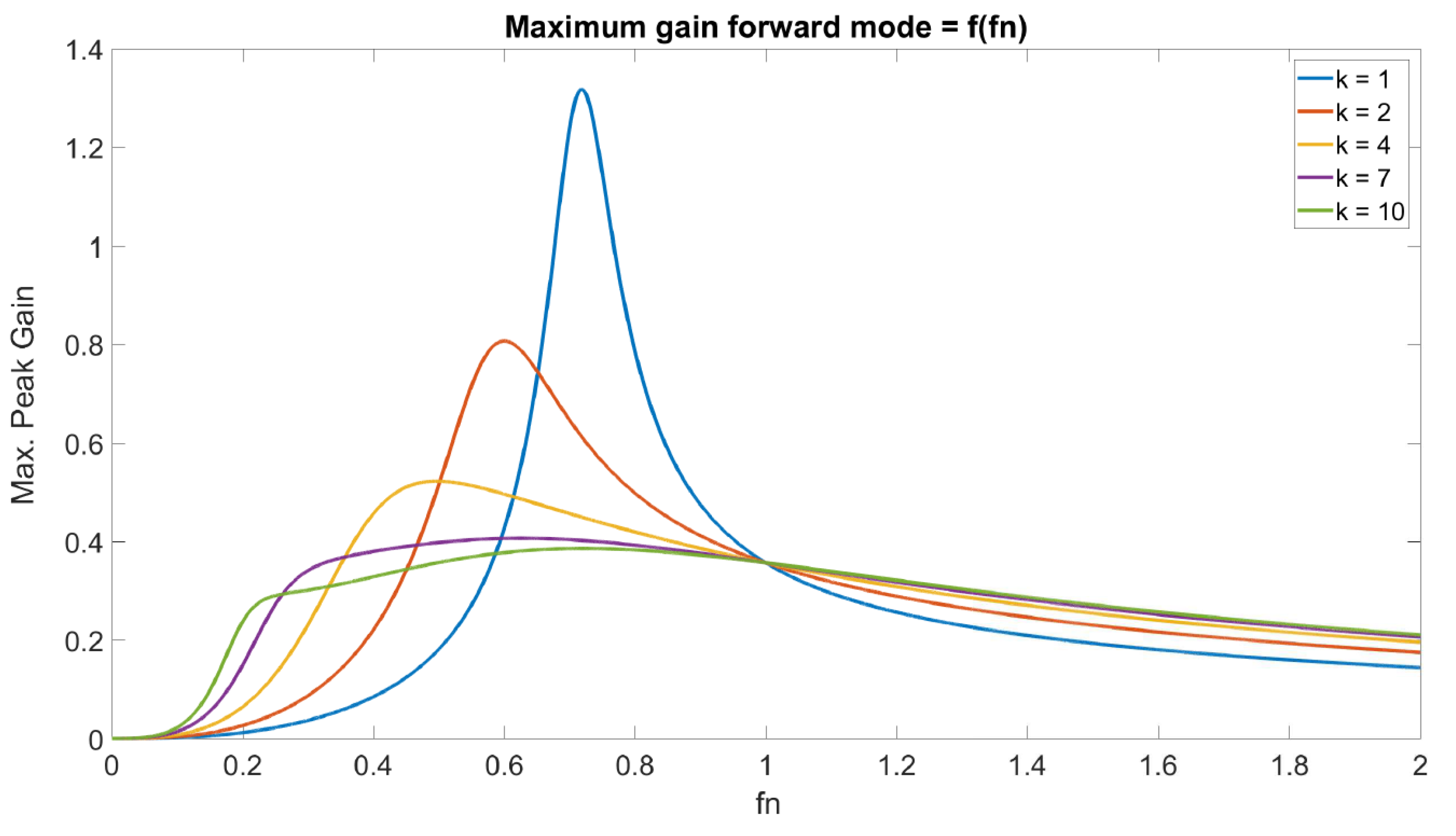
- The parameter k is another critical parameter for the design. It is demarcated by the ratio of the primary magnetization inductance () and the equivalent leakage inductance (). The inductance ratio (k) is an important parameter that helps in shaping the gain curve. A small k usually results in considerable magnetization losses inside the transformer. On the other hand, a higher inductance ratio causes a limited gain but offers a broader operating frequency range and enhances efficiency. Figure 9 exhibits the effect of converter gain (in the forward direction) due to variation of parameter k when and g are assumed constant. Since the focus of the converter is to optimize efficiency, a higher value of k is advised.Figure 9. Variation of the gain curve due to variation of parameter k over normalized switching frequency.Figure 9. Variation of the gain curve due to variation of parameter k over normalized switching frequency.
![Energies 15 05495 g009]()
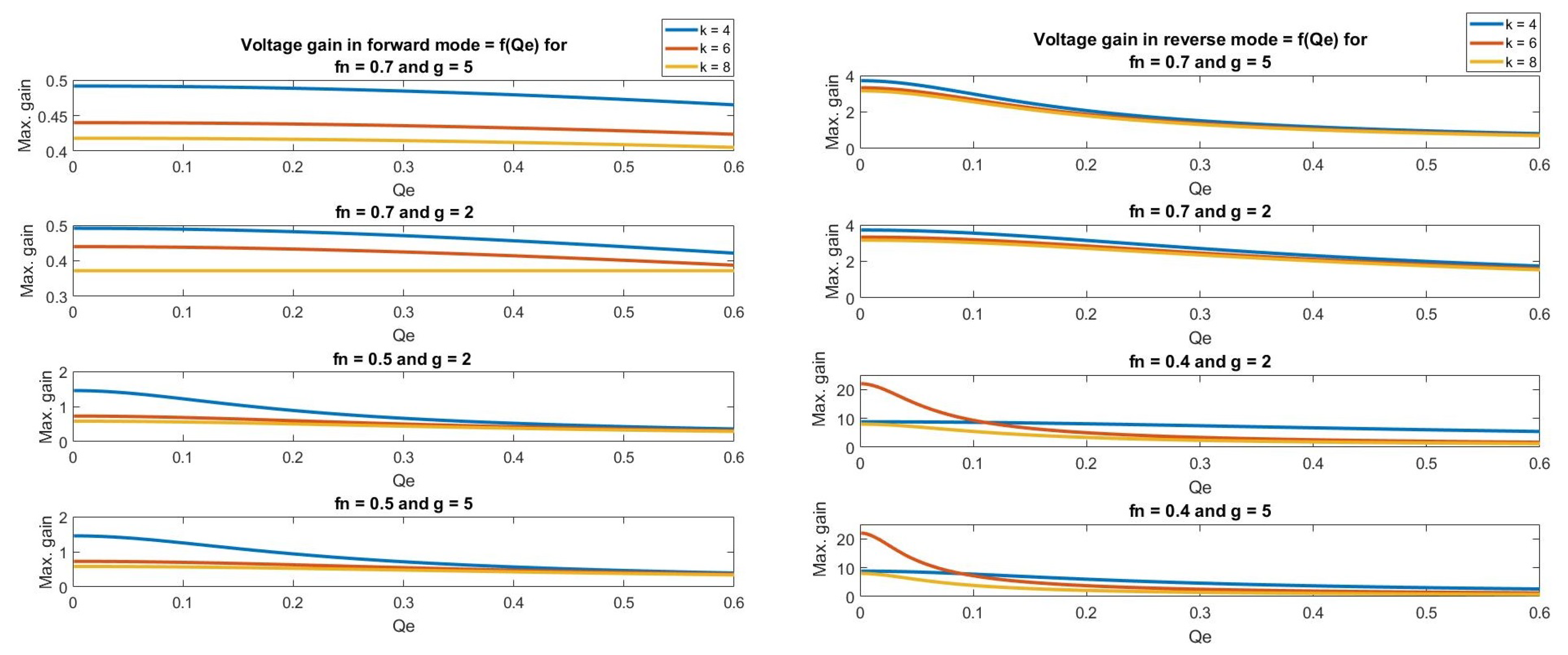
- Subsequently, the value of is obtained. In order to investigate the effect of on the gain curve, the gain curve is plotted for a fixed value of over variable values of K and g for both forward and reverse directions. The result of this analysis is shown in Figure 10. From these curves, the optimal value of is to be determined from the previously discussed gain requirements that guarantees the required gains conveyed in Equation (12).Figure 10. Gain curve for variable values of k and g in (left) forward direction, (right) reverse direction.Figure 10. Gain curve for variable values of k and g in (left) forward direction, (right) reverse direction.
![Energies 15 05495 g010]()
- Next, the value of g is to be determined. It can be observed in Figure 10 that the value of the capacity ratio g does not have a significant effect on the gain curve. Nevertheless, at higher frequencies and with a higher value of g, a higher quality factor can be selected since the gradient of the curve is steeper in the lower region. However, this effect is noticeably reduced at lower switching frequencies. It is advisable to keep the resonance frequencies of the primary and secondary sides in similar values according to the Equation (13), where, is the primary resonance inductance, is the secondary resonance inductance, is the primary resonance capacitance, and is the secondary resonance capacitance.Hence, the ratio of leakage inductance to the resonant capacitor is kept the same. However, if a large g is chosen, the inductance of the secondary side will have to be significantly reduced. Since, Lrs has a lower limit due to the leakage inductance of the transformer, this constricts the selection of g to a lower value.
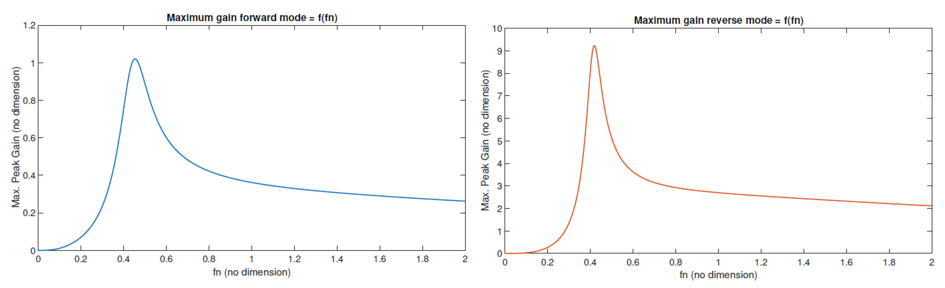
- Finally, forward and reverse gain curves are plotted with the selected values of , k, and g is to validate if the design meets the gain requirement (Figure 11). The resonant tank parameters are calculated using Equations (6)–(9). The overview of the iterative design process is shown in Figure 12.Figure 11. Forward and reverse gain from the selected values of , k, and g.
![Energies 15 05495 g011]() Figure 12. Iterative design flowchart of the CLLC converter design.
Figure 12. Iterative design flowchart of the CLLC converter design.![Energies 15 05495 g012]()
3.1.2. LV Output with LLC Converter and Integrated Buck Converter
3.2. The Voltage Balancing Stage
- the target DC–link voltage is higher than both battery and fuel cell
- battery voltage can be higher or lower than the fuel cell depending on the operation conditions.
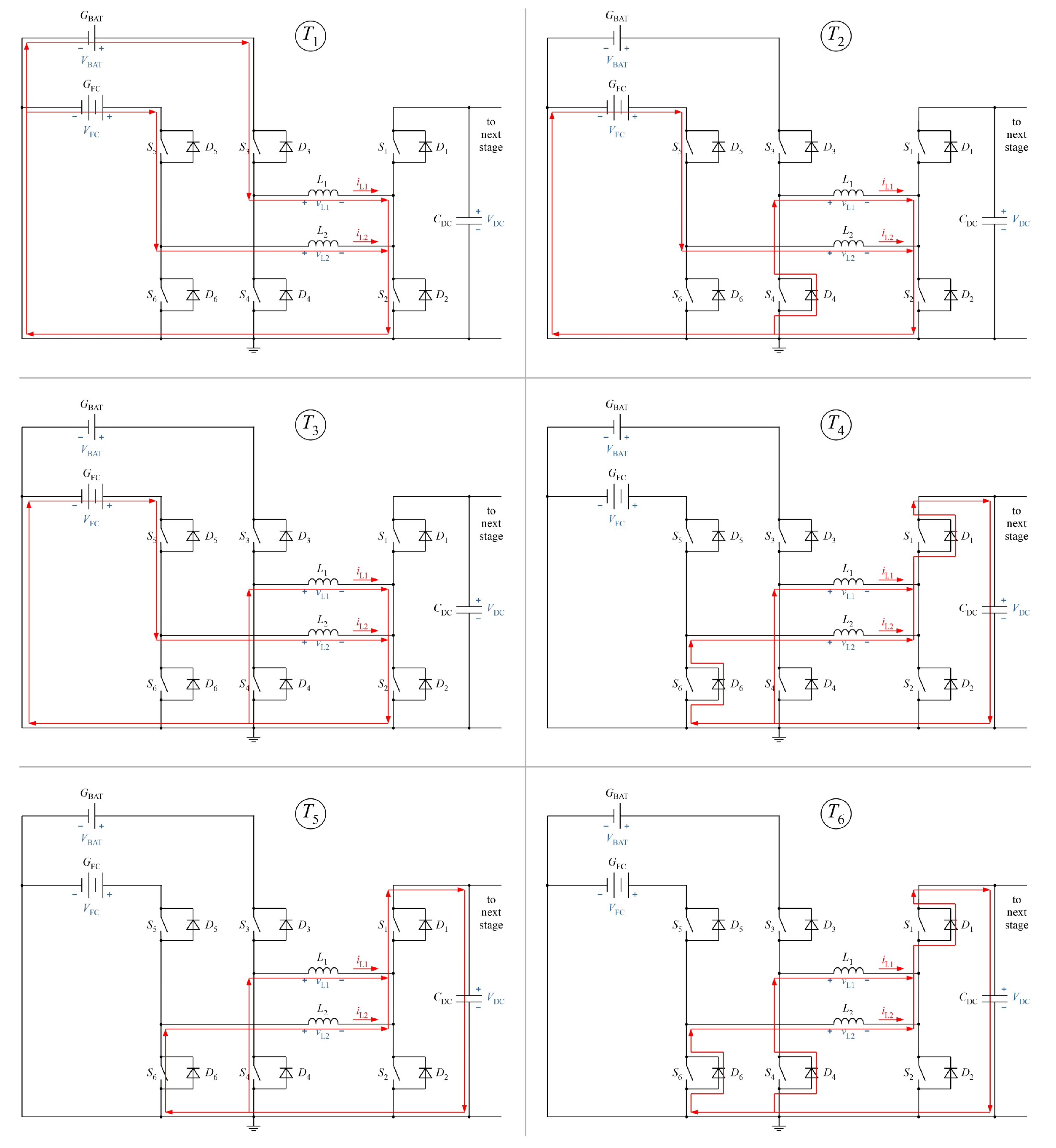
3.2.1. Battery to DC–Link Capacitor (B2DC) Mode
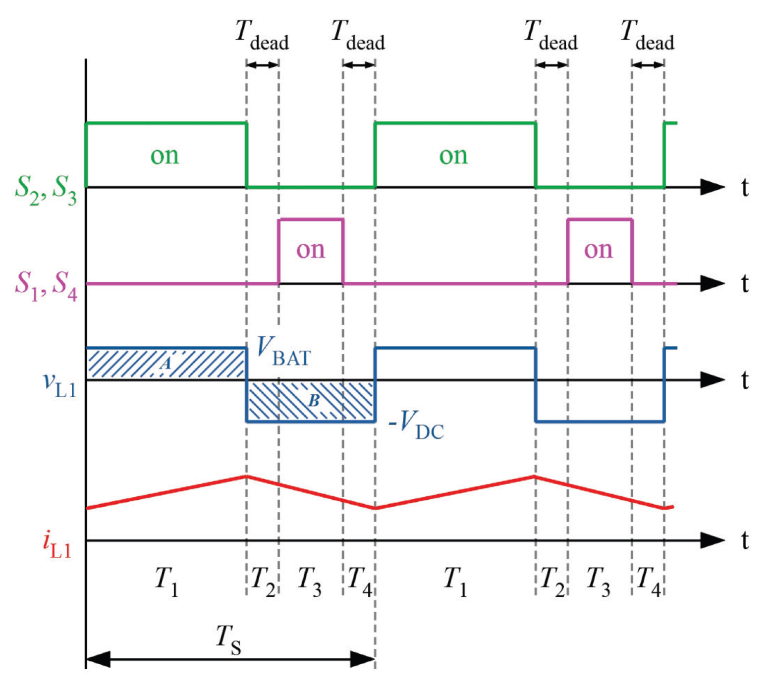
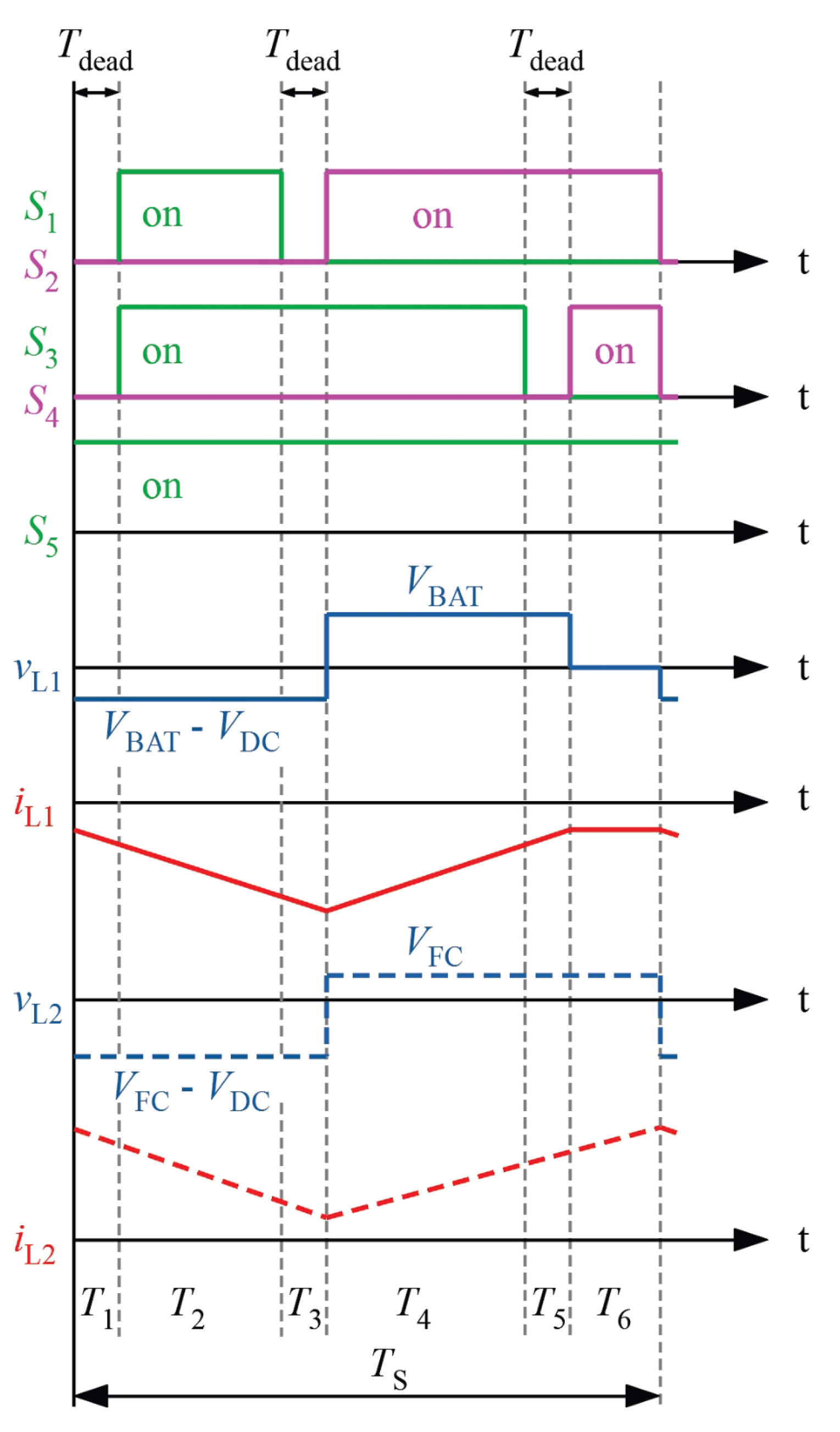
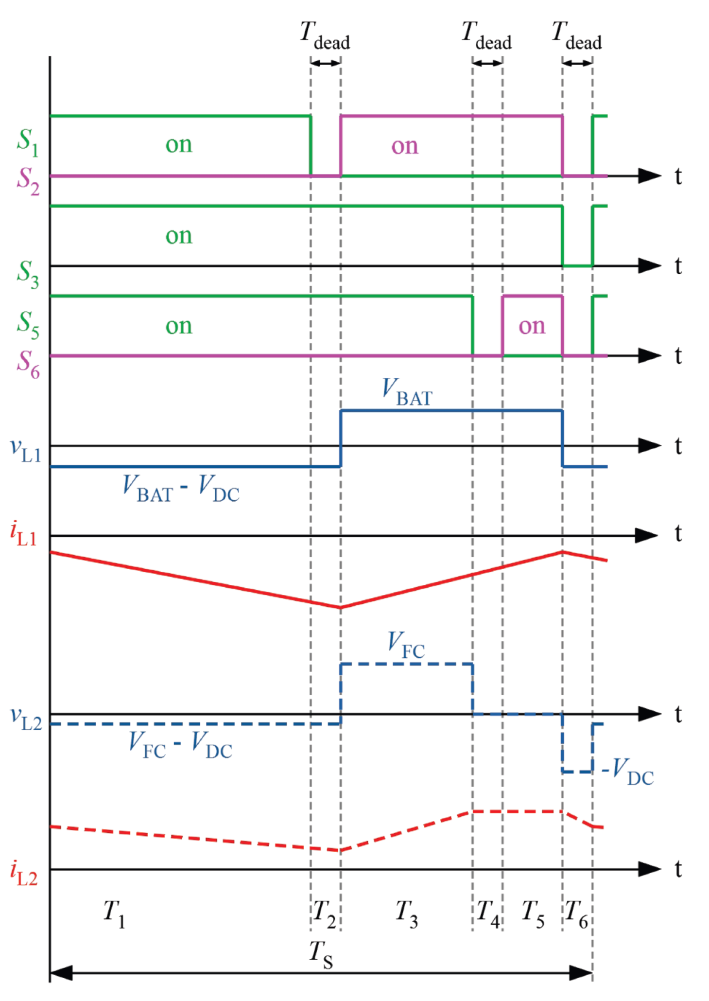
- During , the active switches and are both turned-on. In this time interval, inductor is directly charged from the battery, and the current increases through the inductor with a slew rate of /, and the current flowing through the rises linearly.
- Time interval is a dead time interval in which all switches are turned-off. As the switches and are no longer conducting, the inductor current iL1 is forced to commutate through the body diode of () and (). This facilities the zero voltage switching of and when turned-on during the next time window. The current through inductor falls at a rate of /.
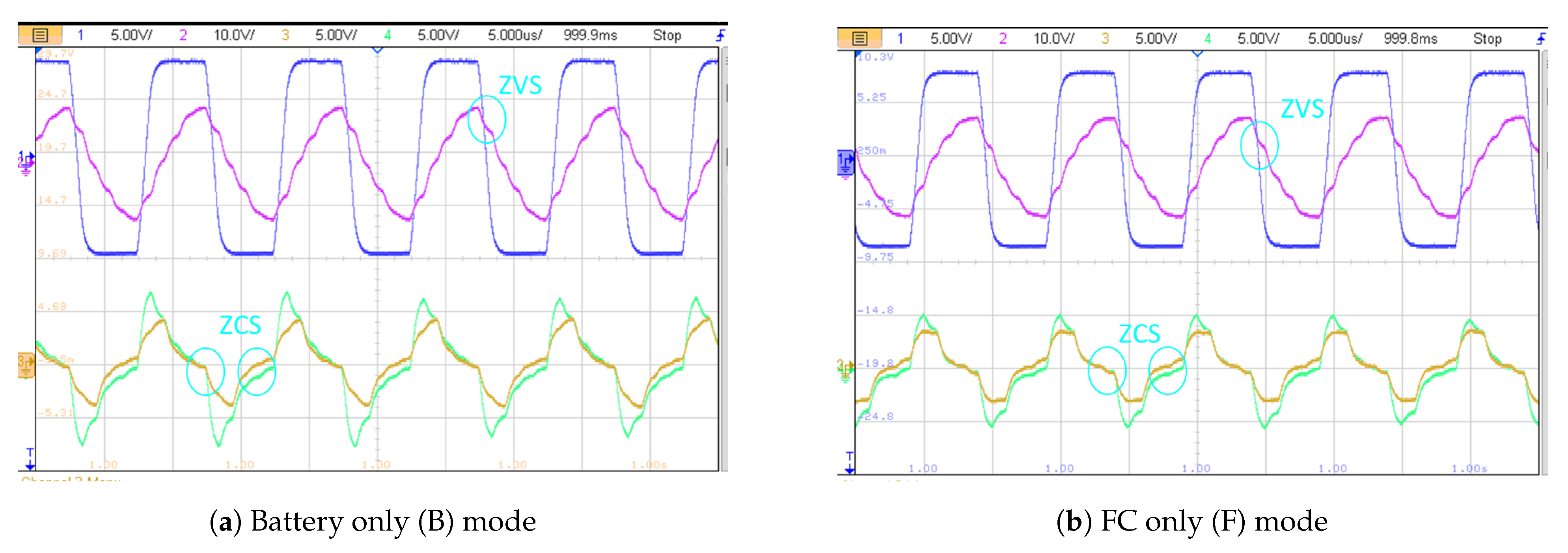
- During , the switch pair and are turned-on at ZVS, and conduction losses are minimized.
- During all switches are turned-off and the inductor current commutates back to body diodes and again. Afterward, the sequence is repeated. It is worth mentioning that during , and will be inevitably hard-switched. The switching states of the switches and the resulting inductor currents and voltages are shown in Figure 14.Figure 14. Active switch states, inductor voltage and inductor current for BAT and DC–link.
![Energies 15 05495 g014]()
3.2.2. Fuel Cell to DC–Link Capacitor (FC2DC) Mode
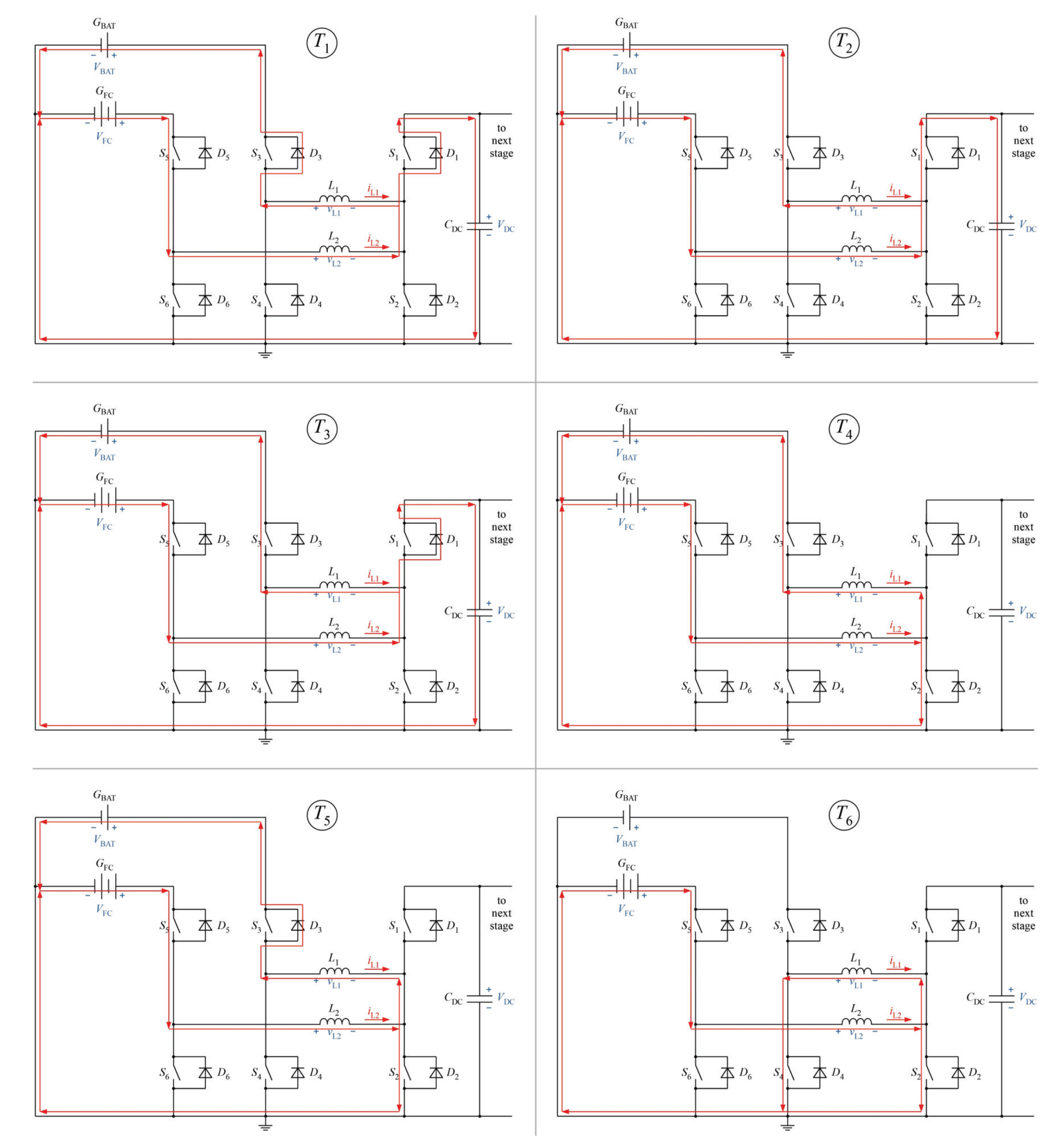
3.2.3. Battery and Fuel Cell to DC–Link Capacitor (BFC2DC) Mode
- Time interval : During this time interval, inductor and are actively charged. This is achieved by turning-on the switches , and . Inductor is charged from the battery and the is charged from the fuel cell and a magnetic field builds up inside these inductors. The current through them increases linearly by slew-rates of / and /, respectively. At the end of the time interval is completely charged.
- Time interval : At the beginning of this time interval is turned-off and as a result current automatically commutates through the body diode () of . This provides a free wheeling state for current through while keeps on getting charged from the fuel cell.
- Time interval : In this time interval, switch is turned-on and is switched on at ZVS, minimizing the switching and conduction losses at . At the end of , the inductor is also fully charged.
- Time interval : In this time interval is turned-off. As a result inductor current through commutates through the body diode of (). At the same time the body diode of () is forward biased and both inductors and start transferring energy to the DC–link capacitor.
- Time interval : Here, the switches and are both turned-on. The switch which was activated previously at also remains on in this time interval. As a result both switches are turned-on at ZVS and conduction losses are minimized. The energy from and is transferred to the DC–link and as a result the magnetic energy of these inductors falls at a slew-rate / and /, respectively.
- Time interval : This time interval serves as a mandatory dead time period where all switches are turned off and current is forced to flow through , and . Afterwards, switching pattern goes back to and the recharging of inductors starts again.
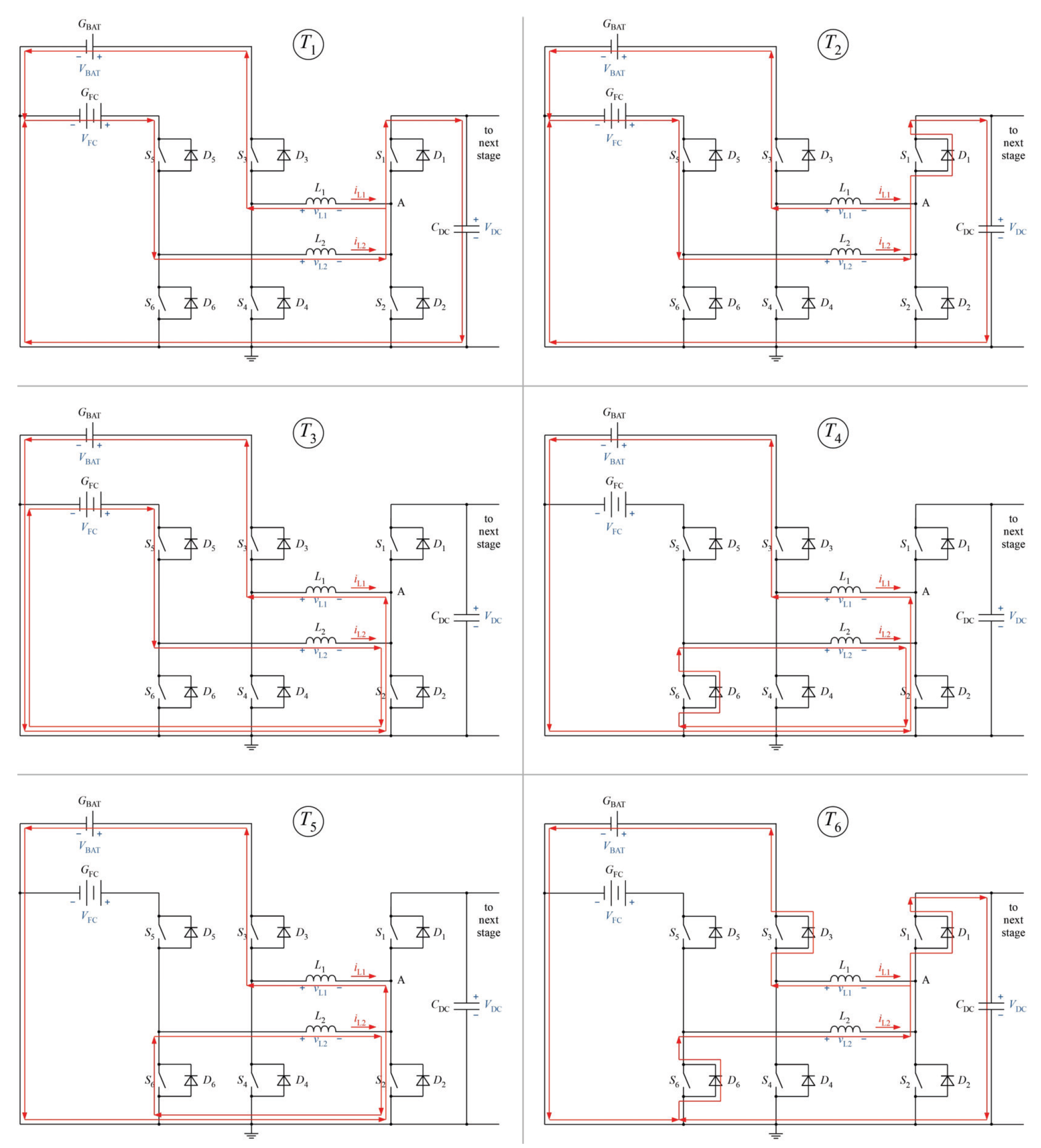
3.2.4. Fuel Cell to DC–Link and Battery Charging (FC2BDC) Mode
Fuel Cell Voltage Lower Than the Battery (Boost Mode)
- Time interval : During this interval only switch is turned-on. In this time interval the inductor discharges and charges both the battery and the DC–link. The body diode of () and the body diode of () are as a result forward biased.
- Time interval : During this interval switch and are also turned–on. Therefore, and are turned–on at ZVS and conduction losses are minimized. In this time-interval, the current from continues to charge both the battery and the DC–link.
- Time interval : During this interval is switched off. As a result, current transitions back to the body diode and provides necessary time to completely turn-off .
- Time interval : During this interval switch is turned-on and current is forced to commutate through switch to ground. In this interval the inductor charges the battery from the magnetic energy stored inside and is charged from the fuel cell.
- Time interval : Switch is turned-off and current to the battery is forced to commutate to the body diode of (). In this interval is charged from the fuel cell and continues to charge the battery.
- Time interval : Finally, and are turned-on providing a free-wheeling path for the inductor current . At the end of this time-period, is completely charged and switching-sequence is repeated.
Fuel Cell Voltage Is Higher Than the Battery (Buck–Boost Mode)
3.2.5. DC–Link Capacitor to Battery (DC2B) Mode
3.2.6. Fuel Cell to Battery Charge (FC2B) Mode
Buck-Mode
Boost-Mode
4. Experimental Setup and Results
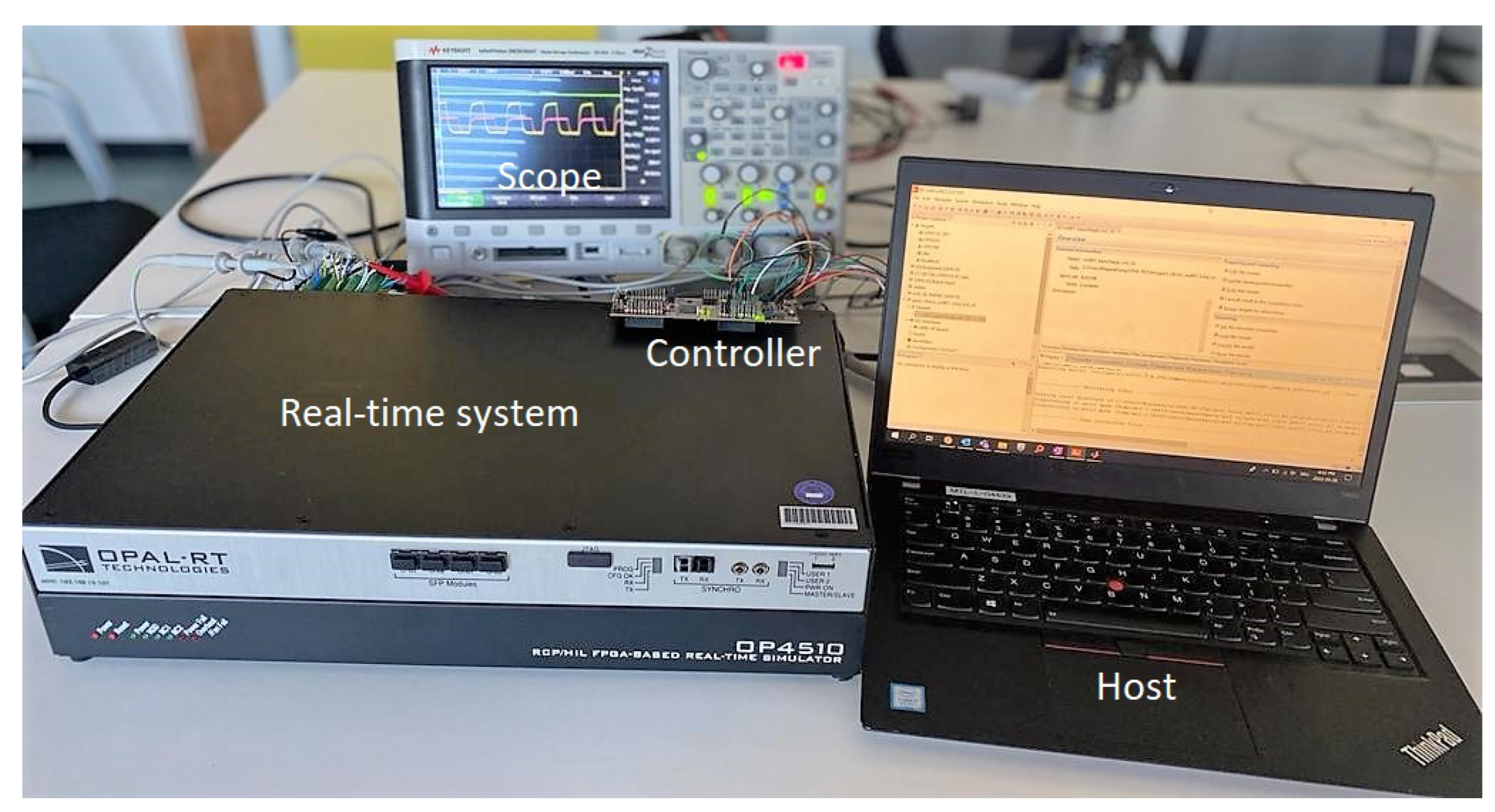
4.1. Experimental Setup
4.2. Experimental Results
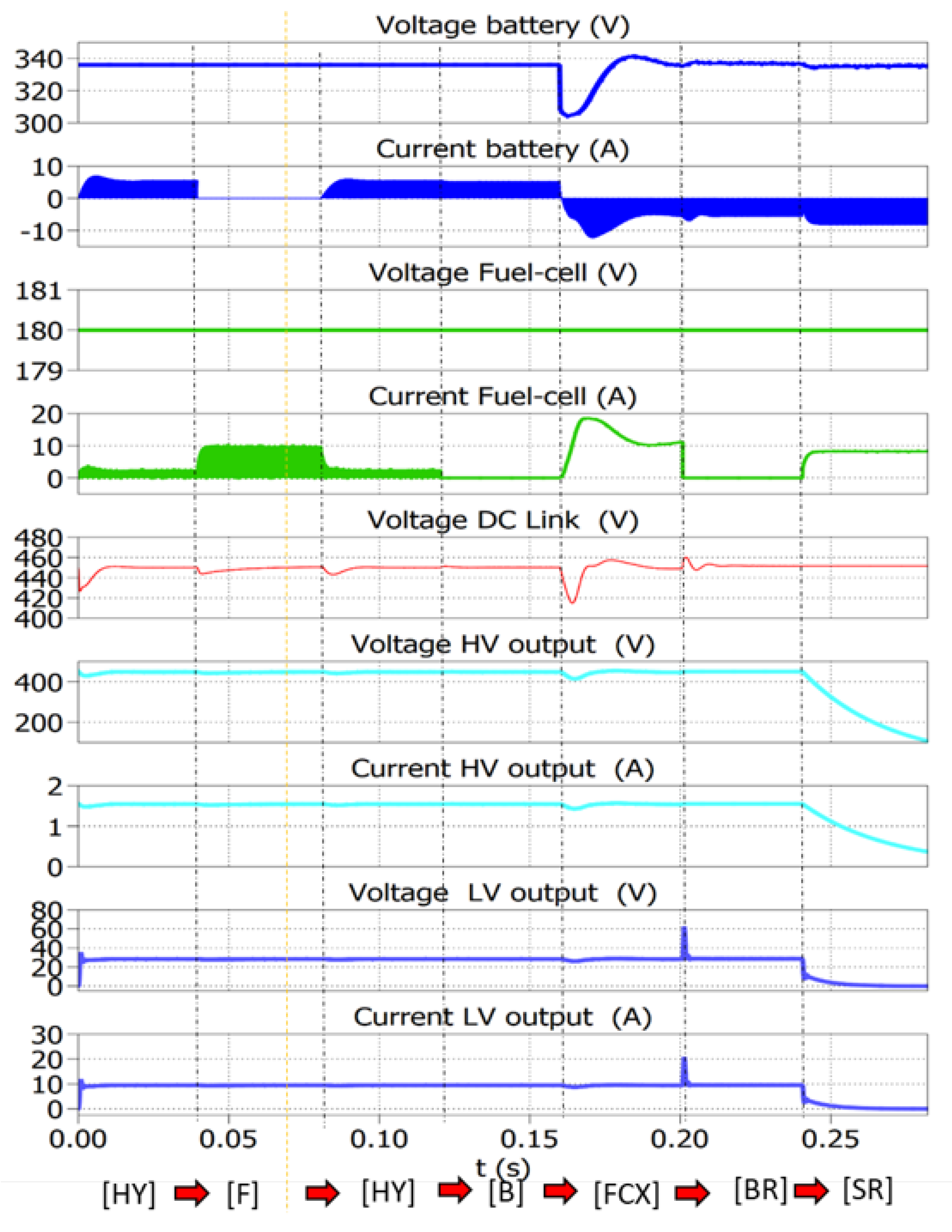
4.3. Mode Transitions
- a.
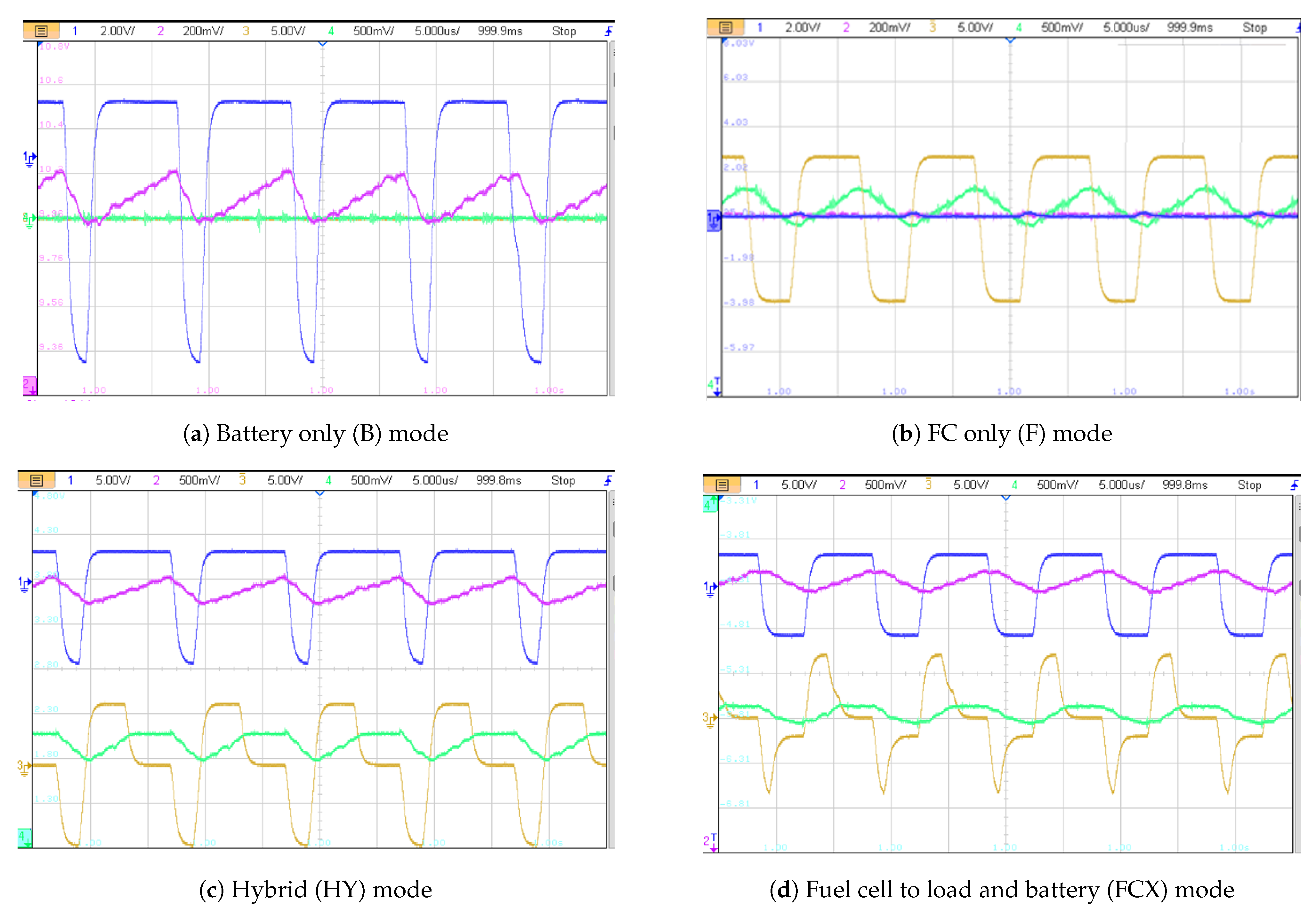
- During HY: Current is drawn from both battery and fuel cell. 450 V is obtained at the DC–link and 450 V is obtained at the HV DC output (750 W) while 28 V is obtained at the LV DC output (250 W).
- b.
- During F: Current is drawn from fuel cell only, and the battery is completely decoupled. 450 V is obtained at the DC–link and 450 V is obtained at the HV DC output (750 W), and 28 V is obtained at LV DC output (250 W).
- c.
- During HY: Same behaviour as in point a.
- d.
- During B: Current is drawn only from the battery and the fuel cell is completely decoupled. 450 V is obtained at the DC–link and 450 V is obtained at the HV DC output (750 W) while 28 V is obtained at LV DC output (250 W).
- e.
- During FCX: Current is drawn from fuel cell only and the battery is charged (negative current). 450 V is obtained at the DC–link and 450 V is obtained at the HV DC output (750 W) while 28 V is obtained at the LV DC output (250 W).
- f.
- During BR: Current is supplied from the HV DC output of 450 V, and the battery is charged from it (negative current). FC is completely decoupled as it does not support negative current. 450 V is obtained at the DC–link and 28 V is obtained at the LV DC output (250 W).
- g.
- During SR: Current is drawn from the fuel cell only and the battery is charged from it (negative current). No output voltage is obtained on the HV, and LV outputs as this mode is designed for stationary charging.
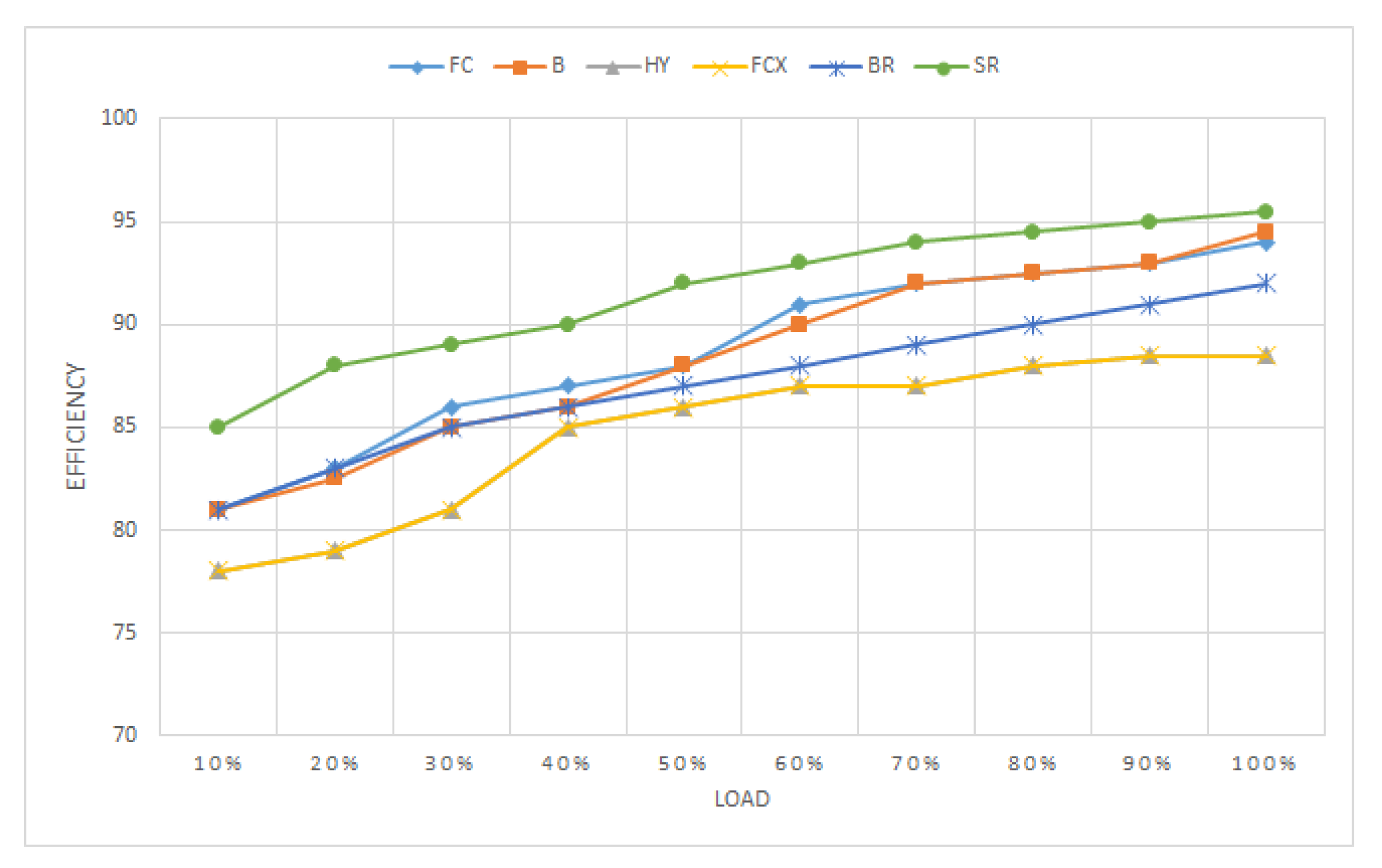
4.4. Efficiency
5. Comparison
6. Conclusions
Author Contributions
Funding
Institutional Review Board Statement
Informed Consent Statement
Data Availability Statement
Acknowledgments
Conflicts of Interest
Abbreviations
| BAT | Battery |
| DC | Direct current |
| DAB | Dual-active bridge |
| FC | Fuel cell |
| HiL | Hardware-in-the-loop |
| HV | High voltage |
| LV | Low voltage |
| OCV | Open circuit voltage |
| RT | Real time |
| SOC | State of charge |
References
- Erbach, G. Briefing EU Legislation in Progress: CO2 Emissions from Aviation. 2017. Available online: https://www.europarl.europa.eu/ (accessed on 1 April 2022).
- Engel, S.P.; Stieneker, M.; Soltau, N.; Rabiee, S.; Stagge, H.; de Doncker, R.W. Comparison of the modular multilevel DC converter and the dual-active bridge converter for power conversion in HVDC and MVDC grids. IEEE Trans. Power Electron. 2015, 30, 124–137. [Google Scholar] [CrossRef]
- Nadal, M.; Barbir, F. Development of a hybrid fuel cell/battery powered electric vehicle. Int. J. Hydrogen Energy 1996, 21, 497–505. [Google Scholar] [CrossRef]
- Hoenicke, P.; Ghosh, D.; Muhandes, A.; Bhattacharya, S.; Bauer, C.; Kallo, J.; Willich, C. Power management control and delivery module for a hybrid electric aircraft using fuel cell and battery. Energy Convers. Manag. 2021, 244, 114445. [Google Scholar] [CrossRef]
- Ni, K.; Liu, Y.; Mei, Z.; Wu, T.; Hu, Y.; Wen, H.; Wang, Y. Electrical and Electronic Technologies in More-Electric Aircraft: A Review. IEEE Access 2019, 7, 76145–76166. [Google Scholar] [CrossRef]
- Balaji, C.; Dash, S.S.; Hari, N.; Babu, P.C. A four port non-isolated multi input single output DC–DC converter fed induction motor. In Proceedings of the 2017 IEEE 6th International Conference on Renewable Energy Research and Applications (ICRERA), San Diego, CA, USA, 5–8 November 2017; pp. 631–637. [Google Scholar] [CrossRef]
- Savitha, K.P.; Kanakasabapathy, P. Multi-port DC–DC converter for DC microgrid applications. In Proceedings of the 2016 IEEE 6th International Conference on Power Systems (ICPS), New Delhi, India, 4–6 March 2016; pp. 1–6. [Google Scholar] [CrossRef]
- Muralikrishnan, N.; Madhanakkumar, N.; Bharani, S.R.N.S. Multi-Port DC–DC Converter for Renewable Resources. In Proceedings of the 2021 International Conference on System, Computation, Automation and Networking (ICSCAN), Puducherry, India, 30–31 July 2021; pp. 1–3. [Google Scholar] [CrossRef]
- Hintz, A.; Prasanna, U.R.; Rajashekara, K. Novel Modular Multiple-Input Bidirectional DC–DC Power Converter (MIPC) for HEV/FCV Application. IEEE Trans. Ind. Electron. 2015, 62, 3163–3172. [Google Scholar] [CrossRef]
- Buticchi, G.; Costa, L.F.; Barater, D.; Liserre, M.; Amarillo, E.D. A Quadruple Active Bridge Converter for the Storage Integration on the More Electric Aircraft. IEEE Trans. Ind. Electron. 2018, 33, 8174–8186. [Google Scholar] [CrossRef] [Green Version]
- Gu, C.; Yan, H.; Yang, J.; Sala, G.; De Gaetano, D.; Wang, X.; Galassini, A.; Degano, M.; Zhang, X.; Buticchi, G. A Multiport Power Conversion System for the More Electric Aircraft. IEEE Trans. Transp. Electrif. 2020, 6, 1707–1720. [Google Scholar] [CrossRef]
- Bhattacharya, S.; Willich, C.; Hoenicke, P.; Kallo, J. A Novel Re-configurable LLC Converter for Electric Aircraft. In Proceedings of the 2021 IEEE 12th Energy Conversion Congress and Exposition—Asia (ECCE-Asia), Singapore, 24–27 May 2021; pp. 32–37. [Google Scholar] [CrossRef]
- Khodabakhsh, J.; Moschopoulos, G. A Multiport Converter for More Electric Aircraft with Hybrid AC-DC Electric Power System. In Proceedings of the 2021 IEEE Energy Conversion Congress and Exposition (ECCE), Vancouver, BC, Canada, 10–14 October 2021; pp. 1876–1881. [Google Scholar] [CrossRef]
- Ivey, C.; Alfares, A.; He, J. Hybrid-Electric Aircraft Propulsion Drive Based on SiC Triple Active Bridge Converter. In Proceedings of the 2021 IEEE/IAS Industrial and Commercial Power System Asia (I and CPS Asia), Chengdu, China, 18–21 July 2021; pp. 431–436. [Google Scholar] [CrossRef]
- Rahrovi, B.; Mehrjardi, R.T.; Ehsani, M. On the Analysis and Design of High-Frequency Transformers for Dual and Triple Active Bridge Converters in More Electric Aircraft. In Proceedings of the 2021 IEEE Texas Power and Energy Conference (TPEC), College Station, TX, USA, 2–5 February 2021; pp. 1–6. [Google Scholar] [CrossRef]
- Zhang, J.; Chen, T.; Zhong, S.; Wang, J.; Zhang, W.; Zuo, X.; Maunder, R.G.; Hanzo, L. Aeronautical AdHoc Networking for the Internet-Above-the-Clouds. Proc. IEEE 2019, 107, 868–911. [Google Scholar] [CrossRef] [Green Version]
- Zhao, S. High Frequency Isolated Power Conversion from Medium Voltage AC to Low Voltage DC. Master’s Thesis, VTechWorks. Virginia Polytechnic Institute and State University, Blacksburg, VA, USA, 2017. [Google Scholar]
- Bhattacharya, S.; Willich, C.; Kallo, J. Design and Demonstration of a 540 V/28 V SiC-Based Resonant DC–DC Converter for Auxiliary Power Supply in More Electric Aircraft. Electronics 2022, 11, 1382. [Google Scholar] [CrossRef]
- Chang, H.-T.; Liang, T.-J.; Yang, W.-C. Design and Implementation of Bidirectional DC–DC CLLLC Resonant Converter. In Proceedings of the 2018 IEEE Energy Conversion Congress and Exposition (ECCE), Portland, OR, USA, 23–27 September 2018; pp. 2712–2719. [Google Scholar]
- Lin, F.; Zhang, X.; Li, X. Design Methodology for Symmetric CLLC Resonant DC Transformer Considering Voltage Conversion Ratio, System Stability, and Efficiency. IEEE Trans. Power Electron. 2021, 36, 10157–10170. [Google Scholar] [CrossRef]
- Dong, Z.; Gregoire, L.A.; Vipin, V.N.; Chakraborty, S.; Sun, A.; Vetrivelan, A.; Feng, X.; Huang, A.Q. Real-time Implementation of a Dual-Active-Bridge Based Multi-Level Photovoltaic Converter. In Proceedings of the 2021 IEEE 12th International Symposium on Power Electronics for Distributed Generation Systems (PEDG), Chicago, IL, USA, 28 June–1 July 2021; pp. 1–6. [Google Scholar]
- Bhattacharya, S.; Grégoire, L.; Kallo, J.; Stevic, M.; Garg, M.; Willich, C. FPGA-based Real-Time Simulation for LLC Resonant Converter Prototyping. In Proceedings of the 2022 IEEE 13th International Symposium on Power Electronics for Distributed Generation Systems (PEDG 2022), Kiel, Germany, 26–29 June 2022. [Google Scholar]
- OPAL RT Technologies. Available online: https://www.opal-rt.com/solver-ehs-2/ (accessed on 5 April 2022).
- Harchegani, A.T.; Asghari, A.; Jazaeri, M. A new soft switching multi-input quasi-Z-source converter for hybrid sources systems. IET Renew. Power Gener. 2021, 15, 1451–1468. [Google Scholar] [CrossRef]
- Ning, J.; Zeng, J.; Du, X. A Four-port Bidirectional DC–DC Converter for Renewable Energy-Battery-DC Microgrid System. In Proceedings of the 2019 IEEE Energy Conversion Congress and Exposition (ECCE), Baltimore, MD, USA, 29 September–3 October 2019; pp. 6722–6727. [Google Scholar] [CrossRef]
- Faraji, R.; Ding, L.; Rahimi, T.; Farzanehfard, H.; Hafezi, H.; Maghsoudi, M. Efficient Multi-Port Bidirectional Converter With Soft-Switching Capability for Electric Vehicle Applications. IEEE Access 2021, 9, 107079–107094. [Google Scholar] [CrossRef]
- Faraji, R.; Farzanehfard, H.; Esteki, M.; Khajehoddin, S.A. A Lossless Passive Snubber Circuit for Three-Port DC–DC Converter. IEEE J. Emerg. Sel. Top. Power Electron. 2021, 9, 1905–1914. [Google Scholar] [CrossRef]
- Honarjoo, B.; Madani, S.M.; Niroomand, M.; Adib, E. Non-isolated high step-up three-port converter with single magnetic element for photovoltaic systems. IET Power Electron. 2018, 11, 2151–2160. [Google Scholar] [CrossRef]


| Boost mode | , | , | , | , |
| Boost mode | , | , | , | , |
| , , | , , | , , | , , | , , | , , |
| , , | , , | , , | , , | , , | , , |
| , , | , , | , , | , , | , , | , , |
| , | , | , | , |
| Mode | ||||
|---|---|---|---|---|
| Buck-mode | , | , | , | , |
| Boost-mode | , | , | , | , |
| Description | Parameter | Value |
|---|---|---|
| Design Requirement | Battery Voltage | 300–336 V |
| Fuel cell Voltage | 180–400 V | |
| HV output voltage (power) | 450V (750 W) | |
| LV output voltage (power) | 28 V (250 W) | |
| DC–link target voltage | 450 V ± 5% | |
| Voltage-balancing stage | Inductor | 4 mH |
| Inductor | 3 mH | |
| Switching frequency | 100 kHz | |
| 100 F | ||
| Resonant converter stage | 50 nH | |
| 15 H | ||
| 200 H | ||
| Transformer turn-ratio | 80:29:09 | |
| 30 H | ||
| 400 H | ||
| Switching frequency | 80–250 kHz |
| Switch | CLLC Primary | CLLC Secondary | |||||||
|---|---|---|---|---|---|---|---|---|---|
| Mode | Duty | Duty | Duty | Duty | Duty | Duty | Duty | Sw. Frequency | Sw. Frequency |
| B | 40.6% | 59.4% | 59.4% | 40.6% | - | - | 20% | 175 kHz | - |
| F | 20.8% | 79.2% | - | - | 79.2% | 20.8% | 20% | 175 kHz | - |
| HY | 27% | 73% | 38% | 62% | 73% | 27% | 20% | 175 kHz | - |
| FCX | 39% | 61% | 51% | 49% | 100% | 0% | 20% | 175 kHz | - |
| BR | 45% | 55% | 55% | 45% | - | - | 47% | - | 87.2 kHz |
| SR | - | - | 36.3% | 63.7% | 100% | - | - | - | - |
Publisher’s Note: MDPI stays neutral with regard to jurisdictional claims in published maps and institutional affiliations. |
© 2022 by the authors. Licensee MDPI, Basel, Switzerland. This article is an open access article distributed under the terms and conditions of the Creative Commons Attribution (CC BY) license (https://creativecommons.org/licenses/by/4.0/).
Share and Cite
Bhattacharya, S.; Anagnostou, D.; Schwane, P.; Bauer, C.; Kallo, J.; Willich, C. A Flexible DC–DC Converter with Multi-Directional Power Flow Capabilities for Power Management and Delivery Module in a Hybrid Electric Aircraft. Energies 2022, 15, 5495. https://doi.org/10.3390/en15155495
Bhattacharya S, Anagnostou D, Schwane P, Bauer C, Kallo J, Willich C. A Flexible DC–DC Converter with Multi-Directional Power Flow Capabilities for Power Management and Delivery Module in a Hybrid Electric Aircraft. Energies. 2022; 15(15):5495. https://doi.org/10.3390/en15155495
Chicago/Turabian StyleBhattacharya, Sumantra, Dimosthenis Anagnostou, Patrick Schwane, Christiane Bauer, Josef Kallo, and Caroline Willich. 2022. "A Flexible DC–DC Converter with Multi-Directional Power Flow Capabilities for Power Management and Delivery Module in a Hybrid Electric Aircraft" Energies 15, no. 15: 5495. https://doi.org/10.3390/en15155495
APA StyleBhattacharya, S., Anagnostou, D., Schwane, P., Bauer, C., Kallo, J., & Willich, C. (2022). A Flexible DC–DC Converter with Multi-Directional Power Flow Capabilities for Power Management and Delivery Module in a Hybrid Electric Aircraft. Energies, 15(15), 5495. https://doi.org/10.3390/en15155495