Article

Practical Evaluation of Loss Reduction in Isolated Series Resonant Converter with Fixed Frequency Modulation

1
College of Electrical Engineering, Zhejiang University, Hangzhou 310027, China
2
College of Energy and Electrical Engineering, Hohai University, Nanjing 211100, China
3
Institute of Forestry and Engineering, Estonian University of Life Sciences, 51006 Tartu, Estonia
*
Author to whom correspondence should be addressed.
Energies 2022, 15(16), 5802; https://doi.org/10.3390/en15165802
Submission received: 8 July 2022 / Revised: 3 August 2022 / Accepted: 9 August 2022 / Published: 10 August 2022

Abstract

:
Nowadays, power converters with reduced cost, compact size and high efficiency are evolving to overcome the emergent challenges of renewable energy integrations. In this context, there is an increased demand for well-designed power converters in renewable energy applications to reduce energy utilization and handle a variety of loads. This paper proposes a center-tapped bridge cascaded series-resonant LC dual active bridge (DAB) converter for DC-DC conversion. The low part count of the proposed converter enables a high-power density design with reduced cost. The proposed converter offers reduced conduction losses as the reverse current is eliminated by adopting current blocking characteristics. Reverse current blocking also enables zero voltage switching (ZVS) and zero current switching (ZCS) over a wide operating range. Therefore, using a simple fixed frequency modulation (FFM) scheme offers a wide operating range compared to a conventional DAB converter. A thorough comparison of the proposed converter and a conventional DAB converter is provided based on conduction losses and switching losses to illustrate the performance improvement. Lastly, the effectiveness of the proposed converter is validated through simulation and experimental results.

1. Introduction

Demand for electric power keeps on increasing nowadays. Therefore, the world is switching over to the field of renewable energy sources as it is pollution free, free of cost, and easy to access in remote areas [1,2]. Researchers are mainly focusing on solar PV generation renewable energy sources since it is more reliable and easier to install. The output voltage of a photovoltaic system is variable due to the uncertainty of environmental conditions. However, to provide a constant and regulated output voltage, power electronic DC-DC converters are employed [3,4,5]. A dual-active-bridge (DAB) DC-DC converter was initially proposed in [6]. It has gained increasing attention for its use in high-power applications such as energy storage systems, electric vehicles, and solid-state transformers [7]. Due to the recent advancements in semiconductor devices, digital signal processors, and magnetic components, DAB converters have shown many advantages over their counterpart topologies (i.e., buck and boost converters) in terms of galvanic isolation, soft-switching capability, bidirectional power transfer, ease of control, high power conversion efficiency and high-power density [8,9,10,11].
DC-DC converters are classified into two types: isolated DC-DC converters and non-isolated DC-DC converters. In an isolated DC-DC converter, the input and output of the converter are isolated by an electrical barrier using a high-frequency transformer. The main advantage of the isolated DC-DC converter is that it protects the sensitive load from source disturbances, the output of the converter can be configured in either positive or negative polarity, and it has a high noise interference elimination capability. Numbers of isolated DC-DC converters are presented in the literature. Different DC-DC converter topologies are developed concerning higher efficiencies, reliable control switching strategies, fault-tolerant configurations, and mostly on renewable energy-based applications [12,13].
A conventional DAB converter is made up of two H-bridges connected via a high-frequency transformer (HFT). In contrast to the DC-DC topologies with unidirectional switches, the DAB topology employs current bidirectional switches that enable bidirectional power flow [14]. Inspired by DAB performance, DAB-based novel topologies are being investigated with the aim of improving performance with a reduced number of devices [6]. Authors in [15] used a center-tapped bridge topology that reduced conduction losses by eliminating reverse current and employed fewer devices. However, the power density and performance deteriorated due to the linearly increasing nature of the inductor current. Resonant tanks such as L, LC, LLC, and CLLC are introduced in traditional DAB topology to improve the overall performance [16,17]. L-tank is explored for single-phase and three-phase converters in [18], reducing energy losses. Other researchers in [19] proposed the LLC and CLLC resonant tanks for DAB topology that feature extended input voltage range along with reduced energy losses. The advantages of an LLC resonant converter include its simple structure and soft switching. It can facilitate the transmission of power in both directions, but it is challenging to achieve a normalized gain greater than one in the backward mode (backward step-up mode) [19,20]. Among different studies addressed, the DAB converter with LC tank offers high-power density with a reduced number of devices, since at the resonance frequency it can accomplish zero impedance [21]. In addition, the employed capacitor in the resonant tank assists in avoiding the saturation condition of the transformer and the inductor as it can block the DC current. Though the DAB with LC resonant tank has advantages, it requires several passive components, which increase the size, weight, and cost of the converter. To reduce the size of the passive components, switching frequency is typically increased, which enables high-power density design but reduces the efficiency since the switching losses increase at a higher frequency [22].
The control strategy has been one of the key research challenges in this field. For voltage-source series-resonant converters, many control strategies have been analyzed and investigated [23,24,25], which has turned this into a mature technology nowadays. A control scheme based on variable frequency phase-shifting is proposed in [24] that features a wider input voltage range and extended ZVS range; however, the output voltage range is still limited. Studies in [26] indicate that energy losses and limited load voltage range are two main challenges in such bidirectional DC-DC converters. To overcome these issues, a new modulation strategy, fixed frequency modulation (FFM), is presented in [27] that enables improved efficiency design along with reduced passive components by adopting fixed frequency to realize soft switching. In addition to a substantial reduction in switching losses, FFM features robustness, and the size of the heat sink can be reduced. Besides, it is relatively simple as it reduces the control complexity and design effort [28]. To realize soft switching under large loads and to achieve effective output voltage tracking under load variation, a duty ratio control method is presented in [26]. However, maximum efficiency can only be realized under peak voltage due to the limited soft-switching range offered by the duty ratio control method. Researchers in [29] studied the resonant characteristics of the LC-DAB topology by using the transient current to extend the zero voltage switching (ZVS) range and to handle the large load variation. The integrated gate-commutated thyristor’s (IGCT’s) very low conduction losses make it an appealing candidate for use in soft-switched topologies that operate under favorable ZVS or ZCS conditions [30]. However, these have turn-off currents in the range of several kA, for which the device needs to be optimized with resonant converter topologies. Time-domain analysis was carried out that assists in the optimum selection of modulation method and design parameters. These issues can be addressed by exploring new modulation schemes for the converters.
In this paper, a new DAB converter with an LC resonant tank is studied. The proposed converter employed the FFM-based novel modulation. The modulation scheme enables soft switching for the switches at the primary and secondary sides of the HFT without using any auxiliary circuits. Therefore, the overall power losses are minimized by using the least number of components for a wide range of load by employing the proposed modulation scheme. The proposed LC resonant based converter has the following advantages over the traditional counterparts:
  • Soft switching capability from zero to full load range of the proposed converter leads to low primary switch turn off currents and switching loss.
  • With high input voltage, high efficiency can be achieved.
  • It enables zero impedance at resonant frequency, which is highly desirable.
  • Compared with other resonant DAB topologies, it employs a smaller number of passive components in the resonant tank and hence facilitates the size reduction, and higher power density can be achieved.
  • Saturation of the inductor and transformer, which is one of the main issues, can be avoided with the help of the capacitor employed in the resonant tank of the proposed converter.
  • Moreover, the performance of topology is further boosted by employing an advance modulation technique.
The key points of this research are summarized as follows:
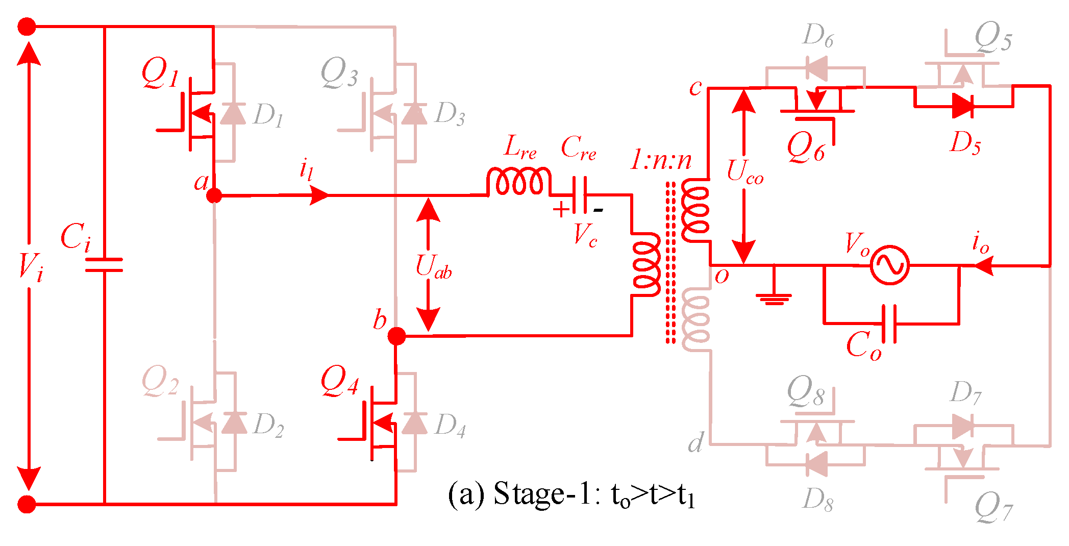
  • A DAB converter is proposed in this paper, which fulfills the galvanic isolation requirement by employing a high-frequency center-tapped transformer between the primary and secondary sides. The primary side consists of a full bridge topology and a resonant tank for soft switching and at the secondary side pairs of anti-series MOSFETs are employed at both ends of the center-tapped transformer, which blocks the reverse current.
  • A novel modulation scheme that is based on the FFM is employed and verified. With the implementation of the proposed modulation scheme in discontinuous conduction mode (DCM), the performance of the converter is considerably improved due to reduced power losses, as the switching losses are minimized with the help of soft switching, and the conduction losses are reduced by blocking the reverse current.
  • The proposed modulation method extends the voltage gain of the converter without compromising the soft switching or adding any complexity to the modulation method. Therefore, improved reliability and voltage gain are achieved in this research without employing any auxiliary components.
The remaining organization of this paper includes the following sections: In Section 2, the background of the suggested topology is explained in detail along with the suggested modulation scheme. In Section 3, operational modes of the proposed topology are described. Section 4 contains the explanation of the control approach employed by the suggested converter. The power losses curves and efficiencies of existing and suggested converters are compared in Section 5. The simulation and experimental results are given in Section 6 and Section 7, respectively. Finally, in Section 8, decisive comments for the suggested converter are specified.

2. Background of the Suggested Converter

2.1. Proposed Converter

The schematic illustration of the suggested series resonant converter (SRC) is presented in Figure 1. Here it is considered that the PV module generates the maximum power with constant DC. The full bridge on the primary end is comprises four MOSFETs (Q1 to Q4) switches alongside their body diodes (D1 to D4) in an antiparallel manner. The center-tapped (CT) bridge on the secondary side is composed of two limbs, where each limb has two MOSFETs (Q5, Q6, and Q7, Q8) with their body diodes (D5 to D8) in an anti-parallel fashion. The resonant LC tank is cascaded with CT-HFT, and this combination is positioned in between the two bridges. The diodes of the primary end facilitate the backflow of current and hence allow the power to flow in reverse mode. In comparison, the CT bridge does not permit the backflow of current and blocks the reverse current. When both the switches of a limb (Q5, Q6 or Q7, Q8) in the CT bridge are turned off then no current will flow in that limb and vice versa. Similarly, a limb with one conducting switch (i.e., Q5) will only allow the stream of positive current via that limb and the non-conducting switch of the limb will block the flow of negative current (i.e., Q6). The stream of current depends upon the input signal and the direction of power flow can be switched by adjusting the input signals of the MOSFETs.
To improve the flow of current and power density, the inductor Lre and capacitor Cre of the resonant tank are connected in series with the CT-bridge and the high-frequency transformer (HFT). The input voltage to the resonant tank is the output of the input side full bridge, which is denoted by Uab, while Uco and Udo represent the output side CT bridge voltages. The two CT-bridge voltages are employed to define the magnitude and phase of the system. If Udo is positive, then the lower limb of the CT bridge will conduct and vice versa. Moreover, bipolar-voltage generation leads to complexity in the control of switches, which becomes very hard and needs suitable modulation techniques to adopt soft switching and ensure high effectiveness.
The conduction and switching features of existing DAB converters and the proposed converter are compared in Table 1. The conventional DAB equipped LC-tank topologies control the power by regulating the duty ratio of the used square wave. Nevertheless, due to the hard switching strategy, these topologies are threatened by higher switching losses [16]. The comparison chart of the proposed topology with other methods is given in Table 2.

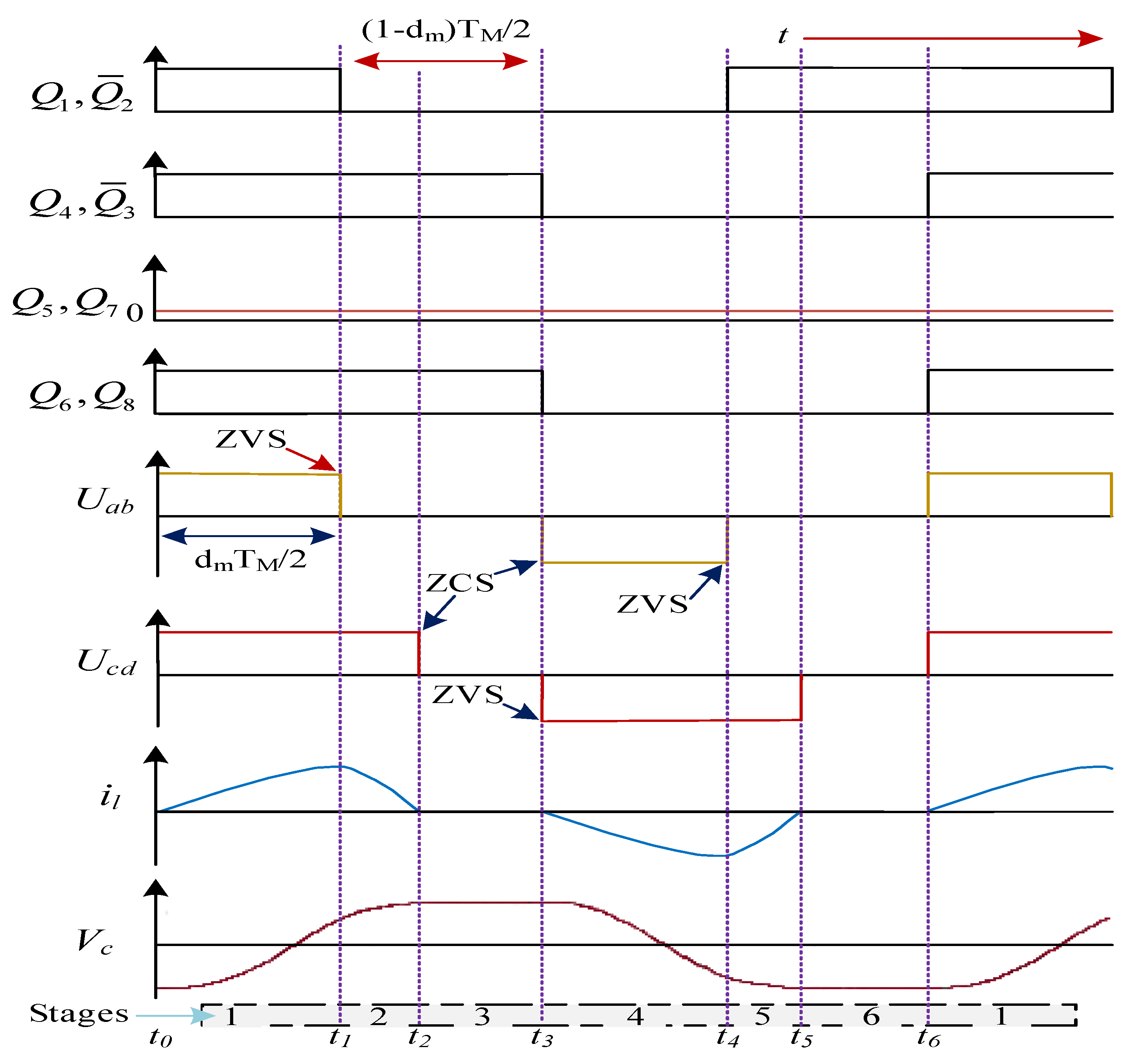
2.2. Fixed Frequency Modulation (FFM)

The working procedure and effective outcomes of the proposed series resonant converter (SRC) under the proposed modulation are presented in Figure 2. Where the modulation frequency (fM) is similar to the resonance frequency of the LC circuit and is given in Equation (1).
f M = ω r e 2 π = 1 2 π L r e C r e
T M = 1 f M
where Lre and Cre correspond to the inductance and capacitance values of the LC-tank circuit.
The amplitude of the output current is controlled by the phase shift at the input side of the converter. The MOSFETs of the full bridge will always work in a complementary manner. In Figure 2, the term 1 − dm represents the phase shift ratio between any two complementary switches working at the same instant, where dm is the duty ratio of the output voltage Uab of the input side full bridge. The proposed SRC works into six stages, where stages three and six are named t3 = TM/2 and t6 = TM. These two stages make up half of the operational waveform. Furthermore, stage one and stage four shared similar time interludes and were given as t4 = t1 + TM/2. Likewise, the time breaks of stage two and stage five are equal and are represented as t5 = t2 + TM/2.
The current il of the tank circuit in stage one and stage two is above zero due to which the tank voltage Vc starts raising. In contrast, the il in stage four and stage five is below zero, and therefore the voltage Vc starts falling. Moreover, the tank voltage will remain unchanged in stage three and stage six as the il stays at zero in these two stages. For ease, the secondary side voltage (Vo) is transformed into the primary side voltage ( V o ) by dividing it by the turns ratio (n) of the HFT as given in Equation (3).
V o = V o n
There will be no energy transfer from input to output ends of the converter if (Vi > V o ) is not followed. Additionally, the switches Q5 and Q7 will block the backflow of current, and therefore no power will conduct until Vi becomes greater than V o . Here, it is presumed that the DC-link capacitances at input and output ends are sufficient enough, hence the voltages Vi and Vo are considered constant during the working of converter. The operational waveforms of the respective stages are given in Figure 2.

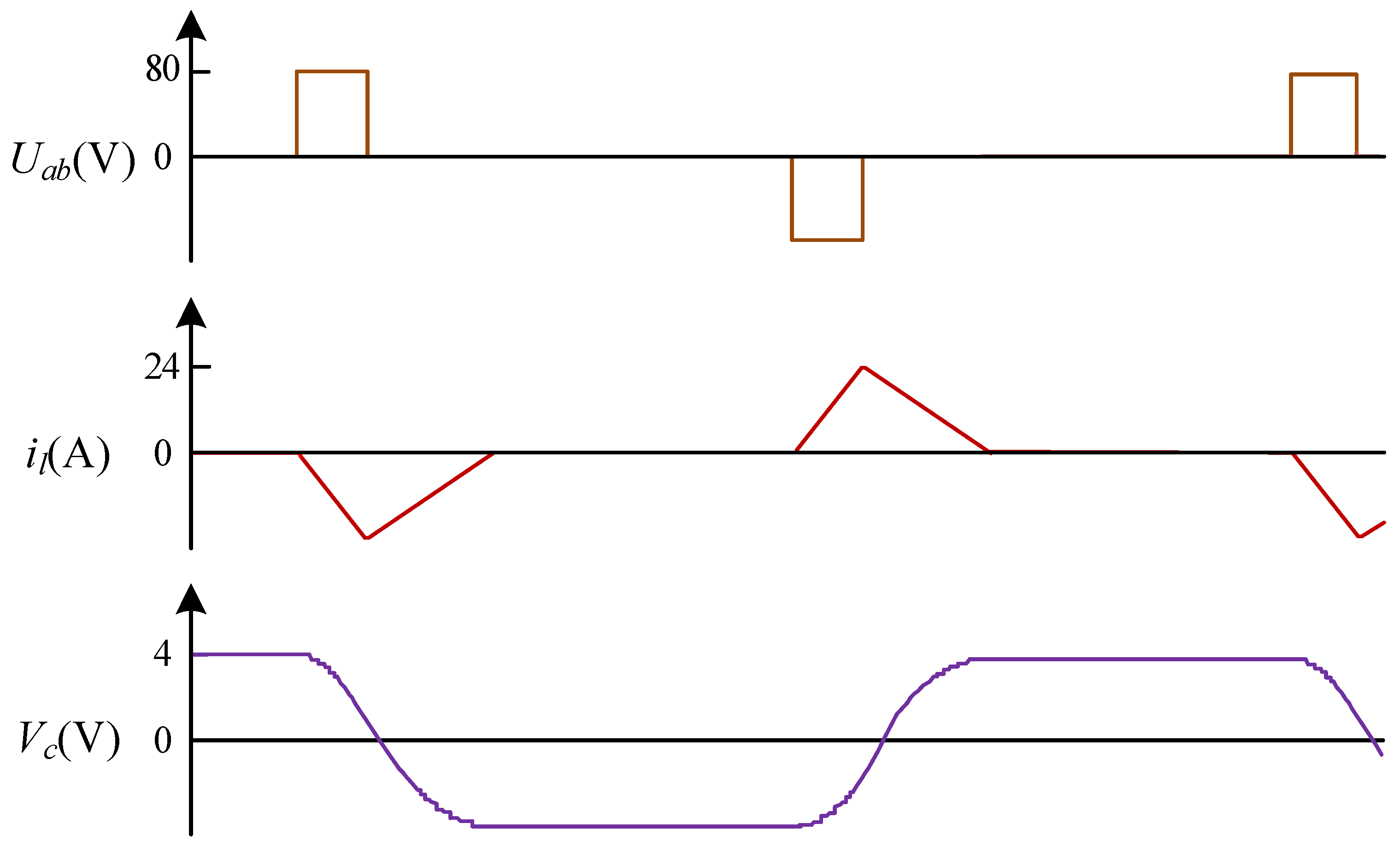
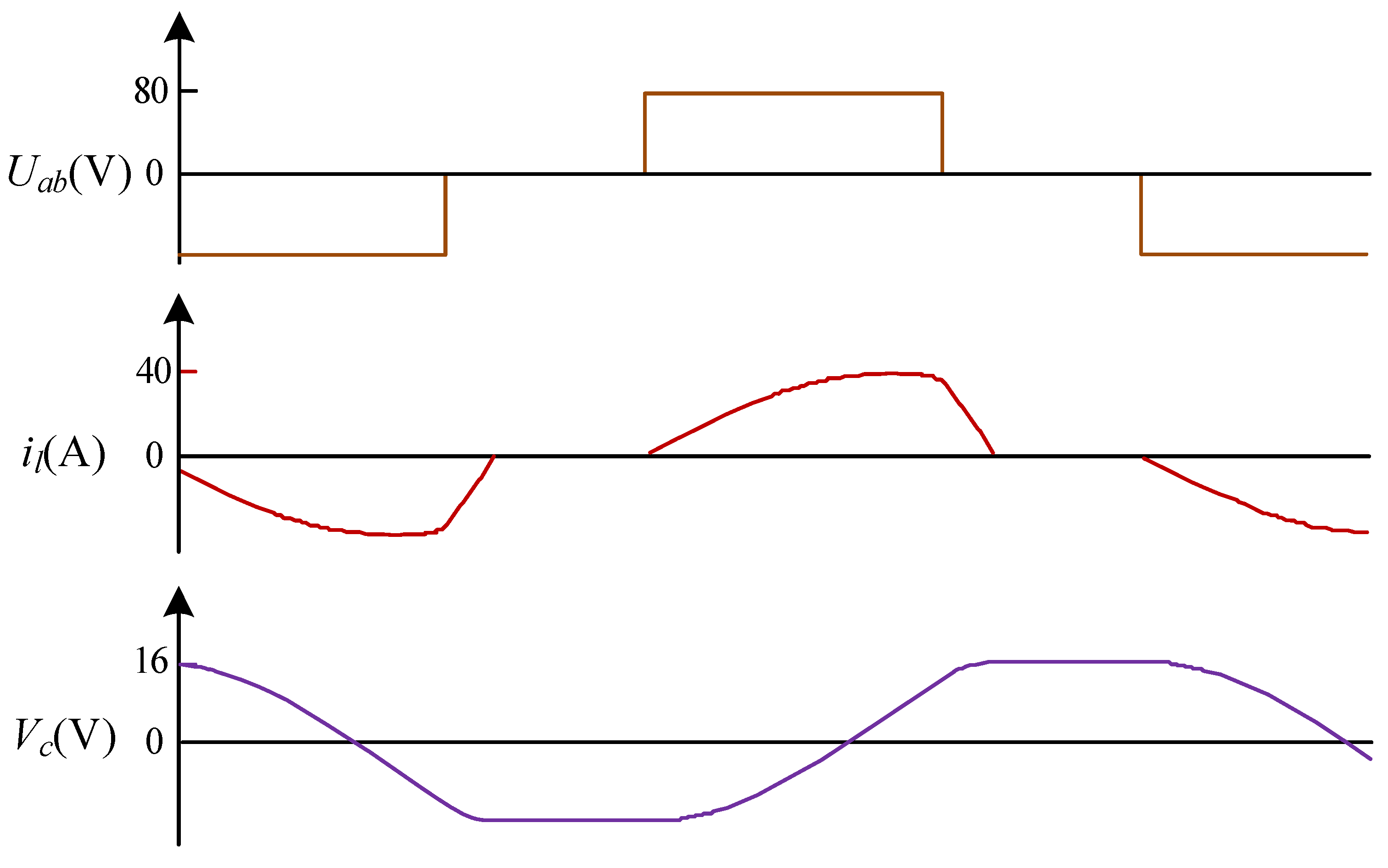
3. Operation Modes of the Proposed Converter
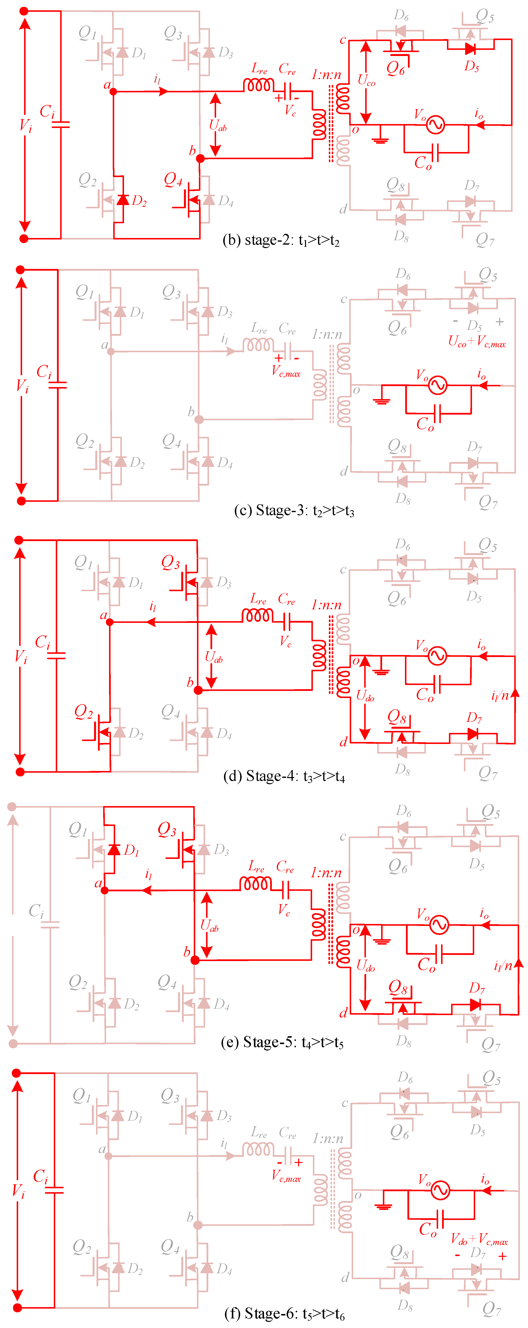
The working stages of the suggested LC-DAB series resonant converter are explained in detail in Figure 3. It operates in six stages. Originally, there is no path for current to stream, therefore no inductor current il will flow as expressed in Equation (4).
i l ( t 0 ) = 0
Similarly, the voltage Vc remains at the lowermost position as given in Equation (5).
V c ( t 0 ) = Δ V c
The primary and secondary sides are detached. Therefore, no power will be transformed between the full bridge and CT-bridge.

3.1. Stage 1

The switches Q1, Q4 of the input side and Q6 of the CT-bridge with antiparallel diode D5 start conducting on ZCS in this stage [t0 < t < t1], as shown in Figure 3a. The total voltage in the resonant circuit at this point is equal to Vi V o . The il begins to grow up gradually and reaches its highest point as given in Equation (6).
L r e d i l d t = V i ( t ) + V c ( t ) V o ( t )
Moreover, within the limits of [0 ≤ tt1], the voltage Vc is discharged to zero, as stated in Equation (7). In this stage, the output end MOSFET Q6 is successively conducting at the line frequency.
C r e · V c ( t ) = 0 t i ( t ) l + V c ( t )

3.2. Stage 2

In this mode [t1 < t < t2], Q1 is turned off and the switch Q2 is turned on at ZVS, as shown in Figure 3b. At the output end, the switch Q6 and the diode D5 remain in working mode just as in stage 1. Moreover, at time t2, the negative tank current il will reach zero level and the tank voltage will touch its highest point. The switch Q3 will not conduct until and unless switch Q2 releases all its energy via D2. The tank current il1 at t1 is achieved by using Equation (8).
i l 1 = ( H + V c ) L r e C r e sin ( ω r e t 1 )
where, H = V0Vi; the reductions of il to zero level is given by Equation (9).
i l 2 = i l 1 cos ( ω r e t 2 ) + ( H 1 V c ( t 2 ) C r e L r e sin ( ω r e t 2 )
where, H1 = −V0; furthermore, the resonant capacitor of the tank Cre reaches it maximum voltage and is shown in Equation (10).
V c ( t 2 ) = V c ( t 1 ) + w x y + z ω r e C r e
where, w = i l 1 sin ( ω r e t 1 ) , x = i l 1 sin ( ω r e t 2 ) , y = ( H 1 V c ( t 1 ) ) C r e L r e cos ( ω r e t 2 ) , and z = ( H 1 V c ( t 1 ) ) C r e L r e .
The term t2 can be calculated by employing Equation (11).
t 2 = π 2 cos 1 ( sin ω r e t 1 ) ω r e + t 1
The duty ratio of input side H-bridge is stated in Equation (12).
d m = 2 t 1 T M

3.3. Stage 3

In this interval, the current il stays at zero level in the tank circuit and hence the diode D5 stops conducting. The time interval of this stage is [t2 < t < t3], as shown in Figure 3c. The switch Q5 at the output end will prevent the current from flowing in the reverse direction. Here, the voltage across Q5 is equal to [Vcmax + Vo]. This stage is called zero current stage because it guarantees the moment of current in one direction (i.e., towards the secondary end) and consequently the next stage starts with the current level at zero. Furthermore, no change in the tank voltage and current is recognized and this explains why both stay at the same level in this stage.

3.4. Stage 4

During this mode [t3 < t < t4], the other switches Q2, Q3 and Q8 start working with D7 at ZCS, as shown in Figure 3d. This sequence generates a negative Uab at the output of the full bridge. At this point, the tank voltage Vc starts decreasing from its highest level, which is equal to ( V o V i ) , and the tank current il moves towards the negative plane. Both the parameters of the LC tank are opposite to each other, as discussed in stage 1.

3.5. Stage 5

In this stage [t4 < t < t5], due to the backflow of current the switch Q1 begins to conduct (i.e., at ZVS), as shown in Figure 3e. Moreover, at time t4, Q2 is turned off and the capacitor voltage Vc in the tank is equal to V o . The tank current il is increased again to zero and the tank voltage is increased back to its highest point, Vcmax.

3.6. Stage 6

This interval [t5 < t < t6] is the same as stage 3, as shown in Figure 3f. In this stage, due to the zero level of tank current, the diode D8 stops conducting naturally. The current in the LC circuit stays at zero until the next mode starts. Moreover, the negative voltage [nVcmax + Vo] is blocked by the switch Q7. This mode remains until the new cycle begins at 1/fM.

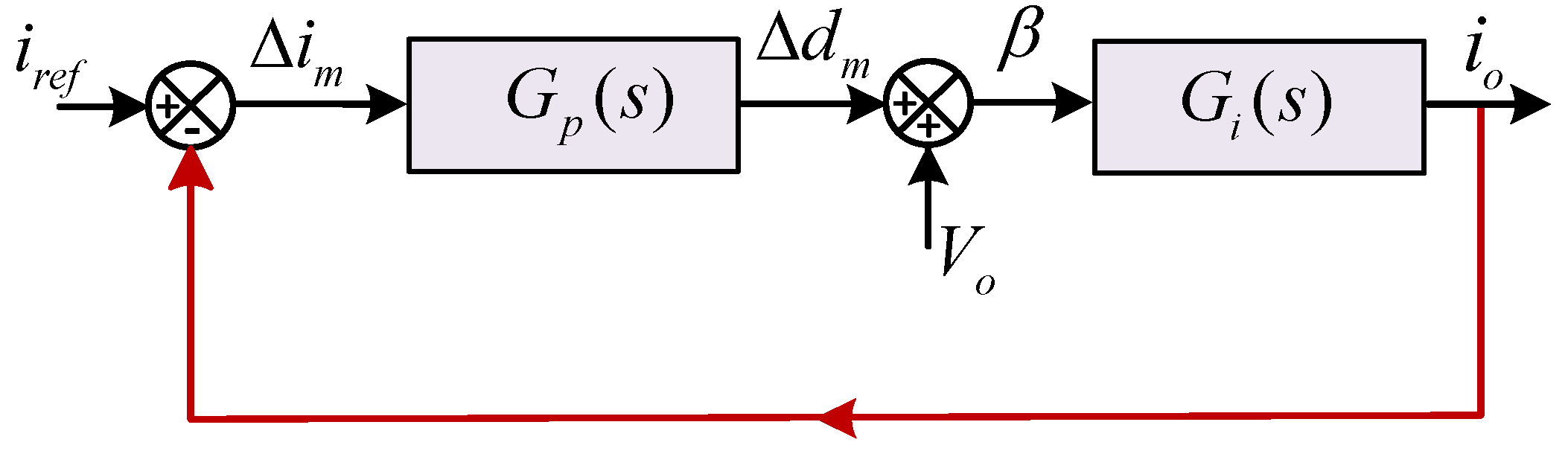
4. Design of the Closed Loop Current Control

This part implements a closed loop current control for the suggested SRC, as shown in Figure 4. Through the utilization of the closed loop, the current reference irf has been successfully tracked. The transfer function of the controller is denoted by the symbol Gp(s) in Figure 4, and the transfer function of the converter is shown by the symbol Gi(s). The value of the irf is decided upon in accordance with the power rating of the converter during the process of forming the control loop. The output of the converter is used as feedback at a reference point, and a proportional-integral (PI) regulator is utilized in order to achieve the desired level of compensation.
The PI controller eliminates the error from the signal and produces a measured current signal. The measured signal is added to the feed-forward loop to produce a firing angle β, which is specified in Equation (13). A modulated input for the switches is produced, which is transformed in the form of β and individual gating PWM signals are produced. These gating signals are applied to the input and output side switches accordingly.
β = cos 1 ( V o V i )
The voltage gain k of the open loop varies with the firing angle under a resistive load. The value of k is calculated by using Equation (14). In contrast, the total time-constant (τ) is estimated with the central time-constant as the modulation frequency has a very small time period compared to the central time-constant. Furthermore, the capacitor at the output end has a more significant impact on the central time constant, as specified in Equation (15).
k = Δ i m Δ d m = 2 π n V i i o ( V i V o + i o / 8 π C r e L r e C r e ) V o ( 2 V o V i V i cos ω r e t r e )
τ = n 2 V o C o i o
The values of the PI regulators parameters are selected according to the highest attainable gain, so that the proposed SRC can provide sensible performance and remain in a stable state. Hence, the appropriate transfer function for the PI controller can be stated as:
G p ( s ) = k i . 1 + T i . s T i .
with the limits, k i . = 1 k max , T i . = τ .

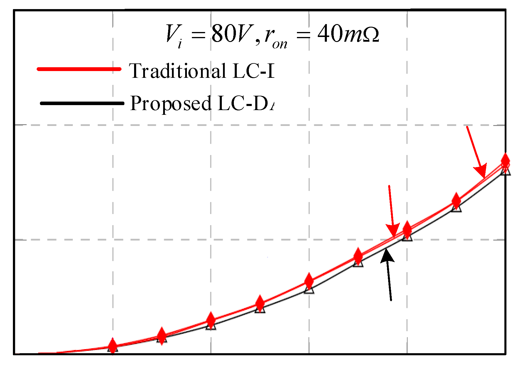
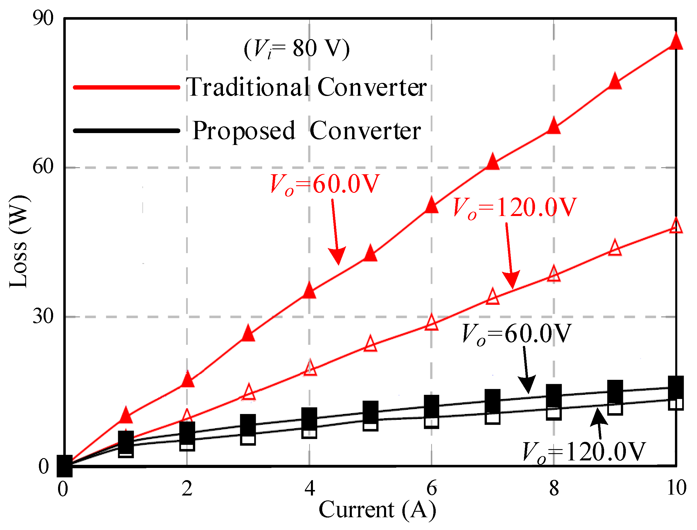
5. Converter Power Losses

In converters, conduction and switching losses contribute the most losses in the network. In this portion, the proposed SRC is compared with the traditional converters [15,16,22]. The parameters of MOSFETs for calculating switching losses are listed in its datasheet [34].

5.1. Conduction Losses Calculation

The resistance and RMS value of the current describe the conduction losses. The output waveform of the system is symmetrical and therefore, in the steady state the RMS value can be considered as the RMS value of the current in the half cycle. By employing the equations of stage 2 (i.e., Equations (7), (11) and (12)) for the initial half cycle, the RMS current for the proposed SRC under FFM can be achieved, as indicated in Equation (17).
I R M S , M = 2 T M ( 0 t 1 , M i r e 2 d t + t 1 , M t 2 , M i r e 2 d t + 0 )
There are three terms in the RMS current shown in Equation (17), in which the first term is from stage 1, the second term is from stage 2 and the third term is from stage 3. The conduction losses in the proposed SRC based on FFM is nearly the same as the conventional LC-DAB topology, as shown in Figure 5. The losses in the proposed topology mostly occurred when the current reached DCM. In the same way, Figure 5 demonstrates that the conduction losses for existing topology rise marginally with a rise in output voltage.

5.2. Switching Losses Calculation
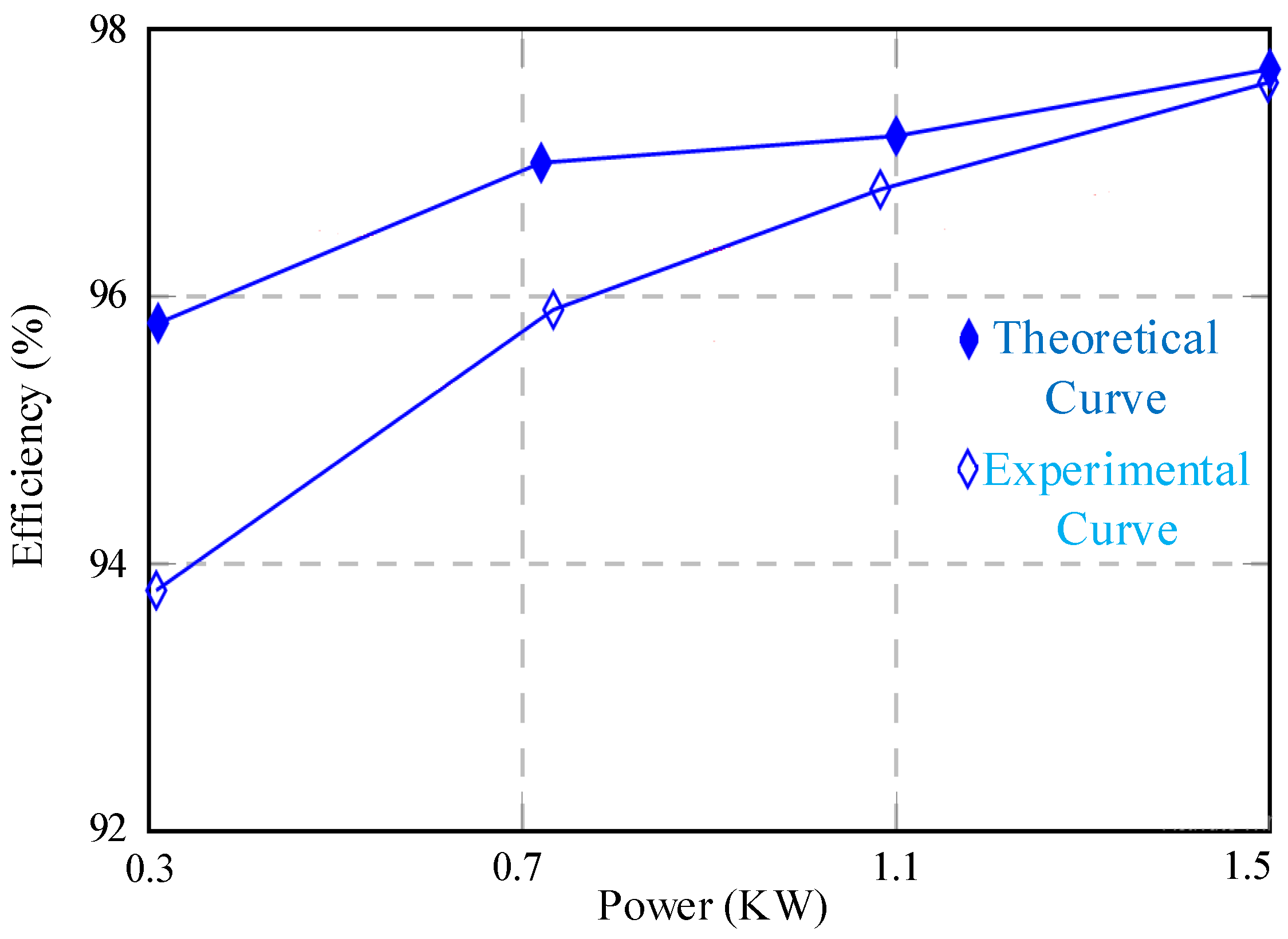
The other losses, which affect the system efficiency, are switching losses. The conventional converter contains two modes of hard switching and two ZVS stages in each sequence, which leads to a high extent of switching losses. On the other hand, the proposed topology under the FFM technique provides soft switching on the entire load range. The leading limb (Q1 and Q2) in the full bridge operates under ZVS or ZCS and therefore the snubber circuit is only used for the rated operation current. In contrast, the lagging limbs in the full bridge (Q3 and Q4) are frequently turned on and off at zero current and therefore required no snubber circuitry [29]. Moreover, the CT-bridge switches achieve ZCS in every cycle and hence do not require a snubber circuit. Although the switching losses are greatly reduced by using the soft-switching technique, some losses still occurred in the switching process of the converter. These losses are measured approximately by employing the current and voltage equations given in [28]. The current at the switching time Isp is shown in Equation (18).
I s p , M = i ( t 1 , M ) = ( E + V C ) L r e C r e ( sin ( ω r e t 1 , M ) )
The total losses produced by the switching pattern under the proposed modulation are specified in Equation (19), where tri denotes the rising time.
P s p , M = V i I s p , M t r i 2 T M
The diagram for switching losses is presented in Figure 6, in which the losses for the proposed converter under FFM are lower than those of the traditional LC-DAB converter. The curves shown in the figure for the proposed converter at two different output voltage values are close to each other with a small gap at higher current values. Whereas in the existing LC-DAB topology, the switching losses increased intensely for lower output values due to a hard switching pattern. In addition, the gap between the two curves is significantly wider at higher current values for the existing LC-DAB converter.

5.3. Efficiency

The total losses for the ideal inductor and transformer are equivalent to the amount of conduction and switching losses present in a system, as illustrated in the efficiency curves in Figure 7. The switching losses added generally in lighter loads, while the conduction losses control the total losses in heavier loads. The proposed topology under the FFM scheme displays improved performance in the case of both heavier and lighter loads. Moreover, the efficiency of the system shows that with a rise in the output voltage, the operative region of the proposed converter is also prolonged. In contrast, the operative range of the existing LC-DAB is tightened due to high extent of switching losses, which leads to decreasing efficiency. The distribution of the power increases with a rise in output voltage and therefore the efficiency of both the topologies increases. For 60 V (output voltage), the proposed topology gives over 91% efficiency, whereas the existing topology offers less than 85% efficiency. Moreover, for 120 V (output voltage), both topologies offer above 95% efficiency in most of the current ratings.

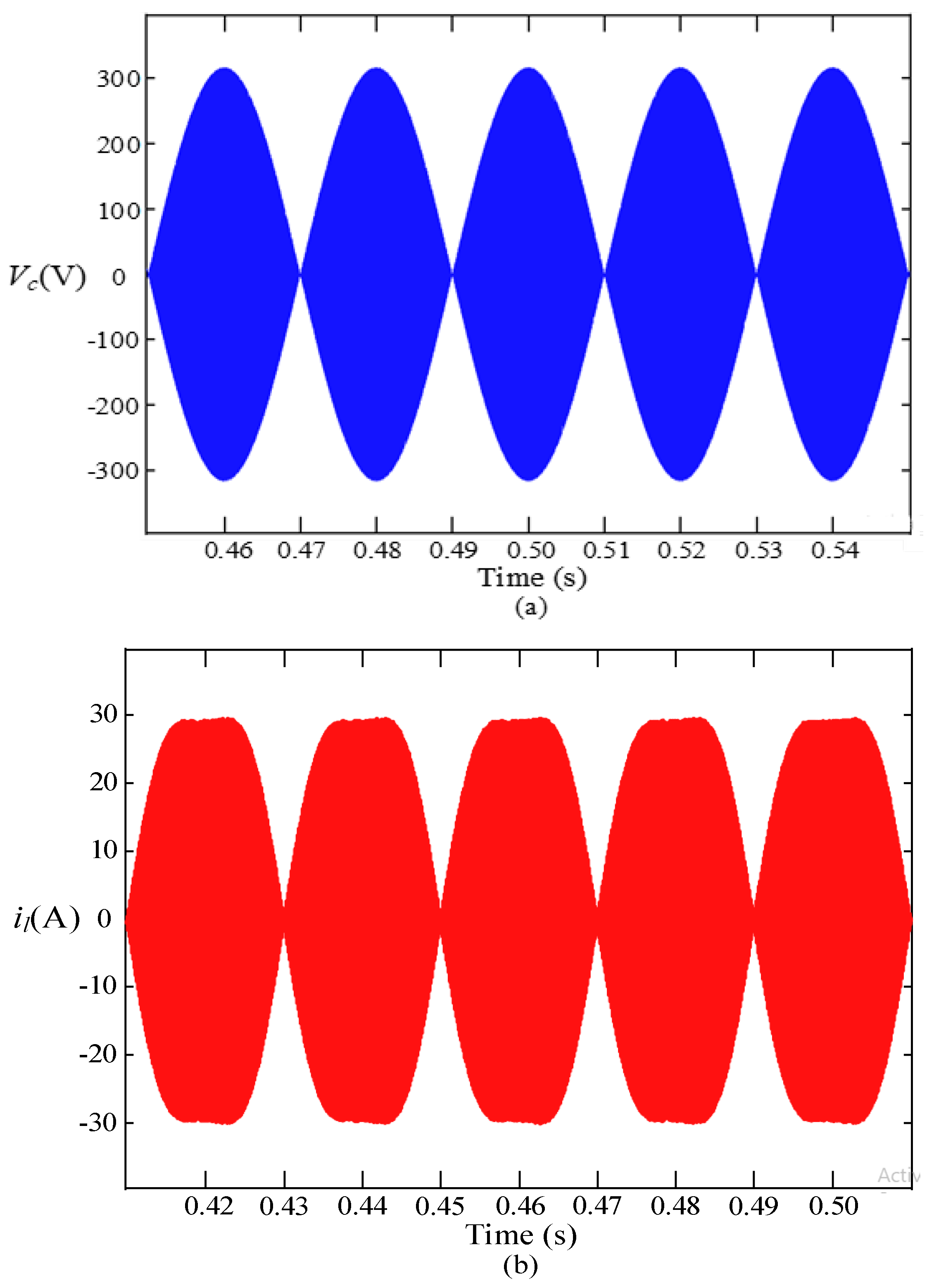
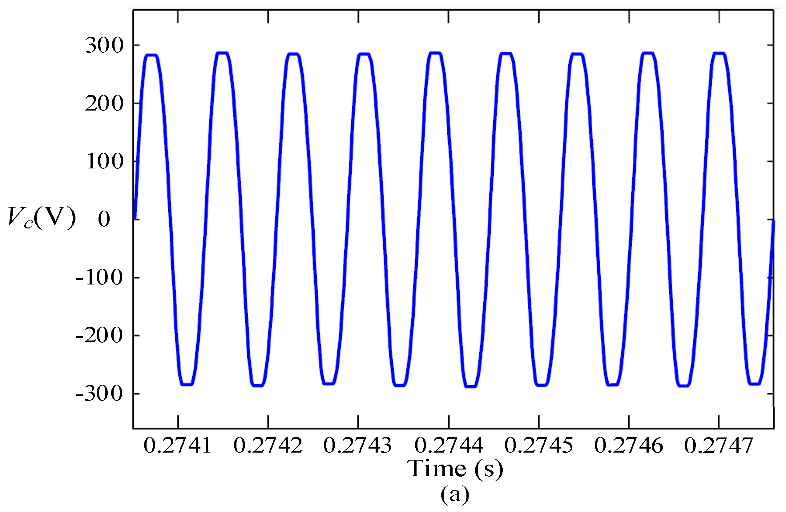
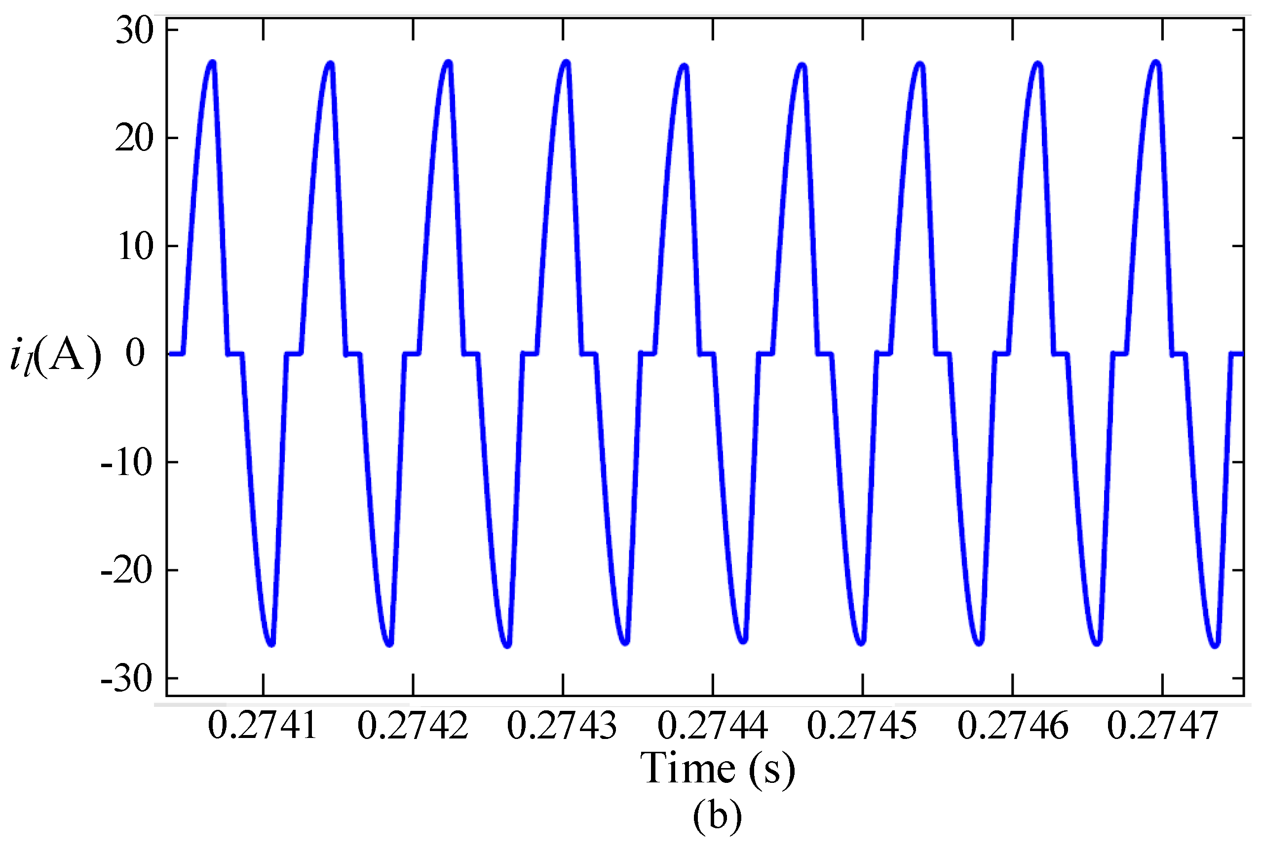
6. Simulation Results

In this part, a Simulink model of the suggested converter was constructed in a MATLAB environment. The model is supposed to be an ideal, where the parasitic resistance is ignored. The results obtained from simulation determine the correctness of the theoretical idea, including blocking of reverse current, calculation of duty cycle and pattern of the gate signal. The tank inductor current il and voltage across the capacitor Vc waveforms at 98% duty ratio are shown in Figure 8. The zoom-in plots of the il having three levels are presented in Figure 9b, where the harmonics content is mitigated in il and this is achieved by using the capacitor in the tank circuit, as shown in Figure 9a. In Figure 9b, the charging and discharging of il can be observed, which happens according to the boundary conditions discussed in Section 2.
The waveforms of the output voltage of the full bridge Uab, inductor current il, and capacitor voltage Vc across the tank are presented at 0.15 duty cycle (Vi = 80 V and Vo = 50 V) in Figure 10. The duty cycle is raised to 0.7 (Vo = 160 V) in Figure 11. In both figures, the current returns and stays at zero until the beginning of a new switching mode, which operates in discontinuous conduction mode (DCM). The results support the precise anticipation of current and voltage in Section 2 and Section 3, whereas the boundary conditions are achieved at the derived turns ratio and the resonance frequency. In both cases, the output current io is fixed at Figure 9a.

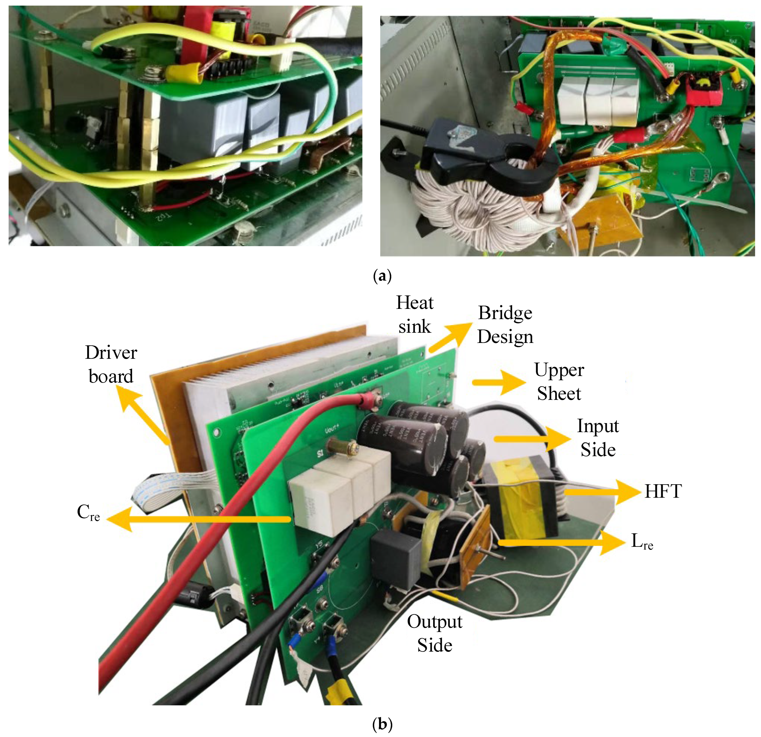
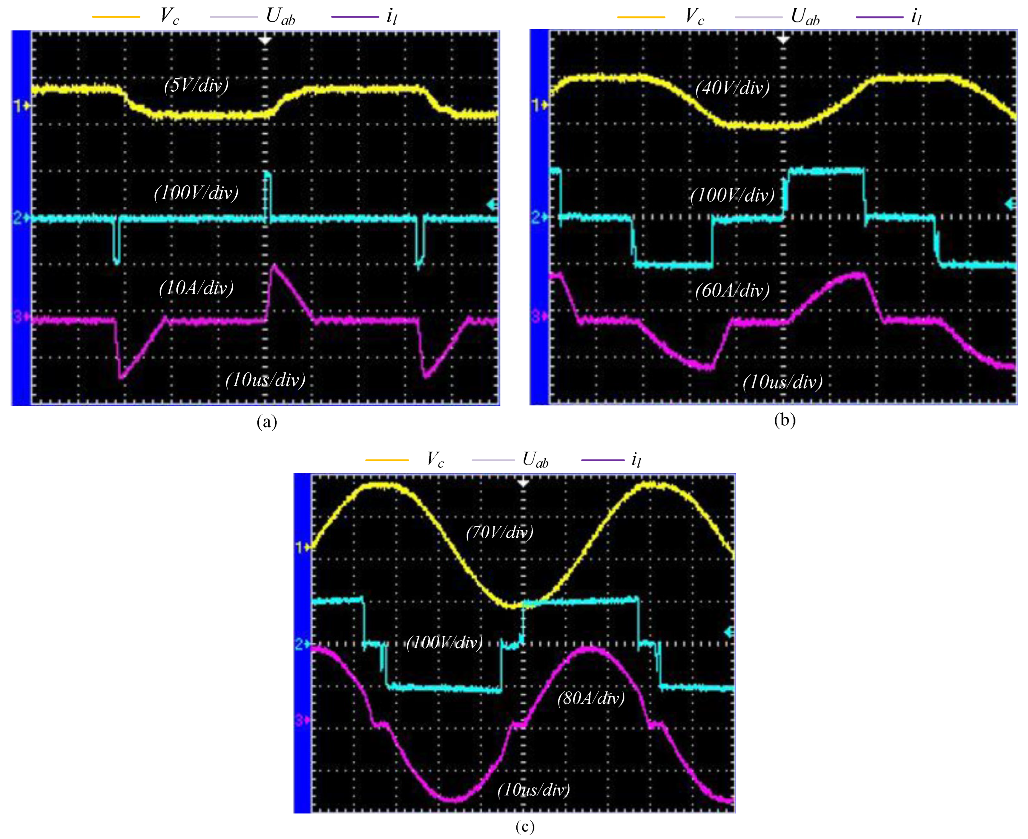
7. Experimental Results

In this part, a 1.5 kW laboratory prototype was designed and tested to determine the feasibility and efficacy of the proposed converter and modulation technique. Generally, the prototype is printed on PCB, which includes MOSFET (IRPF4668, 200 V) on the primary side and MOSFET (IPW60R045CPA, 600 V) on the secondary side, opt coupler IC (HCPL2232), DC/DC converter (24 V–15 V), IC (tpsw2812), IC (UCC27712-Q1) and electronic components consist of diodes, resister, and capacitor, and their values are presented in Table 3. Moreover, a ferrite core inductor (EE70/68/19) and a ferrite core CTT (PC40 EE70) were used. The experimental setup diagram of the proposed converter is shown in Figure 12. Besides, Figure 12a shows the initial setup of the converter in the lab and Figure 12b presents the final setup of the proposed converter.
Each switch pair was set to a dead time of 2 μs. The DSP kit was used for controller coding and the FPGA kit was employed to produce modulation signals. The control board was mounted on the opposite end of the heatsink to reduce the effect of electromagnetic waves. The ADC on DSP calculates the input voltage, output current, and output voltage. Figure 13 displays the operation of the proposed topology for various duty ratios. Initially, the duty cycle was set to 0.1 in Figure 13a, where the tank circuit acts more as an L tank due to small current and less contribution of capacitor voltage. In the prototype, the LC tank behavior depicted when the tank voltage reached 0.6 of the input side voltage. With increasing tank voltage, the dipping time of the waveform also reduces. The duty ratios in Figure 13b,c, are beyond 0.6. In these two cases, the resonance time never surpasses 0.5 of the total duration. Furthermore, a pair of ZVS and ZCS for turned-on condition of the switch in each cycle for the proposed converter under the proposed modulation scheme can be noticed in Figure 13.
The power was measured at the input and output ends by employing a DC meter. The efficiency curve achieved from the experiment is compared with the theoretical curve, as presented in Figure 14. The curves are close to each other at heavier loads, however a small gap can be noticed at smaller and medium powers. This gap may occur due to the aging of MOSFETs and inner resistance of passive components, which were excluded in the theoretical scheme. However, the gap between the output curves is not significant enough and therefore confirms the exactness of the suggested topology.

8. Conclusions

In this paper, an FFM modulation-based soft-switched isolated SRC has been proposed. The proposed converter has the capability to prevent reverse power flow in order to decrease conduction losses and enhance converter efficiency. Moreover, with the implementation of the FFM in DCM, the performance of the converter is considerably improved due to reduced power losses, as the switching losses are minimized with the help of soft switching, and the conduction losses are reduced by blocking the reverse current. The proposed converter has fewer passive components in the resonant tank than other resonant DAB topologies, making it easier to reduce size and obtain higher power densities. Capacitor use in the resonant tank of the proposed converter can assist in minimizing inductor and transformer saturation, which is one of the key concerns for converter topologies. Further, with this topology, zero impedance at resonance frequency is made possible, which is very desirable. Moreover, the performance of topology is further boosted by employing an advanced modulation technique. Besides, the experimental prototype has attained a high operational efficiency of about 97.6% by employing the proposed modulation scheme. Furthermore, the soft-switching method is identified and switching devices’ protection is improved. The suggested control method and structure were simulated and verified using an experimental prototype of 1.5 kW.

Author Contributions

Conceptualization, D.K. and P.H.; methodology, D.K., P.H., M.Y.A.K., M.W., M.T. and A.A.; software, D.K. and M.Y.A.K.; validation, D.K., P.H. and A.A.; formal analysis, D.K., P.H., M.Y.A.K., M.W., M.T. and A.A.; investigation, D.K., P.H., M.Y.A.K., M.W., M.T. and A.A.; resources, D.K., P.H., M.Y.A.K., M.W., M.T. and A.A.; data curation, D.K.; writing—original draft preparation, D.K. and M.W.; writing—review and editing, D.K., P.H., M.Y.A.K., M.W., M.T. and A.A.; visualization, D.K., P.H., M.Y.A.K., M.W., M.T. and A.A.; supervision, P.H.; project administration, P.H.; funding acquisition, M.W. and A.A. All authors have read and agreed to the published version of the manuscript.

Funding

This research received no external funding.

Institutional Review Board Statement

Not applicable.

Informed Consent Statement

Not applicable.

Data Availability Statement

The data supporting the reported results are available in the manuscript.

Acknowledgments

This project was supported by the Estonian Centre of Excellence in Zero Energy and Resource Efficient Smart Buildings and Districts, ZEBE, grant TK146, funded by the European Regional Development Fund to support this research.

Conflicts of Interest

The authors declare no conflict of interest.

References

  1. Ali Khan, M.Y.; Liu, H.; Yang, Z.; Yuan, X. A Comprehensive Review on Grid Connected Photovoltaic Inverters, Their Modulation Techniques, and Control Strategies. Energies 2020, 13, 4185. [Google Scholar] [CrossRef]
  2. Tahir, M.; Ahmed Khan, S.; Khan, T.; Waseem, M.; Khan, D.; Annuk, A. More electric aircraft challenges: A study on 270 V/90 V interleaved bidirectional DC–DC converter. Energy Rep. 2022, 8, 1133–1140. [Google Scholar] [CrossRef]
  3. Salem, A.; Ahmed, E.M.; Orabi, M.; Ahmed, M. Study and Analysis of New Three-Phase Modular Multilevel Inverter. IEEE Trans. Ind. Electron. 2016, 63, 7804–7813. [Google Scholar] [CrossRef]
  4. Waseem, M.; Lin, Z.; Liu, S.; Zhang, Z.; Aziz, T.; Khan, D. Fuzzy compromised solution-based novel home appliances scheduling and demand response with optimal dispatch of distributed energy resources. Appl. Energy 2021, 290, 116761. [Google Scholar] [CrossRef]
  5. Waseem, M.; Lin, Z.; Liu, S.; Sajjad, I.A.; Aziz, T. Optimal GWCSO-based home appliances scheduling for demand response considering end-user’s comfort. Electr. Power Syst. Res. 2020, 187, 106477. [Google Scholar] [CrossRef]
  6. Doncker, R.W.A.A.D.; Divan, D.M.; Kheraluwala, M.H. A three-phase soft-switched high-power-density DC/DC converter for high-power applications. IEEE Trans. Ind. Appl. 1991, 27, 63–73. [Google Scholar] [CrossRef]
  7. Aziz, T.; Lin, Z.; Waseem, M.; Liu, S. Review on optimization methodologies in transmission network reconfiguration of power systems for grid resilience. Int. Trans. Electr. Energy Syst. 2021, 31, e12704. [Google Scholar] [CrossRef]
  8. Sun, X.; Wang, Z.; Zhang, Q.; Chen, G. Variable frequency triple-phase-shift modulation strategy for minimizing RMS current in dual-active-bridge DC-DC converters. J. Power Electron. 2021, 21, 296–307. [Google Scholar] [CrossRef]
  9. Rizwan, M.; Waseem, M.; Liaqat, R.; Sajjad, I.A.; Dampage, U.; Salmen, S.H.; Obaid, S.A.; Mohamed, M.A.; Annuk, A. SPSO Based Optimal Integration of DGs in Local Distribution Systems under Extreme Load Growth for Smart Cities. Electronics 2021, 10, 2542. [Google Scholar] [CrossRef]
  10. Tahir, M.; Hu, S.; He, X. Performance Improvement Strategies for Discrete Wide Bandgap Devices: A Systematic Review. Front. Energy Res. 2021, 711. [Google Scholar] [CrossRef]
  11. Waseem, M.; Sajjad, I.A.; Napoli, R.; Chicco, G. Seasonal Effect on the Flexibility Assessment of Electrical Demand. In Proceedings of the 2018 53rd International Universities Power Engineering Conference (UPEC), Glasgow, UK, 4–7 September 2018; pp. 1–6. [Google Scholar]
  12. Khan, D.; Khan, M.M. An Improved Capacitor Current Active Damping Based on Parallel Feed-Forward Compensation Method for LCL Filtered Grid Connected Inverter. In Proceedings of the 2019 4th International Conference on Information Systems Engineering (ICISE), Shanghai, China, 4–6 May 2019; pp. 68–75. [Google Scholar]
  13. Khan, T.; Yu, M.; Waseem, M. Review on recent optimization strategies for hybrid renewable energy system with hydrogen technologies: State of the art, trends and future directions. Int. J. Hydrogen Energy 2022, 47, 25155–25201. [Google Scholar] [CrossRef]
  14. Liu, F.; Chen, Y.; Chen, X. Comprehensive Analysis of Three-Phase Three-Level LC-Type Resonant DC/DC Converter With Variable Frequency Control—Series Resonant Converter. IEEE Trans. Power Electron. 2017, 32, 5122–5131. [Google Scholar] [CrossRef]
  15. Krismer, F.; Kolar, J.W. Efficiency-Optimized High-Current Dual Active Bridge Converter for Automotive Applications. IEEE Trans. Ind. Electron. 2012, 59, 2745–2760. [Google Scholar] [CrossRef]
  16. Li, Y.; Wang, Y.; Song, H. Bidirectional DC-DC Converter based on CLC network. In Proceedings of the 2019 22nd International Conference on Electrical Machines and Systems (ICEMS), Harbin, China, 11–14 August 2019; pp. 1–4. [Google Scholar]
  17. Mustafa, M.; Rizwan, M.; Kashif, M.; Khan, T.; Waseem, M.; Annuk, A. LC Passive Wireless Sensor System Based on Two Switches for Detection of Triple Parameters. Sensors 2022, 22, 3024. [Google Scholar] [CrossRef] [PubMed]
  18. Mansouri, S.; Afjei, E. Performance improvement on dual active bridge converter using CLLC resonant network with separated capacitor and inductor. In Proceedings of the 2017 Iranian Conference on Electrical Engineering (ICEE), Tehran, Iran, 2–4 May 2017; pp. 1032–1036. [Google Scholar]
  19. Niu, J.; Wu, X.; Wang, Y.; Jing, L.; Zhang, W.; Tong, Y. Backward Step-Up Control Strategy for Bidirectional LLC Resonant Converter. Energies 2022, 15, 4471. [Google Scholar] [CrossRef]
  20. Escudero, M.; Kutschak, M.A.; Pulsinelli, F.; Rodriguez, N.; Morales, D.P. On the practical evaluation of the switching loss in the secondary side rectifiers of LLC converters. Energies 2021, 14, 5915. [Google Scholar] [CrossRef]
  21. Hao, W.; Ping, W.; Yaohua, L. A control method for series resonant dual active bridge DC/DC converter. In Proceedings of the 2014 IEEE Conference and Expo Transportation Electrification Asia-Pacific (ITEC Asia-Pacific), Beijing, China, 31 August–3 September 2014; pp. 1–5. [Google Scholar]
  22. Shakib, S.M.S.I.; Mekhilef, S. A Frequency Adaptive Phase Shift Modulation Control Based LLC Series Resonant Converter for Wide Input Voltage Applications. IEEE Trans. Power Electron. 2017, 32, 8360–8370. [Google Scholar] [CrossRef]
  23. Iqbal, M.M.; Sajjad, I.A.; Manan, A.; Waseem, M.; Ali, A.; Sohail, A. Towards an Optimal Residential Home Energy Management in Presence of PV Generation, Energy Storage and Home to Grid Energy Exchange Framework. In Proceedings of the 2020 3rd International Conference on Computing, Mathematics and Engineering Technologies (iCoMET), Sukkur, Pakistan, 29–30 January 2020; pp. 1–7. [Google Scholar]
  24. Rizwan, M.; Hong, L.; Waseem, M.; Ahmad, S.; Sharaf, M.; Shafiq, M. A Robust Adaptive Overcurrent Relay Coordination Scheme for Wind-Farm-Integrated Power Systems Based on Forecasting the Wind Dynamics for Smart Energy Systems. Appl. Sci. 2020, 10, 6318. [Google Scholar] [CrossRef]
  25. Qu, P.; Li, Z.; Wang, P.; Li, Y. An improved analysis considering harmonic components for high-frequency isolated dual-active-bridge series resonant DC-DC converter. In Proceedings of the 2014 IEEE Conference and Expo Transportation Electrification Asia-Pacific (ITEC Asia-Pacific), Beijing, China, 31 August–3 September 2014; pp. 1–4. [Google Scholar]
  26. Tong, A.; Hang, L.; Li, G.; Zhu, M.; Xie, D. Common duty ratio control of series resonant dual active bridge converter. In Proceedings of the 2016 IEEE 2nd Annual Southern Power Electronics Conference (SPEC), Auckland, New Zealand, 5–8 December 2016; pp. 1–5. [Google Scholar]
  27. Safaee, A.; Jain, P.; Bakhshai, A. Time-domain analysis of a wide-range dual-active-bridge bidirectional series resonant converter. In Proceedings of the IECON 2015—41st Annual Conference of the IEEE Industrial Electronics Society, Yokohama, Japan, 9–12 November 2015; pp. 004139–004145. [Google Scholar]
  28. Sato, F.; Shimada, T.; Ouchi, T. Novel Switching Control Method for Full-Bridge DC-DC Converters for Improving Light-Load Efficiency Using Reverse Recovery Current. In Proceedings of the 2018 International Power Electronics Conference (IPEC-Niigata 2018-ECCE Asia), Niigata, Japan, 20–24 May 2018; pp. 250–255. [Google Scholar]
  29. Chen, J.J.; Lin, B.R. Analysis of ZVS/ZCS soft-switching dual-resonant converter. In Proceedings of the 2009 International Conference on Power Electronics and Drive Systems (PEDS), Taipei, Taiwan, 2–5 November 2009; pp. 411–416. [Google Scholar]
  30. Ulissi, G.; Kucka, J.; Vemulapati, U.R.; Stiasny, T.; Dujic, D. Resonant IGCT Soft-Switching: Zero-Voltage Switching or Zero-Current Switching? IEEE Trans. Power Electron. 2022, 37, 10775–10783. [Google Scholar] [CrossRef]
  31. Musavi, F.; Craciun, M.; Gautam, D.S.; Eberle, W.; Dunford, W.G. An LLC resonant DC-DC converter for wide output voltage range battery charging applications. IEEE Trans. Power Electron. 2013, 28, 5437–5445. [Google Scholar] [CrossRef]
  32. Liu, S.; Zhang, F. State variable derivation with numerical approach and efficiency optimisation method for phase-shift LLC converters under wide voltage-gain range. IET Power Electron. 2019, 12, 1752–1762. [Google Scholar] [CrossRef]
  33. Vu, H.; Choi, W. A novel dual full-bridge LLC resonant converter for CC and CV charges of batteries for electric vehicles. IEEE Trans. Ind. Electron. 2018, 65, 2212–2225. [Google Scholar] [CrossRef]
  34. Spaziani, L. A study of MOSFET performance in processor targeted buck and synchronous rectifier buck converters. In Proceedings of the HFPC Power Conversion Proc, Las Vegas, NV, USA, 6–8 January 1996; pp. 123–137. [Google Scholar]
Figure 1. Schematic illustration of the suggested converter topology.
Energies 15 05802 g001
Figure 2. Suggested converter waveforms under FFM.
Energies 15 05802 g002
Figure 3. Working stages of proposed converter (Vo > 0).
Energies 15 05802 g003aEnergies 15 05802 g003b
Figure 4. Diagram of closed loop current control for proposed converter.
Energies 15 05802 g004
Figure 5. Conduction losses waveforms of two LC-DAB converters.
Energies 15 05802 g005
Figure 6. Switching losses waveforms of two LC-DAB converters.
Energies 15 05802 g006
Figure 7. Efficiency waveforms of the two LC-DAB Converters.
Energies 15 05802 g007
Figure 8. Simulation results (a) Resonant capacitor voltage Vc and (b) Resonant inductor current il.
Energies 15 05802 g008
Figure 9. Zoom-in waveforms of (a) resonant capacitor voltage Vc and (b) resonant inductor current il.
Energies 15 05802 g009aEnergies 15 05802 g009b
Figure 10. Simulation results at 15% duty ratio.
Energies 15 05802 g010
Figure 11. Simulation results at 60% duty ratio.
Energies 15 05802 g011
Figure 12. Experimental setup up of the proposed converter (a) Initial designs for the proposed converter in the lab and (b) Laboratory setup of proposed converter.
Energies 15 05802 g012
Figure 13. Experimental outcomes at duty ratios (a) 0.10 (b) 0.70 and (c) 0.9.
Energies 15 05802 g013
Figure 14. Comparison of Power Efficiencies (Vin = 60 V, Vs = 120 V).
Energies 15 05802 g014
Table 1. Assessment of existing and proposed converters.
Converter TypesBackflow of CurrentSwitching Features
L-Tank Topology [6]Allowsoft-switching
LC-Tank Existing Topology [13]Blockhard-switching
LC-Tank Proposed TopologyBlocksoft-switching
Table 2. Comparison Table of Proposed Topology with other Methods.
ParametersConventional LLC [31]Hybrid Control Strategy [32]Dual Full Bridge LLC [33]Proposed
Control stabilitySimpleComplexComplexSimple
Control complexityHighHighHighLow
Accuracy of analysisPoorHighHighHigh
Components designComplicatedMediumMediumSimple
Design methodSimplecomplexcomplexSimple
Soft switching capabilityNarrowmediummediumFull Load
Table 3. Parameter of the Proposed Converter.
ParametersRepresentationValues (Unit)
Input side voltageVi80.0 (V)
Tank inductorLre160.0 (μH)
Maximum Output voltageVo,max160.0 (V)
Tank capacitorCre1.0 (μF)
Output side filter capacitorCo20.0 (μF)
Turn ratiosn1:2.2:2.2
Regulator Parametersk0.800
(PI-controller)t0.000250
Publisher’s Note: MDPI stays neutral with regard to jurisdictional claims in published maps and institutional affiliations.

