Article

Synthesis of 3D Nanonetwork Si Structures via Direct Ultrafast Pulsed Nanostructure Formation Technique

by
Nishant Singh Jamwal
1,2 and
Amirkianoosh Kiani
1,2,*
1
Silicon Hall—Micro/Nano Manufacturing Facility, Faculty of Engineering and Applied Science, Ontario Tech University, 2000 Simcoe St N, Oshawa, ON L1G 0C5, Canada
2
Department of Mechanical and Manufacturing Engineering (MME), Ontario Tech University, 2000 Simcoe St N, Oshawa, ON L1G 0C5, Canada
*
Author to whom correspondence should be addressed.
Energies 2022, 15(16), 6005; https://doi.org/10.3390/en15166005
Submission received: 13 July 2022 / Revised: 5 August 2022 / Accepted: 16 August 2022 / Published: 18 August 2022

Abstract

:
Silicon is one of the most used semiconductor materials around the world. This research was conducted on silicon to improve its opto-electrical properties including bandgap and optical conductivity using direct ultrafast pulsed nanostructure formation (DUPNF). The power and frequency of high-intensity picosecond laser pulses were varied, and nanostructures were formed. The optical properties were examined using optical spectroscopy in both VIS and NIR. The structural characteristics were examined using EDX and SEM imaging. It was found that varying the power and frequency of the laser processing caused a change in the bandgap, as well as the structural characteristics of the silicon semiconductor. Increasing the frequency and power showed the formation of nanostructures of silicon and their variation in the properties of the formed nanostructures. The critical breakdown field of the silicon nanostructures was higher than the bulk silicon.

1. Introduction

With the development of technology and nanoscience, nanomaterials have become a major attraction. The properties of the materials become better in the nanoscale. Furthermore, as the scale is reduced, the size is reduced, thus allowing the material to be used in devices with compact size. This is another need, where we expect devices of reduced size but without any loss in their function. Silicon is one of the most abundantly available semiconductors which has shown several promising aspects for application in various fields such as electronics, biomedical, sensors, and energy generation [1,2,3,4,5,6,7,8]. Silicon has an indirect bandgap of 1.12 eV [9,10] which is pretty low, and this constrains the use of silicon in various high-power applications [11,12]. Another constraint to the high-power application of silicon is its lower critical breakdown field, which is 0.2 MV/cm [13,14,15].
The transition to nanomaterials has allowed us to vary the properties of materials. The properties of nanomaterials are different than the bulk materials. Extensive research has been performed, and many authors have published the nanostructure synthesis of silicon using various techniques such as chemical vapor deposition [16,17], sol-gel technique [18], spray pyrolysis [19], and laser deposition [20,21]. The variation in, for instance, the precursors’ annealing temperatures offers nanostructures with controlled opto-electrical properties. The research has also been moving toward newer novel methods for synthesis, as some of the methods require a very expensive setup and preparation environment. Therefore, a novel method for green and cheaper synthesis of nanostructures of silicon in ambient conditions was previously reported by our group. Our proposed direct ultrafast pulsed nanostructure formation (DUPNF) offers a convenient and single-step procedure for producing nanostructures of silicon with predetermined optical properties [22].
In this research, we report the changes in the properties of the synthesized nanostructures of silicon using DUPNF. We report these changes as a function of laser parameters such as power and frequency. The formation of nanostructures is greatly dependent on the amount of both laser power and energy applied for the process of ablation. Our novel method of synthesizing nanoparticles involves the use of the principle of laser ablation in ambient conditions. The laser interacts with the material, and the energy is absorbed by the substrate; a plasma layer is formed over time. Having ultrashort laser pulses allows us to limit laser and material interaction and helps in controlling the damage to the material. Furthermore, the ultrashort pulses help in the disintegration of the surface into fine particles deposited over the material. Therefore, we varied the power and frequency and verified the effects on the pulse energy and pulse duration of the laser.

2. Materials and Methods

2.1. Experimental Setup

The Silicon n-type (Si-100) wafers of 20 micrometer thickness were used for the experiment. The nanostructures were synthesized by irradiation of silicon using a pulsed fiber laser (IPG Model: YLPP-1-150V-30) at a scan speed of 100 mm/s and pulse duration of 150 ps.
Four samples were created by varying the power and frequency (600, 800, 1000, and 1200 kHz) of the laser. The sets were named ‘S’ and ‘A’ samples. The S samples (constant pulse energy) had varying frequency and varying power (10, 13.3, 16.7, and 20 W) with a constant amount of energy (110 μJ), while the A samples (constant power) had varying frequency, and the power was constant at 15 W. The details are provided in Table 1 and Table 2. The silicon wafer was mounted, and MarkingMate 2.7 software was used for the setting the pattern and various parameters for the samples to be ablated. The nanostructure formation was established at ambient temperature and pressure. The schematic layout of the setup is shown in Figure 1.

2.2. Analysis

The optical tests were carried out on the samples using light spectroscopy (Ocean Optics STS-NIR), and the reflectance spectra were collected and analyzed. SpectraSuite software was employed for recording and analyzing the reflectance curve and data. The setup included a light source, spectrometer, sample holder, and optical cables. The SpectraSuite software was initialized, and, using the reflectance option, the reference was added with the light source on (for light spectrum) and off (for dark spectrum). Then, using the probe, diffuse reflectance data were obtained for all the synthesized samples. Then, to determine the bandgap of the samples, the Kubelka–Munk function was used [23].
( F ( R ) · h ν ) 1 γ = B ( h ν E g ) .
This approach is similar to that of the Tauc plot [24].
( α · h ν ) 1 γ = B ( h ν E g ) .
The difference here is that the diffused reflectance is used to determine the bandgap instead of absorbance. A graph is plotted of ( F ( R ) h v ) n vs. , where is the energy and F(R) is the Kubelka–Munk function; the value of n is based on the direct or indirect bandgap.
k s = ( 1 R ) ) 2 2 R ,
where k is the molar absorption coefficient, and s is the scattering coefficient.
Accordingly, a graph is plotted, and the bandgap value is determined. Table 1 and Table 2 illustrate the values of the bandgaps and the parameters used for the synthesis of the nanostructures of the samples.
The morphology and structural characterizations were performed using SEM and EDX (Thermofisher Quanta 3D LSB) imaging.

2.3. Statistical Analysis

The data collected by spectroscopy were analyzed and processed using Origin pro 2021a. Signal processing was conducted using the weighted average method with a weight of 5 to reduce to the signal noise at a higher corner wavelength. ImageJ analysis was applied to process the SEM image scales.

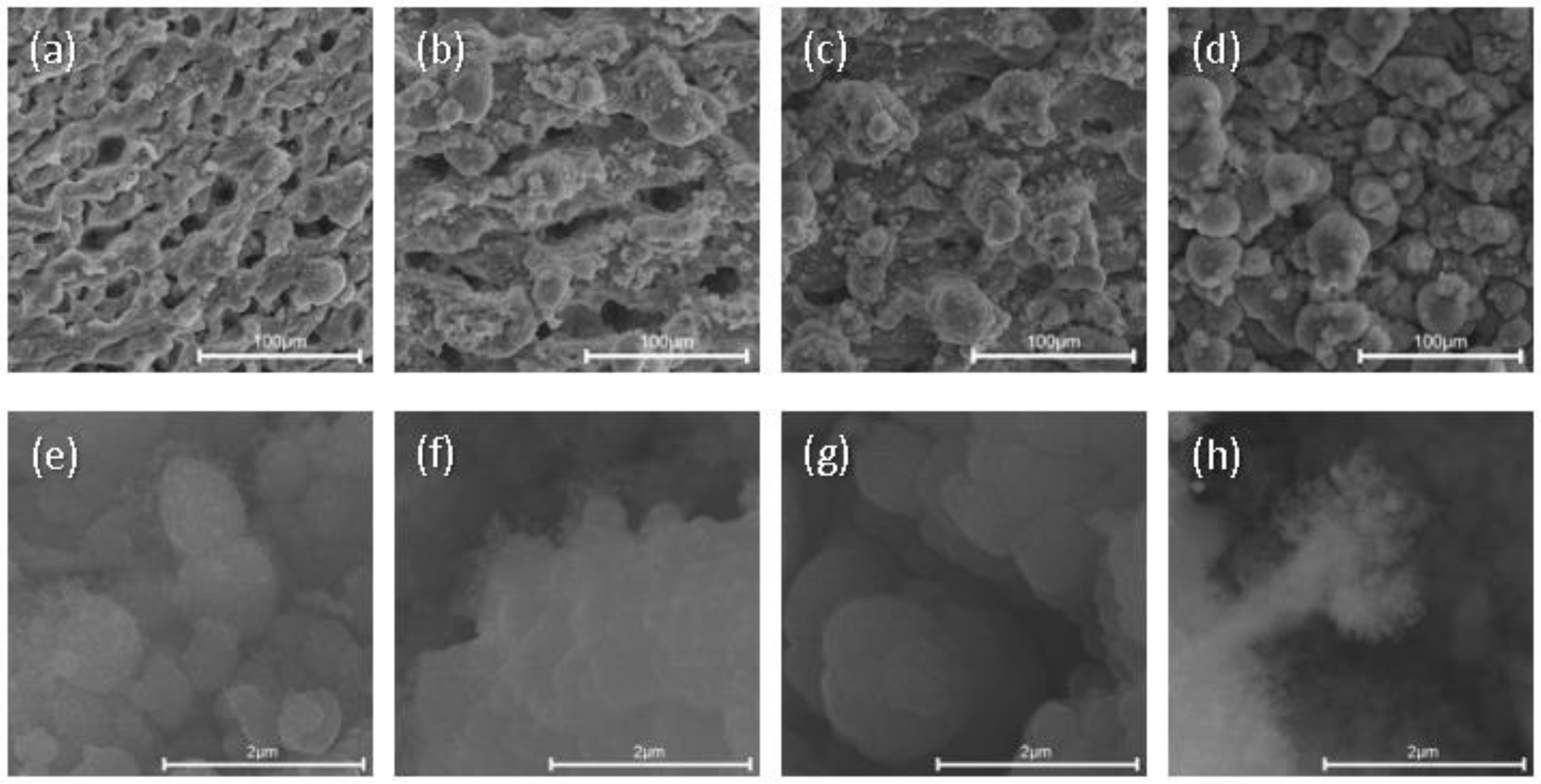
3. Results and Discussion

3.1. SEM

The samples were first inspected via SEM; the images are shown in Figure 2, where it can be clearly observed that the sample S4 had more 3D nanonetwork structures. S1 to S3 samples showed an increase in the brightness (corresponding to the amount of 3D nanonetwork structures) in the area where the DUPNF technique was performed. Furthermore, there was a similar trend in the A samples. A1 to A4 showed that the color of the samples became brighter and lighter. This, was however, lower than that of the S set of samples. The ablated area of S2 and S3 samples was similar to that of the A4 sample when viewed with the unaided human eye.
The SEM images in Figure 2 show the morphology of the nanoparticles of silicon. Here, it can be clearly observed that the formation of nanoparticles was higher in A1; at higher magnification, we can see the small fibers that were formed. Moving forward toward A4, the size of the particles increased. We can see an increase in the number of small particles. This change was observed in the SEM images in the ascending order for the samples. In A1, the particles were fibrous and less integrated. When observing A2 and A3, we can see the particles becoming clusters, and, at higher magnification, we can observe denser fibers. These samples showed a better formation of nanoparticles. A4 had particles with small thinner lines and structures like small cells. In images at higher resolution, it can be seen that, for A4, fibers were produced. The growth was highest in A1 while there were some fibers in A2 similar to A1. The fibers were like small threads coming out of the particles.
The S samples (Figure 3) showed a similar growth to the A samples. Here, the nanoparticle formation increased from S1 to S4. The particles in the S1 were more compact and lesser in quantity. With regard to S2, a difference from S1 can be noted due to the increase in power and frequency for the samples. The formed nanostructures were more like A samples here. For S3, the nanostructures were similar to those of A3 and A4, almost certainly due to the similar parameters for the samples. The difference here was only in the pulse interval for all the samples. Looking at S4, which was synthesized with the highest power and frequency, we can see that the nanostructures exhibited more of a thread formation. These threads were longer and clearly visible even at a lower resolution of 100 μm. At higher resolution, we can see that the threads had smaller threads coming out, forming a fern-like structure. The S set of samples showed a varied concentration and structure of the nanostructures overall. This can be attributed to the change in power. The power was kept constant for the A set of samples; thus, the fiber growth did not vary much. The EDX images (Figure 4) show the variation between Si and O content in the samples. In the A set of samples, it can be noted that the Si and O ratio was quite similar. However, in the case of the S set samples, there was a higher variation in the Si and O content. The Si content was similar for all samples, but a greater difference could be seen in the O content with respect to Si.

3.2. Optical Properties

3.2.1. Bandgap

There was an increase in the bandgap of all the samples. The S and A sets of samples exhibited nanoparticle formation; accordingly, the bandgaps of the samples were significantly enhanced. There were noticeable variations in the bandgaps of all samples. Certain trends were observed for both sets of samples. As can be seen in Figure 5, three different states were observed in the bandgap curve. Similar states were also observed by Shreeniket et al., which were identified as the free carrier, exciton, and fundamental absorbance state [25].
Figure 6 shows the bandgaps of the A samples, where we suspected the effect of quantum confinement on the basis of the SEM images and the results obtained for the bandgap. According to the quantum confinement effect, the bandgap increases as the particle size decreases. The size of the particles under the quantum confinement effect also defines the bandgap size, whereby a smaller size results in a larger bandgap [26,27]. However, quantum confinement cannot be effectively defined solely on the basis of the optical bandgap [28]. For the A samples, although the bandgap was enhanced, there was a decrease in the bandgap when going in ascending order. The decrease in bandgap was related to the decrease in the pulse energy of the samples from A1 to A4, as can be noted in Figure 7. As the pulse energy was reduced, the nanoparticle formation was also decreased. The decline in the energy of each pulse led to lower ablation; accordingly, the bandgap enhancement was lower for the A4 sample. This change was coherent with the SEM images for the samples.
For the S set of samples, the bandgap was also enhanced. Figure 8 shows the plotted bandgaps of the S samples, where a blueshift can be observed as a function of the synthesized nanostructure.
The pulse energy of the laser was constant for the S samples, despite the pulse interval varying. As can be seen in Figure 9, the pulse energy of the samples decreased from S1 to S4. This decrease in the interval of each pulse had an effect on the ablation of the sample. The same amount of pulse energy at lower intervals resulted in higher ablation; accordingly, the formation of nanoparticles was highest in the S4 sample with a correspondingly higher bandgap.
Overall, the samples here showed a blue shift, which led to an increase in their bandgap, as more nanofibers were visible in the A1 and S4 samples with a higher bandgap. It can also be noted that, as the number of formed nanoparticles increased, the number of overlaps among discrete energy levels in the band structure of the material decreased, thereby increasing the bandgap of the material. The bulk material in general has a lower bandgap, as there is an overlap of the energy bands. Therefore, more energy levels are added with the increase in material size, forming additional conduction and valence bands in the material, with the distance between these gaps increasing with the size of the material. The excitation of electrons from the ground state to excited state, or from the valence to conduction band by the photons would require lower energy if the bandgap of the material is smaller and vice versa.

3.2.2. Optical Conductivity

The optical conductivity of the samples was also evaluated from the reflectance data collected by light spectroscopy. The absorption coefficient α was calculated from the Kubelka–Munk function F(R) [23] using the following equation [29]:
σ = αnc/4π,
where α is the absorption coefficient, ‘n’ is the refractive index, and ‘c’ is the speed of light in vacuum. The optical conductivity of the samples was measured.
The refractive index of the samples plays an important role in determining the optical conductivity of the samples, along with the bandgap of the material. The relationship between bandgap and refractive index plays a major role in determining all other optical and electrical properties of the materials. From Figure 10 and Figure 11, a trend in the variation of the refractive index of the samples can be determined. The refractive index showed a peak in the IR range, which is the typical range for silicon. We can observe that there was an increase in the refractive index with the increase in wavelength; then, at lower energy, we can observe a decrease in the refractive index. The decrease in the refractive index at higher wavelengths was due to the lower absorption of light by the samples in a higher bandgap. The increase in refractive index of a material depends on the absorption of light by the material. This characteristic was common for all the samples. However, the refractive index curves showed the inverse trend to that of the bandgap, whereby the refractive index decreased with the increase in bandgap.
The optical conductivity is dependent on the relationship between the bandgap of the material and the refractive index. As discussed above, as the bandgap of the samples increased, the optical conductivity decreased, as also shown in Figure 12. The conductivity increased for the A set of samples from A1 to A4, whereas, for the S set of samples, the optical conductivity decreased from S1 to S4. The optical conductivity of the material is greatly dependent on the bandgap of the material. Here, as the bandgap of samples A1 to A4 decreased, there was an increase in the optical conductivity. The decrease in the bandgap allows for more electrons to reach the conduction band with less photon energy. The excitation required is, hence, lesser. In the S set of samples, as the bandgap increased, there was a decrease in the optical conductivity. Moreover, the optical conductivity is dependent on the optical absorption of the nanostructures; with a larger nanostructure size, the absorption is higher [30]. Here, the size decreased, in turn lowering the absorption, as well as the optical conductivity.

3.2.3. Dielectric Constant

The dielectric constants of the samples were determined using the refractive index and the extinction coefficient function from the reflectance data recorded using light spectroscopy.
The two parts of the dielectric constant can be expressed as follows [31]:
ε r = n 2 k 2 ,
ε i = 2 n k ,
where n is the refractive index, and k is the extinction coefficient.
The dielectric constant of the material greatly affects the optical conductivity of the material. It is also dependent on the refractive index and the scattering coefficient of the material. In this study, the dielectric constant of the samples was enhanced as the optical conductivity of the samples decreased (Figure 13 and Figure 14).
The overall increase in the dielectric constant of the material was due to the presence of oxygen, as shown in the characterization of samples using EDX. The increase in oxygen content in the S samples increased the dielectric constant of the material. The inverse was observed for the A samples, where the silicon and oxygen content ratio did not vary greatly from A1 to A4 [32]. Additionally, the variation in the energy gap between the conduction band and valence band is responsible for the dielectric function of the material [33].

3.3. Electrical Properties

Critical Breakdown Field

On the basis of the bandgap of the samples, the critical electric field was calculated. The critical breakdown field is proportional to the bandgap with a power of 2 for indirect bandgap materials. The critical breakdown field of silicon is generally lower than that of other semiconducting materials. Silicon has a breakdown electric field of 0.2 × 10⁶ MV/cm for 1000 V operation [34], which is closer to the value for GaAs (0.3 × 10⁶ MV/cm) [35]. The critical breakdown field was calculated using the following equation [36]:
E c = 1.7 × 10 5 ( E g ) 5 n ,
where n = 0.4 for the indirect bandgap, and Eg is the bandgap.
The synthesized samples here showed an enhancement in the bandgap and, thus, an enhancement in the critical breakdown field. As revealed in Figure 15, the critical field for the A and S samples reflected the same trend the bandgap of the samples. The highest breakdown field was recorded for the A1 and S4 samples. The value for the critical breakdown field was higher than that of GaAs for the samples. With the formation of nanostructures, a slightly higher breakdown field value was achieved. Having more nanostructures would eventually increase the bandgap, in turn further increasing the critical breakdown field value.

4. Conclusions

Silicon nanostructures were successfully synthesized using our proposed DUPNF. The variation in laser parameters such as power and frequency led to the formation of different structures. The properties of the nanostructures were defined using spectroscopic techniques. The bandgap of the material was enhanced, and the change in bandgap was recorded with the variation in pulse energy and pulse duration. The relationship between the bandgap and refractive index plays an important role in defining the other optical properties of the material. It was observed that the refractive index decreased with the increase in band gap. Furthermore, the other optical properties were calculated, and it was found that there was a decrease in the optical conductivity of the samples, while the dielectric constant of the samples increased. The critical breakdown field was calculated, and a critical field similar to that of GaAs was obtained for the nanostructure samples. The results found in this study can lead to promising solutions for improving the opto-electrical properties of semiconductors via the single-step, green, and fast process of DUPNF.

Author Contributions

Conceptualization, A.K. and N.S.J.; validation, A.K.; investigation, N.S.J. and A.K.; resources, A.K.; writing—original draft preparation, N.S.J.; writing—review and editing, A.K. and N.S.J.; supervision, A.K.; project administration, A.K.; funding acquisition, A.K. All authors have read and agreed to the published version of the manuscript.

Funding

The authors acknowledge the support of the Natural Sciences and Engineering Research Council of Canada (NSERC), grant number RGPIN-2022-03992.

Data Availability Statement

The data can be provided upon request.

Acknowledgments

This research was partially funded by the Natural Sciences and Engineering Research Council of Canada (NSERC).

Conflicts of Interest

The authors declare no conflict of interest.

References

  1. Parra, J.; Olivares, I.; Brimont, A.; Sanchis, P. Toward nonvolatile switching in silicon photonic devices. Laser Photonics Rev. 2021, 15, 2000501. [Google Scholar] [CrossRef]
  2. Kim, C.U.; Jung, E.D.; Noh, Y.W.; Seo, S.K.; Choi, Y.; Park, H.; Song, M.H.; Choi, K.J. Strategy for large-scale monolithic Perovskite/Silicon tandem solar cell: A review of recent progress. EcoMat 2021, 3, e12084. [Google Scholar] [CrossRef]
  3. Singh, N.; Xin, M.; Li, N.; Vermeulen, D.; Ruocco, A.; Magden, E.S.; Shtyrkova, K.; Ippen, E.; Kärtner, F.X.; Watts, M.R. Silicon photonics optical frequency synthesizer. Laser Photonics Rev. 2020, 14, 1900449. [Google Scholar] [CrossRef]
  4. Du, G.; Li, L.; Zhu, H.; Lu, L.; Zhou, X.; Gu, Z.; Zhang, S.T.; Yang, X.; Wang, J.; Yang, L. High-performance hole-selective V2OX/SiOX/NiOX contact for crystalline silicon solar cells. EcoMat 2022, 4, e12175. [Google Scholar] [CrossRef]
  5. Han, X.; Jiang, Y.; Frigg, A.; Xiao, H.; Zhang, P.; Nguyen, T.G.; Boes, A.; Yang, J.; Ren, G.; Su, Y. Mode and Polarization-Division Multiplexing Based on Silicon Nitride Loaded Lithium Niobate on Insulator Platform. Laser Photonics Rev. 2022, 16, 2100529. [Google Scholar] [CrossRef]
  6. Liao, K.; Chen, Y.; Yu, Z.C.; Hu, X.Y.; Wang, X.Y. All-optical computing based on convolutional neural networks. Opto-Electron. Adv. 2021, 4, 200060. [Google Scholar] [CrossRef]
  7. Asakawa, K.; Sugimoto, Y.; Nakamura, S. Silicon photonics for telecom and data-com applications. Opto-Electron. Adv. 2020, 3, 200011. [Google Scholar] [CrossRef]
  8. Fang, C.Z.; Yang, Q.Y.; Yuan, Q.C.; Gan, X.T.; Zhao, J.L. High-Q resonances governed by the quasi-bound states in the continuum in all-dielectric metasurfaces. Opto-Electron. Adv. 2021, 4, 200030. [Google Scholar] [CrossRef]
  9. Hassan, M.; Fakhri, M.; Adnan, S. 2-D of Nano Photonic Silicon Fabrication for Sensing Application. Dig. J. Nanomater. Biostructures 2019, 14, 873–878. [Google Scholar]
  10. Matsumoto, T.; Suzuki, J.-i.; Ohnuma, M.; Kanemitsu, Y.; Masumoto, Y. Evidence of quantum size effect in nanocrystalline silicon by optical absorption. Phys. Rev. B 2001, 63, 195322. [Google Scholar] [CrossRef]
  11. Jamwal, N.S.; Kiani, A. Gallium Oxide Nanostructures: A Review of Synthesis, Properties and Applications. Nanomaterials 2022, 12, 2061. [Google Scholar] [CrossRef] [PubMed]
  12. Ossicini, S. The optoelectronic properties of silicon nanostructures: The role of the interfaces. In Proceedings of the 2001 International Semiconductor Conference: CAS 2001 Proceedings (Cat. No. 01TH8547), Sinaia, Romania, 9–13 October 2001; IEEE: Piscataway, NJ, USA, 2001; pp. 23–26. [Google Scholar]
  13. Sina, M.; Orouji, A.A.; Ramezani, Z. Achieving a Considerable Output Power Density in SOI MESFETs Using Silicon Dioxide Engineering. Silicon 2021, 1–8. [Google Scholar] [CrossRef]
  14. Abid, I.; Canato, E.; Meneghini, M.; Meneghesso, G.; Cheng, K.; Medjdoub, F. GaN-on-silicon transistors with reduced current collapse and improved blocking voltage by means of local substrate removal. Appl. Phys. Express 2021, 14, 036501. [Google Scholar] [CrossRef]
  15. Duan, J.; Xiang, J.; Zhou, L.; Wang, X.; Ma, X.; Wang, W. Electron mobility in silicon nanowires using nonlinear surface roughness scattering model. Jpn. J. Appl. Phys. 2020, 59, 034002. [Google Scholar] [CrossRef]
  16. Puglisi, R.A.; Bongiorno, C.; Caccamo, S.; Fazio, E.; Mannino, G.; Neri, F.; Scalese, S.; Spucches, D.; La Magna, A. Chemical vapor deposition growth of silicon nanowires with diameter smaller than 5 nm. ACS Omega 2019, 4, 17967–17971. [Google Scholar] [CrossRef]
  17. Sharma, S.; Kamins, T.; Williams, R.S. Synthesis of thin silicon nanowires using gold-catalyzed chemical vapor deposition. Appl. Phys. A 2005, 80, 1225–1229. [Google Scholar] [CrossRef]
  18. Tsakalakos, L. Nanostructures for photovoltaics. Mater. Sci. Eng. R Rep. 2008, 62, 175–189. [Google Scholar] [CrossRef]
  19. Yoo, J.-K.; Kim, J.; Lee, H.; Choi, J.; Choi, M.-J.; Sim, D.M.; Jung, Y.S.; Kang, K. Porous silicon nanowires for lithium rechargeable batteries. Nanotechnology 2013, 24, 424008. [Google Scholar] [CrossRef]
  20. Chaturvedi, A.; Joshi, M.; Rani, E.; Ingale, A.; Srivastava, A.; Kukreja, L. On red-shift of UV photoluminescence with decreasing size of silicon nanoparticles embedded in SiO2 matrix grown by pulsed laser deposition. J. Lumin. 2014, 154, 178–184. [Google Scholar] [CrossRef]
  21. Chambonneau, M.; Grojo, D.; Tokel, O.; Ilday, F.Ö.; Tzortzakis, S.; Nolte, S. In-Volume Laser Direct Writing of Silicon—Challenges and Opportunities. Laser Photonics Rev. 2021, 15, 2100140. [Google Scholar] [CrossRef]
  22. Paladiya, C.; Kiani, A. Synthesis of Silicon Nano-fibrous (SiNf) thin film with controlled thickness and electrical resistivity. Results Phys. 2019, 12, 1319–1328. [Google Scholar] [CrossRef]
  23. Makuła, P.; Pacia, M.; Macyk, W. How to correctly determine the band gap energy of modified semiconductor photocatalysts based on UV–Vis spectra. ACS Publ. 2018, 9, 6814–6817. [Google Scholar] [CrossRef] [PubMed]
  24. Kaur, J.; Parmar, A.; Tripathi, S.; Goyal, N. Optical Study of Ge1Sb2Te4 and GeSbTe thin films. Mater. Res. Express 2019, 6, 046417. [Google Scholar] [CrossRef]
  25. Joshi, S.; Kiani, A. Hybrid artificial neural networks and analytical model for prediction of optical constants and bandgap energy of 3D nanonetwork silicon structures. Opto-Electron. Adv. 2021, 4, 210039-1. [Google Scholar] [CrossRef]
  26. Chukwuocha, E.O.; Onyeaju, M.C.; Harry, T.S. Theoretical studies on the effect of confinement on quantum dots using the brus equation. World J. Condens. Matter Phys. 2012, 2, 19097. [Google Scholar] [CrossRef]
  27. Wang, C.; Shim, M.; Guyot-Sionnest, P. Electrochromic nanocrystal quantum dots. Science 2001, 291, 2390–2392. [Google Scholar] [CrossRef]
  28. Beaudoin, M.; Meunier, M.; Arsenault, C. Blueshift of the optical band gap: Implications for the quantum confinement effect in a-Si: H/a-SiN x: H multilayers. Phys. Rev. B 1993, 47, 2197. [Google Scholar] [CrossRef]
  29. Sharma, I.; Tripathi, S.; Barman, P. An optical study of a-Ge20Se80− xInx thin films in sub-band gap region. J. Phys. D Appl. Phys. 2007, 40, 4460. [Google Scholar] [CrossRef]
  30. Löper, P. Silicon Nanostructures for Photovoltaics. Available online: https://www.reiner-lemoine-stiftung.de/pdf/dissertationen/Dissertation-Philipp_Loeper.pdf (accessed on 13 July 2022).
  31. Kalyanaraman, S.; Shajinshinu, P.; Vijayalakshmi, S. Refractive index, band gap energy, dielectric constant and polarizability calculations of ferroelectric Ethylenediaminium Tetrachlorozincate crystal. J. Phys. Chem. Solids 2015, 86, 108–113. [Google Scholar] [CrossRef]
  32. El-Desoky, M.M.; Ali, M.A.; Afifi, G.; Imam, H.; Al-Assiri, M.S. Effects of Annealing Temperatures on the Structural and Dielectric Properties of ZnO Nanoparticles. Silicon 2018, 10, 301–307. [Google Scholar] [CrossRef]
  33. Zunger, A.; Wang, L.-W. Theory of silicon nanostructures. Appl. Surf. Sci. 1996, 102, 350–359. [Google Scholar] [CrossRef]
  34. Muench, W.V.; Pfaffeneder, I. Breakdown field in vapor-grown silicon carbide p-n junctions. J. Appl. Phys. 1977, 48, 4831–4833. [Google Scholar] [CrossRef]
  35. Hwang, J.-S.; Lin, H.; Lin, K.; Zhang, X. Terahertz radiation from InAlAs and GaAs surface intrinsic-N+ structures and the critical electric fields of semiconductors. Appl. Phys. Lett. 2005, 87, 121107. [Google Scholar] [CrossRef]
  36. Rex, J.P.; Yam, F.K.; San Lim, H. The influence of deposition temperature on the structural, morphological and optical properties of micro-size structures of beta-Ga2O3. Results Phys. 2019, 14, 102475. [Google Scholar] [CrossRef]
Figure 1. Schematic layout of DUPNF, adapted with permission from Ref. [22]. 2019, Elsevier.
Energies 15 06005 g001
Figure 2. SEM images of A samples. (ad) A1–A4 at 100 μm; (eh) A1–A4 at 2 μm.
Energies 15 06005 g002
Figure 3. SEM images of S samples: (ad) S1–S4 at 100 μm; (eh) S1–S4 at 2 μm.
Energies 15 06005 g003
Figure 4. EDX of the samples: (a) A set of samples, where A4 had the highest O content and A1 had the lowest; (b) S set of samples, where S4 had the highest O content and S1 had the lowest.
Energies 15 06005 g004
Figure 5. Absorbance curve for nanofibrous silicon sample highlighting the different states. adapted with permission from Ref. [25]. 2021r, OEJ.
Energies 15 06005 g005
Figure 6. Bandgap of A samples: (a) A1; (b) A2; (c) A3; (d) A4.
Energies 15 06005 g006
Figure 7. Relationship of band gap, pulse energy, and pulse interval in the A samples.
Energies 15 06005 g007
Figure 8. Bandgap of S samples: (a) S1; (b) S2; (c) S3; (d) S4.
Energies 15 06005 g008
Figure 9. Relationship of bandgap and pulse interval in the S samples.
Energies 15 06005 g009
Figure 10. Refractive index for A samples.
Energies 15 06005 g010
Figure 11. Refractive index for S samples.
Energies 15 06005 g011
Figure 12. Optical conductivity of A and S samples: (a) A set of samples; (b) S set of samples.
Energies 15 06005 g012
Figure 13. Dielectric constant of A samples: (a) A1; (b) A2; (c) A3; (d) A4.
Energies 15 06005 g013
Figure 14. Dielectric constant of S samples: (a) S1; (b) S2; (c) S3; (d) S4.
Energies 15 06005 g014
Figure 15. Critical breakdown field of A and S samples, with respect to the two bandgaps.
Energies 15 06005 g015
Table 1. Laser parameters along with the band gap values of A set samples.
SampleFrequency (kHz)Pulse Interval (S)Power (W)Pulse Energy (J)Bandgap (eV)
A16001.67 × 10−6151.67 × 10−41.45
A28001.25 × 10−6151.25 × 10−41.44
A310001.00 × 10−6151.00 × 10−41.36
A412001.67 × 10−6158.33 × 10−41.3
Table 2. Laser parameters along with the band gap values of S set samples.
SampleFrequency (kHz)Pulse Interval (S)Power (W)Pulse Energy (J)Bandgap (eV)
S16001.67 × 10−6101.11 × 10−41.36
S28001.25 × 10−613.31.11 × 10−41.38
S310001.00 × 10−616.71.11 × 10−41.39
S412008.33 × 10−7201.11 × 10−41.41
Publisher’s Note: MDPI stays neutral with regard to jurisdictional claims in published maps and institutional affiliations.

