Review

Review on Innovative Piezoelectric Materials for Mechanical Energy Harvesting

1
Physics and Geology Department, University of Perugia, Via Pascoli, 06123 Perugia, Italy
2
Institut de Química Teòrica i Computacional, Universitat de Barcelona, Gran Via de les Corts Catalanes, 585, 08007 Barcelona, Spain
3
Department of Electrical, Electronics and Computer Engineering, University of Catania, Viale A. Doria 6, 95126 Catania, Italy
*
Author to whom correspondence should be addressed.
Energies 2022, 15(17), 6227; https://doi.org/10.3390/en15176227
Submission received: 15 July 2022 / Revised: 17 August 2022 / Accepted: 22 August 2022 / Published: 26 August 2022

Abstract

:
The huge number of electronic devices called the Internet of Things requires miniaturized, autonomous and ecologically sustainable power sources. A viable way to power these devices is by converting mechanical energy into electrical through electro-active materials. The most promising and widely used electro-active materials for mechanical energy harvesting are piezoelectric materials, where the main one used are toxic or not biocompatible. In this work, we focus our attention on biocompatible and sustainable piezoelectric materials for energy harvesting. The aim of this work is to facilitate and expedite the effort of selecting the best piezoelectric material for a specific mechanical energy harvesting application by comprehensively reviewing and presenting the latest progress in the field. We also identify and discuss the characteristic property of each material for each class to which the material belong to, in terms of piezoelectric constants and achievable power.

1. Introduction

This review article has the ambition of providing a general reference guide for those who are interested in selecting the best piezoelectric material for their mechanical energy harvesting (EH) applications.
Piezoelectric materials represent a specific area within the wider class of smart materials, i.e., materials that respond to external stimuli by modifying their characteristic properties [1]. Starting with the introduction of the piezoelectricity, a significant amount of activity has been developed around the search for materials with electro-active properties [2]. Electro-active materials include piezoelectric, dielectric, ferroelectric, photovoltaic, photostrictive, and electrochemical materials, to mention the most popular categories.
In the following, we will present in detail the main features of selected innovative piezoelectric materials with the aim of helping the selection of the best one for the specific application that is required. In order to profit most from this review it is very important to keep in mind that it does not exist the best material in principle, unless the specific application of mechanical energy harvesting is specified. However, what do we mean with mechanical energy harvesting? Ambient energy harvesting has been in recent years the object of a number of research efforts aimed at providing an autonomous solution to the powering of small-scale electronic mobile devices [3,4,5,6,7,8,9,10,11,12,13,14,15]. In the Internet of Things (IoT) scenario, electric energy that power the large number of distributed, often mobile wireless devices, cannot be provided by the electric network nor by disposable batteries whose replacement would be extremely difficult to perform. Electric energy should be produced on board by transforming ambient energy where and when available. Among the different solutions proposed, kinetic energy, most often available in the form of random vibrations, has become very popular due to the almost universal presence of mechanical vibrations in many different environmental conditions.
In the past few years, there has been a lot of effort in classifying and reviewing energy harvesting materials and applications with specific focus on different class or applications [16,17,18,19,20,21,22,23,24,25]. Due to the rising of distributed energy demanding and environmental concerns, in this work we focus our attention on innovative biocompatible and sustainable piezoelectric material, in order to meet the REACH and ROHS regulations and develop environmental friendly applications.
In the following sections, we selected the most promising materials for energy harvesting applications and we compared them as a function of their maturity grade. We start with most innovative and mature lead-free materials (Section 2), that over the last few years have shown potential applications for mechanical energy harvesting. Then, we move toward less mature materials which have potentials for future applications. Due to their novelty, it is difficult to compare them one by one, and thus these materials are compared by class as organic, electrets, 3D printed, low dimensional (Section 3, Section 4, Section 5 and Section 6). Finally, in Appendix A, we report an overview of piezoelectric materials, separated by class.
In order to quantitatively compare the performances of these materials it is important to recall the mechanism of the piezoelectric effect and the governing equations and coefficients. The two equations relating the electrical field and the mechanical stress are:
D = d · σ + ε σ · E ϵ = s E · σ + d T · E .
Expanding them, the equation of the direct piezoelectric effect becomes:
D i = j , k d i j k σ j k + j ε i j E j
where D i is the electric displacement field, d i j k is the piezoelectric tensor which defines the electromechanical coupling, σ j k is the stress tensor, ε i j is the permittivity and E j is the electric field. The equation of the converse piezoelectric effect then becomes:
ϵ i j = k , l s i j k l σ k l + k d i j k T E k
where ϵ i j is the strain tensor and s i j k l is the compliance tensor.
Typically, piezoelectric materials are compared in terms of their electromechanical properties; therefore, it is useful to define the electromechanical coupling of piezoelectric materials as:
k i j = d i j 2 s j j E ε i i σ .
This dimensionless coefficient can be defined for all piezoelectric materials excited in longitudinal ( k 33 ) or transverse ( k 31 ) mode and it represents the ratio between output electrical energy and input mechanical energy.
From the application point of view, k i j is the best suited parameter to compare the potential use of different piezoelectric materials. Indeed, in the following, we will compare different alternatives to the most used piezoelectric material in energy harvesting application, which is Lead Zirconate Titanate (PZT). However, PZT has some drawbacks both for its biocompatibility and sustainability in general of the production process (as it contains lead) and for its workability (being a ceramic). This motivates the research for materials which can be comparable to PZT regarding the transduction efficiency (as measured from k i j ), with different advantages in terms of sustainability or for specific applications. In the following, we will discuss several examples of innovative materials which take into account the drawback of PZT or other lead containing piezoelectric materials. The research for industrial alternatives has given some effective solutions, in some cases already exploited in actual devices, which we present in the Section 2. In other cases, the material development is less mature and the actual determination of the transduction parameter is still not accomplished. In those cases, the potentialities of the materials will be assessed by comparing the piezoelectric coefficients d i j or even providing some examples of tentative applications.
In Table 1, we present the main features of selected piezoelectric materials, separated into sections, mimicking the structure of this paper. In the features column, their main characteristic, such as compatibility of CMOS fabrication process, temperature resistance, flexibility, commercial availability and so on, are reported. When available, we reported reliability performances in terms of fatigue, temperature and degradation, indicating reliable the ones presenting all these characteristics. Most of these keyword could apply to all materials whereas some of them applies only to a specific section. The biocompatibility of the each material is represented in a specific column of the table with specific references. Each material is considered biocompatible if its mechanical, chemical and electrical properties do not to damage a living biological system after contact or insertion. Some of the presented materials are not biocompatible due to the presence of heavy metals but are, however, listed in Table 1, and later in this review, as a benchmark or important for the relative class. The last column of lists representative energy harvesting applications for each material.

2. Lead-Free Materials

Pb-based materials are commonly used for sensing, actuation and energy harvesting applications [154], but Pb is a toxic element and an environmental concern due to REACH and ROHS regulation. Therefore, in the past decade, the research community has been looking for lead-free piezoelectric materials, in order to replace commonly used Pb-based ceramics. For piezoelectric materials that are integrated in form of cantilever beams, we mostly consider the transverse electromechanical coupling k 31 . For instance PZT, with respect of its dopants concentration, can reach a k 31 of 0.34 (soft ceramics, PZT-5A) and up to 0.48 (hard ceramics, PZT-5H), thanks to its piezoelectric and elastic properties [155]. In this section, we will focus our attention on innovative and promising lead-free materials, that over the last few years have shown potential applications for mechanical energy harvesting, in particular: semiconductors with wurtzite crystalline structure (AlN and ZnO), ferroelectric oxides (Bi 0.5 Na 0.5 TiO 3 , BaTiO 3 ,BiFeO 3 , K x Na 1 x NbO 3 , LiNbO 3 ) and polymers (PVDF and P(VDF-TrFE)). In Table 2 we summarize the electromechanical properties of PZT ceramics and a selection of lead-free materials.

2.1. AlN

One of the most studied lead-free materials is AlN, which is sintered by sputtering, MOCVD, PLD, and other methods [144]. One of the main advantages of using sputtering is the possibility of fabrication at room temperature and its CMOS (Complementary Metal Oxide Semiconductor) compatibility. This makes AlN an alternative for industrial upscaling of MEMS devices. AlN does not require poling, and it has a spontaneous polarization given by its crystal structure along c-axis, moreover it can be implemented for high temperature applications. AlN has quite low relative dielectric permittivity ( ε r , 33 T = 9.5 ), and piezoelectric constant of the order of d 31 = 2 pC/N for transverse mode, that gives an electromechanical coupling k 31 = 0.12 [156]. The initial investigations of AlN for energy harvesting were done on Si substrate for MEMS scale devices. In [29] a MEMS generator was fabricated by sputtering a thin film of AlN on a SOI wafer. Its energy harvesting capabilities were tested with an ASIC power management circuit, showing a power of 0.45 μW on a capacitive load at 1.5 V, for a resonance of 1495 Hz. Several works regarding MEMS AlN devices [30,31] were done with different geometries and also in vacuum environment, in order to reduce damping on the structure and increase the power output. In [32] a thin film of AlN was used to harvest energy from vibrations at several acceleration levels, attaining a maximum power of 34.78 μW at a frequency of 572 Hz.
In other works, the investigations focused on the doping of AlN with Sc, which can increase the piezoelectric coefficient [157,158], and also increase the output power of the resonators [33]. Composite films [34] were used to fabricate trapezoidal cantilever-based harvesters with corners, by using layers of ScAlN/AlN in order to improve the power output of MEMS structures. In other works, the dopants used were Mg and Zr [35], for the fabrication of piezoelectric harvesters on Si substrates, using 13%-(MgZr)-doped AlN attaining a maximum output power of 1.3 μW. In [36], AlN was deposited also on metal substrates to reduce the resonance frequency and increase the power density. In a recent work [37], the authors reported the deposition of AlN on flexible polyimide (PI-2611) material. The device showed enhanced piezoelectric properties and it was able to generate an average peak to peak voltage of 175 mV. In [27], it has been demonstrated that AlN sputtered on PI, can generate an output voltage 1.4 V p p under periodical deformation and an optimal power output of 1.6 μW. Meanwhile, a new fabrication method (Package-Induced Preloading) was used to fabricate bi-stable AlN piezoelectric layers on Kapton substrate by sputtering in [38]. The induced buckling resulted in bi-stable and statically balanced mechanisms (Figure 1A) and demonstrated an enhanced voltage output. In [159] the authors exploited thermal gradients applied during fabrication process to produce wrinkled AlN membrane, which exploiting non-linearity, produce a power density of 500 μW/cm 3 under band-limited white Gaussian noise. Focusing the attention on weak wide-band kinetic sources and low amplitude noisily environments, in [160] a novel approach based on Random Mechanical Switching Harvester on Inductor (RMSHI) was implemented to harvester energy through piezoMUMPs technology. The fabrication process was based on a SOI wafer composed of 400 μm of silicon, 1 μm of oxide and 10 μm of doped silicon. A layer of AlN having a thickness of 0.5 μm was used as self-generating material. A metal layer composed of 20-nm chrome and 1000-nm aluminum was used as top electrode to contact the AlN material. A mechanical switch was implemented and the results demonstrate the possibility to rectify voltage starting from low amplitude (less than the threshold of the rectifying diodes) and random input voltages. In particular, it was possible to charge a capacitor of about 2 mV, by using an unsynchronized approach and a passive switch, in presence of a weak-band noise (filtered at 100 Hz) with an amplitude of 1.5 m/s 2 . Without the adoption of the PiezoMUMPs technology and RMSHI strategy the estimated output voltage was close to zero.

2.2. Bi 0.5 Na 0.5 TiO 3 and BaTiO 3

Lead-free alternatives for piezoelectric energy harvesting applications include bismuth sodium titanate (Bi 0.5 Na 0.5 TiO 3 , BNT) and barium titanate (BaTiO 3 , BT).
BT it is a well-known ferroelectric material that has been widely studied in form of ceramic and single crystal. At nanoscale, in BT based ceramics are observed the coexistence of three ferroelectric phases: tetragonal (T), orthorhombic (O) and rhombohedral (R). In particular, spontaneous polarization ( P s ) is generated in the absence of an external electric field or mechanical stress by the relative movement of negative ions (O 2 ) and positive ions (Ba 2 + , Ti 4 + ) [161]. In BT, the sequential transition of ferroelectric phases are observed, respectively, at −90 °C (R-O), 0 °C (O-T), and 125 °C (from T to paraelectric phase) [161]. BNT has a piezoelectric constant d 33 (phase) of 295 pC/N while BaTiO 3 -based ceramics (BT) shows an ultrahigh piezoelectric constant ( d 33 ) of 700 ± 30 pC/N, which is maintained above 600 pC/N over a wide composition range. Because of its good electromechanical properties ( k 31 = 0.32) [162], its potential application to MEMS and NEMS has been also investigated. Notably, a BT thin film of 300 nm was fabricated through RF magnetron sputtering on a Pt/Ti/SiO 2 /Si substrate in [41]. After polarization (100 kV/cm), the film was transferred on a flexible substrate and tested with direct force. The device was able to attain 1 V and 26 nA of maximum voltage and current. In [40], the authors fabricated vertically aligned BT nanowires (length of ∼1 μ m) arrays on a conductive substrate (FTO glass). The V O C measured after electrical poling was 623 mV at approximately 160 Hz. To avoid the fragility of BT crystals, BT nanowires were also implemented along with polymers such as PVDF [42], showing 7.3 V/cm 2 , or PDMS [43] obtaining 3.375 V/cm 2 .
BNT, due to the hybridization between Bi 6s and O 2p orbitals, shows a large spontaneous polarization of ∼40 μ C/cm 2 at room temperature. Moreover, increasing the temperature it is possible to observe two diffused dielectric peaks in the dielectric-temperature spectra: a frequency-dependent hump at ∼200 °C and a broad maximum at ∼320 °C (T m ) [163]. Furthermore, a depolarization temperature T d above ∼200 °C it is attributed to decay of spontaneous polarization. Below 200 °C, the BNT structure is rhombohedral R3c, monoclinic Cc, or a mixture of both, depending on thermal, electrical, and mechanical treatments. Above 320 °C, BNT exhibits a paraelectric tetragonal P4bm phase while between 200–320 °C, it is present an intermediate orthorhombic Pnma phase with an AFE character [164].

2.3. BiFeO 3

BiFeO 3 (BFO) is a promising Pb-free material that shows compatibility with high temperature applications due to its high Curie temperature (T C = 825 C). As in the case of AlN, BFO is typically implemented in form of thin films for MEMS scale devices on Si [45], SrTiO 3 [46] and stainless steel [47]. It has been shown that the orientation of these films can improve their electromechanical properties, leading to low dielectric constant ( ε 33 T / ε 0 200) [165], and high piezoelectric coefficient ∼3.5 C/m 2 [166]. For instance, it has been reported that BFO epitaxial films grown on StTiO 3 substrate can reach a transverse electromechanical coupling as high as 0.1. In [46], a thin film of BFO (350 nm) was deposited through sol-gel process on silicon on insulator (SOI) wafers with Pt/Ti electrodes. Thereafter, a Cu tip mass was attached to the specimen, resulting in having a resonance frequency of approximately 98.5 Hz for a power output of 2.02 nW. In other works [45], 450 nm of BFO were deposited by RF magnetron sputtering on a thin film of LaNiO 3 on Si, and Pt as top electrode. The transverse electromechanical coupling measured for a film deposited at 500 °C was 0.06, and the device was able to harvest 1.36 nW at resonance frequency (151.2 Hz). In a recent work [47], a thick film (2 μm) of BFO was sputtered on stainless steel substrate by RF magnetron sputtering. The piezoelectric cantilever attained a resonance frequency of 960 Hz, and 313 Hz with a tungsten tip mass. Moreover, BFO films grown by metal organic chemical vapour deposition (MOCVD) were optimized on IrO 2 /Si substrates (Figure 1B) [167]. In [48] nanoparticles of BFO were fabricated by sol-gel and dispersed in polydimethylsiloxane (PDMS). The resulting nanogenerator was able to harvest ∼3 V after repeated hand impact.
Table 2. Comparison of transverse electromechanical coupling k 31 of piezoelectric materials.
Material s 11 E ε r , 33 σ d 31 k 31 T C Ref.
(pm 2 / N) (pC/N) (°C)
PZT-5H15.939353200.44200[155]
AlN3.59.520.12-[156]
BaTiO 3 8.1168350.32120[162]
BiFeO 3 -120-0.1850[46]
KNN8.2496510.27420[168]
LiNbO 3 (YXlt)/128°/90°6.950.5270.491150[169]
PVDF2391323.90.1480[64]
ZnO7.9115.20.19-[170]

2.4. KNN

Sodium potassium niobate, K x Na 1 x NbO 3 (KNN), has very similar electromechanical properties compared to Pb-based ceramics, and it is considered as a possible alternative to PZT. The electromechanical coupling for bulk KNN in transverse mode, k 31 is 0.27 [168], and it seems very promising compared to other lead-free materials. Hot pressed KNN ceramics show decent Curie temperature (T C = 420 °C) [168], but for textured ceramics, according to their doping composition, T C varies along with their electromehcanical coupling [171]. Moreover, KNN has been grown by RF magnetron sputtering also in form of high-quality films on Pt/MgO and Pt/Ti/SiO 2 /Si substrates [172], where it showed high piezoelectric coefficient. A comparison between PZT and KNN thin film is presented in [50], where the authors fabricated MEMS harvesters by RF magnetron sputtering on Pt/Ti/Si substrates. The stress piezoelectric coefficient for KNN films was ranging between −8.4 C/m 2 and −11 C/m 2 , and the device was able to harvest 1.1 μW of average power. Hydrothermally synthesized KNN properties were investigated for energy harvesting applications in [51]. An output voltage of 7.2 V to 11 V was observed at resonance frequency (126 Hz), for an output power of 7.7 μW. In [52], a KNN film was fabricated on Si by bulk micromachining technologies. The device had output power at resonant frequency (1.5 kHz) of 980 nW. Later on in [53], it was investigated the possibility of integrating KNN on a quad-cantilever composite device on Si. The harvester attained a large bandwidth of 253 Hz, for a maximum power output of 86 μW. KNN was also deposited by RF magnetron sputtering on stainless steel cantilevers (SS430) [54]. A non-linear behavior was observed at the resonance frequency of 393 Hz, where the maximum power output was 1.6 μW.
Figure 1. (A) AlN flexible piezoelectric transducer stacking sequence, and planar mechanism for harvesting application from [38]. (B) Characterization and optimization of BFO piezoelectric film on IrO 2 /Si substrate, panels show X-ray analysis and SEM images from [167]. (C) Fabrication flowchart of LiNbO 3 transducers on Si (Wafer-on-Wafer technology), MEMS cantilever top and cross-sectional view [60].
Energies 15 06227 g001

2.5. LiNbO 3

Lithium niobate (LN) is a ferroelectric lead-free material with high Curie temperature (1150 °C), that has been recently used for energy harvesting applications. High quality single crystal of LN are manufactured by Czochralski technique [173]; therefore, wafers with several orientations are affordable and widely available. Nevertheless, LN is grown also in form of thin films by MOCVD for applications in optics and acoustics [174]. LN piezoelectric properties depend strongly on the orientation, and it has been shown that the anisotropy of the crystal can be exploited to increase the electromechanical coupling [175,176]. Notably, for some orientations the piezoelectric coefficient d 23 can increase theoretically by two order of magnitude, resulting in an electromechanical coupling ( k 23 = 0.5 ) comparable to Pb-based ceramics (PZT) [169]. Initially, 140 ° rotated Y-cut LN crystals with inverted domain were exploited for impact energy harvesting, obtaining 10 V peak-to-peak voltage output. More recently, a bulk crystal bimorph with inverted domain and (YXlt)/128°/90° LiNbO 3 orientation, was implemented in [58] on a stainless steel beam. The device attained low resonance frequency (32.2 Hz) and high power density (11.0 mW/cm 3 g 2 ). A different approach (Wafer-on-Wafer technology) was carried out in [57], where a thick film of (YXl)/36°/90° LiNbO 3 was fabricated on Si substrate to harvest vibrational energy from a 1.14 kHz excitation. The film thickness of 32 μW was chosen in a global optimization approach to match the impedance of the electronic AC/DC converter, leading to 380 μW of rectified power. Furthermore, the LN device was able to send wireless signals through a commercial RF module every 2 s. A more recent work [59], implemented thick films of (YXlt)/128°/90° LiNbO 3 on a Si beam, resulting in a highly coupled device. The piezoelectric harvester was able to attain lower operational frequencies (105.9 Hz) and a rectified power output of 41.5 μW. Other advancements were made on the implementation of LN for MEMS applications as in [60]. Thick films of (YXlt)/163°/90° LN were fabricated as MEMS cantilevers on Si substrate (Figure 1C). Such devices were able to generate a peak-to-peak open-circuit output voltage of 0.208 V due to flexural deformation, at resonance frequency of 4096 Hz. This recent implementation opens the possibility for the production of smaller scale devices, integrated systems, miniaturized mechanical and electromechanical sensors. Nevertheless, the implementation of this material was considered also for a wireless vibration sensing application integrated with off-the-shelf commercial Bluetooth Low Energy (BLE) modules in [61]. Here LN was integrated as a battery-free harvester/sensor that once attached to the monitored object, was able to transmit vibration data via BLE beacons.

2.6. PVDF

Poly(vinylidene fluoride), or PVDF, is an electro-active polymer that shows ferroelectric properties upon polarization or mechanical stretching. The electromechanical properties of PVDF ( k 31 = 0.14 ) are comparable to those of AlN. The most studied phase of PVDF is β polar phase, which shows the highest piezoelectric coefficient (∼20 pC/N). Conversely, for co-polymers such poly(vinylidene fluoride-trifluoroethylene), P(VDF-TrFE), flourine atoms are added to avoid non-polar phase formation, even though polarization process is still required. Moreover, it has been studied the introduction of fillers, such as BaTiO 3 , ZnO, PZT along with graphene oxide (GO) [177] and others [178,179], in order to increase the piezoelectric response of the polymer matrix. These polymers are fabricated through spin coating, electrospinning, 3D printing, hot pressing, solution casting and etching, and they are mostly implemented in energy harvesting systems that require robust and flexible solutions. Commercially available films are inexpensive and they can be easily integrated on cantilever structures as in [64], where the authors obtained 112.8 μW of power at 34.4 Hz. In [65], a film with 80 μm thickness with PEDOT-C 6 :DS electrodes was characterized at 8 Hz frequency, where it generated 7.02 V and a power output of 1.18 μW. Concerning co-polymers, in [66] a film of 6.5 μm P(VDF-TrFE) was fabricated through spin coating on polyimide substrate. The specimen was able to generate 7 V in open circuit conditions and 58 nA in short circuit. Enhanced performances of a piezoelectric nanogenerator were observed in [63], where it was fabricated a device based on electrospun P(VDF-TrFE) nanofibers on three-dimensional PMMA/Au interdigitated electrodes. For a periodic pressure of 2 kPa at the frequency of 1.5 Hz, the device attained 50 V with a load of 300 M Ω . More recently, in [67], aligned PVDF nanofibers were electrospun on piezoelectric polyaniline soft electrodes (PANI) and then encapsulated with PDMS. This device acted as a e-skin sensor, and when solicited by pressure (from 1 to 10 kPa), it generated up to 10 V in open circuit conditions.

2.7. ZnO

ZnO, like AlN, is a material that can be implemented as thin film in MEMS devices, or in form of nanostructures for NEMS devices. Its electromechanical coupling k 31 is 0.19 [170], and it is lower than PZT, but ZnO offers the advantage of being biocompatible. As in the case of AlN, ZnO does not require poling or post-process annealing, it has polarization along c-axis and it can be deposited by sputtering. In [69] ZnO was fabricated as piezoelectric composite cantilever plate on PET flexible substrate, attaining an open circuit voltage of 2.25 V and generating 0.276 μW of power. ZnO generators were also fabricated on stainless steel as in [70], where thin films were sputtered at room temperature on SUS304 substrate. The generator showed open circuit voltage of 7.52 V at a resonance of 75 Hz, for wind-power energy harvesting. More recently [71], a ZnO MEMS generator was fabricated on Si by RF magnetron sputtering. The cantilever had 1300 Hz resonance frequency, and by using two ZnO elements connected in parallel, it generated 2.06 V and 1.25 μW of power. In [72], a ZnO microcantilever on silicon was released through anisotropic etching using tetramethyl ammonium hydroxide, and it was able to generate 230 mV from static deformation. In a recent work [73], an integrated two-degree-of-freedom MEMS piezoelectric vibration energy harvester, was fabricated by depositing a thin film of ZnO on Si. The spring-mass resonant structure was released by DRIE etching and it generated an output voltage of 20 mV for power output of 0.46 nW.

3. Organic Materials

This class of natural materials arouses interest for the realization of ecofriendly, biodegradable and non-toxic devices. In fact, the interest to develop solutions and transducers for energy harvesting through the adoption of natural materials is strongly considered for the next generation of electronic systems and sustainable devices. In this context, potential solutions for mechanical energy harvesting are represented by organic materials such as: biological materials (chitosan and bacterial-based cellulose), cellulose nanofibers and nanocrystals, (CNF/CNC, EAPap, ZONCE) and natural compounds (fish scale/skin/bladder and spider silk).

3.1. From Sustainable to Biodegradable Solutions

Chitosan represents an interesting material created by treating the chitin shells of crustaceans, such as shrimps, with an alkaline substance, such as sodium hydroxide. This solution presents an ecofriendly and biodegradable nature. Chitosan, along with nanocellulose, started to get attention as environmental friendly piezoelectric material for sensing systems and energy harvesting applications [180]. They are widely used as self-generating materials, and they are able to go beyond the classical piezoelectric or polyvinylidene difluoride solutions made from non-renewable materials. It is worth noting that nanocellulose and chitosan are considered an intriguing method for tailoring the features of solvent casted sustainable piezoelectric layers. The sensitivity for chitosan corresponds to about 5 pC/N, which is higher compared to compounds based on cellulose nanofiber (CNF) and cellulose nanocrystal (CNC) both with sensitivity of about 2 pC/N. Nevertheless, the adoption of CNF film without chitosan, presents a sensitivity of 8 pC/N [75]. Focusing the attention on the latter sustainable and biodegradable material, it should be noted that cellulose-based electro-active paper (EAPap) is widely used as low-cost, self-generating and ecofriendly material for the fabrication of mechanical vibration/strain converters. In [78], the transduction properties for energy harvesting application were presented. In presence of mechanical stretching the EAPap is capable to generate charges, presenting a piezoelectric coefficient of about 26.5 pC/N. In order to improve the performance of the converter, various solutions based on dopants have been considered in literature. For instance, zinc oxide nanocoated cellulose film (ZONCE) are able to increase the piezoelectric charge constant of about 3.5 times, obtaining a coefficient of 93.5 pC/N. The advantage in terms of performance is counterbalanced by non-sustainable aspect due to the dopant effects, and by different mechanical features. In fact, the Young’s modulus, yield and tensile strength of ZONCE are 3.5 GPa, 52.8 MPa and 81.8 MPa with respect to 5 GPa, 67.5 MPa and 120.3 MPa for EAPap.
The doping procedure is an operation which could imply several advantages in terms of energy conversions, and in [80] the authors demonstrated that zinc oxide (ZnO) polymer-based ecofriendly piezoelectric nanogenerator (PENG) on a paper substrate are suitable for energy harvesting. The analyses regarded various doping concentrations of Sn in order to correlate the effect of doping to enhance the harvester features. The paper highlights that ZnO PENG device doped with 2.5% Sn achieved 4 times more power with respect to pristine ZnO devices. Another doping procedure is proposed in [82], where authors address wood cellulose fibers used as matrix and nanostructured BaTiO 3 . The procedure was based on electrostatic bonding between the positively charged wood fibers and the negatively charged BaTiO 3 nanoparticles. The piezoelectric response appears strictly correlated with the BaTiO 3 content inside the paper. An increment of BaTiO 3 imply higher piezoelectric property. In particular, the piezoelectric hybrid paper with 48 wt% BaTiO 3 exhibits a piezoelectric constant ( d 33 ) of 4.8 pC/N. Ongoing investigations concern the adoption of bacterial cellulose as a suitable substitute of plant-derived cellulose, in order to improve the sustainable aspect of the entire energy harvester, having eco-friendly, biocompatible, recyclable, environmentally safe and biodegradable devices. In fact, plant-based cellulose includes lignin, hemicelluloses and other molecules that are very important for the wood structure, however the fabrication process of energy converters implies consumption of energy and water for purification. To overcome these non-sustainable aspects, the cellulose can be developed through bacteria (Gluconoacetobacter). Such converters present weak piezoelectric properties, and in order to improve their transduction performance, a piezo-ionic conversion can be pursued by using absorbed ionic liquids [84]. Notably, this last work is one of the few which focuses the attention on the adoption of cellulose from bacteria for kinetic energy harvesting, and it demonstrated that such devices are able to generate 0.61 nW/cm 3 .

3.2. From Biodegradable to Biological Transducers

Various protein-based materials can be considered bio-nanogenerators, from piezoelectric property in collagen enriched bone structure [181], obtaining piezoelectric coefficient ( d 11 ) less than (approximately one-tenth) of quartz crystal coefficient, to collagen and protein biowaste materials such as animal bones and teeth, [182] eggshell membrane, [183] virus [184] and also, fish scale, fish skin, fish bladder [86]. The latter presents a higher piezoelectric coefficient compared to other studies, having a value of 22 pC/N. A comparable coefficient, 23.7 pC/N, was detected for eggshell membrane. Also silk and spider silk have been investigated in [185], where the authors highlight the possibility of using piezoelectricity coming from silk to realize transducers and mechano-electric converters. It is worth mentioning that in [88], it was presented the first quantitative analysis on the intrinsic shear piezoelectricity of silk fiber bundles. Results show a piezoelectric response of about 1 pC/N, which is a value comparable to quartz crystal and quartz elements having a piezoelectric coefficient of about 2 pC/N. In [90], a spider silk element was studied by using force microscopy addressing the piezoelectric response of the self-generating sample at the molecular level. Through the adoption of the same element a high efficiency (∼66%) piezoelectric nanogenerator was experimentally studied considering a structure based on a collector, a conductive layer (C/Cu/Al) and a wrapped spider silk. Several of these structures were repeated and covered by using layers of polypropylene. The system accounts a PDMS encapsulation for the entire structure. The obtained power density is approximately 4.56 μ W/cm 2 ; therefore, a such device can be considered an vibrational energy converter. In [91] authors addressed the study of an energy harvester through the adoption of silk from the Taiwan-native spider. The spider-silk converter is capable to generate a voltage output of about 40.7 mV in presence of a periodic oscillation of 4 Hz. The conceived harvester presents a Polyethylene terephthalate substrate with two lateral electrodes as contacts. A maximum output power of about 59.5 pW was generated considering a load resistor of 8.2 M Ω . In [92] the modeling and the characterization of a spider silk self-generating element was considered for sensing and energy conversion. The prototype was based on a spider silk element used as mechano-electrical converter and covered by using two aluminum layers. A cantilever beam structure and its flexural behaviour was analyzed. The measurement campaign evinces the performance of the device which is capable to generate a maximum voltage of about 35 mV at the resonant frequency of the cantilever which corresponds to 5 Hz. A maximum power of about 1.2 nW can be estimated by using a spider silk element having a thickness of about 300 µm, a width of about 3 cm and a length of about 4 cm. Figure 2 depicts this device and its performance. A comparison of piezoelectric coefficient and output power for organic materials is presented in Table 3.

4. Electrets

Electrets are artificial dielectric materials which constitute the electrical analogue of magnets as they are able to produce a steady electrostatic field [186]. They can be produced charge injection or by a poling process which align the preexistent electric dipoles. Historically, they were at first exploited for their static properties, as in dosimeters or for the xerography process, but soon it was recognized their relevance for electromechanical transduction [187]. In fact, just like their magnetic counterpart can be used both for motors and for electrical generator, they can be used as actuators (for instance in artificial muscles) and for the conversion of motion into electrical signal as in microphones. In this review, we will focus on this last application, in particular considering their use in energy harvesting devices, which follows two main routes: (1) from one hand the permanent electric field can be exploited in kinetic energy harvesters based on electrostatic transduction. Here the electrets provide the voltage supply for a variable capacitor. In the most common configuration, the electret is bound to one of the capacitor plate [188]. The relative motion of the other plate with respect to the electret and the subsequent change of capacitance induces a redistribution of the charges. The power due to the resulting current circulation can be directly exploited in a resistive load or more in general in an energy transfer circuit. (2) On the other hand, and more relevant for the present review, they can be used for their piezoelectric properties. In fact, just like in ceramic piezoelectric materials, the poling procedure, which is needed to orient the pre-existent electric dipole in dipolar electrets, provides them also a definite piezoelectric constant, which can be further increased by drawing. This is relevant especially for polymer based electrets (PVDF, PVDC, PVC, PAN), which are characterized by lower stiffness [189]. Moreover, a somewhat more complex fabrication procedure can be exploited to engineer a new class of polymeric material especially designed to increase or even induce piezoelectric properties [190]. In piezoelectrets, the bulk polymer is modified by gas injection forming nanometric voids in the material. Later ionizing the gas in a suitable electric field provides significant amount of opposite electric charges on the walls of the cavities [191]. Nature of filling gas, size and distribution of the cavities have to be thoroughly controlled during fabrication to optimize the performance of the resulting material.

Applications

Depending on the application, electrets should satisfy different electrical and mechanical requirements. In particular, the materials used for electrostatic transduction are characterized by higher E-field (typical of real-charge electrets) and long-term stability. Preferred materials are inorganic high dielectric strength materials such as SiO 2 or Si 3 N 4 [192] or fluoropolymers such as PTFE or PVDF [193]. An important plus is their compatibility with batch fabrication. It is recognized that a microstructured material can be very effective for improving the stability and charge density of the material [194]. In fact, the highest concentration are obtained in micrometric and nanometric samples where the charge density can be highly increased before reaching the dielectric breakdown limit [195,196]. A novel strategy to produce the charge in these materials is through the mechanism of triboelectricity, as in tribolectric nanogenerators (TENG) [197]. Here, the charge is no longer required to be stable as the electrification is renewed by friction between two different dielectrics. This temporary charge can lead to a charge induction in a variable capacitor, which provides an energy collection mechanism analogous to electrostatic transduction based energy harvesters [198,199].
Dipolar polymer electrets present valuable properties as piezoelectric materials. In fact, they associate a significant dipole moment , after poling, with a high compliance making them suitable for energy harvesting applications, also considering their biocompatibility. The prototype of these materials is PVDF (already described between the lead-free piezoelectrics), but other polymers such as Polyimide and Polyacrylonitrile have been investigated [94,200,201,202] .
From the first observation of piezoelectric effect in air filled polymers [203], many attempts have been made to exploit their remarkable properties due to the combination of high flexibility and workability with high piezoelectric coefficients, which can reach value as high as 1400 pC/N for the d 33 in cellular PP [204]. The low price and the reduced environmental impact make them also more interesting for widespread application as in wearable or disposable devices [99,205]. The typical piezoelectrets (also called Voided Charged Polymers or charged cellular polymers) are based on polymers such as Polypropylene or or fluorocarbon polymers (FEP or PTFE), which present a structure which can easily accommodate voids during the fabrication process. In energy harvesting devices they are studied especially for exploiting vibrational and direct forces mechanical to electrical transduction [98,206,207,208]. A comparison of piezoelectric coefficient for electret materials is presented in Table 4.

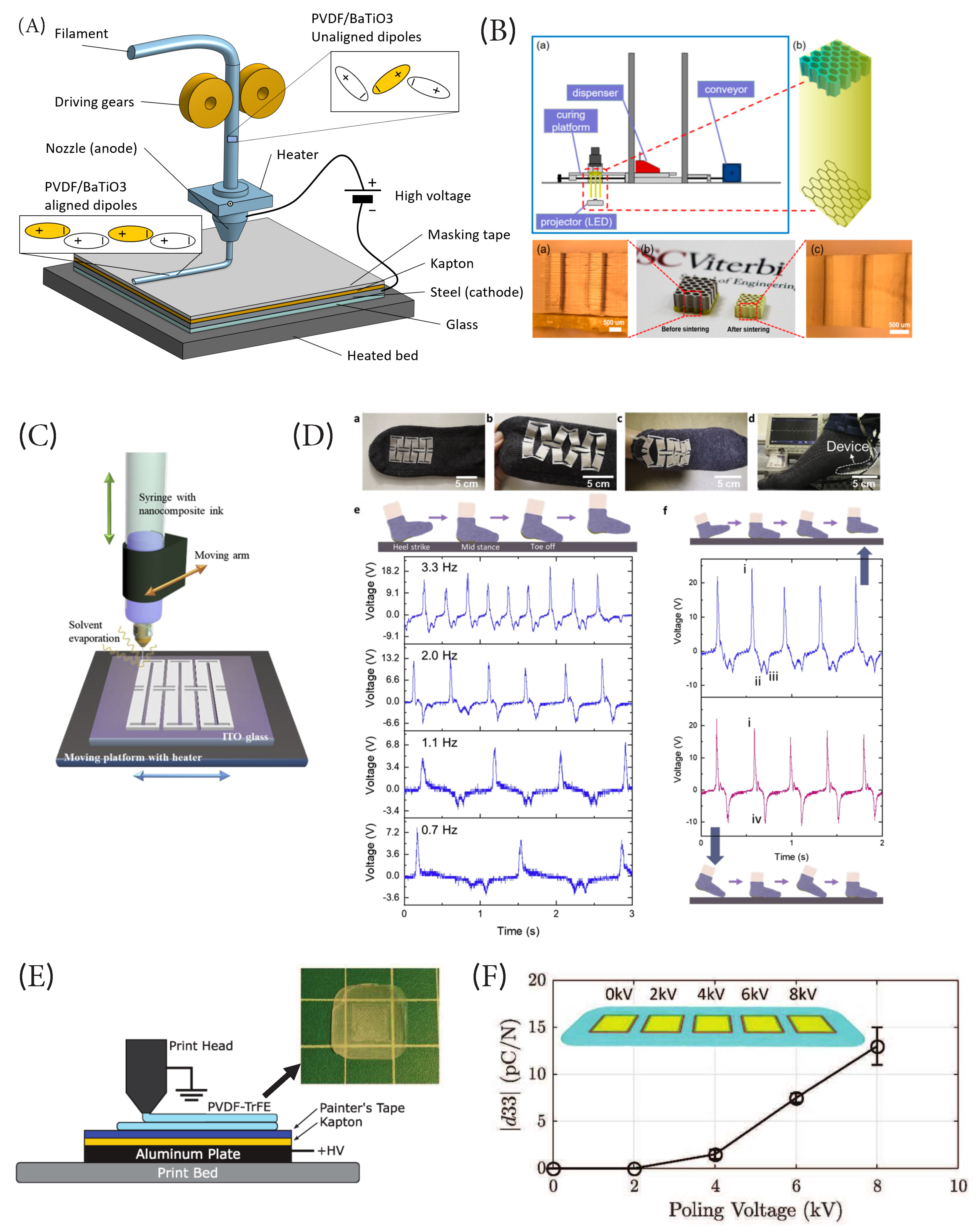
5. 3D Printed Materials

The wide variety of materials suitable for 3DP includes polymers, ceramics, concrete, organic compounds, liquid solutions, composite and metals. Fused deposition modelling (FDM), stereolithography (SLA) and selective laser sintering (SLS) are the most popular techniques well adapted to polymers with resolution down to tens of micrometers. In the FDM a thermoplastic filament is extruded through a heated nozzle layer by layer to form the wanted geometry. SLA technique consists on layer-by-layer solidification of a liquid photopolymer resin through selective UV light exposure such as UV laser or LED array. SLS is based on selective melting through laser of thermoplastic powder. Direct ink writing (DIW), solvent evaporation-assisted 3D printing (SEA-3DP) and pressure assisted micro-syringe (PAM) are suitable for high viscosity ink and fluids, line to layer and then layer by layer. They consist on deposition of an ink, semi-liquid or paste that is subsequently dried or exposed to curing agent under controlled conditions. A similar technique is the Inkjet (IJ) printing, whereby an array of nozzles deposit a low viscosity ink which then solidify forming one layer at a time. Selective laser melting (SLM) and binder jetting (BJ) are particularly suitable for metals where a micro- or nano-powder of the material is selectively fused by a laser to form the desired shape. A comprehensive review of materials and methods of 3DP technologies is beyond the aim of this section and it can be found in [210]. In addition, novel 3DP manufacturing methods such as two-photon polymerization (TPP) and projection micro stereolithography (PµSLA) are capable of micro and nanoscale resolution as discussed by Vaezi et al. [211]. In the field of smart materials [212], a growing number of research efforts are being focused on piezoelectric ceramic materials and electroactive polymers (EAPs) suitable for 3D printing [213]. Comprehensive reviews on this specific topic and on smart materials can be found in [214,215].
In this section, we will summarize some recent relevant innovations regarding piezoceramic composites and piezoelectric polymers about the synthesis and functionalization mainly devoted to mechanical energy harvesting systems. Figure 3 shows a schematic view of the additive manufacturing techniques and materials for mechanical energy harvesters with some examples.

5.1. Piezoceramic Composites

Piezoelectric materials are in general preferred to electromagnetic and electrostatic ones for their high mechanical-to-electrical energy conversion efficiency and ease of device integration. As we have showed in Section 2, piezoceramic materials for mechanical energy harvesting include polycrystalline (PZT, PMN-PT, KNN, BaTiO 3 , LiNbO 3 ) that need poling but also self-poled single crystal ceramics such as quartz and ZnO. Conventional manufacturing techniques for bulk and multilayered piezoceramics include sintering [214,216], powder injection molding [217] and compaction, while for planar structures, solution deposition techniques are commonly used, such as vacuum evaporation, sputtering and laser ablation. Bottom-up techniques such as hydrothermal synthesis are often used for micro and nano-crystals grow like ZnO [218,219], BaTiO 3 and PMN-PT nanowires [220]. All these traditional techniques are mostly limited to 2D geometries such as discs, plates and films that need to be cut in suitable geometries and glued with electrodes. These kind of approaches carry many disadvantages such as high number of process steps, high cost facilities, waste of materials,a difficulties to create complex structures and devices. In addition, the manipulation of dielectric and compliance tensor is pretty much limited in common production process of bulk and laminated piezoceramic and their electromechanical conversion efficiency depends on the symmetry level of their cell lattice structures and chemical composition. Moreover, the bonding of the piezoceramic material with a substrate of metal electrodes results in a higher stiffness that limits the mechanical functionality.
Additive manufacturing of piezoelectric materials open a third-dimension in making piezoelectric generators and allow an incomparable freedom of design, the manipulation of elasticity and amplify the electromechanical coupling also combining 2D planar with 3D out of plane. Nevertheless, not all the fabrication process of a mechanical energy harvester can be done in just one step via 3DP but it needs the poling of the material, electrode formation and integration with electronic interface. In order to reduce the fabrication steps some 3DP techniques performs in situ material poling during the extrusion such as the electrical poling-assisted additive manufacturing (EPAM) [113,221]. The majority of the piezoelectric ceramic are made of polycristalline nanoparticles uniformly dispersed in a thermoplastic, photopolymer or ink suspension used as supporting material that can then processed in one of the 3DP technology described before. Figure 4 shows a mosaic of some relevant examples of 3D printed piezoelectric materials and methods also suitable for energy harvesting applications.
Nanocomposite piezoceramics based on Barium Titanate (BT) nanoparticles (100 nm) mixed with β -PVDF were proposed by several research groups. Kim et al. [113,222] shown the possibility to enhance homogeneous dispersion of BaTiO 3 nanoparticles in PVDF matrix using fused deposition modeling (FDM), while Castels et al. [109] used a support matrix of ABS. All these approaches with FDM technology perform the electrical poling during the filament extrusion. Piezoelectric ceramics can be also prepared with SLA process starting from powder mixed with ball-milling or magnetic stirring with UV photosensitive resin. The 3D printed part is subsequently subjected to debinding process and then sintering at high temperature (usually around 1300 °C). These two densification steps result in a final shrinkage of the object; therefore, the design must be done properly. Chen at al. [102] reported a 3D printed piezoelectric microstructure based on BT with d 33 =160 pC/N for ultrasonic sensing. In addition, Zeng et al. [103] realized a BT-based piezoelectric ceramics with honeycomb structure for ultrasound sensing. Zhou et al. [106] proposed a stretchable piezoelectric nanogenerator with kirigami shape based on BT nanoparticles and (P(VDF-TrFE)) ink printed with DIW technique. Other structures based the same approach were also fabricated with PAM technique by Kim et al. [101], or with BJ [104], SLS [111] and SEA-3DP techniques [223]. There are other research groups that have proposed SLA process for producing high coupling piezoceramics such as PZT [120], PMN-PT [118] and KNN [121].
Another example of the huge potentiality in manufacturing complex three-dimensional architectures of PZT nanocomposites is shown by Cui et al. [224]. In this work, a piezoelectric metamaterial has been realized with the possibility to control the voltage response direction at a given applied stress.

5.2. Piezoelectric Polymers

Piezoelectric polymers are here intended not mixed with ceramics are object of a growing interest because of their flexibility, possibility to get good conversion performance and ease of fabrication. The most widely used pure piezoelectric polymers in 3D printing are PVDF and co-polymers such as P(VDF-TrFE). A PVDF piezoelectric generator for harvesting energy from walking people was proposed by Gao et al. [225]. In this case, a triple-layer PVDF structure array printed with SLA achieved up to 8.6 mW output power during running. Yuan et al. [107] realized a 3D printed ball-structured energy harvester with multilayer β -phase PVDF-TrFE copolymer, obtaining high piezoelectric coefficient ( d 33 ∼130 pC/N) by using a custom DIW technique. Kim et al. [113,226] fabricated piezoelectric films from polyvinylidene fluoride (PVDF) polymer by using FDM 3D printing integrated with corona poling. Lee et al. [221] and Ikei et al. [114] used a similar method called EPAM by combining FDM and electric field generated by electric potential between the nozzle and the build plate so to provide dipoles alignment and produce the β phase crystalline structure of the PVDF. Another way to produce high coupling PVDF for energy harvesting was proposed by Fuh et al. [123] through near-field electrospinning (NFES) technique. In this work, the authors created a 3D printed sinusoidal wavy architecture combined with highly aligned PVDF micro/nano fibers produced by NFES for self-powered foot pressure mapping sensor.
Alternative to PVDF, there also other electroactive polymers that were proposed for 3DP. Chakraborty et al. [227] worked with acrylate printed with SLA, showing that its longitudinal piezoelectric coupling coefficient can be doubled by applying an electric field of 2400 V/m. Polylactic acid (PLA) and poly-L-lactic acid (PLLA) are the most used material in FDM 3D printing and interesting alternatives to petroleum-based polymers. They are biocompatible, biodegradable, renewable and ease of fabrication. Zhao et al. [228] realized a piezoelectric generator by bonding a double layer of thermally treated PLLA and a thick layer of polyethylene terephthalate (PET) used as a substrate layer. The PLLA material showed a shear mode d 14 piezoelectric coefficient of 9.57 pC/N and a the harvester generated a power of 14.45 μ W. However, they did not use a 3D printing method but solvent casting procedure. Mirkowska et al. [116] combined a 3D printed PLA mesh layer with polypropylene (PP) electret foil and elastomer. A very interesting piezoelectric coefficient d 33 resulted from this structure at the level of 300 pC/N. Table 5 shows a comparison of the piezoelectric coefficients of materials only produced with various 3D printing methods here cited.

6. Low Dimensional Materials

In this section, we present recent advancements on piezoelectric low-dimensional material and their applications to energy harvesting, from the fundamental origin of the effect to their application to mechanical energy harvesting. Most of the materials present in this section refers to the class of semiconductors and metals such as transition metal dichalcogenides (TMDs), group-II oxides and III-V compounds. We will start from two-dimensional (2D) materials to one-dimensional (1D) materials such as nanotubes, nanorods and nanowires. The interest of this class of devices it is not limited to energy harvesting applications but it exhibits great potential for nano-scale electromechanical actuators and electronic devices.

6.1. 2D Materials

Two dimensional materials reefers to the class of crystalline solids composed of a single layer of atoms. Among others, the most common and widely know is Graphene, a crystalline allotrope of carbon. From its first experimental characterization in 2004, hundred of new 2D materials have been discovered and experimentally realized in laboratory. 2D materials are not limited to allotropes of a single element but can consist of a compound of two ore more covalently bonding elements. Furthermore, single layers of 2D materials can be staked forming a thin film of homogeneous material or heterostructures bounded by van der Waals forces. While 2D crystalline allotropes have a neutral charge distribution, multiple elements compound can exhibit non-centrosymmetric structure and associated polarization. As in bulk material a deformation can effect the polarization of the structure, coupling the mechanical and electrical behaviors, giving origin to piezoelectric effect with piezocoefficient magnitudes on par with those of wurtzite structure crystals [229].
Interestingly some bulk materials are centrosymmetric in their three-dimensional form, but when stripped down to single or few atomic layers they exhibit piezoelectricity. This effect is due to the fact that the layering of the material cancel out the charge asymmetries. Example of a material exhibiting this effect is hexagonal Boron-Nitride (h-BN). In Figure 5 we present the structure of (h-BN) in its pristine (left panel) and stressed configurations (central and right panels). In its hexagonal configuration boron and nitrogen atoms are covalent bonded in a honeycomb lattice, similarly as graphene, where both atoms species lie in the same plane. While in graphene both atom species are identical, preserving the inversion symmetry, in h-BN the presence of different elements produces a variation of the polarization upon compression or elongation.
In Figure 5 central and right panel we present the change in polarization of a six-atom unit-cell of h-BN under tension and compression. Under tensile stress, the lateral B and N atoms gets away from each other but the lateral polarization remain the same, while top and bottom N and B atom get closer provoking a change in polarization. A similar effect is present upon compression where the top and bottom N and B atoms, respectively, move away from each other, generating a change in polarization in the opposite direction with respect to elongation.
It is interesting to notice that multi-layer h-BN is formed by staking single layers of h-BN weakly bonded by van der Waals forces. The staking of multiple layers could happen in five different ways [230]. Among these the most common is the AA’ staking, where the cells of each layers shares the same atomic coordinates and each layers is rotated by 60° [230,231,232,233,234]). In a two layers configuration the results is a staking where in the second layer the B atoms are replaced by N atoms and vice versa. In this configuration the polarization effect due to the elongation or compression of the first layer is thus canceled by the one in the second layer. The structure is thus no more piezoelectric. Adding another layer piezoelectricity is then restored, where two layers cancel out and only one layers contributes to the piezoelectric effect. This effect can be iterated for an arbitrary number of layers, where structure with odd number of layers are piezoelectric while even ones are not. We should note however that, since only one layers contributes to the piezoelectricity in odd layers structures, while the volume increases and the polarization remain the same the overall effects decreases. For this reason bulk h-BN is considered non piezoelectric.
While two-layers h-BN have no piezoelectric response to tensile strain it has been reported to exhibit piezoelectricity on bending. When an initially flat AA’ odd-layers deforms, small deviations from the ideal AA’ arrangement occurs, generating a variation of the polarization [235].
Similar effect have been theorized and observed in non pure 2D structure, where a single layer is formed by a sandwich of two materials like in transition metal dichalcogenides. In these structure one layer of transition metal atoms (Mo, W, etc.) is sandwiched between two layers of chalcogen atoms (S, Se or Te). In a single layer the atoms are covalent bonded while multiple layers are bonded via van del Waals forces. Most common TMD are MoS 2 , WS 2 , MoSe 2 , WSe 2 , MoTe 2 . These monolayers are semiconductors with a direct band-gap, and have been studied for use in electronic and optical applications [236,237,238,239,240].
Like in pure 2D crystals, TMD can show piezoelectric effect due to the different atomic species composing the crystal. Depending on the staking of multiple layers the piezoelectric effect could be cancelled out. For sake of discussion in Figure 6 we present the structure of MoS 2 in its single layer 2H phase (left panel) along with the most common staking in top-to-tail configuration (right panel), where the cell of the second layer are shifted along the x direction and represented faded in figure. The piezoelectric axis of each monolayer is opposed to its adjacent ones; therefore, for even number of layers the piezoelectric effect is zero. For an odd number of layer each even number of layer cancel out and the global remnant piezoelectric effect is thus negligible for more than a small odd number of monolayers [241].
The large surface energy of atomically thin material can cause piezoelectric structures to be thermodynamically unstable [242]. Transition-metal dichalcogenides can retain their atomic structures down to the single-layer limit without lattice reconstruction [243], even under ambient conditions and thus are more suitable, from a structural point of view, for realizing 2D energy harvester.
Bidimensional material have only a non-zero d 11 coefficient. However, TDMs, when buckled can exhibit also d 31 coefficients [244]. Piezoelectric coefficient for 2D material have been reported to be in the range 1–10 pC/N from experiments and numerical studies, in Table 6 we summarize the values for most common 2D materials [229,244,245,246,247].
Several application of two-dimensional piezoelectric nanomaterial for energy harvesting have been proposed in the past few years [125,128,133,136,137,138,140,141,143,144,248]. The advantages with respect to their bulk counterpart are their enhanced flexibility and ability to sustain large strain and deformation. For this reason these material are good candidates in large strain environments, such as human activities. However, some 2D material have been demonstrated mild to severe toxicity [249,250,251]. In Ref. [128] authors provide a comprehensive review of recent advances in 2D material based wearable energy sources. 2D materials can also be used as additional piezoelectric layer to non-piezoelectric substrate. In Ref. [125] the authors computationally study the electrical response of layered 2D nanosheets (h-BN, MoS 2 , MoSe 2 , MoTe 2 , WS 2 , WSe 2 , and WTe 2 ) deposited on a silicon substrate to form cantilever energy harvesters. The authors estimate an output power up to 1.4 nW for MoTe 2 . Another study of dynamical energy harvesting from a h-BN monolayers is presented in Ref. [140], where the authors exploit non-linearity to enhance the dynamical, and thus electrical, response of a nanoscale energy harvester. The authors show that a 20 nm × 1 nm h-BN monolayer, under a compressive strain ε = 0.3% can harvest up to 0.18 pW from a 5 pN vibration.

6.2. 1D Materials

When it comes to convert energy from tinny mechanical deformations, as such produced by vibrations on mechanical structures, to the electrical to downscale has revealed to be a very efficient strategy to maximize the device performance in terms of harvested power density by unit of input energy [252]. Following this indication, it seems reasonably to spend some efforts exploring the performance of devices based on One-dimensional (1D) materials. These refer to nanostructured materials with lengths superior to 100 nanometers only along one dimension. The possibilities regarding their particular shape, morphology and composition are multiple, including nanowires, nanorods and nanotubes. Other kinds of 1D systems are molecular chains [253,254] or those emerging from the creation of a physical interface when two low dimensional materials are put in contact. Despite having extremely interesting properties promising for energy related applications as well [255,256,257,258], will not be treated in this review. In this section, the most promising approaches and results regarding nanoegenerators based on 1D mateirals and, in particular, those implementations in which mechanical deformations are the main source of energy. Again, the piezoelectric properties of some materials reveal as extremely appealing for such propose. In fact larger piezoelectric coefficients and attainable deformations of nanoscale piezoelectic materials lead to an improvement of the mechanical to electrical energy conversion efficiency.
There are mainly two functioning modes based on the piezoelectric response of a 1D system, namely compressing/stretching mode and bending mode, which are schematically represented in Figure 7 panels (a) and (b), respectively.
Generally, this effect can be effectively exploited in nanowires (NW), rods and nanotubes (NT) since these structures can withstand great mechanical stresses. Among the most used structures for energy harvesting applications we find those based on the so-called third generation of semiconducting materials such as GaN [259,260], InN [261], InAs [262], CdS [263], CdTe [264] and ZnO [146,256,265,266,267], the latter being one of the most used an promising candidates for large-scale production as discussed below. These materials having non-centrosymmetric crystal structures have piezoelectric properties along their c-axis most being wurtzitic materials. For ZnO, the piezoelectric constant d 33 has been reported to fall in the range of 12 pm/V. The first study linking 1D ZnO with energy harvesting was reported by Z. L. Wang et al., in 2006 [266], wherein aligned ZnO NW arrays converted mechanical energy into electric power. In this case, the conversion mechanism was a combination of the modulation of the piezoelectric potential due to the charge separation in the body of the active material (see Figure 7c) coupled to the formation of a Schottky barrier between the metal leads and the NW, as depicted in Figure 7d.
Besides these materials, PZT, a widely used family of piezoelectric ceramic materials with high piezoelectric voltage and dielectric constants, have ideal properties for mechanical to electrical energy conversion. Generally, PZT can generate much higher voltage and power outputs than the piezoelectric materials named above, but it suffers from low flexibility. While bulk and thin film PZT structures and related materials are extremely fragile, their 1D counterparts showing high length to radius ratios can improve mechanical flexibility [268] as reported for Pb(Zr,Ti)O 3 NWs [146], BaTiO 3 NWs [41,269] and SbN BiN NWs [270], reporting output voltages in the order of 1 V and current densities of the order of 1 μ A/cm 2 . A proof of the outstanding performance 1D systems is a proof-of-concept device composed by vertically aligned Pb(Zr0.522Ti0.48)O 3 NWs that reported output voltages as high as 209 V [148]. For BaTiO 3 NTs, with perovskite structure, output voltages of up to 5.5 V have been reported under a stress of 1 MPa demonstrating high mechanical flexibility and enhanced piezoelectric coefficient [271] with respect to ZnO NWs, while PbTiO 3 NT composites have demonstrated output voltages of 0.6 V under bending and an output current densities of 1 nA cm 2 [150].
While the performance of the aforementioned proof-of-concept realizations are encouraging, we still need a cost-effective device supporting high output powers by using easily accessible and nontoxic 1D materials as lead-free ones [272,273]. Moreover, most of the best performing materials require a calcination process to fall in its ferroelectric phase. The high Curie temperatures of these materials prevent its use for flexible electronics since flexible substrates tend to loose their elasticity after a calcination processes. Again, the synthesis of large quantities of ZnO can be obtained efficiently without the need of high temperatures.
Nanofibers are closely related to nanowires and nanotubes, the main difference being the presence of defects along their length. Given the dimensions of these structures counting with diameter to length ratios in the order of 10 3 , the use of nanofibers for energy harvesting technology could effectively provide portable, flexible and efficient energy harvesting devices with enhanced low-frequency response: nanofibers exhibit very high bending flexibility and high mechanical strength and, in some cases, very high piezoelectric voltage constants as in PZT nanofibers (g 33 = 0.079 Vm/N) [274]. These can be finely arranged to form dense arrays of laterally aligned PZT nanofibers [275].
Other interesting materials capable of presenting a high piezoelectric response are represented by composites. One of them is the NaNbO 3 nanowire PDMS polymer composite, with which up to 3.2 V has been obtained [152], or more sophisticated methods to activate composite materials being simple, low-cost and prone to large-area fabrication based on carbon NTs decorated with BaTiO 3 nanoparticles to produce an efficient piezoelectric nanocomposites [153].
In Table 7, we summarize the reported voltages and current densities for significant 1D material nano-generators. Notice that, while piezoelectric constants for 2D materials that we reported in Table 6 can be directly compared, voltages and output currents strongly depend on how the device is excited. As said before, an enhancement of the electro-mechanical coupling is expected for nanoscale materials. In addition to this another advantage arise at the nanoscale: the generation of a macroscopic polarization caused by a strain gradient or, more generally, by inhomogenous strain distributions, namely the flexoelectric effect [276,277]. Flexoelectricity, which is common to all semiconducting materials, adds a new component to the charge separation mechanism that might be insignificant for bulk materials but increasingly important when going nano and, in particular, is expected to boost the response of 1D materials [267]. Therefore, taking advantage of the flexoeletric component of the materials response by proper design can increase significantly the harvested power of a nanogenerator, as demonstrated in [278] with PZT grown on carbon NTs.

7. Conclusions

In this work, we discussed several piezoelectric materials and their applications for mechanical energy harvesting. Eco-friendly and biodegradable solutions are getting more important with the advent of mass-scale production of sensors for the IoT; thus, the sustainability of energy harvesters is a key aspect to their implementation and commercialization. Moreover, specific applications, such as wearable or implantable devices for drug delivery, require the use of materials that are non-toxic and biocompatible. It is also important to consider their cost and their abundance in the environment in order to implement sustainable solutions. Lead-free materials represent a good opportunity to meet these expectations, not only as a valid alternative of Pb-based ceramics, but they could also improve present and future energy harvesting solutions. For instance, it has been shown that some materials (AlN, BFO, LN, KNN, and ZnO) can be implemented in CMOS process, and therefore they could be implemented for industrial upscaling of MEMS devices. In terms of electromechanical properties, commercial availability and high temperature resistance AlN, LN and KNN represent already an alternative to Pb-based ceramics for vibrational energy harvesting. The latter has an electromechanical coupling coefficient of 0.12–0.49 compared to 0.44 of the former. Polymers such as PVDF, and nanogenerators based on BT, BFO and ZnO can be used wherever flexibility or direct deformation are important, and hence for wearable applications, whereas EAPap and biodegradable bacterial-based cellulose could improve the sustainability of sensor needed in the environment and reduce their footprint. With reference to 3D printing methods, BT based nanomaterials, KNN, PVDF-TrFE and Polypropylene show at the same time high design flexibility, good mechanical properties, low cost and biocompatibility, although lower piezoelectric coefficients than PZT and PMNT based structures. Further innovative materials, such as organic materials and 2D crystals, are still not directly comparable to mature solutions due to lack of studies. While some of them show promising piezoelectric coefficients, their effectiveness in energy harvesting solutions should be assessed also in terms of electro-mechanical coupling and their scalability.

Author Contributions

All authors contributed equally to this work. All authors have read and agreed to the published version of the manuscript.

Funding

This research was partially funded by the EU Horizon 2020 research and innovation programme, under Grant Agreement n. 730957.

Data Availability Statement

All supporting data are presented in the manuscript and listed references.

Conflicts of Interest

The authors declare no conflict of interest.

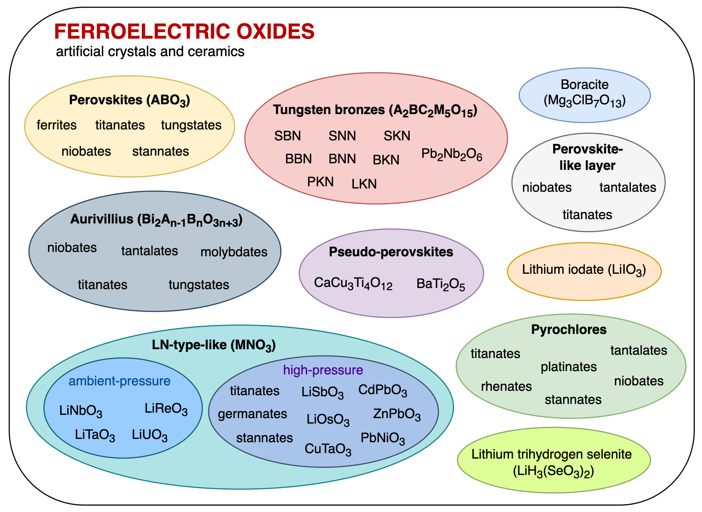
Appendix A. Piezoelectric Materials Zoo

The following section represents a summary on the many classes of piezoelectric materials that have been studied over the years. We present their crystal structures and properties, along with their composition and fabrication methods. Piezoelectric materials can be broadly categorized in five main classes: ferroelectric oxides, non-ferroelectric oxides, salts, 2D/3D semiconductors and metals and organic materials.

Appendix A.1. Ferroelectric Oxides

This class includes many synthetic crystals and ceramics. One of the most commonly used piezoelectric ceramic with an high energy conversion gain and extensively used in industries is Pb[Zr x Ti 1 x ]O 3 (PZT) that is based on the perovskite structure ABO 3 , where A and B sites are occupied by alkaline/alkaline earth or transition metal ions and the A atom is usually bigger than the B. This structure also describes such compounds such as BaTiO 3 (BTO), [K x Na 1 x ]NbO 3 (KNN), BiFeO 3 (BFO), NaWO 3 (NWO) [279]. Starting from this structure, others can be obtained: the pseudo-perovskite structures such as BaTi 2 O 5 , grown from BTO with a TiO 2 eccess through the Linz method [280], the perovskite-like layered structure (PLS) A 2 B 2 O 7 consisting of tilted BO 6 octahedra sharing corners with each other and A ions filling the space between them, such as La 2 Ti 2 O 7 or Sr 2 Nb 2 O 7 [279,281,282]; the pyrochlore structure, with the same chemical formula of PLS but where groups of six BO 6 octahedra sharing their corners surround an eight coordination of the B cation, such as Eu 2 Ti 2 O 7 or Sm 2 Nb 2 O 7 [283] (these two compounds crystallize in the PLS structure at high pressure, although at ambient pressure they crystallize in the pyrochlore structure) and the Aurivillius phase or bismuth layer structured ferroelectrics (BLSF) Bi 2 A n 1 B n O 3 n + 3 where A is a mono-, bi- or trivalent ion in a dodecahedral coordination and B is a cation in an octahedral coordination, consisting in n pseudo-perovskite layers (A n 1 B n O 3 n + 3 ) 2 alternating with [Bi 2 O 2 ] 2 + layers (n can range from 1 to , for which the repeated cell is the pure perovskite), such as Bi 2 WO 6 (n = 1), Bi 2 SrNb 2 O 9 (n = 2), Bi 4 Ti 3 O 12 (n = 3) and Bi 4 CaTi 4 O 15 (n = 4) [279,284]. The tetragonal tungsten-bronze structure (TTB) A 2 BC 2 M 5 O 15 involves large cations (Ba 2 + , Pb 2 + ) occupying the A and B sites, small low charged cations (Li + ) in the C sites and small high charged cations (Nb 5 + , Ta 5 + ) in the M sites, it consists in a multi-tunnel structure of rings formed by four or five MO 6 octahedra sharing their corners and alternating ions filling the space in the tunnels and describes compounds such as Sr 2 NaNb 5 O 15 (SNN), Sr x Ba 1 x Nb 5 O 15 (SBN), Li 2 K 3 Nb 5 O 15 (LKN) and PbNb 2 O 6 [279,285]. The LN-type structure MNO 3 with point group 3 m , comes from an alteration of the ilmenite structure FeTiO 3 (in turn, a corundum superstructure) where the M and N ions fill singularly distorted oxygen octahedra sharing their edges and faces but only two-thirds of the geometric structure, leaving a vacancy and with the following sequence:
Li , _ , Nb , Li , _ , Nb , . . .
This absence breaks the simmetry of the hexagonal close packing (hcp) and this structure describes compounds such as LiNbO 3 , LiTaO 3 [286], LiReO 3 [287] and LiUO 3 at ambient pressure and LiSbO 3 [288], MgTiO 3 , ZnSnO 3 [289], FeGeO 3 and CdPbO 3 at high pressure [290]. Figure A1 presents materials of this class divided by sub-classes.
Figure A1. The class of ferroelectric oxides consisting in perovskites, tungsten bronzes, perovskite-like layer, pyrochlores, Aurivillius phase and LN-type-like materials.
Energies 15 06227 g0a1

Appendix A.2. Quartz and Non-Ferroelectric Oxides

This class features both natural and synthetic crystals. The leading hard crystalline mineral of this group, used in oscillators, resonators and filters is quartz (SiO 2 ), a three-dimensional covalent network compound containing Si-O covalent bonds which form SiO 4 tetrahedra, sharing two of their four corners with each other in a three-fold or six-fold helical chain that run parallel to the c axis [291]. It can exist as two polymorphic forms: α -quartz with point group 32, stable at room temperature and pressure and β -quartz with point group 622, stable at temperature above 573 °C [279]. Other crystals, called quartz analogues or quartz-like with MNO 4 structure, belonging to the same 32 crystallographic point group are GeO 2 [292] (identical to quartz, since germanium belongs to the same group IV of silicon), berlinite (AlPO 4 ), other phosphates such as GaPO 4 [293], FePO 4 or BPO 4 and arseniates such as GaAsO 4 [279], AlAsO 4 and FeAsO 4 , which have the same structure of quartz but where the SiO 4 tetrahedra are replaced by alternating MO 4 and NO 4 tetrahedra (this configuration doubles the magnitude of the piezoelectric effect) [291]. The langasite structure A 3 BC 3 D 2 O 14 with point group 32, where the A cation is in a decahedral coordination, the B cation in an octahedral coordination and the C and D cations in a tetrahedral coordination, describes ordered crystals such as langasite (La 3 Ga 5 SiO 14 ), langatite (La 3 Ga 5.5 Ta 0.5 O 14 ), langanite (La 3 Ga 5.5 Nb 0.5 O 14 ) [294] and Ca 3 TaAl 3 Si 2 O 14 (CTAS) [295] or more disordered crystals such as Ca 3 Ga 2 Ge 4 O 14 (CGG), Sr 3 Ga 2 Ge 4 O 14 (SGG) [296] and La 3 SbZn 3 Ge 2 O 14 (LSZG) which possess higher piezoelectric coefficients than the ordered structures [279]. The sillenite structure Bi 12 MO 20 with point group 23, where the possible metal ions M=Si, Ge, Ti occupy oxygen tetrahedra and the bismuth ions are in an eight oxygen atoms coordination, describes the Bi 12 SiO 20 (sillénite mineral), Bi 12 GeO 20 and Bi 12 TiO 20 crystals [297]. The oxyborate structure (ReCOB) ReCa 4 O(BO 3 ) 3 with point group m, where Re stands for the series of rare-earth elements (scandium, yttrium and lanthanides), consists of skewed CaO 6 and ReO 6 octahedra and (BO 3 ) 3 trigonal planar groups linked together at the corners and describes compounds such as ScCa 4 O(BO 3 ) 3 , YCa 4 O(BO 3 ) 3 , LaCa 4 O(BO 3 ) 3 , NdCa 4 O(BO 3 ) 3 and PrCa 4 O(BO 3 ) 3 [279,298]. A promising material used for bulk acoustic wave (BAW) and surface acoustic wave (SAW) filters is lithium tetraborate (Li 2 B 4 O 7 ) with point group 4 m m , formed by two BO 3 trigonal planar groups and two BO 4 tetrahedral groups sharing their corners and lithium ions in a tetrahedral coordination which share corners and edges with them [279,299]. Figure A2 presents materials of this class divided by sub-classes.
Figure A2. The class of quartz and non-ferroelectric oxides including langasites, sillenites, wurtzites, zinc-blendes and oxyborates.
Energies 15 06227 g0a2

Appendix A.3. Salts

This class features both natural and synthetic crystalline salts. The family of tartrates, based on the content of the salt dianion C 4 H 4 O 6 2 of tartaric acid includes Rochelle salt (KNaC 4 H 4 O 6 ) with point group 222, one of the first piezoelectric materials discovered by Pierre Seignette in 1675 and extensively used in microphones, transducers and electronics, where K + and Na + ions are ionically bonded to tartrate [300,301]. Other compounds included in this group are the potassium salt of tartaric acid K 2 C 4 H 4 O 6 (DKT) where two K + ions are bound [301], the cadmium salt CdC 4 H 4 O 6 where a Cd 2 + is bound [302], the ammonium salt (NH 4 ) 2 C 4 H 4 O 6 (DNT) where two NH 4 + cations are bonded and the ethylenediamine salt C 2 H 4 (NH 3 ) 2 C 4 H 4 O 6 (EDT) with point group 2, which forms a monoclinic crystal structure [300,303]. The group of ferroelectric salts features struvite (MgNH 4 PO 4 ·6H 2 O) with point group m m 2 , a magnesium ammonium hydrate phosphate where octahedral [Mg(H 2 O) 6 ] 2 + coordination complexes are connected to NH 4 + and PO 4 3 tetrahedra through hydrogen bonds and which forms orthorhombic crystalline structures [304] and triglycines, namely the sulfate (NH 2 CH 2 COOH) 3 H 2 SO 4 (TGS) [300,301], the selenate (NH 2 CH 2 COOH) 3 H 2 SeO 4 (TGSe) and the tetrafluoroberyllate (NH 2 CH 2 COOH) 3 H 2 BeF 4 (TGFB), the structure of which consists in SO 4 2 , SeO 4 2 or BeF 4 2 tetrahedra held together by hydrogen bonds to three glycine species. The group of paraelectric salts contains another early material discovered to exhibit piezoelectricity, that is monopotassium phosphate KH 2 PO 4 (KDP) which becomes ferroelectric at temperatures below −150 °C [300]. Other similar compounds are KH 2 AsO 4 (KDA), where the phosphate anion is replaced by the arsenate anion, NH 4 H 2 PO 4 (ADP) [300] and NH 4 H 2 AsO 4 (ADA), where the potassium ion is replaced by the ammonium cation. The epsomite structure with point group 222, which takes its name from the homonymous mineral with chemical formula MgSO 4 ·7H 2 O (Epsom salt), consists in SO 4 2 tetrahedra and octahedral [Mg(H 2 O) 6 ] 2 + coordination complexes connected by hydrogen bonds, it forms a disphenoidal orthorhombic crystal structure [305] and describes also two other salts: Goslar salt or goslarite (ZnSO 4 ·7H 2 O), strongly diamagnetic and morenosite (NiSO 4 ·7H 2 O). Some other inorganic salts that possess piezoelectric properties are lithium sulfate monohydrate (Li 2 SO 4 ·H 2 O) [306], nickel sulfate exahydrate (NiSO 4 ·6H 2 O), sodium chlorate (NaClO 3 ) and sodium bromate (NaBrO 3 ), where these last compounds consist in ClO 3 /BrO 3 trigonal planar groups which bind the sodium ions [307]. Figure A3 presents materials of this class divided by sub-classes.
Figure A3. The class of salts including tartrates, epsomites, salammoniac, ferroelectric, paraelectric and inorganic salts.
Energies 15 06227 g0a3

Appendix A.4. Semiconductors and Metals

This class includes both three-dimensional bulk materials and two-dimensional compounds. One of the most relevant family known for its piezoelectric properties is that of II-VI group and III-V group semiconductors (AB structure), consisting in metal binary compounds, where the first is composed by an element of group 12 (Zn, Cd, Hg) and a chalcogen of group 16 (O, S, Se, Te) while the second is composed by an element of group 13 (B, Al, Ga, In) and a pnictogen of group 15 (N, P, As, Sb) [308]. Some of this compounds possess the hexagonal wurtzite structure with point group 6 m m , while others possess the cubic zincblende structure with point group 4 ¯ 3 m [309]. Binary zincblende structures are piezoelectric because there is a coupling between the macroscopic strain and the microscopic one (the linear macroscopic piezoelectric tensor is decomposed in an purely electronic term and an intrinsic strain term) of opposite sign, leading to a weak but still present piezoelectric effect. Some wurtzite-like compounds from II-VI group are zinc oxide (ZnO), occurring in nature as the zincite mineral [310], zinc sulfide (ZnS), present in the sphalerite mineral and cadmium sulfide (CdS), occurring in nature as the rare greenockite and hawleyite minerals [311], while from III-V group are aluminium nitride (AlN) [279], gallium nitride (GaN), a wide-bandgap semiconductor [279,312] and indium nitride (InN), a narrow-bandgap semiconductor. Some zincblende-like compounds from II-VI group are zinc selenide (ZnSe), a wide-bandgap semiconductor rarely occurring in nature as the stilleite mineral and also crystallizing in wurtzite structure [313], mercury sulfide (HgS), occurring in nature as the black metacinnabar ( β -HgS) mineral and cadmium telluride (CdTe), used for electro-optic modulators and photovoltaic applications e.g., thin film solar cells [314], while from III-V group are boron phosphide (BP), gallium arsenide (GaAs), a direct bandgap semiconductor used for transistors and solar cells [315], indium antimonide (InSb), a narrow-bandgap semiconductor used for infrared detectors [316]. Adding a different species of atoms in the wurtzite or zincblende structure, a superstructure can be obtained. The wurtzite superstructure describes compounds such as enargite (Cu 3 AsS 4 ), a copper arsenic sulfosalt mineral, cubanite (CuFe 2 S 3 ), a copper iron sulfosalt mineral and lithium gallium oxide (LiGaO 2 ), a synthetic crystal [317], while the zincblende superstructure describes minerals such as stannite (Cu 2 FeSnS 4 ), bornite (Cu 5 FeS 4 ) and luzonite (Cu 3 AsS 4 ), a dimorph of enargite and the group of chalcopyrite crystals [318]. These have a MNX 2 structure, where M can be a transition metal (Cu, Ag, Zn, Cd) or an alkaline earth metal (Be, Mg), N a carbon atom, a semimetal (Si, Ge) or a p block metal (Al, Ga, In, Tl, Sn) and X a semimetal (As, Te) or a non-metal (N, P, S, Se), describing compounds such as CuFeS 2 , in which compared to ZnS, the four zinc atoms are replaced by two copper atoms and two iron atoms, doubling the unit cell [319] and others such as CuGaSe 2 , AgInTe 2 , ZnSiP 2 , CdGeAs 2 and BeCN 2 . A wide class of natural minerals exhibits piezoelectric properties depending on the non-centrosymmetric point group to which they belongs [320] and particularly significant are the synthetic crystals of fresnoite group with tetragonal structure and point group 4 m m , that are the silicate Ba 2 TiSi 2 O 8 and the germanate Ba 2 TiGe 2 O 8 [321]. The family of thiohalides with ABX structure, where A is an element from group 15 (Sb, Bi), B is from group 16 (S, Se, Te) and X is a halogen (Cl, Br, I), consists in two pleated (AB) n n + chains tied together by short and strong Sb-S bonds [322] and describes ternary compounds such as antimony sulfoiodide (SbSI), that possesses the highest Curie temperature (T = 295 K), high-volume piezoelectric module (d = 1000 pC/N) and an extremely high electromechanical coupling coefficient (k = 0.90) [323], bismuth sulfochloride (BiSCl) and bismuth selenobromide (BiSeBr) that mainly crystallize in needle-like structure along c-axis due to their anisotropy. The family of metal monochalcogenides (MMCs) with MX structure [324], where M can be a metal of group 13 (Ga, In) or group 14 (Si, Ge, Sn) and X is a chalcogen (S, Se, Te), has a crystal structure isostructural with the orthorhombic one of phosphorene but where M and X atoms are alternate with each other and covalently bonded to three neighbors of the other atomic species, forming a puckered or wavylayer structure of zigzag, along y axis or armchair, along x axis [325]. Symmetrical bulk crystals consists of vertically stacked X–M–M–X layers held together by weak van der Waals-like forces, which lose their inversion symmetry after having exfoliated down to monolayers, making them non-centrosymmetric, and therefore potentially piezoelectric. The most studied compounds are gallium sulfide (GaS), gallium selenide (GaSe) and indium selenide (InSe) from III group [326] and germanim sulfide (GeS) and selenide (GeSe), tin sulfide (SnS) and silicon sulfide (SiS) and selenide (SiSe) from IV group [327]. The family of transition metal dichalchogenides (TMDs) with MX 2 structure, where M is a transition metal (Cr, Mo, W, Nb, Ta, Re, Ti, Zr, Hf) and X is a chalcogen (S, Se, Te), has the same piezoelectric properties of MMCs when reduced from bulk crystals to monolayers [244], which consist of three atomic X–M–X planes of the two species and if viewed from the top, have a honeycomb structure where adjacent sites are occupied by two alternating species [229] and describes compounds such as molybdenum disulfide (MoS 2 ) [127] and diselenide (MoSe 2 ), tungsten disulfide (WS 2 ), niobium diselenide (NbSe 2 ) and tantalum ditelluride (TaTe 2 ) [244]. By controlling the stoichiometric ratio of chemical vapor deposition the M atoms and X chalcogens quantities can be tuned, allowing to have three atomic X-M-Y planes with two different species of chalcogens, obtaining the so called Janus dichalcogenides with MXY structure [328] that describes compounds such as MoSSe, MoSeTe, MoSTe, WSSe, WSeTe and WSTe [329]. Figure A4 presents materials of this class divided by sub-classes.
Figure A4. The class of semiconductors and metals featuring II-VI and III-V group semiconductors, minerals, thiohalides, metal monochalcogenides and transition metal dichalcogenides.
Energies 15 06227 g0a4

Appendix A.5. Organic Materials

This class includes many crystals and semi-crystalline films. Among organic crystals there are sucrose (C 12 H 22 O 11 ), a disaccharide composed of glucose and fructose subunits which forms a twofold molecular chain where the molecules are tightly bound through hydrogen bonds and van der Waals contacts and resulting in an overall polarity maintained at the three-dimensional level [300,330], resorcinol (C 6 H 4 (OH) 2 ), one of the three isomers of benzenediol that forms an orthorhombic crystal structure [301] and benzophenone (Ph 2 CO or (C 6 H 5 ) 2 CO), belonging to the class of aromatic ketones and the orthorhombic crystals of which are grown from acetone and carbon tetrachloride (CCl 4 ) solutions [301]. This category also contains some peptides such as glycine (Gly or C 2 H 5 NO 2 ), a zwitterionic amino acid which crystallizes in a structure of molecular layers linked together by hydrogen bonds ( β -glycine) [331,332], diphenylalanine (FF or C 15 H 15 NO 2 ), a highly biocompatible amino acid consisting of two phenylalanine molecules that can be self-assembled into semi-crystalline peptidic nanotubes and microrods [332,333] and L-alanine (Ala or C 3 H 7 NO 2 ) and L-hydroxyproline (Hyp or C 5 H 9 NO 3 ), which are two of the building blocks of collagen that exhibit piezoelectric properties in their single crystalline form [331]. The family of polymers features three types of them: semi-crystalline polymers, biopolymers and amorphous polymers. The group of semi-crystalline polymers includes the first piezoelectric polymer discovered by Kawai [334] in 1969, that is poly(vinylidene fluoride) (PVDF) featuring interesting physical and chemical properties in the β phase such as compact structure, chemical stability, large permanent electrical dipole moment (due to the large C-F dipole moments), ease of manufacturing and low annealing temperature and recognized as the “ferroelectric polymer” par excellence [332,335,336,337]. In addition of this there are also some of its copolymers as poly(vinylidene fluoride-co-trifluoroethylene) (P(VDF-TrFE)) [332,336,337,338], poly(vinylidenefluoride-co-hexafluoropropene) (P(VDF-HFP)) [336] and poly(vinylidenefluoride-co-chlorotrifluoroethylene) (P(VDF-CTFE)) [336], all obtained through copolymerization, polydimethylsiloxane (PDMS), a transparent, inert, non-toxic and biocompatible compound [339], Nylon-11 (polyamide-11 or PA-11), a bioplastic obtained from the polymerization of 11-aminoundecanoic acid and characterized by an even number of methyelene groups and one amide group resulting in a net dipole moment [336,337,338,340], poly- β -hydroxybutyrate (PHB), a biocompatible material belonging to the class of polyesters and produced by microorganisms [340,341] and the subgroup of polyureas, types of elastomers that exhibits excellent chemical, thermal and organic solvent resistance, consisting of repeating disubstituted urea molecules monomers, formed by the reaction of isocyanates and amines and which can be aromatic, such as P(MDI/MDA), or aliphatic, such as polyurea-5, synthesized at low temperatures [336,337,340]. The group of bioactive polymers, interesting due to their increasing use in biomedical applications, includes natural polypeptides such as poly( γ -benzyl-L-glutamate) (PBG) [333,337] and poly( γ -methyl-L-glutamate) (PMG) [337,340], that generally show poor mechanical, electrical and electromechanical properties, synthetic polymers such as polylactide (PLA), a thermoplastic polyester obtained by condensation of lactic acid with loss of water [332,333,336,337,338,340] and polyglycolide (PGA), a biodegradable polymer obtained from the ring-opening polymerization of glycolic acid [336] and the subgroup of structural polysaccharides [340] such as cellulose, consisting of linear chains of D-glucose units linked by glycosidic bonds β (1-4) forming fibrils with crystalline and amorphous regions, amylose, a starch component with the same chains of D-glucose molecules but linked by glycosidic bonds α (1-4) and chitin, a long-chain polymer of N-acetylglucosamine molecules (GlcNAc) linked by glycosidic bonds β (1-4). The group of amorphous polymers, characterized by lower electroactive properties than semicrystalline polymers but nevertheless with a large dielectric relaxation strenght and the polarization phenomenon in a quasi-stable state, features polyvinyl chloride (PVC), the polymer of vinyl chloride for which the piezoelectric properties can be improved using stretching methods [336,342], polyvinyl acetate (PVAc), the synthetic aliphatic polymer of vinyl acetate [336,340], poly(vinylidene cyanide-co-vinyl acetate) (P(VDCN/VAc)), a copolymer for which the introduction of large dipole moments such as cyanide groups -CN brings out strong piezoelectricity [336,343], polyphenylethernitrile (PPEN), a super-engineering plastic polymer with high melting point and high glass transition temperature [336,344], polyacrylonitrile (PAN), one of the most widely used synthetic thermoplastic polymer [336] and the polyimide ( β -CN)APB/ODPA, containing three polar functional groups and with a net piezoelectric coefficient an order of magnitude lower than PVDF [337,345]. One of the most promising organic material for piezoelectric nanogenerator (PENG) applications due to properties such as medium band gap, water resistivity, chemical stability, reliable thermal endurance, non-toxicity, biocompatibility, super hardness and wear resistance is graphitic carbon nitride (g-C 3 N 4 ), a graphite analogue consisting in a multilayer structure with regularly distributed non-centrosymmetric triangular nanopores (tri-s-triazine sheets), the configuration of which lead to flexoelectricity and in-plane piezoelectricity [346,347]. Figure A5 presents materials of this class divided by sub-classes.
Figure A5. The class of organic materials consisting in organic crystals, biological materials and polymers.
Energies 15 06227 g0a5

References

  1. Spillman, W.B.; Sirkis, J.S.; Gardiner, P.T. Smart materials and structures: What are they? Smart Mater. Struct. 1996, 5, 247–254. [Google Scholar] [CrossRef]
  2. Bogue, R. Smart materials: A review of capabilities and applications. Assem. Autom. 2014, 34, 16–22. [Google Scholar] [CrossRef]
  3. Orfei, F.; Neri, I.; Vocca, H.; Gammaitoni, L. Nonlinear bi-stable vibration energy harvester at work. In Proceedings of the International Design Engineering Technical Conferences and Computers and Information in Engineering Conference, Buffalo, NY, USA, 17–20 August 2014; American Society of Mechanical Engineers: New York, NY, USA, 2014; Volume 46414, p. V008T11A091. [Google Scholar]
  4. Peterson, J.; Lopes, V.; Cunha, A., Jr. On the nonlinear dynamics of a bi-stable piezoelectric energy harvesting device. In Proceedings of the 24th ABCM International Congress of Mechanical Engineering (COBEM 2017), Curitiba, Brazil, 3–8 December 2017. [Google Scholar]
  5. Vocca, H.; Cottone, F.; Neri, I.; Gammaitoni, L. A comparison between nonlinear cantilever and buckled beam for energy harvesting. Eur. Phys. J. Spec. Top. 2013, 222, 1699–1705. [Google Scholar] [CrossRef]
  6. Sharma, P.K.; Baredar, P.V. Analysis on piezoelectric energy harvesting small scale device—A review. J. King Saud-Univ. 2019, 31, 869–877. [Google Scholar] [CrossRef]
  7. Cottone, F.; Mattarelli, M.; Vocca, H.; Gammaitoni, L. Effect of boundary conditions on piezoelectric buckled beams for vibrational noise harvesting. Eur. Phys. J. Spec. Top. 2015, 224, 2855–2866. [Google Scholar] [CrossRef]
  8. Neri, I.; Travasso, F.; Mincigrucci, R.; Vocca, H.; Orfei, F.; Gammaitoni, L. A real vibration database for kinetic energy harvesting application. J. Intell. Mater. Syst. Struct. 2012, 23, 2095–2101. [Google Scholar] [CrossRef]
  9. Lu, Y.; Juillard, J.; Cottone, F.; Galayko, D.; Basset, P. An impact-coupled MEMS electrostatic kinetic energy harvester and its predictive model taking nonlinear air damping effect into account. J. Microelectromech. Syst. 2018, 27, 1041–1053. [Google Scholar] [CrossRef]
  10. Kurt, E.; Cottone, F.; Uzun, Y.; Orfei, F.; Mattarelli, M.; Özhan, D. Design and implementation of a new contactless triple piezoelectrics wind energy harvester. Int. J. Hydrog. Energy 2017, 42, 17813–17822. [Google Scholar] [CrossRef]
  11. Lu, Y.; Cottone, F.; Boisseau, S.; Marty, F.; Galayko, D.; Basset, P. A nonlinear MEMS electrostatic kinetic energy harvester for human-powered biomedical devices. Appl. Phys. Lett. 2015, 107, 253902. [Google Scholar] [CrossRef]
  12. Peterson, J.V.L.L.; Lopes, V.G.; Cunha Jr, A. Maximization of the electrical power generated by a piezo-magneto-elastic energy harvesting device. In Proceeding Series of the Brazilian Society of Computational and Applied Mathematics; Sociedade de Matemática Aplicada e Computacional: São Carlos, SP, USA, 2017; Volume 5. [Google Scholar]
  13. Cunha, A. Enhancing the performance of a bistable energy harvesting device via the cross-entropy method. Nonlinear Dyn. 2021, 103, 137–155. [Google Scholar] [CrossRef]
  14. Izadgoshasb, I.; Lim, Y.Y.; Lake, N.; Tang, L.; Padilla, R.V.; Kashiwao, T. Optimizing orientation of piezoelectric cantilever beam for harvesting energy from human walking. Energy Convers. Manag. 2018, 161, 66–73. [Google Scholar] [CrossRef]
  15. Vocca, H.; Neri, I.; Travasso, F.; Gammaitoni, L. Kinetic energy harvesting with bistable oscillators. Appl. Energy 2012, 97, 771–776. [Google Scholar] [CrossRef]
  16. Liu, H.; Zhong, J.; Lee, C.; Lee, S.W.; Lin, L. A comprehensive review on piezoelectric energy harvesting technology: Materials, mechanisms, and applications. Appl. Phys. Rev. 2018, 5, 041306. [Google Scholar] [CrossRef]
  17. Tian, W.; Ling, Z.; Yu, W.; Shi, J. A review of MEMS scale piezoelectric energy harvester. Appl. Sci. 2018, 8, 645. [Google Scholar] [CrossRef]
  18. Wei, H.; Wang, H.; Xia, Y.; Cui, D.; Shi, Y.; Dong, M.; Liu, C.; Ding, T.; Zhang, J.; Ma, Y.; et al. An overview of lead-free piezoelectric materials and devices. J. Mater. Chem. C 2018, 6, 12446–12467. [Google Scholar] [CrossRef]
  19. Elahi, H.; Eugeni, M.; Gaudenzi, P. A review on mechanisms for piezoelectric-based energy harvesters. Energies 2018, 11, 1850. [Google Scholar] [CrossRef]
  20. Li, X.; Sun, M.; Wei, X.; Shan, C.; Chen, Q. 1D piezoelectric material based nanogenerators: Methods, materials and property optimization. Nanomaterials 2018, 8, 188. [Google Scholar] [CrossRef]
  21. Safaei, M.; Sodano, H.A.; Anton, S.R. A review of energy harvesting using piezoelectric materials: State-of-the-art a decade later (2008–2018). Smart Mater. Struct. 2019, 28, 113001. [Google Scholar] [CrossRef]
  22. Covaci, C.; Gontean, A. Piezoelectric energy harvesting solutions: A review. Sensors 2020, 20, 3512. [Google Scholar] [CrossRef]
  23. Mahapatra, S.D.; Mohapatra, P.C.; Aria, A.I.; Christie, G.; Mishra, Y.K.; Hofmann, S.; Thakur, V.K. Piezoelectric materials for energy harvesting and sensing applications: Roadmap for future smart materials. Adv. Sci. 2021, 8, 2100864. [Google Scholar] [CrossRef]
  24. Aabid, A.; Raheman, M.A.; Ibrahim, Y.E.; Anjum, A.; Hrairi, M.; Parveez, B.; Parveen, N.; Mohammed Zayan, J. A systematic review of piezoelectric materials and energy harvesters for industrial applications. Sensors 2021, 21, 4145. [Google Scholar] [CrossRef]
  25. Sezer, N.; Koç, M. A comprehensive review on the state-of-the-art of piezoelectric energy harvesting. Nano Energy 2021, 80, 105567. [Google Scholar] [CrossRef]
  26. Heidrich, N.; Knobber, F.; Sah, R.E.; Pletschen, W.; Hampl, S.; Cimalla, V.; Lebedev, V. Biocompatible AlN-based piezo energy harvesters for implants. In Proceedings of the 2011 16th International Solid-State Sensors, Actuators and Microsystems Conference, Beijing, China, 5–9 June 2011. [Google Scholar]
  27. Algieri, L.; Todaro, M.T.; Guido, F.; Mastronardi, V.; Desmaële, D.; Qualtieri, A.; Giannini, C.; Sibillano, T.; Vittorio, M.D. Flexible Piezoelectric Energy-Harvesting Exploiting Biocompatible AlN Thin Films Grown onto Spin-Coated Polyimide Layers. ACS Appl. Energy Mater. 2018, 1, 5203–5210. [Google Scholar] [CrossRef]
  28. Jackson, N.; Keeney, L.; Mathewson, A. Flexible-CMOS and biocompatible piezoelectric AlN material for MEMS applications. Smart Mater. Struct. 2013, 22, 115033. [Google Scholar] [CrossRef]
  29. Marzencki, M.; Ammar, Y.; Basrour, S. Integrated power harvesting system including a MEMS generator and a power management circuit. Sens. Actuators A Phys. 2008, 145–146, 363–370. [Google Scholar] [CrossRef]
  30. Elfrink, R.; Renaud, M.; Kamel, T.M.; Nooijer, C.D.; Jambunathan, M.; Goedbloed, M.; Hohlfeld, D.; Matova, S.; Pop, V.; Caballero, L.; et al. Vacuum-packaged piezoelectric vibration energy harvesters: Damping contributions and autonomy for a wireless sensor system. J. Micromech. Microeng. 2010, 20, 104001. [Google Scholar] [CrossRef]
  31. Elfrink, R.; Kamel, T.M.; Goedbloed, M.; Matova, S.; Hohlfeld, D.; Van Andel, Y.; Van Schaijk, R. Vibration energy harvesting with aluminum nitride-based piezoelectric devices. J. Micromech. Microeng. 2009, 19, 249–252. [Google Scholar] [CrossRef]
  32. Alamin Dow, A.B.; Bittner, A.; Schmid, U.; Kherani, N.P. Design, fabrication and testing of a piezoelectric energy microgenerator. Microsyst. Technol. 2014, 20, 1035–1040. [Google Scholar] [CrossRef]
  33. Mayrhofer, P.M.; Rehlendt, C.; Fischeneder, M.; Kucera, M.; Wistrela, E.; Bittner, A.; Schmid, U. ScAlN MEMS Cantilevers for Vibrational Energy Harvesting Purposes. J. Microelectromech. Syst. 2017, 26, 102–112. [Google Scholar] [CrossRef]
  34. Liu, Y.; Hu, B.; Cai, Y.; Zhou, J.; Liu, W.; Tovstopyat, A.; Wu, G.; Sun, C. Design and Performance of ScAlN/AlN Trapezoidal Cantilever-Based MEMS Piezoelectric Energy Harvesters. IEEE Trans. Electron Devices 2021, 68, 2971–2976. [Google Scholar] [CrossRef]
  35. Minh, L.V.; Hara, M.; Yokoyama, T.; Nishihara, T.; Ueda, M.; Kuwano, H. Highly piezoelectric MgZr co-doped aluminum nitride-based vibrational energy harvesters [Correspondence]. IEEE Trans. Ultrason. Ferroelectr. Freq. Control 2015, 62, 2005–2008. [Google Scholar] [CrossRef]
  36. Cao, Z.; He, J.; Wang, Q.; Hara, M.; Oguchi, H.; Kuwano, H. High output power AlN vibration-driven energy harvesters. J. Phys. Conf. Ser. 2013, 476, 012034. [Google Scholar] [CrossRef]
  37. Jackson, N.; Stam, F.; Olszewski, O.Z.; Doyle, H.; Quinn, A.; Mathewson, A. Widening the bandwidth of vibration energy harvesters using a liquid-based non-uniform load distribution. Sens. Actuators A Phys. 2016, 246, 170–179. [Google Scholar] [CrossRef]
  38. Mariello, M.; Blad, T.W.; Mastronardi, V.M.; Madaro, F.; Guido, F.; Staufer, U.; Tolou, N.; Vittorio, M.D. Flexible piezoelectric AlN transducers buckled through package-induced preloading for mechanical energy harvesting. Nano Energy 2021, 85, 105986. [Google Scholar] [CrossRef]
  39. Dubey, A.K.; Thrivikraman, G.; Basu, B. Absence of systemic toxicity in mouse model towards BaTiO3 nanoparticulate based eluate treatment. J. Mater. Sci. Mater. Med. 2015, 26, 103. [Google Scholar] [CrossRef] [PubMed]
  40. Koka, A.; Zhou, Z.; Sodano, H.A. Vertically aligned BaTiO3 nanowire arrays for energy harvesting. Energy Environ. Sci. 2014, 7, 288–296. [Google Scholar] [CrossRef]
  41. Park, K.I.; Xu, S.; Liu, Y.; Hwang, G.T.; Kang, S.J.L.; Wang, Z.L.; Lee, K.J. Piezoelectric BaTiO3 thin film nanogenerator on plastic substrates. Nano Lett. 2010, 10, 4939–4943. [Google Scholar] [CrossRef]
  42. Wang, Y.; Zhang, X.; Guo, X.; Li, D.; Cui, B.; Wu, K.; Yun, J.; Mao, J.; Xi, L.; Zuo, Y. Hybrid nanogenerator of BaTiO3 nanowires and CNTs for harvesting energy. J. Mater. Sci. 2018, 53, 13081–13089. [Google Scholar] [CrossRef]
  43. Luo, C.; Hu, S.; Xia, M.; Li, P.; Hu, J.; Li, G.; Jiang, H.; Zhang, W. A Flexible Lead-Free BaTiO3/PDMS/C Composite Nanogenerator as a Piezoelectric Energy Harvester. Energy Technol. 2018, 6, 922–927. [Google Scholar] [CrossRef]
  44. You, H.; Jia, Y.; Wu, Z.; Xu, X.; Qian, W.; Xia, Y.; Ismail, M. Strong piezo-electrochemical effect of multiferroic BiFeO3 square micro-sheets for mechanocatalysis. Electrochem. Commun. 2017, 79, 55–58. [Google Scholar] [CrossRef]
  45. Aramaki, M.; Yoshimura, T.; Murakami, S.; Satoh, K.; Fujimura, N. Demonstration of high-performance piezoelectric MEMS vibration energy harvester using BiFeO3 film with improved electromechanical coupling factor. Sens. Actuators A Phys. 2019, 291, 167–173. [Google Scholar] [CrossRef]
  46. Yoshimura, T.; Murakami, S.; Wakazono, K.; Kariya, K.; Fujimura, N. Piezoelectric vibrational energy harvester using lead-free ferroelectric BiFeO3 films. Appl. Phys. Express 2013, 6, 2–6. [Google Scholar] [CrossRef]
  47. Yan, J.; Zhu, H.; Ouyang, J.; Kanno, I.; Yan, P.; Wang, Y.; Onishi, K.; Nishikado, T. Highly (00l)-textured BiFeO3 thick films integrated on stainless steel foils with an optimized piezoelectric performance. J. Eur. Ceram. Soc. 2022, 42, 3454–3462. [Google Scholar] [CrossRef]
  48. Ren, X.; Fan, H.; Zhao, Y.; Liu, Z. Flexible Lead-Free BiFeO3/PDMS-Based Nanogenerator as Piezoelectric Energy Harvester. ACS Appl. Mater. Interfaces 2016, 8, 26190–26197. [Google Scholar] [CrossRef]
  49. Gaukås, N.H.; Huynh, Q.S.; Pratap, A.A.; Einarsrud, M.A.; Grande, T.; Holsinger, R.M.D.; Glaum, J. In vitro biocompatibility of piezoelectric K0.5Na0.5NbO3 thin films on platinized silicon substrates. ACS Appl. Bio Mater. 2020, 3, 8714–8721. [Google Scholar] [CrossRef]
  50. Kanno, I.; Ichida, T.; Adachi, K.; Kotera, H.; Shibata, K.; Mishima, T. Power-generation performance of lead-free (K,Na)NbO3 piezoelectric thin-film energy harvesters. Sens. Actuators A Phys. 2012, 179, 132–136. [Google Scholar] [CrossRef]
  51. Shiraishi, T.; Kaneko, N.; Kurosawa, M.; Uchida, H.; Suzuki, Y.; Kobayashi, T.; Funakubo, H. Vibration-energy-harvesting properties of hydrothermally synthesized (K,Na)NbO3 films deposited on flexible metal foil substrates. Jpn. J. Appl. Phys. 2015, 54, 10ND06. [Google Scholar] [CrossRef]
  52. Hara, M.; Van Minh, L.; Oguchi, H.; Kuwano, H. New output power estimation method for cantilever-based piezoelectric energy harvesters. Jpn. J. Appl. Phys. 2014, 53, 07KE04. [Google Scholar] [CrossRef]
  53. Van Minh, L.; Hara, M.; Kuwano, H. High Performance Nonlinear Micro Energy Harvester Integrated with (K,Na)NbO3/Si Composite Quad-Cantilever. In Proceedings of the 2014 IEEE 27th International Conference on Micro Electro Mechanical Systems (MEMS), San Francisco, CA, USA, 26–30 January 2014; pp. 397–400. [Google Scholar]
  54. Tsujiura, Y.; Suwa, E.; Kurokawa, F.; Hida, H.; Suenaga, K.; Shibata, K.; Kanno, I. Lead-free piezoelectric MEMS energy harvesters of (K,Na)NbO3 thin films on stainless steel cantilevers. Jpn. J. Appl. Phys. 2013, 52, 09KD13. [Google Scholar] [CrossRef]
  55. Wang, Y.; Zhou, X.Y.; Chen, Z.; Cai, B.; Ye, Z.Z.; Gao, C.Y.; Huang, J.Y. Synthesis of cubic LiNbO3 nanoparticles and their application in vitro bioimaging. Appl. Phys. A Mater. Sci. Process. 2014, 117, 2121–2126. [Google Scholar] [CrossRef]
  56. Funasaka, T.; Furuhata, M.; Hashimoto, Y.; Nakamura, K. Piezoelectric generator using a LiNbO3 plate with an inverted domain. In Proceedings of the 1998 IEEE Ultrasonics Symposium, Proceedings (Cat. No. 98CH36102), Sendai, Japan, 5–8 October 1998; Volume 1, pp. 959–962. [Google Scholar]
  57. Clementi, G.; Lombardi, G.; Margueron, S.; Suarez, M.A.; Lebrasseur, E.; Ballandras, S.; Imbaud, J.; Lardet-Vieudrin, F.; Gauthier-Manuel, L.; Dulmet, B.; et al. LiNbO3 films—A low-cost alternative lead-free piezoelectric material for vibrational energy harvesters. Mech. Syst. Signal Process. 2021, 149, 107171. [Google Scholar] [CrossRef]
  58. Vidal, J.V.; Turutin, A.V.; Kubasov, I.V.; Kislyuk, A.M.; Malinkovich, M.D.; Parkhomenko, Y.N.; Kobeleva, S.P.; Pakhomov, O.V.; Sobolev, N.A.; Kholkin, A.L. Low-Frequency Vibration Energy Harvesting with Bidomain LiNbO3 Single Crystals. IEEE Trans. Ultrason. Ferroelectr. Freq. Control 2019, 66, 1480–1487. [Google Scholar] [CrossRef]
  59. Clementi, G.; Ouhabaz, M.; Margueron, S.; Suarez, M.A.; Bassignot, F.; Gauthier-Manuel, L.; Belharet, D.; Dulmet, B.; Bartasyte, A. Highly coupled and low frequency vibrational energy harvester using lithium niobate on silicon. Appl. Phys. Lett. 2021, 119, 013904. [Google Scholar] [CrossRef]
  60. Barrientos, G.; Clementi, G.; Trigona, C.; Ouhabaz, M.; Gauthier-Manuel, L.; Belharet, D.; Margueron, S.; Bartasyte, A.; Malandrino, G.; Baglio, S. Lead-Free LiNbO3 Thick Film MEMS Kinetic Cantilever Beam Sensor/Energy Harvester. Sensors 2022, 22, 559. [Google Scholar] [CrossRef]
  61. Panayanthattaa, N.; Costanza, M.; Basrour, S.; Dehollain, C.; Clementi, G.; Margueron, S.; Bano, E.; Rosa, R.L.; Ouhabaz, M.; Bartasyte, A.; et al. A Self-Powered and Battery-Free Vibrational Energy to Time Converter for Wireless Vibration Monitoring. Sensors 2021, 22, 7503. [Google Scholar] [CrossRef]
  62. Yu, Y.; Sun, H.; Orbay, H.; Chen, F.; England, C.G.; Cai, W.; Wang, X. Biocompatibility and in vivo operation of implantable mesoporous PVDF-based nanogenerators. Nano Energy 2016, 27, 275–281. [Google Scholar] [CrossRef]
  63. Zhang, L.; Gui, J.; Wu, Z.; Li, R.; Wang, Y.; Gong, Z.; Zhao, X.; Sun, C.; Guo, S. Enhanced performance of piezoelectric nanogenerator based on aligned nanofibers and three-dimensional interdigital electrodes. Nano Energy 2019, 65, 103924. [Google Scholar] [CrossRef]
  64. Song, J.; Zhao, G.; Li, B.; Wang, J. Design optimization of PVDF-based piezoelectric energy harvesters. Heliyon 2017, 3, e00377. [Google Scholar] [CrossRef]
  65. Khadtare, S.; Ko, E.J.; Kim, Y.H.; Lee, H.S.; Moon, D.K. A flexible piezoelectric nanogenerator using conducting polymer and silver nanowire hybrid electrodes for its application in real-time muscular monitoring system. Sens. Actuators A Phys. 2019, 299, 111575. [Google Scholar] [CrossRef]
  66. Pi, Z.; Zhang, J.; Wen, C.; bin Zhang, Z.; Wu, D. Flexible piezoelectric nanogenerator made of poly(vinylidenefluoride-co-trifluoroethylene) (PVDF-TrFE) thin film. Nano Energy 2014, 7, 33–41. [Google Scholar] [CrossRef]
  67. Maity, K.; Garain, S.; Henkel, K.; Schmeißer, D.; Mandal, D. Self-Powered Human-Health Monitoring through Aligned PVDF Nanofibers Interfaced Skin-Interactive Piezoelectric Sensor. ACS Appl. Polym. Mater. 2020, 2, 862–878. [Google Scholar] [CrossRef]
  68. Gopikrishnan, R.; Zhang, K.; Ravichandran, P.; Baluchamy, S.; Ramesh, V.; Biradar, S.; Ramesh, P.; Pradhan, J.; Hall, J.C.; Pradhan, A.K.; et al. Synthesis, characterization and biocompatibility studies of zinc oxide (ZnO) nanorods for biomedical application. Nanomicro Lett. 2010, 2, 31–36. [Google Scholar] [CrossRef]
  69. Pan, C.T.; Liu, Z.H.; Chen, Y.C.; Liu, C.F. Design and fabrication of flexible piezo-microgenerator by depositing ZnO thin films on PET substrates. Sens. Actuators A Phys. 2010, 159, 96–104. [Google Scholar] [CrossRef]
  70. Chang, W.T.; Chen, Y.C.; Lin, R.C.; Cheng, C.C.; Kao, K.S.; Huang, Y.C. Wind-power generators based on ZnO piezoelectric thin films on stainless steel substrates. Curr. Appl. Phys. 2011, 11, S333–S338. [Google Scholar] [CrossRef]
  71. Wang, P.; Du, H. ZnO thin film piezoelectric MEMS vibration energy harvesters with two piezoelectric elements for higher output performance. Rev. Sci. Instrum. 2015, 86, 075002. [Google Scholar] [CrossRef]
  72. Bhatia, D.; Sharma, H.; Meena, R.S.; Palkar, V.R. A novel ZnO piezoelectric microcantilever energy scavenger: Fabrication and characterization. Sens. Bio-Sens. Res. 2016, 9, 45–52. [Google Scholar] [CrossRef]
  73. Tao, K.; Yi, H.; Tang, L.; Wu, J.; Wang, P.; Wang, N.; Hu, L.; Fu, Y.; Miao, J.; Chang, H. Piezoelectric ZnO thin films for 2DOF MEMS vibrational energy harvesting. Surf. Coat. Technol. 2019, 359, 289–295. [Google Scholar] [CrossRef]
  74. Rodrigues, S.; Dionísio, M.; López, C.R.; Grenha, A. Biocompatibility of chitosan carriers with application in drug delivery. J. Funct. Biomater. 2012, 3, 615–641. [Google Scholar] [CrossRef]
  75. Hänninen, A.; Sarlin, E.; Lyyra, I.; Salpavaara, T.; Kellomäki, M.; Tuukkanen, S. Nanocellulose and chitosan based films as low cost, green piezoelectric materials. Carbohydr. Polym. 2018, 202, 418–424. [Google Scholar] [CrossRef]
  76. Talebi, H.; Ghasemi, F.A.; Ashori, A. The effect of nanocellulose on mechanical and physical properties of chitosan-based biocomposites. J. Elastomers Plast. 2022, 54, 22–41. [Google Scholar] [CrossRef]
  77. Ogawa, Y.; Azuma, K.; Izawa, H.; Morimoto, M.; Ochi, K.; Osaki, T.; Ito, N.; Okamoto, Y.; Saimoto, H.; Ifuku, S. Preparation and biocompatibility of a chitin nanofiber/gelatin composite film. Int. J. Biol. Macromol. 2017, 104, 1882–1889. [Google Scholar] [CrossRef]
  78. Khan, A.; Khan, F.R.; Kim, H.S. Electro-active paper as a flexible mechanical sensor, actuator and energy harvesting transducer: A review. Sensors 2018, 18, 3474. [Google Scholar] [CrossRef]
  79. Venezuela, J.; Dargusch, M.S. The influence of alloying and fabrication techniques on the mechanical properties, biodegradability and biocompatibility of zinc: A comprehensive review. Acta Biomater. 2019, 87, 1–40. [Google Scholar] [CrossRef]
  80. Manikandan, M.; Rajagopalan, P.; Patra, N.; Jayachandran, S.; Muralidharan, M.; Prabu, S.M.; Palani, I.; Singh, V. Development of Sn-doped ZnO based ecofriendly piezoelectric nanogenerator for energy harvesting application. Nanotechnology 2020, 31, 185401. [Google Scholar] [CrossRef]
  81. Ba, Y.; Bao, J.; Song, R.; Zhu, C.; Zhang, X. Printing paper-like piezoelectric energy harvesters based on natural cellulose nanofibrils. In Proceedings of the 2019 20th International Conference on Solid-State Sensors, Actuators and Microsystems & Eurosensors XXXIII (TRANSDUCERS & EUROSENSORS XXXIII), Berlin, Germany, 23–27 June 2019. [Google Scholar]
  82. Mahadeva, S.K.; Walus, K.; Stoeber, B. Piezoelectric paper fabricated via nanostructured barium titanate functionalization of wood cellulose fibers. ACS Appl. Mater. Interfaces 2014, 6, 7547–7553. [Google Scholar] [CrossRef]
  83. Asadi, N.; Del Bakhshayesh, A.R.; Davaran, S.; Akbarzadeh, A. Common biocompatible polymeric materials for tissue engineering and regenerative medicine. Mater. Chem. Phys. 2020, 242, 122528. [Google Scholar] [CrossRef]
  84. Trigona, C.; Graziani, S.; Di Pasquale, G.; Pollicino, A.; Nisi, R.; Licciulli, A. Green energy harvester from vibrations based on bacterial cellulose. Sensors 2019, 20, 136. [Google Scholar] [CrossRef]
  85. van Essen, T.H.; van Zijl, L.; Possemiers, T.; Mulder, A.A.; Zwart, S.J.; Chou, C.H.; Lin, C.C.; Lai, H.J.; Luyten, G.P.M.; Tassignon, M.J.; et al. Biocompatibility of a fish scale-derived artificial cornea: Cytotoxicity, cellular adhesion and phenotype, and in vivo immunogenicity. Biomaterials 2016, 81, 36–45. [Google Scholar] [CrossRef]
  86. Ghosh, S.K.; Mandal, D. High-performance bio-piezoelectric nanogenerator made with fish scale. Appl. Phys. Lett. 2016, 109, 103701. [Google Scholar] [CrossRef]
  87. Tsukada, S.; Nakashima, H.; Torimitsu, K. Conductive polymer combined silk fiber bundle for bioelectrical signal recording. PLoS ONE 2012, 7, e33689. [Google Scholar] [CrossRef] [Green Version]
  88. Fukada, E. On the piezoelectric effect of silk fibers. J. Phys. Soc. Jpn. 1956, 11, 1301A. [Google Scholar] [CrossRef]
  89. Rising, A.; Widhe, M.; Johansson, J.; Hedhammar, M. Spider silk proteins: Recent advances in recombinant production, structure-function relationships and biomedical applications. Cell. Mol. Life Sci. 2011, 68, 169–184. [Google Scholar] [CrossRef] [PubMed]
  90. Karan, S.K.; Maiti, S.; Kwon, O.; Paria, S.; Maitra, A.; Si, S.K.; Kim, Y.; Kim, J.K.; Khatua, B.B. Nature driven spider silk as high energy conversion efficient bio-piezoelectric nanogenerator. Nano Energy 2018, 49, 655–666. [Google Scholar] [CrossRef]
  91. Pan, C.T.; Yen, C.K.; Hsieh, M.C.; Wang, S.Y.; Chien, C.H.; Huang, J.C.C.; Lin, L.; Shiue, Y.L.; Kuo, S.W. Energy harvesters incorporating silk from the Taiwan-native spider nephila pilipes. ACS Appl. Energy Mater. 2018, 1, 5627–5635. [Google Scholar] [CrossRef]
  92. Trigona, C.; Cunsolo, C.; Cardillo, G.D.L.; Rizza, M.; Baglio, S. Exploitation of a Spider Silk based Sensing Element. In Proceedings of the 2022 IEEE International Instrumentation and Measurement Technology Conference (I2MTC), Ottawa, ON, Canada, 16–19 May 2022; pp. 1–5. [Google Scholar]
  93. Sarwar, M.N.; Ullah, A.; Haider, M.K.; Hussain, N.; Ullah, S.; Hashmi, M.; Khan, M.Q.; Kim, I.S. Evaluating antibacterial efficacy and biocompatibility of PAN nanofibers loaded with diclofenac sodium salt. Polymers 2021, 13, 510. [Google Scholar] [CrossRef] [PubMed]
  94. Wang, W.; Zheng, Y.; Sun, Y.; Jin, X.; Niu, J.; Cheng, M.; Wang, H.; Shao, H.; Lin, T. High-temperature piezoelectric conversion using thermally stabilized electrospun polyacrylonitrile membranes. J. Mater. Chem. A 2021, 9, 20395–20404. [Google Scholar] [CrossRef]
  95. Khandelwal, G.; Minocha, T.; Yadav, S.K.; Chandrasekhar, A.; Maria Joseph Raj, N.P.; Gupta, S.C.; Kim, S.J. All edible materials derived biocompatible and biodegradable triboelectric nanogenerator. Nano Energy 2019, 65, 104016. [Google Scholar] [CrossRef]
  96. Zhang, M.; Xiang, X.; Zhang, X.; Dai, Y. Tape-like Vibrational Energy Harvesters Using Flexible Fluorinated Polyethylene Propylene (FEP) Piezoelectret as Transduction Material. IEEE Trans. Dielectr. Electr. Insul. 2022, 29, 768–776. [Google Scholar] [CrossRef]
  97. Saxena, S.; Ray, A.R.; Kapil, A.; Pavon-Djavid, G.; Letourneur, D.; Gupta, B.; Meddahi-Pellé, A. Development of a new polypropylene-based suture: Plasma grafting, surface treatment, characterization, and biocompatibility studies. Macromol. Biosci. 2011, 11, 373–382. [Google Scholar] [CrossRef]
  98. Hillenbrand, J.; Pondrom, P.; Sessler, G.M. Electret transducer for vibration-based energy harvesting. Appl. Phys. Lett. 2015, 106, 183902. [Google Scholar] [CrossRef]
  99. Wu, N.; Cheng, X.; Zhong, Q.; Zhong, J.; Li, W.; Wang, B.; Hu, B.; Zhou, J. Cellular Polypropylene Piezoelectret for Human Body Energy Harvesting and Health Monitoring. Adv. Funct. Mater. 2015, 25, 4788–4794. [Google Scholar] [CrossRef]
  100. Kim, K.; Zhu, W.; Qu, X.; Aaronson, C.; McCall, W.R.; Chen, S.; Sirbuly, D.J. 3D optical printing of piezoelectric nanoparticle-polymer composite materials. ACS Nano 2014, 8, 9799–9806. [Google Scholar] [CrossRef]
  101. Kim, H.; Renteria-Marquez, A.; Islam, M.D.; Chavez, L.A.; Garcia Rosales, C.A.; Ahsan, M.A.; Tseng, T.B.; Love, N.D.; Lin, Y. Fabrication of bulk piezoelectric and dielectric BaTiO3 ceramics using paste extrusion 3D printing technique. J. Am. Ceram. Soc. 2019, 102, 3685–3694. [Google Scholar] [CrossRef]
  102. Chen, Z.; Song, X.; Lei, L.; Chen, X.; Fei, C.; Chiu, C.T.; Qian, X.; Ma, T.; Yang, Y.; Shung, K.; et al. 3D printing of piezoelectric element for energy focusing and ultrasonic sensing. Nano Energy 2016, 27, 78–86. [Google Scholar] [CrossRef]
  103. Zeng, Y.; Jiang, L.; Sun, Y.; Yang, Y.; Quan, Y.; Wei, S.; Lu, G.; Li, R.; Rong, J.; Chen, Y.; et al. 3D-Printing Piezoelectric Composite with Honeycomb Structure for Ultrasonic Devices. Micromachines 2020, 11, 713. [Google Scholar] [CrossRef]
  104. Gaytan, S.M.; Cadena, M.A.; Karim, H.; Delfin, D.; Lin, Y.; Espalin, D.; MacDonald, E.; Wicker, R.B. Fabrication of barium titanate by binder jetting additive manufacturing technology. Ceram. Int. 2015, 41, 6610–6619. [Google Scholar] [CrossRef]
  105. Chen, X.; Li, X.; Shao, J.; An, N.; Tian, H.; Wang, C.; Han, T.; Wang, L.; Lu, B. High-performance piezoelectric nanogenerators with imprinted P(VDF-TrFE)/BaTiO3 nanocomposite micropillars for self-powered flexible sensors. Small 2017, 13, 1604245. [Google Scholar] [CrossRef]
  106. Zhou, X.; Parida, K.; Halevi, O.; Liu, Y.; Xiong, J.; Magdassi, S.; Lee, P.S. All 3D-printed stretchable piezoelectric nanogenerator with non-protruding kirigami structure. Nano Energy 2020, 72, 104676. [Google Scholar] [CrossRef]
  107. Yuan, X.; Gao, X.; Yang, J.; Shen, X.; Li, Z.; You, S.; Wang, Z.; Dong, S. The large piezoelectricity and high power density of a 3D-printed multilayer copolymer in a rugby ball-structured mechanical energy harvester. Energy Environ. Sci. 2020, 13, 152–161. [Google Scholar] [CrossRef]
  108. Wang, X.; Jiang, M.; Zhou, Z.; Gou, J.; Hui, D. 3D printing of polymer matrix composites: A review and prospective. Compos. B Eng. 2017, 110, 442–458. [Google Scholar] [CrossRef]
  109. Castles, F.; Isakov, D.; Lui, A.; Lei, Q.; Dancer, C.E.; Wang, Y.; Janurudin, J.M.; Speller, S.C.; Grovenor, C.R.; Grant, P.S. Microwave dielectric characterisation of 3D-printed BaTiO3/ABS polymer composites. Sci. Rep. 2016, 6, 1–8. [Google Scholar] [CrossRef]
  110. Grinberg, D.; Siddique, S.; Le, M.Q.; Liang, R.; Capsal, J.F.; Cottinet, P.J. 4D Printing based piezoelectric composite for medical applications. J. Polym. Sci. B Polym. Phys. 2019, 57, 109–115. [Google Scholar] [CrossRef]
  111. Qi, F.; Chen, N.; Wang, Q. Dielectric and piezoelectric properties in selective laser sintered polyamide11/BaTiO3/CNT ternary nanocomposites. Mater. Des. 2018, 143, 72–80. [Google Scholar] [CrossRef]
  112. Gryshkov, O.; Al Halabi, F.; Kuhn, A.I.; Leal-Marin, S.; Freund, L.J.; Förthmann, M.; Meier, N.; Barker, S.A.; Haastert-Talini, K.; Glasmacher, B. PVDF and P(VDF-TrFE) electrospun scaffolds for nerve graft engineering: A comparative study on piezoelectric and structural properties, and in vitro biocompatibility. Int. J. Mol. Sci. 2021, 22, 11373. [Google Scholar] [CrossRef]
  113. Kim, H.; Torres, F.; Villagran, D.; Stewart, C.; Lin, Y.; Tseng, T.B. 3D Printing of BaTiO3/PVDF Composites with Electric In Situ Poling for Pressure Sensor Applications. Macromol. Mater. Eng. 2017, 302, 1700229. [Google Scholar] [CrossRef]
  114. Ikei, A.; Wissman, J.; Sampath, K.; Yesner, G.; Qadri, S.N. Tunable in situ 3d-printed pvdf-trfe piezoelectric arrays. Sensors 2021, 21, 5032. [Google Scholar] [CrossRef]
  115. Revati, R.; Abdul Majid, M.S.; Ridzuan, M.J.M.; Normahira, M.; Mohd Nasir, N.F.; Rahman Y, M.N.; Gibson, A.G. Mechanical, thermal and morphological characterisation of 3D porous Pennisetum purpureum/PLA biocomposites scaffold. Mater. Sci. Eng. C Mater. Biol. Appl. 2017, 75, 752–759. [Google Scholar] [CrossRef]
  116. Mirkowska, A.; Kacprzyk, R.; Rozmaryniewicz, K. Piezoelectric Structure with a 3D Printed Mesh Layer. IEEE Trans. Dielectr. Electr. Insul. 2022, 29, 823–828. [Google Scholar] [CrossRef]
  117. Zhang, P.; Zhou, X.; Qi, R.; Gai, P.; Liu, L.; Lv, F.; Wang, S. Conductive polymer–exoelectrogen hybrid bioelectrode with improved biofilm formation and extracellular electron transport. Adv. Electron. Mater. 2019, 5, 1900320. [Google Scholar] [CrossRef]
  118. Woodward, D.I.; Purssell, C.P.; Billson, D.R.; Hutchins, D.A.; Leigh, S.J. Additively-manufactured piezoelectric devices. Phys. Status Solidi (A) Appl. Mater. Sci. 2015, 212, 2107–2113. [Google Scholar] [CrossRef] [Green Version]
  119. Chorsi, M.T.; Curry, E.J.; Chorsi, H.T.; Das, R.; Baroody, J.; Purohit, P.K.; Ilies, H.; Nguyen, T.D. Piezoelectric biomaterials for sensors and actuators. Adv. Mater. 2019, 31, e1802084. [Google Scholar] [CrossRef] [PubMed]
  120. Chen, Y.; Bao, X.; Wong, C.M.; Cheng, J.; Wu, H.; Song, H.; Ji, X.; Wu, S. PZT ceramics fabricated based on stereolithography for an ultrasound transducer array application. Ceram. Int. 2018, 44, 22725–22730. [Google Scholar] [CrossRef]
  121. Chen, W.; Wang, F.; Yan, K.; Zhang, Y.; Wu, D. Micro-stereolithography of KNN-based lead-free piezoceramics. Ceram. Int. 2019, 45, 4880–4885. [Google Scholar] [CrossRef]
  122. Fuh, Y.K.; Ho, H.C. Highly flexible self-powered sensors based on printed circuit board technology for human motion detection and gesture recognition. Nanotechnology 2016, 27, 095401. [Google Scholar] [CrossRef]
  123. Fuh, Y.K.; Wang, B.S.; Tsai, C.Y. Self-Powered Pressure Sensor with fully encapsulated 3D printed wavy substrate and highly-aligned piezoelectric fibers array. Sci. Rep. 2017, 7, 6759. [Google Scholar] [CrossRef]
  124. Shah, P.; Narayanan, T.N.; Li, C.Z.; Alwarappan, S. Probing the biocompatibility of MoS2 nanosheets by cytotoxicity assay and electrical impedance spectroscopy. Nanotechnology 2015, 26, 315102. [Google Scholar] [CrossRef]
  125. Nan, Y.; Tan, D.; Shao, J.; Willatzen, M.; Wang, Z.L. 2D materials as effective cantilever piezoelectric nano energy harvesters. ACS Energy Lett. 2021, 6, 2313–2319. [Google Scholar] [CrossRef]
  126. Wu, T.; Song, Y.; Shi, Z.; Liu, D.; Chen, S.; Xiong, C.; Yang, Q. High-performance nanogenerators based on flexible cellulose nanofibril/MoS2 nanosheet composite piezoelectric films for energy harvesting. Nano Energy 2021, 80, 105541. [Google Scholar] [CrossRef]
  127. Wu, W.; Wang, L.; Li, Y.; Zhang, F.; Lin, L.; Niu, S.; Chenet, D.; Zhang, X.; Hao, Y.; Heinz, T.F.; et al. Piezoelectricity of single-atomic-layer MoS2 for energy conversion and piezotronics. Nature 2014, 514, 470–474. [Google Scholar] [CrossRef]
  128. Yi, F.; Ren, H.; Shan, J.; Sun, X.; Wei, D.; Liu, Z. Wearable energy sources based on 2D materials. Chem. Soc. Rev. 2018, 47, 3152–3188. [Google Scholar] [CrossRef]
  129. Zhong, C.; Zhao, X.; Wang, L.; Li, Y.; Zhao, Y. Facile synthesis of biocompatible MoSe2 nanoparticles for efficient targeted photothermal therapy of human lung cancer. RSC Adv. 2017, 7, 7382–7391. [Google Scholar] [CrossRef]
  130. Ma, N.; Zhang, M.K.; Wang, X.S.; Zhang, L.; Feng, J.; Zhang, X.Z. NIR light-triggered degradable MoTe2 nanosheets for combined photothermal and chemotherapy of cancer. Adv. Funct. Mater. 2018, 28, 1801139. [Google Scholar] [CrossRef]
  131. Li, P.; Zhang, Z. Self-powered 2D material-based pH sensor and photodetector driven by monolayer MoSe2 piezoelectric nanogenerator. ACS Appl. Mater. Interfaces 2020, 12, 58132–58139. [Google Scholar] [CrossRef]
  132. Appel, J.H.; Li, D.O.; Podlevsky, J.D.; Debnath, A.; Green, A.A.; Wang, Q.H.; Chae, J. Low cytotoxicity and genotoxicity of two-dimensional MoS2 and WS2. ACS Biomater. Sci. Eng. 2016, 2, 361–367. [Google Scholar] [CrossRef]
  133. Wang, Q.; Kim, K.B.; Woo, S.B.; Song, Y.S.; Sung, T.H. A Flexible Piezoelectric Energy Harvester-Based Single-Layer WS2 Nanometer 2D Material for Self-Powered Sensors. Energies 2021, 14, 2097. [Google Scholar] [CrossRef]
  134. Jia, X.; Bai, J.; Ma, Z.; Jiang, X. BSA-exfoliated WSe2 nanosheets as a photoregulated carrier for synergistic photodynamic/photothermal therapy. J. Mater. Chem. B Mater. Biol. Med. 2017, 5, 269–278. [Google Scholar] [CrossRef]
  135. Manjunatha, S.; Rajesh, S.; Vishnoi, P.; Rao, C.N.R. Reaction with organic halides as a general method for the covalent functionalization of nanosheets of 2D chalcogenides and related materials. J. Mater. Res. 2017, 32, 2984–2992. [Google Scholar] [CrossRef]
  136. Yang, A.; Qiu, Y.; Yang, D.; Lin, K.; Guo, S. Piezoelectric property comparison of two-dimensional ZnO nanostructures for energy harvesting devices. RSC Adv. 2021, 11, 3363–3370. [Google Scholar] [CrossRef]
  137. Manjula, Y.; Kumar, R.R.; Raju, P.M.S.; Kumar, G.A.; Rao, T.V.; Akshaykranth, A.; Supraja, P. Piezoelectric flexible nanogenerator based on ZnO nanosheet networks for mechanical energy harvesting. Chem. Phys. 2020, 533, 110699. [Google Scholar] [CrossRef]
  138. Saravanakumar, B.; Kim, S.J. Growth of 2D ZnO nanowall for energy harvesting application. J. Phys. Chem. C 2014, 118, 8831–8836. [Google Scholar] [CrossRef]
  139. Mateti, S.; Wong, C.S.; Liu, Z.; Yang, W.; Li, Y.; Li, L.H.; Chen, Y. Biocompatibility of boron nitride nanosheets. Nano Res. 2018, 11, 334–342. [Google Scholar] [CrossRef]
  140. López-Suárez, M.; Pruneda, M.; Abadal, G.; Rurali, R. Piezoelectric monolayers as nonlinear energy harvesters. Nanotechnology 2014, 25, 175401. [Google Scholar] [CrossRef] [PubMed]
  141. López-Suárez, M.; Abadal, G.; Gammaitoni, L.; Rurali, R. Noise energy harvesting in buckled BN nanoribbons from molecular dynamics. Nano Energy 2015, 15, 329–334. [Google Scholar] [CrossRef]
  142. Ma, X.; Zhu, X.; Huang, C.; Li, Z.; Fan, J. Molecular mechanisms underlying the role of the puckered surface in the biocompatibility of black phosphorus. Nanoscale 2021, 13, 3790–3799. [Google Scholar] [CrossRef]
  143. Muralidharan, N.; Li, M.; Carter, R.E.; Galioto, N.; Pint, C.L. Ultralow frequency electrochemical–mechanical strain energy harvester using 2D black phosphorus nanosheets. ACS Energy Lett. 2017, 2, 1797–1803. [Google Scholar] [CrossRef]
  144. Fei, C.; Liu, X.; Zhu, B.; Li, D.; Yang, X.; Yang, Y.; Zhou, Q. AlN piezoelectric thin films for energy harvesting and acoustic devices. Nano Energy 2018, 51, 146–161. [Google Scholar] [CrossRef]
  145. Jeong, C.K.; Han, J.H.; Palneedi, H.; Park, H.; Hwang, G.T.; Joung, B.; Kim, S.G.; Shin, H.J.; Kang, I.S.; Ryu, J.; et al. Comprehensive biocompatibility of nontoxic and high-output flexible energy harvester using lead-free piezoceramic thin film. APL Mater. 2017, 5, 074102. [Google Scholar] [CrossRef]
  146. Xu, S.; Hansen, B.J.; Wang, Z.L. Piezoelectric-nanowire-enabled power source for driving wireless microelectronics. Nat. Commun. 2010, 1, 93. [Google Scholar] [CrossRef]
  147. Jeong, C.K. Toward bioimplantable and biocompatible flexible energy harvesters using piezoelectric ceramic materials. MRS Commun. 2020, 10, 365–378. [Google Scholar] [CrossRef]
  148. Gu, L.; Cui, N.; Cheng, L.; Xu, Q.; Bai, S.; Yuan, M.; Wu, W.; Liu, J.; Zhao, Y.; Ma, F.; et al. Flexible fiber nanogenerator with 209 V output voltage directly powers a light-emitting diode. Nano Lett. 2013, 13, 91–94. [Google Scholar] [CrossRef] [Green Version]
  149. Maeder, M.D.; Damjanovic, D.; Setter, N. Lead free piezoelectric materials. J. Electroceram. 2004, 13, 385–392. [Google Scholar] [CrossRef]
  150. Lee, Y.B.; Han, J.K.; Noothongkaew, S.; Kim, S.K.; Song, W.; Myung, S.; Lee, S.S.; Lim, J.; Bu, S.D.; An, K.S. Toward arbitrary-direction energy harvesting through flexible piezoelectric nanogenerators using perovskite PbTiO3 nanotube arrays. Adv. Mater. 2017, 29, 1604500. [Google Scholar] [CrossRef]
  151. Durai, L.; Badhulika, S. A wearable PVA film supported TiO2 nanoparticles decorated NaNbO3 nanoflakes-based SERS sensor for simultaneous detection of metabolites and biomolecules in human sweat samples. Adv. Mater. Interfaces 2022, 9, 2200146. [Google Scholar] [CrossRef]
  152. Jung, J.H.; Lee, M.; Hong, J.I.; Ding, Y.; Chen, C.Y.; Chou, L.J.; Wang, Z.L. Lead-free NaNbO3 nanowires for a high output piezoelectric nanogenerator. ACS Nano 2011, 5, 10041–10046. [Google Scholar] [CrossRef]
  153. Park, K.I.; Lee, M.; Liu, Y.; Moon, S.; Hwang, G.T.; Zhu, G.; Kim, J.E.; Kim, S.O.; Kim, D.K.; Wang, Z.L.; et al. Flexible nanocomposite generator made of BaTiO3 nanoparticles and graphitic carbons. Adv. Mater. 2012, 24, 2999–3004. [Google Scholar] [CrossRef]
  154. Uchino, K. Ferroelectric Devices; Taylor & Francis: Abingdon, UK, 2018. [Google Scholar] [CrossRef]
  155. Erturk, A.; Inman, D.J. Piezoelectric Energy Harvesters; Wiley: Hoboken, NJ, USA, 2011; pp. 1–24. [Google Scholar]
  156. Tsubouchi, K.; Mikoshiba, N. Zero-Temperature-Coefficient SAW Devices on AlN Epitaxial Films. IEEE Trans. Sonics Ultrason. 1985, 32, 634–644. [Google Scholar] [CrossRef]
  157. Matloub, R.; Hadad, M.; Mazzalai, A.; Chidambaram, N.; Moulard, G.; Sandu, C.S.; Metzger, T.; Muralt, P. Piezoelectric Al1−xScxN thin films: A semiconductor compatible solution for mechanical energy harvesting and sensors. Appl. Phys. Lett. 2013, 102, 152903. [Google Scholar] [CrossRef]
  158. Akiyama, M.; Umeda, K.; Honda, A.; Nagase, T. Influence of scandium concentration on power generation figure of merit of scandium aluminum nitride thin films. Appl. Phys. Lett. 2013, 102, 021915. [Google Scholar] [CrossRef]
  159. Neri, I.; López-Suárez, M. Efficient nonlinear energy harvesting with wrinkled piezoelectric membranes. Energy Harvest. Syst. 2016, 3, 133–137. [Google Scholar] [CrossRef]
  160. Trigona, C.; Giuffrida, S.; Andò, B.; Baglio, S. Micromachined “Random Mechanical Switching Harvester on Inductor” to recovery energy from very low-amplitude vibrations with zero-voltage threshold. In Proceedings of the 2016 IEEE SENSORS, Orlando, FL, USA, 30 October 2016–3 November 2016; pp. 1–3. [Google Scholar]
  161. Zhao, C.; Huang, Y.; Wu, J. Multifunctional barium titanate ceramics via chemical modification tuning phase structure. InfoMat 2020, 2, 1163–1190. [Google Scholar] [CrossRef]
  162. Jaffe, B.; Cook, W.R.; Jaffe, H.L. Piezoelectric Ceramics; Academic Press: Cambridge, MA, USA, 1971; Volume 3, p. 317. [Google Scholar]
  163. Tu, C.S.; Siny, I.G.; Schmidt, V.H. Sequence of dielectric anomalies and high-temperature relaxation behavior in Na1/2Bi1/2TiO3. Phys. Rev. B 1994, 49, 11550. [Google Scholar] [CrossRef]
  164. Zhou, X.; Xue, G.; Luo, H.; Bowen, C.R.; Zhang, D. Phase structure and properties of sodium bismuth titanate lead-free piezoelectric ceramics. Prog. Mater. Sci. 2021, 122, 100836. [Google Scholar] [CrossRef]
  165. Niu, M.; Zhu, H.; Wang, Y.; Yan, J.; Chen, N.; Yan, P.; Ouyang, J. Integration-Friendly, Chemically Stoichiometric BiFeO3 Films with a Piezoelectric Performance Challenging that of PZT. ACS Appl. Mater. Interfaces 2020, 12, 33899–33907. [Google Scholar] [CrossRef]
  166. Ujimoto, K.; Yoshimura, T.; Ashida, A.; Fujimura, N. Direct piezoelectric properties of (100) and (111) BiFeO3 epitaxial thin films. Appl. Phys. Lett. 2012, 100, 102901. [Google Scholar] [CrossRef]
  167. Micard, Q.; Condorelli, G.G.; Malandrino, G. Piezoelectric BiFeO3 thin films: Optimization of MOCVD process on Si. Nanomaterials 2020, 10, 630. [Google Scholar] [CrossRef]
  168. Jaeger, R.E.; Egerton, L. Hot Pressing of Potassium-Sodium. J. Am. Ceram. Soc. 1962, 45, 209. [Google Scholar] [CrossRef]
  169. Nakamura, K.; Shimizu, H. Hysteresis-free piezoelectric actuators using linbo3 plates with a ferroelectric inversion layer. Ferroelectrics 1989, 93, 211–216. [Google Scholar] [CrossRef]
  170. Jaffe, H.; Berlincourt, D.A. Piezoelectric Transducer Materials. Proc. IEEE 1965, 53, 1372–1386. [Google Scholar] [CrossRef]
  171. Zhang, S.; Xia, R.; Shrout, T.R. Modified (K0.5Na0.5)NbO3 based lead-free piezoelectrics with broad temperature usage range. Appl. Phys. Lett. 2007, 91, 132913. [Google Scholar] [CrossRef]
  172. Shibata, K.; Oka, F.; Ohishi, A.; Mishima, T.; Kanno, I. Piezoelectric properties of (K, Na)NbO3 films deposited by RF magnetron sputtering. Appl. Phys. Express 2008, 1, 011501. [Google Scholar] [CrossRef]
  173. Bordui, P.F.; Norwood, R.G.; Bird, C.D.; Calvert, G.D. Compositional uniformity in growth and poling of large-diameter lithium niobate crystals. J. Cryst. Growth 1991, 113, 61–68. [Google Scholar] [CrossRef]
  174. Bartasyte, A.; Margueron, S.; Baron, T.; Oliveri, S.; Boulet, P. Toward High-Quality Epitaxial LiNbO3 and LiTaO3 Thin Films for Acoustic and Optical Applications. Adv. Mater. Interfaces 2017, 4, 1600998. [Google Scholar] [CrossRef]
  175. Nakamura, K.; Ando, H.; Shimizu, H. Bending vibrator consisting of a LINBO3 plate with a ferroelectric inversion layer. Jpn. J. Appl. Phys. 1987, 26, 198–200. [Google Scholar] [CrossRef]
  176. Yue, W.; Yi-Jian, J. Crystal orientation dependence of piezoelectric properties in LiNbO3 and LiTa3. Opt. Mater. 2003, 23, 403–408. [Google Scholar] [CrossRef]
  177. Pusty, M.; Shirage, P.M. Insights and perspectives on graphene-PVDF based nanocomposite materials for harvesting mechanical energy. J. Alloys Compd. 2022, 904, 164060. [Google Scholar] [CrossRef]
  178. Lu, L.; Ding, W.; Liu, J.; Yang, B. Flexible PVDF based piezoelectric nanogenerators. Nano Energy 2020, 78, 105251. [Google Scholar] [CrossRef]
  179. Sukumaran, S.; Chatbouri, S.; Rouxel, D.; Tisserand, E.; Thiebaud, F.; Zineb, T.B. Recent advances in flexible PVDF based piezoelectric polymer devices for energy harvesting applications. J. Intell. Mater. Syst. Struct. 2021, 32, 746–780. [Google Scholar] [CrossRef]
  180. Raja, A.N. Recent development in chitosan-based electrochemical sensors and its sensing application. Int. J. Biol. Macromol. 2020, 164, 4231–4244. [Google Scholar]
  181. Fukada, E.; Yasuda, I. On the piezoelectric effect of bone. J. Phys. Soc. Jpn. 1957, 12, 1158–1162. [Google Scholar] [CrossRef]
  182. Ghosh, S.K.; Mandal, D. Efficient natural piezoelectric nanogenerator: Electricity generation from fish swim bladder. Nano Energy 2016, 28, 356–365. [Google Scholar] [CrossRef]
  183. Karan, S.K.; Maiti, S.; Paria, S.; Maitra, A.; Si, S.K.; Kim, J.K.; Khatua, B.B. A new insight towards eggshell membrane as high energy conversion efficient bio-piezoelectric energy harvester. Mater. Today Energy 2018, 9, 114–125. [Google Scholar] [CrossRef]
  184. Lee, B.Y.; Zhang, J.; Zueger, C.; Chung, W.J.; Yoo, S.Y.; Wang, E.; Meyer, J.; Ramesh, R.; Lee, S.W. Virus-based piezoelectric energy generation. Nat. Nanotechnol. 2012, 7, 351–356. [Google Scholar] [CrossRef]
  185. Yucel, T.; Cebe, P.; Kaplan, D.L. Structural origins of silk piezoelectricity. Adv. Funct. Mater. 2011, 21, 779–785. [Google Scholar] [CrossRef]
  186. Kao, K.C. Dielectric Phenomena in Solids: With Emphasis on Physical Concepts of Electronic Processes; Academic Press: Cambridge, MA, USA, 2004; p. 601. [Google Scholar]
  187. Li, X.; Wang, Y.; Xu, M.; Shi, Y.; Wang, H.; Yang, X.; Ying, H.; Zhang, Q. Polymer electrets and their applications. J. Appl. Polym. Sci. 2021, 138, 50406. [Google Scholar] [CrossRef]
  188. Boisseau, S.; Despesse, G.; Ricart, T.; Defay, E.; Sylvestre, A. Cantilever-based electret energy harvesters. Smart Mater. Struct. 2011, 20, 105013. [Google Scholar] [CrossRef]
  189. Sappati, K.K.; Bhadra, S. Piezoelectric Polymer and Paper Substrates: A Review. Sensors 2018, 18, 3605. [Google Scholar] [CrossRef]
  190. Sessler, G.M.; Hillenbrand, J. Electromechanical response of cellular electret films. Appl. Phys. Lett. 1999, 75, 3405–3407. [Google Scholar] [CrossRef]
  191. Bauer, S.; Gerhard-Multhaupt, R.; Sessler, G.M. Ferroelectrets: Soft Electroactive Foams for Transducers. Phys. Today 2004, 57, 37–43. [Google Scholar] [CrossRef]
  192. Wang, S.; Zhang, Y.; Liu, J.; Zou, X.; Zhang, J. PECVD SiO2/Si3N4 Double-layer Electrets for Application in Micro-devices. IOP Conf. Ser. Mater. Sci. Eng. 2019, 611, 012088. [Google Scholar] [CrossRef]
  193. Erhard, D.P.; Lovera, D.; Von Salis-Soglio, C.; Giesa, R.; Altstädt, V.; Schmidt, H.W. Recent advances in the improvement of polymer electret films. Adv. Polym. Sci. 2010, 228, 155–207. [Google Scholar] [CrossRef]
  194. Sakane, Y.; Suzuki, Y.; Kasagi, N. The development of a high-performance perfluorinated polymer electret and its application to micro power generation. J. Micromech. Microeng. 2008, 18, 104011. [Google Scholar] [CrossRef]
  195. Bonacci, F.; Di Michele, A.; Caponi, S.; Cottone, F.; Mattarelli, M. High charge density silica micro-electrets fabricated by electron beam. Smart Mater. Struct. 2018, 27, 75052. [Google Scholar] [CrossRef]
  196. Wang, C.; Cai, L.; Feng, Y.; Chen, L.; Yan, W.; Liu, Q.; Yao, T.; Hu, F.; Pan, Z.; Sun, Z.; et al. An electrostatic nanogenerator based on ZnO/ZnS core/shell electrets with stabilized quasi-permanent charge. Appl. Phys. Lett. 2014, 104, 1–5. [Google Scholar] [CrossRef]
  197. Fan, F.R.; Tian, Z.Q.; Lin Wang, Z. Flexible triboelectric generator. Nano Energy 2012, 1, 328–334. [Google Scholar] [CrossRef]
  198. Chen, B.D.; Tang, W.; Zhang, C.; Xu, L.; Zhu, L.P.; Yang, L.J.; He, C.; Chen, J.; Liu, L.; Zhou, T.; et al. Au nanocomposite enhanced electret film for triboelectric nanogenerator. Nano Res. 2018, 11, 3096–3105. [Google Scholar] [CrossRef]
  199. Li, Z.B.; Li, H.Y.; Fan, Y.J.; Liu, L.; Chen, Y.H.; Zhang, C.; Zhu, G. Small-Sized, Lightweight, and Flexible Triboelectric Nanogenerator Enhanced by PTFE/PDMS Nanocomposite Electret. ACS Appl. Mater. Interfaces 2019, 11, 20370–20377. [Google Scholar] [CrossRef] [PubMed]
  200. Ueda, H.; Carr, S.H. Piezoelectricity in polyacrylonitrile. Polym. J. 1984, 16, 661–667. [Google Scholar] [CrossRef]
  201. Hyeon, D.Y.; Lee, G.J.; Lee, S.H.; Park, J.J.; Kim, S.; Lee, M.K.; Park, K.I. High-temperature workable flexible piezoelectric energy harvester comprising thermally stable (K,Na)NbO3-based ceramic and polyimide composites. Compos. Part B Eng. 2022, 234, 109671. [Google Scholar] [CrossRef]
  202. Sun, Y.; Chen, J.; Li, X.; Lu, Y.; Zhang, S.; Cheng, Z. Flexible piezoelectric energy harvester/sensor with high voltage output over wide temperature range. Nano Energy 2019, 61, 337–345. [Google Scholar] [CrossRef]
  203. Crosnier, J.J.; Micheron, F.; Dreyfus, G.; Lewiner, J. Pyroelectricity induced by space-charge injection in polymer electrets. J. Appl. Phys. 1976, 47, 4798–4799. [Google Scholar] [CrossRef]
  204. Zhang, X.; Hillenbrand, J.; Sessler, G.M. Piezoelectric d33 coefficient of cellular polypropylene subjected to expansion by pressure treatment. Appl. Phys. Lett. 2004, 85, 1226. [Google Scholar] [CrossRef]
  205. Mo, X.; Zhou, H.; Li, W.; Xu, Z.; Duan, J.; Huang, L.; Hu, B.; Zhou, J. Piezoelectrets for wearable energy harvesters and sensors. Nano Energy 2019, 65, 104033. [Google Scholar] [CrossRef]
  206. Kacprzyk, R.; Mirkowska, A. Bubble Electret-Elastomer Piezoelectric Transducer. Energies 2020, 13, 2884. [Google Scholar] [CrossRef]
  207. Kaczmarek, H.; Chylińska, M.; Klimiec, E.; Królikowski, B.; Sionkowski, G.; MacHnik, M. Piezo-electrets from polypropylene composites doped with mineral fillers. Pure Appl. Chem. 2019, 91, 967–982. [Google Scholar] [CrossRef]
  208. Zhang, X.; Pondrom, P.; Wu, L.; Sessler, G.M. Vibration-based energy harvesting with piezoelectrets having high d31 activity. Appl. Phys. Lett. 2016, 108, 1–5. [Google Scholar] [CrossRef]
  209. Zhong, J.; Zhong, Q.; Zang, X.; Wu, N.; Li, W.; Chu, Y.; Lin, L. Flexible PET/EVA-based piezoelectret generator for energy harvesting in harsh environments. Nano Energy 2017, 37, 268–274. [Google Scholar] [CrossRef]
  210. Ngo, T.D.; Kashani, A.; Imbalzano, G.; Nguyen, K.T.; Hui, D. Additive manufacturing (3D printing): A review of materials, methods, applications and challenges. Compos. Part B Eng. 2018, 143, 172–196. [Google Scholar] [CrossRef]
  211. Vaezi, M.; Seitz, H.; Yang, S. A review on 3D micro-additive manufacturing technologies. Int. J. Adv. Manuf. Technol. 2013, 67, 1721–1754. [Google Scholar] [CrossRef]
  212. Chen, A.Y.; Pegg, E.; Chen, A.; Jin, Z.; Gu, G.X. 4D Printing of Electroactive Materials. Adv. Intell. Syst. 2021, 3, 2100019. [Google Scholar] [CrossRef]
  213. Engel, K.E.; Kilmartin, P.A.; Diegel, O. Recent advances in the 3D printing of ionic electroactive polymers and core ionomeric materials. Polym. Chem. 2022, 13, 456–473. [Google Scholar] [CrossRef]
  214. Chen, C.; Wang, X.; Wang, Y.; Yang, D.; Yao, F.; Zhang, W.; Wang, B.; Sewvandi, G.A.; Yang, D.; Hu, D. Additive Manufacturing of Piezoelectric Materials. Adv. Funct. Mater. 2020, 30, 2005141. [Google Scholar] [CrossRef]
  215. Bodkhe, S.; Ermanni, P. Challenges in 3D printing of piezoelectric materials. Multifunct. Mater. 2019, 2, 022001. [Google Scholar] [CrossRef]
  216. Karaki, T.; Yan, K.; Adachi, M. Barium Titanate Piezoelectric Ceramics Manufactured by Two-Step Sintering. Jpn. J. Appl. Phys. 2007, 46, 7035–7038. [Google Scholar] [CrossRef]
  217. Han, J.S.; Gal, C.W.; Park, J.M.; Kim, J.H.; Lee, S.H.; Yeo, B.W.; Lee, B.W.; Park, S.S.; Park, S.J. Powder injection molding process for fabrication of piezoelectric 2D array ultrasound transducer. Smart Mater. Struct. 2018, 27, 075058. [Google Scholar] [CrossRef]
  218. Liu, B.; Zeng, H.C. Hydrothermal synthesis of ZnO nanorods in the diameter regime of 50 nm. J. Am. Chem. Soc. 2003, 125, 4430–4431. [Google Scholar] [CrossRef] [PubMed]
  219. Corral-Flores, V.; Braza, S.; Christensen, T.M.; Glushchenko, A. Synthesis of zinc oxide microrod arrays and their performance as piezo-generators. Mater. Technol. 2018, 33, 575–581. [Google Scholar] [CrossRef]
  220. Wu, F.; Yao, N. PMN-PT nanostructures for energy scavenging. Semicond. Sci. Technol. 2017, 32, 063001. [Google Scholar] [CrossRef]
  221. Lee, C.; Tarbutton, J.A. Electric poling-assisted additive manufacturing process for PVDF polymer-based piezoelectric device applications. Smart Mater. Struct. 2014, 23, 095044. [Google Scholar] [CrossRef]
  222. Hoejin, K.; Torres, F.; Mingyue, L.; Yirong, L.; Tzu-Liang Bill, T. Fabrication and characterization of 3D printed BaTiO3/PVDF nanocomposites. J. Compos. Mater. 2018, 52, 197–206. [Google Scholar] [CrossRef]
  223. Bodkhe, S.; Rajesh, P.S.; Gosselin, F.P.; Therriault, D. Simultaneous 3D Printing and Poling of PVDF and Its Nanocomposites. ACS Appl. Energy Mater. 2018, 1, 2474–2482. [Google Scholar] [CrossRef]
  224. Cui, H.; Hensleigh, R.; Yao, D.; Maurya, D.; Kumar, P.; Kang, M.G.; Priya, S.; Zheng, X.R. Three-dimensional printing of piezoelectric materials with designed anisotropy and directional response. Nat. Mater. 2019, 18, 234–241. [Google Scholar] [CrossRef]
  225. Gao, S.; Gain, A.K.; Zhang, L. A metamaterial for wearable piezoelectric energy harvester. Smart Mater. Struct. 2021, 30, 015026. [Google Scholar] [CrossRef]
  226. Kim, H.; Torres, F.; Wu, Y.; Villagran, D.; Lin, Y.; Tseng, T.L.B. Integrated 3D printing and corona poling process of PVDF piezoelectric films for pressure sensor application. Smart Mater. Struct. 2017, 26, 085027. [Google Scholar] [CrossRef]
  227. Chakraborty, P.; Zhou, C.; Chung, D.D.L. Enhancing the inherent piezoelectric behavior of a three-dimensionally printed acrylate polymer by electrical poling. Smart Mater. Struct. 2018, 27, 115038. [Google Scholar] [CrossRef]
  228. Zhao, C.; Zhang, J.; Wang, Z.L.; Ren, K. A Poly (l-Lactic Acid) Polymer-Based Thermally Stable Cantilever for Vibration Energy Harvesting Applications. Adv. Sustain. Syst. 2017, 1, 1700068. [Google Scholar] [CrossRef]
  229. Duerloo, K.A.N.; Ong, M.T.; Reed, E.J. Intrinsic piezoelectricity in two-dimensional materials. J. Phys. Chem. Lett. 2012, 3, 2871–2876. [Google Scholar] [CrossRef]
  230. Gilbert, S.M.; Pham, T.; Dogan, M.; Oh, S.; Shevitski, B.; Schumm, G.; Liu, S.; Ercius, P.; Aloni, S.; Cohen, M.L.; et al. Alternative stacking sequences in hexagonal boron nitride. 2D Mater. 2019, 6, 021006. [Google Scholar] [CrossRef]
  231. Alem, N.; Erni, R.; Kisielowski, C.; Rossell, M.D.; Gannett, W.; Zettl, A. Atomically thin hexagonal boron nitride probed by ultrahigh-resolution transmission electron microscopy. Phys. Rev. B 2009, 80, 155425. [Google Scholar] [CrossRef]
  232. Pease, R. Crystal structure of boron nitride. Nature 1950, 165, 722–723. [Google Scholar] [CrossRef]
  233. Warner, J.H.; Rummeli, M.H.; Bachmatiuk, A.; Buchner, B. Atomic resolution imaging and topography of boron nitride sheets produced by chemical exfoliation. ACS Nano 2010, 4, 1299–1304. [Google Scholar] [CrossRef]
  234. Paine, R.T.; Narula, C.K. Synthetic routes to boron nitride. Chem. Rev. 1990, 90, 73–91. [Google Scholar] [CrossRef]
  235. Duerloo, K.A.N.; Reed, E.J. Flexural electromechanical coupling: A nanoscale emergent property of boron nitride bilayers. Nano Lett. 2013, 13, 1681–1686. [Google Scholar] [CrossRef]
  236. Wang, Y.; Wang, L.; Zhang, X.; Liang, X.; Feng, Y.; Feng, W. Two-dimensional nanomaterials with engineered bandgap: Synthesis, properties, applications. Nano Today 2021, 37, 101059. [Google Scholar] [CrossRef]
  237. Susarla, S.; Kutana, A.; Hachtel, J.A.; Kochat, V.; Apte, A.; Vajtai, R.; Idrobo, J.C.; Yakobson, B.I.; Tiwary, C.S.; Ajayan, P.M. Quaternary 2D transition metal dichalcogenides (TMDs) with tunable bandgap. Adv. Mater. 2017, 29, 1702457. [Google Scholar] [CrossRef]
  238. Eftekhari, A. Molybdenum diselenide (MoSe2) for energy storage, catalysis, and optoelectronics. Appl. Mater. Today 2017, 8, 1–17. [Google Scholar] [CrossRef]
  239. Lin, D.Y.; Hsu, H.P.; Liu, G.H.; Dai, T.Z.; Shih, Y.T. Enhanced photoresponsivity of 2H-MoTe2 by inserting 1T-MoTe2 interlayer contact for photodetector applications. Crystals 2021, 11, 964. [Google Scholar] [CrossRef]
  240. Xu, Y.; Wu, L.; Ang, L.K. MoS2-Based Highly Sensitive Near-Infrared Surface Plasmon Resonance Refractive Index Sensor. IEEE J. Sel. Top. Quantum Electron. 2018, 25, 1–7. [Google Scholar]
  241. Zhu, H.; Wang, Y.; Xiao, J.; Liu, M.; Xiong, S.; Wong, Z.J.; Ye, Z.; Ye, Y.; Yin, X.; Zhang, X. Observation of piezoelectricity in free-standing monolayer MoS2. Nat. Nanotechnol. 2015, 10, 151–155. [Google Scholar] [CrossRef]
  242. Li, S.; Eastman, J.; Li, Z.; Foster, C.; Newnham, R.; Cross, L. Size effects in nanostructured ferroelectrics. Phys. Lett. A 1996, 212, 341–346. [Google Scholar] [CrossRef]
  243. Novoselov, K.S.; Jiang, D.; Schedin, F.; Booth, T.; Khotkevich, V.; Morozov, S.; Geim, A.K. Two-dimensional atomic crystals. Proc. Natl. Acad. Sci. USA 2005, 102, 10451–10453. [Google Scholar] [CrossRef]
  244. Blonsky, M.N.; Zhuang, H.L.; Singh, A.K.; Hennig, R.G. Ab initio prediction of piezoelectricity in two-dimensional materials. ACS Nano 2015, 9, 9885–9891. [Google Scholar] [CrossRef] [PubMed]
  245. Sevik, C.; Çakır, D.; Gülseren, O.; Peeters, F.M. Peculiar piezoelectric properties of soft two-dimensional materials. J. Phys. Chem. C 2016, 120, 13948–13953. [Google Scholar] [CrossRef]
  246. Alyoruk, M.M.; Aierken, Y.; Çakır, D.; Peeters, F.M.; Sevik, C. Promising piezoelectric performance of single layer transition-metal dichalcogenides and dioxides. J. Phys. Chem. C 2015, 119, 23231–23237. [Google Scholar] [CrossRef]
  247. Alyörük, M.M. Piezoelectric properties of monolayer II–VI group oxides by first-principles calculations. Phys. Status Solidi (b) 2016, 253, 2534–2539. [Google Scholar] [CrossRef]
  248. Wan, C.; Tian, R.; Azizi, A.B.; Huang, Y.; Wei, Q.; Sasai, R.; Wasusate, S.; Ishida, T.; Koumoto, K. Flexible thermoelectric foil for wearable energy harvesting. Nano Energy 2016, 30, 840–845. [Google Scholar] [CrossRef]
  249. Chia, H.L.; Latiff, N.M.; Sofer, Z.; Pumera, M. Cytotoxicity of group 5 transition metal ditellurides (MTe2; M = V, Nb, Ta). Chem.- Eur. J. 2018, 24, 206–211. [Google Scholar] [CrossRef] [PubMed]
  250. Tan, E.; Li, B.L.; Ariga, K.; Lim, C.T.; Garaj, S.; Leong, D.T. Toxicity of two-dimensional layered materials and their heterostructures. Bioconjug. Chem. 2019, 30, 2287–2299. [Google Scholar] [CrossRef]
  251. Li, J.; Guiney, L.M.; Downing, J.R.; Wang, X.; Chang, C.H.; Jiang, J.; Liu, Q.; Liu, X.; Mei, K.C.; Liao, Y.P.; et al. Dissolution of 2D Molybdenum Disulfide Generates Differential Toxicity among Liver Cell Types Compared to Non-Toxic 2D Boron Nitride Effects. Small 2021, 17, 2101084. [Google Scholar] [CrossRef]
  252. Kim, S.G.; Priya, S.; Kanno, I. Piezoelectric MEMS for energy harvesting. MRS Bull. 2012, 37, 1039–1050. [Google Scholar] [CrossRef]
  253. Zhang, X.; Liu, Y.; Zheng, B.; Zang, J.; Lv, C.; Zhang, T.; Wang, H.; Zhao, G. Protein interface redesign facilitates the transformation of nanocage building blocks to 1D and 2D nanomaterials. Nat. Commun. 2021, 12, 4849. [Google Scholar] [CrossRef]
  254. Chen, Z.; Molina-Jirón, C.; Klyatskaya, S.; Klappenberger, F.; Ruben, M. 1D and 2D graphdiynes: Recent advances on the synthesis at interfaces and potential nanotechnological applications. Ann. Phys. 2017, 529, 1700056. [Google Scholar] [CrossRef] [Green Version]
  255. Zhong, Y.; Peng, C.; He, Z.; Chen, D.; Jia, H.; Zhang, J.; Ding, H.; Wu, X. Interface engineering of heterojunction photocatalysts based on 1D nanomaterials. Catal. Sci. Technol. 2021, 11, 27–42. [Google Scholar] [CrossRef]
  256. Zhao, X.; Li, Q.; Xu, L.; Zhang, Z.; Kang, Z.; Liao, Q.; Zhang, Y. Interface engineering in 1D ZnO-based heterostructures for photoelectrical devices. Adv. Funct. Mater. 2022, 32, 2106887. [Google Scholar] [CrossRef]
  257. Tonda, S.; Kumar, S.; Gawli, Y.; Bhardwaj, M.; Ogale, S. g-C3N4 (2D)/CdS (1D)/rGO (2D) dual-interface nano-composite for excellent and stable visible light photocatalytic hydrogen generation. Int. J. Hydrog. Energy 2017, 42, 5971–5984. [Google Scholar] [CrossRef]
  258. Machín, A.; Fontánez, K.; Arango, J.C.; Ortiz, D.; De León, J.; Pinilla, S.; Nicolosi, V.; Petrescu, F.I.; Morant, C.; Márquez, F. One-Dimensional (1D) Nanostructured Materials for Energy Applications. Materials 2021, 14, 2609. [Google Scholar] [CrossRef]
  259. Johar, M.A.; Hassan, M.A.; Waseem, A.; Ha, J.S.; Lee, J.K.; Ryu, S.W. Stable and high piezoelectric output of GaN nanowire-based lead-free piezoelectric nanogenerator by suppression of internal screening. Nanomaterials 2018, 8, 437. [Google Scholar] [CrossRef]
  260. Minary-Jolandan, M.; Bernal, R.A.; Kuljanishvili, I.; Parpoil, V.; Espinosa, H.D. Individual GaN nanowires exhibit strong piezoelectricity in 3D. Nano Lett. 2012, 12, 970–976. [Google Scholar] [CrossRef]
  261. Huang, C.T.; Song, J.; Tsai, C.M.; Lee, W.F.; Lien, D.H.; Gao, Z.; Hao, Y.; Chen, L.J.; Wang, Z.L. Single-InN-nanowire nanogenerator with upto 1 V output voltage. Adv. Mater. 2010, 22, 4008–4013. [Google Scholar] [CrossRef]
  262. Li, X.; Wei, X.; Xu, T.; Pan, D.; Zhao, J.; Chen, Q. Remarkable and crystal-structure-dependent piezoelectric and piezoresistive effects of InAs nanowires. Adv. Mater. 2015, 27, 2852–2858. [Google Scholar] [CrossRef]
  263. Lin, Y.F.; Song, J.; Ding, Y.; Lu, S.Y.; Wang, Z.L. Piezoelectric nanogenerator using CdS nanowires. Appl. Phys. Lett. 2008, 92, 022105. [Google Scholar] [CrossRef]
  264. Wang, X.; Dai, G.; Chen, Y.; Mo, X.; Li, X.; Huang, W.; Sun, J.; Yang, J. Piezo-phototronic enhanced photoresponsivity based on single CdTe nanowire photodetector. J. Appl. Phys. 2019, 125, 094505. [Google Scholar] [CrossRef]
  265. Zaraska, L.; Mika, K.; Syrek, K.; Sulka, G.D. Formation of ZnO nanowires during anodic oxidation of zinc in bicarbonate electrolytes. J. Electroanal. Chem. 2017, 801, 511–520. [Google Scholar] [CrossRef]
  266. Wang, Z.L.; Song, J. Piezoelectric nanogenerators based on zinc oxide nanowire arrays. Science 2006, 312, 242–246. [Google Scholar] [CrossRef] [PubMed]
  267. Wang, X. Piezoelectric nanogenerators—Harvesting ambient mechanical energy at the nanometer scale. Nano Energy 2012, 1, 13–24. [Google Scholar] [CrossRef]
  268. Zhang, G.; Zhao, P.; Zhang, X.; Han, K.; Zhao, T.; Zhang, Y.; Jeong, C.K.; Jiang, S.; Zhang, S.; Wang, Q. Flexible three-dimensional interconnected piezoelectric ceramic foam based composites for highly efficient concurrent mechanical and thermal energy harvesting. Energy Environ. Sci. 2018, 11, 2046–2056. [Google Scholar] [CrossRef]
  269. Spanier, J.E.; Kolpak, A.M.; Urban, J.J.; Grinberg, I.; Ouyang, L.; Yun, W.S.; Rappe, A.M.; Park, H. Ferroelectric phase transition in individual single-crystalline BaTiO3 nanowires. Nano Lett. 2006, 6, 735–739. [Google Scholar] [CrossRef]
  270. Yang, C.; Chen, M.; Li, S.; Zhang, X.; Hua, C.; Bai, H.; Xiao, C.; Yang, S.A.; He, P.; Xu, Z.a.; et al. Coexistence of Ferroelectricity and Ferromagnetism in One-Dimensional SbN and BiN Nanowires. ACS Appl. Mater. Interfaces 2021, 13, 13517–13523. [Google Scholar] [CrossRef]
  271. Lin, Z.H.; Yang, Y.; Wu, J.M.; Liu, Y.; Zhang, F.; Wang, Z.L. BaTiO3 nanotubes-based flexible and transparent nanogenerators. J. Phys. Chem. Lett. 2012, 3, 3599–3604. [Google Scholar] [CrossRef]
  272. Cross, E. Lead-free at last. Nature 2004, 432, 24–25. [Google Scholar] [CrossRef]
  273. Saito, Y.; Takao, H.; Tani, T.; Nonoyama, T.; Takatori, K.; Homma, T.; Nagaya, T.; Nakamura, M. Lead-free piezoceramics. Nature 2004, 432, 84–87. [Google Scholar] [CrossRef]
  274. Chen, X.; Xu, S.; Yao, N.; Xu, W.; Shi, Y. Potential measurement from a single lead ziroconate titanate nanofiber using a nanomanipulator. Appl. Phys. Lett. 2009, 94, 253113. [Google Scholar] [CrossRef]
  275. Chen, X.; Xu, S.; Yao, N.; Shi, Y. 1.6 V nanogenerator for mechanical energy harvesting using PZT nanofibers. Nano Lett. 2010, 10, 2133–2137. [Google Scholar] [CrossRef]
  276. Yudin, P.; Tagantsev, A. Fundamentals of flexoelectricity in solids. Nanotechnology 2013, 24, 432001. [Google Scholar] [CrossRef]
  277. Wang, B.; Gu, Y.; Zhang, S.; Chen, L.Q. Flexoelectricity in solids: Progress, challenges, and perspectives. Prog. Mater. Sci. 2019, 106, 100570. [Google Scholar] [CrossRef]
  278. Han, J.K.; Jeon, D.H.; Cho, S.Y.; Kang, S.W.; Yang, S.A.; Bu, S.D.; Myung, S.; Lim, J.; Choi, M.; Lee, M.; et al. Nanogenerators consisting of direct-grown piezoelectrics on multi-walled carbon nanotubes using flexoelectric effects. Sci. Rep. 2016, 6, 29562. [Google Scholar] [CrossRef]
  279. Zhang, S.; Yu, F. Piezoelectric materials for high temperature sensors. J. Am. Ceram. Soc. 2011, 94, 3153–3170. [Google Scholar] [CrossRef]
  280. Akishige, Y.; Fukano, K.; Shigematsu, H. New ferroelectric BaTi2O5. Jpn. J. Appl. Phys. 2003, 42, L946. [Google Scholar] [CrossRef]
  281. Gao, Z. Perovskite-Like Layered Structure A2B2O7 Ferroelectrics and Solid Solutions. Ph.D. Thesis, Queen Mary University of London, London, UK, 2012. [Google Scholar]
  282. Fuierer, P.A.; Newnham, R.E. La2Ti207 ceramics. J. Am. Ceram. Soc. 1991, 74, 74–85. [Google Scholar] [CrossRef]
  283. Talanov, M.V.; Talanov, V.M. Structural Diversity of Ordered Pyrochlores. Chem. Mater. 2021, 33, 2706–2725. [Google Scholar] [CrossRef]
  284. Moure, A. Review and perspectives of Aurivillius structures as a lead-free Piezoelectric system. Appl. Sci. 2018, 8, 62. [Google Scholar] [CrossRef]
  285. Simon, A.; Ravez, J. Solid-state chemistry and non-linear properties of tetragonal tungsten bronzes materials. C. R. Chim. 2006, 9, 1268–1276. [Google Scholar] [CrossRef]
  286. Shur, V.Y. Lithium niobate and lithium tantalate-based piezoelectric materials. In Advanced Piezoelectric Materials: Science and Technology; Woodhead Publishing: Cambridge, UK, 2010; pp. 204–238. [Google Scholar] [CrossRef]
  287. Cava, R.J.; Santoro, A.; Murphy, D.W.; Zahurak, S.; Roth, R.S. The Structures of Lithium-Inserted Metal Oxides: LiReO3 and Li2ReO3. J. Solid State Chem. 1982, 42, 251–262. [Google Scholar] [CrossRef]
  288. Inaguma, Y.; Aimi, A.; Mori, D.; Katsumata, T.; Ohtake, M.; Nakayama, M.; Yonemura, M. High-Pressure Synthesis, Crystal Structure, Chemical Bonding, and Ferroelectricity of LiNbO3-Type LiSbO3. Inorg. Chem. 2018, 57, 15462–15473. [Google Scholar] [CrossRef] [PubMed]
  289. Inaguma, Y.; Yoshida, M.; Katsumata, T. A polar oxide ZnSnO3 with a LiNbO3-type structure. J. Am. Chem. Soc. 2008, 130, 6704–6705. [Google Scholar] [CrossRef] [PubMed]
  290. Inaguma, Y.; Yoshida, M.; Tsuchiya, T.; Aimi, A.; Tanaka, K.; Katsumata, T.; Mori, D. High-pressure synthesis of novel lithium niobate-type oxides. J. Phys. Conf. Ser. 2010, 215, 012131. [Google Scholar] [CrossRef]
  291. Philippot, E.; Palmier, D.; Pintard, M.; Goiffon, A. A General Survey of Quartz and Quartz-like Materials: Packing Distortions, Temperature, and Pressure Effects. J. Solid State Chem. 1996, 123, 1–13. [Google Scholar] [CrossRef]
  292. Pisarevsky, Y.V.; Silvestrova, O.Y.; Phillippot, E.; Balitsky, D.V.; Pisharovsky, D.Y.; Balitsky, V.S. Piezoelectric, dielectric and elastic properties of germanium dioxide single crystals. In Proceedings of the 2000 IEEE/EIA International Frequency Control Symposium and Exhibition (Cat. No. 00CH37052), Kansas City, MO, USA, 9 June 2000; pp. 177–179. [Google Scholar] [CrossRef]
  293. Krispel, F.; Schleinzer, G.; Krempl, P.W.; Wallnöfer, W. Measurement of the piezoelectric and electrooptic constants of GaPO4 with a michelson interferometer. Ferroelectrics 1997, 202, 307–311. [Google Scholar] [CrossRef]
  294. Bohm, J.; Chilla, E.; Flannery, C.; Frok, H.J.; Hauke, T.; Heimann, R.B.; Hengst, M.; Straube, U.; Benz, K.W. Czochralski growth and characterization of piezoelectric single crystals with langasite structure: LaGaSiO (LGS), LaGaNbO (LGN) and LaGaTaO (LGT) II. Piezoelectric and elastic properties. J. Cryst. Growth 2000, 216, 293–298. [Google Scholar] [CrossRef]
  295. Xin, J.; Zheng, Y.; Kong, H.; Chen, H.; Tu, X.; Shi, E. Growth of a New Ordered Langasite Structure Crystal Ca3TaAl3Si2O14. Cryst. Growth Des. 2008, 8, 2617–2619. [Google Scholar] [CrossRef]
  296. Wu, A.; Xu, J.; Zhou, J.; Shen, H. Piezoelectric properties of Sr3Ga2Ge4O14 single crystals. Bull. Mater. Sci 2007, 30, 101–104. [Google Scholar] [CrossRef]
  297. Shen, C.; Zhang, H.; Zhang, Y.; Xu, H.; Yu, H.; Wang, J.; Zhang, S. Orientation and temperature dependence of piezoelectric properties for sillenite-type Bi12TiO20 and Bi12SiO20 single crystals. Crystals 2014, 4, 141–151. [Google Scholar] [CrossRef]
  298. Yu, F.; Duan, X.; Zhang, S.; Lu, Q.; Zhao, X. Rare-earth calcium oxyborate piezoelectric crystals ReCa4O(BO3)3: Growth and piezoelectric characterizations. Crystals 2014, 4, 241–261. [Google Scholar] [CrossRef]
  299. Lee, F.Y.; Jo, H.R.; Lynch, C.S. Pyroelectric and Piezoelectric Properties of Lithium Tetraborate Single Crystal. Jpn. J. Appl. Phys. 1985, 24, 727. [Google Scholar]
  300. Newnham, R.E. Properties of materials: Anisotropy, Symmetry, Structure; Oxford University Press: Oxford, UK, 2005. [Google Scholar]
  301. Zheludev, I.S. Physics of Crystalline Dielectrics, Electrical Properties; Springer Science Business Media: Berlin/Heidelberg, Germany, 1971; Volume 2. [Google Scholar]
  302. Hopwood, J.S.; Nicol, A.W. Crystal data for cadmium tartrate pentahydrate, CdC4H406.5H20. J. Appl. Cryst 1972, 5, 437. [Google Scholar] [CrossRef]
  303. Jin, Y.; Ren, J.; Chen, J.; Pinto, M.R.; Pereira, G.B.; Kitagaki, B.T.; Poizot, P.; Hung, C.J. Determination of the Elastic and Piezoelectric Coefficients of Monoclinic Crystals, with particular Reference to Ethylene Diamine Tartrate (EDT). Proc. Phys. Soc. Sect. B 1950, 63, 577. [Google Scholar]
  304. Prywer, J.; Kruszyński, R.; Świątkowski, M.; Soszyński, A.; Kajewski, D.; Roleder, K. First experimental evidence of the piezoelectric nature of struvite. Sci. Rep. 2021, 11, 14860. [Google Scholar] [CrossRef]
  305. Newnham, R.E. Crystal Chemistry of Non-Metallic Materials: Structure and Property Relations; Springer: Berlin/Heidelberg, Germany, 1975. [Google Scholar]
  306. Bishara, H.; Berezinsky, M.; Inbar, A.; Berger, S. A piezoelectric current response to small applied mechanical pressure changes of lithium sulfate monohydrate nano-crystals. Sens. Actuators A Phys. 2019, 288, 165–170. [Google Scholar] [CrossRef]
  307. Mason, W.P. Elastic, Piezoelectric, and Dielectric Properties of Sodium Chlorate and Sodium Bromate. Phys. Rev. 1946, 70, 529. [Google Scholar] [CrossRef]
  308. Wells, A.F. Structural Inorganic Chemistry, 5th ed.; Clarendon Press: Oxford, UK, 1984. [Google Scholar]
  309. Hübner, K. Piezoelectricity in Zincblende- and Wurtzite-Type Crystals. Phys. Status Solidi B 1973, 57, 627–634. [Google Scholar] [CrossRef]
  310. Srikanth, K.; Wazeer, A.; Mathiyalagan, P.; Vidya, S.; Rajput, K.; Kushwaha, H.S. Piezoelectric properties of ZnO. In Nanostructured Zinc Oxide: Synthesis, Properties and Applications; Elsevier: Amsterdam, Netherlands, 2021; pp. 717–736. [Google Scholar] [CrossRef]
  311. Joffe, H.; Berlincourt, D.; Krueger, H.; Shiozawa, L. Piezoelectric properties of cadmium sulfide crystals. In Proceedings of the 14th Annual Symposium on Frequency Control, Atlantic City, NJ, USA, 31 May 1960–2 June 1960; pp. 19–23. [Google Scholar] [CrossRef]
  312. Muensit, S.; Guy, I.L. The piezoelectric coefficient of gallium nitride GaN thin films. Appl. Phys. Lett. 1998, 72, 1896–1898. [Google Scholar] [CrossRef]
  313. Ferahtia, S.; Saib, S.; Bouarissa, N.; Benyettou, S. Structural parameters, elastic properties and piezoelectric constants of wurtzite ZnS and ZnSe under pressure. Superlattices Microstruct. 2014, 67, 88–96. [Google Scholar] [CrossRef]
  314. Strauss, A.J. The physical properties of cadmium telluride. Rev. Phys. Appliquée Société Française Phys. 1977, 12, 167–184. [Google Scholar] [CrossRef]
  315. Fricke, K. Piezoelectric properties of GaAs for application in stress transducers. J. Appl. Phys. 1991, 70, 914–918. [Google Scholar] [CrossRef]
  316. Wasilik, J.H.; Flippen, R.B. Piezoelectric Effect in Indium Antimonide. Phys. Rev. Lett. 1958, 1, 233–234. [Google Scholar] [CrossRef]
  317. Nanamatsu, S.; Doi, K.; Takahashi, M. Piezoelectric, elstic and dielectric properties of LiGaO2. Jpn. J. Appl. Phys. 1972, 11, 816–822. [Google Scholar] [CrossRef]
  318. Abrahams, S.C.; Bernstein, J.L. Piezoelectric nonlinear optic CuGaSe2 and CdGeAs2: Crystal structure, chalcopyrite microhardness, and sublattice distortion. J. Chem. Phys. 1974, 61, 1140–1146. [Google Scholar] [CrossRef]
  319. Queisser, J.L.; Wernick, J.H.; Fripp, A.L. Ternary Chalcopyrite Semiconductors: Growth, Electronic Properties, and Applications. J. Electrochem. Soc. 1976, 123, 170C–171C. [Google Scholar] [CrossRef]
  320. Helman, D.S. Symmetry-based electricity in minerals and rocks: A review with examples of centrosymmetric minerals that exhibit pyro- and piezoelectricity. Period. Mineral. 2016, 85, 201–248. [Google Scholar] [CrossRef]
  321. Kimura, M.; Fujino, Y.; Kawamura, T. New piezoelectric crystal: Synthetic fresnoite Ba2Si2TiO8. Appl. Phys. Lett. 1976, 29, 227–228. [Google Scholar] [CrossRef]
  322. Starczewska, A. New approach to well-known compounds: Fabrication and characterization of AVBVICVII nanomaterials. Acta Phys. Pol. A. 2021, 139, 394–400. [Google Scholar] [CrossRef]
  323. Szperlich, P.; Toroń, B.; Nowak, M.; Jesionek, M.; Kępińska, M.; Bogdanowicz, W. Growth of large SbSI crystals. Mater. Sci.-Pol. 2014, 32, 669–675. [Google Scholar] [CrossRef]
  324. Sarkar, A.S.; Stratakis, E. Recent Advances in 2D Metal Monochalcogenides. Adv. Sci. 2020, 7, 2001655. [Google Scholar] [CrossRef]
  325. Gomes, L.C.; Carvalho, A. Phosphorene analogues: Isoelectronic two-dimensional group-IV monochalcogenides with orthorhombic structure. Phys. Rev. B Condens. Matter Mater. Phys. 2015, 92, 085406. [Google Scholar] [CrossRef]
  326. Li, W.; Li, J. Piezoelectricity in two-dimensional group-III monochalcogenides. Nano Res. 2015, 8, 3796–3802. [Google Scholar] [CrossRef]
  327. Fei, R.; Li, W.; Li, J.; Yang, L. Giant piezoelectricity of monolayer group IV monochalcogenides: SnSe, SnS, GeSe, and GeS. Appl. Phys. Lett. 2015, 107, 173104. [Google Scholar] [CrossRef]
  328. Zhang, J.; Jia, S.; Kholmanov, I.; Dong, L.; Er, D.; Chen, W.; Guo, H.; Jin, Z.; Shenoy, V.B.; Shi, L.; et al. Janus Monolayer Transition-Metal Dichalcogenides. ACS Nano 2017, 11, 8192–8198. [Google Scholar] [CrossRef]
  329. Dong, L.; Lou, J.; Shenoy, V.B. Large In-Plane and Vertical Piezoelectricity in Janus Transition Metal Dichalchogenides. ACS Nano 2017, 11, 8242–8248. [Google Scholar] [CrossRef]
  330. Pérez, S. The structure of sucrose in the crystal and in solution. In Sucrose; Springer: Boston, MA, USA, 1995; pp. 11–32. [Google Scholar] [CrossRef]
  331. Guerin, S.; Syed, T.A.; Thompson, D. Deconstructing collagen piezoelectricity using alanine-hydroxyproline-glycine building blocks. Nanoscale 2018, 10, 9653–9663. [Google Scholar] [CrossRef]
  332. Shin, D.M.; Hong, S.W.; Hwang, Y.H. Recent advances in organic piezoelectric biomaterials for energy and biomedical applications. Nanomaterials 2020, 10, 123. [Google Scholar] [CrossRef]
  333. Guerin, S.; Tofail, S.A.; Thompson, D. Organic piezoelectric materials: Milestones and potential. NPG Asia Mater. 2019, 11, 10. [Google Scholar] [CrossRef]
  334. Kawai, H. The Piezoelectricity of Poly (Vinylidene Fluoride). Jpn. J. Appl. Phys. 1969, 8, 975–976. [Google Scholar] [CrossRef]
  335. Kalimuldina, G.; Turdakyn, N.; Abay, I.; Medeubayev, A.; Nurpeissova, A.; Adair, D.; Bakenov, Z. A review of piezoelectric PVDF film by electrospinning and its applications. Sensors 2020, 20, 5214. [Google Scholar] [CrossRef]
  336. Costa, P.; Nunes-Pereira, J.; Pereira, N.; Castro, N.; Gonçalves, S.; Lanceros-Mendez, S. Recent Progress on Piezoelectric, Pyroelectric, and Magnetoelectric Polymer-Based Energy-Harvesting Devices. Energy Technol. 2019, 7, 1800852. [Google Scholar] [CrossRef]
  337. Harrison, J.S.; Ounaies, Z. Piezoelectric Polymers; NASA Langley Research Center: Hampton, VA, USA, 2001.
  338. Smith, M.; Kar-Narayan, S. Piezoelectric polymers: Theory, challenges and opportunities. Int. Mater. Rev. 2022, 67, 65–88. [Google Scholar] [CrossRef]
  339. Wang, J.J.; Hsieh, J.M.; Tsai, R.W.; Su, Y.C. Piezoelectric PDMS films for power MEMS. In Proceedings of the 2011 16th International Solid-State Sensors, Actuators and Microsystems Conference, Transducers ’11, Beijing, China, 5–9 June 2011; pp. 2622–2625. [Google Scholar] [CrossRef]
  340. Pukada, E. History and recent progress in piezoelectric polymers. IEEE Trans. Ultrason. Ferroelectr. Freq. Control 2000, 47, 1277–1290. [Google Scholar] [CrossRef]
  341. Ando, Y.; Fukada, E. Piezoelectric properties and molecular motion of poly-β-hydroxybutyrate. J. Polym. Sci. Polym. Phys. 1984, 22, 1821–1834. [Google Scholar] [CrossRef]
  342. Bharti, V.; Nath, R. Piezo-, pyro-and ferroelectric properties of simultaneously stretched and corona poled extruded poly(vinyl chloride) PVC films. J. Phys. D Appl. Phys 2001, 34, 667–672. [Google Scholar] [CrossRef]
  343. Miyata, S.; Yoshikawa, M.; Tasaka, S.; Ko, M. Piezoelectricity Revealed in the Copolymer of Vinylidene Cyanide and Vinyl Acetate. Polym. J. 1980, 12, 857–860. [Google Scholar] [CrossRef]
  344. Tasaka, S.; Toyama, T.; Inagaki, N. Ferro-and Pyroelectricity in Amorphous Polyphenylethernitrile PPEN. Jpn. J. Appl. Phys. 1994, 33, 5838. [Google Scholar] [CrossRef]
  345. Simpson, J.; Ounaies, Z.; Fay, C. Polarization and piezoelectric properties of a nitrile substituted polyimide. MRS Proc. 1996, 459, 59. [Google Scholar] [CrossRef]
  346. Zelisko, M.; Hanlumyuang, Y.; Yang, S.; Liu, Y.; Lei, C.; Li, J.; Ajayan, P.M.; Sharma, P. Anomalous piezoelectricity in two-dimensional graphene nitride nanosheets. Nat. Commun. 2014, 5, 4284. [Google Scholar] [CrossRef] [PubMed]
  347. Wang, R.C.; Lin, Y.C.; Chen, H.C.; Lin, W.Y. Energy harvesting from g-C3N4 piezoelectric nanogenerators. Nano Energy 2021, 83, 105743. [Google Scholar] [CrossRef]
Figure 2. (a) Schematic view of electromechanical converter based on spider silk as active element and Al electrodes. (b) Voltage response and maximum power output at resonance frequency. Data from [92].
Energies 15 06227 g002
Figure 3. 3D printing techniques related to material type classification.
Energies 15 06227 g003
Figure 4. (A) Schematic of 3D printing with in situ poling of PVDF mixed wutg BTO filler as described in [113]. (B) Mask-Image-Projection-based Stereolithography (MIP-SL) system with piezoelectric honeycomb structure before and after sintering [103]. (C,D) 3DP system (DIW) and the generator mounted on a sock along with voltage output under walking with different frequency and posture [106]. (E) FDM system with in situ poling, 3D printed sample and (F) piezoelectric constant versus poling voltage [114].
Energies 15 06227 g004
Figure 5. Pristine Hexagonal Boron-Nitride unit-cell and under deformation. The deformation of the cell, tension or compression, provokes a change in polarization.
Energies 15 06227 g005
Figure 6. Schematic structure of MoS 2 single and bi-layer.
Energies 15 06227 g006
Figure 7. Schematic of the functioning modes for a 1D piezoelectric structure. (a) Compressing/stretching mode: a force applied along the length of the structure (black arrow) produces the charge separation responsible of the creation of the piezoelectric potential; (b) Bending mode: in this case, the structure behaves as a cantilever. The bending force (black arrow) produces a strain profile across the structure thus modulating the charge accumulation depending on local strain; (c) Dissipation circuit: whenever the piezoelectric potential is aligned with the electrodes, the dynamic modulation of the charge concentration at the leads induce a measurable current. Further conditioning circuits are usually used to optimize the harvested power output; (d) Device band structure: electronic band structure for the non-strained (upper panel) and strained (lower panel) showing the modulation of the valence and conduction band (CB) along the 1D material. During deformation cycles charge is pumped to the conduction band close to the left-side lead. Part of this charge is released to the right-side lead during releasing cycles.
Energies 15 06227 g007
Table 1. Comparison of features, biocompatibility and energy harvesting applications for different innovative piezoelectric materials.
MaterialFeaturesBiocompatibilityEnergy Harvesting Applications
Lead-free
AlNCMOS compatible, high temperature resistance, micro-scale, scalable, reliableyes [26,27,28]vibration [27,29,30,31,32,33,34,35,36,37,38]
BaTiO 3 CMOS compatible, micro-scale, nano-scale, reliableyes [39]vibration [40], direct force [41,42,43]
BiFeO 3 CMOS compatible, high temperature resistance, fatigue resistance, micro-scaleyes [44]vibration [45,46,47], direct force [48]
KNNCMOS compatible, micro-scale, scalable, reliableyes [49]vibration [50,51,52,53,54]
LiNbO 3 commercially available, CMOS compatible compatible, high temperature resistance, micro-scale, mesoscaleyes [55]impact [56], vibration
[57,58,59,60,61]
PVDFcommercially available, flexible, mesoscale, excellent mechanical fatigue resistanceyes [62]direct force [63], vibration [64,65,66], wearable [67]
ZnOCMOS compatible, high temperature resistance, micro-scale, nano-scale, scalable, fragile, surface crack developmentyes [68]direct force/vibration
[69,70,71,72,73]
Organic
Chitosanflexible, sustainable, biodegradableyes [74]vibration [75]
Chitosan-CNF/CNCflexible, sustainable, biodegradableyes [76]vibration [75]
CNF Filmflexible, sustainable, biodegradableyes [77]vibration [75]
EAPapflexible, sustainable, biodegradableyes [78]vibration/strain [78]
ZONCEZnO doped, flexible, high conversion performanceyes [79]vibration/strain [78]
Sn/ZnO/PVA PENGSn/ZnO doped, flexible, sustainable, high conversion performanceyes [80]vibration [80]
BaTiO 3 hybrid-celluloseflexible, doped paperyes [81]vibration [82]
Bacterial-based celluloseflexible, sustainable, biodegradableyes [83]deformation [84]
Fish scale/skin/bladderflexible, sustainable, biodegradableyes [85]vibration [86]
Silk fiber bundlesflexible, sustainable, biodegradableyes [87]vibration [88]
Spider Silk (Indian-native spider)PDMS coating, flexible, biodegradable, high efficiency, sustainableyes [89]vibration/acoustic
[90]
Spider Silk (Taiwan-native spider)PET substrate, flexible, biodegradable sustainableyes [89]vibration [91]
Spider Silk (Italian-native spider)flexible, sustainable, biodegradableyes [89]vibration [92]
Electret
PVDFcommercially available, flexible, mesoscaleyes [62]direct force [63], vibration [64,65,66], wearable [67]
PANflexible, high temperature operationyes [93]direct force [94]
FEPflexibleyes [95]direct force [96]
Cellular Polypropyleneflexible, high performanceyes [97]vibration [98], wearable [99]
3D printed
BaTiO 3 printed with SLA, PAM and BJ 3D printing, bulk and ceramics, commercially availableyes [100]direct force [101], vibration
[102,103,104]
BaTiO 3 +PVDF-TrFEprinted with FDM,DIW,PAM, ease to prepare the starting ink, pasteyes [105]direct force, vibration [106,107]
BaTiO 3 +ABSsuitable for FDM, ease to prepare the filamentyes [108]direct force and vibration [109]
polyamide/ BaTiO 3 /CNTprinted with SLS, low piezoelectric constantyes [110]vibration [111]
PVDF, PVDF-TrFEvery easy to 3D print (almost no post-processing), low piezoelectric propertiesyes [112]direct force, vibration, wearable [113,114]
PLA+PPmultiple fabrication steps, suitable for FDM, high piezoelectric constantyes [115]direct force, wearable and vibration [116]
PMNTsuitable for SLA but sintering step is necessary, high piezoelectric constantno [117]vibration [118]
PZTsuitable for SLA with nanoparticle dispersion in photosensitive resin, high piezoelectric constantno [119]vibration [120]
KNNsuitable for SLA, good piezoelectric constantyes [49]vibration [121]
PVDF Micro/Nano Fibers (NMFs)printed with NFES, easy to make complex structures, good piezoelectric constantyes [122]direct force, wearable [123]
2D Metal Dichalcogenides (2H structure)
MoS 2 flexible, high temperature resistance, nano-scale, micro-scaleyes [124]vibration [125] direct force [126,127] wearable [128]
MoSe 2 flexible, nano-scale, micro-scaleyes [129]vibration [125] human movement [128]
MoTe 2 flexible, high temperature resistance, nano-scale, micro-scaleyes [130]vibration [125] direct force [131] human movement [128]
WS 2 flexible, high temperature resistance, nano-scale, micro-scaleyes [132]vibration [125] human movement
[128,133]
WSe 2 flexible, high temperature resistance, nano-scale, micro-scaleyes [134]vibration [125] human movement [128]
WTe 2 flexible, high temperature resistance, nano-scale, micro-scaleyes [135]vibration [125]
2D Group-II Oxides
ZnOflexible, nano-scale, micro-scaleyes [68]direct force [136,137,138]
2D Group III–V Compounds
BNflexible, high temperature resistance, nano-scale, micro-scaleyes [139]vibration [125,140,141]
BPflexible, high temperature resistance, nano-scale, micro-scaleyes [142]direct force [143]
AlNflexible, nano-scale, micro-scale, high temperature resistanceyes [26,27,28]acoustic [144]
1D materials
Pb(ZrTi)O 3 flexible, nano-scale, micro-scaleno [145]vibration [146]
Pb(Zr 0.52 Ti 0.48 )O 3 flexible, nano-scale, micro-scaleno [147]impact [148]
PbTiO 3 flexible, nano-scale, micro-scaleno [149]direct force [150]
BaTiO 3 flexible, nano-scale, micro-scaleyes [81]direct force [41]
NaNbO 3 flexible, nano-scale, micro-scaleyes [151]direct force [152]
BaTiO 3 +CNTflexible, nano-scale, micro-scaleyes [42]direct force [153]
Table 3. Comparison of piezoelectric coefficient and output power for organic materials.
Material d ij (pC/N)PowerRef.
Chitosan5 [75]
Chitosan-CNF/CNC2[75]
CNF Film8 [75]
EAPap26.5 [78]
ZONCE93.5 [78]
Sn/ZnO/PVA PENG149 nW [80]
BaTiO 3 hybrid-cellulose4.8 [82]
Bacterial-based cellulose80 pW [84]
Fish scale/skin/bladder22 [86]
Silk fiber bundles1 [88]
Spider Silk (Indian-native spider)14.56 μ W [90]
Spider Silk (Taiwan-native spider)59.5 pW @ 4 Hz [91]
Spider Silk (Italian-native spider)1.2 nW @ 5 Hz [92]
Table 4. Comparison of piezoelectric coefficient for electret materials.
Material d ij (pC/N)Ref.
PVDF32.5 [64]
PAN30–80 [94]
PP-based composites130–140 [207]
(K,Na)NbO3-polyimide composite200–300 [201]
PTFE (Bubble)36 [206]
Cellular polypropylene1400 [204]
Layered PET/EVA6300 [209]
Table 5. Comparison of 3D printed piezoelectric materials with various 3D printing methods.
Printing MethodMaterial d 31 (pC/N)Ref.
FDMPVDF 5.8 × 10 2 [113]
BT+ABS8.72 [109]
PVDF-TrFE19 [114]
PLA mesh+PP300 [116]
SLABT160 [102]
BT60 [103]
PMNT620 [118]
PZT345 [120]
KNN170 [121]
DIWBT+(PVDF-TrFE)20 [106]
β -PVDF-TrFE130 [107]
PAMBT200 [101]
BJBT74.1 [104]
SLSpolyamide/BT/CNT2.1 [111]
NFESPVDF Micro/Nano Fibers(NMFs) [123]
Table 6. Comparison of piezoelectric coefficient for 2D materials.
Material d 11 (pC/N)Ref.
Metal Dichalcogenides (2H structure)
CrS 2 6.15–6.82 [244,245]
CrSe 2 8.25–9.96 [244,245]
CrTe 2 13.45–17.1 [244,245]
MoS 2 3.65–4.94 [229,244,245]
MoSe 2 4.55–6.47 [229,244,245]
MoTe 2 7.39–10.2 [229,244,245]
WS 2 2.12–3.23 [229,244,245]
WSe 2 2.64–4.98 [229,244,245]
WTe 2 4.39–6.78 [229,244,245]
NbS 2 3.12 [244]
NbSe 2 3.87 [244]
NbTe 2 4.45 [244]
TaS 2 3.44 [244]
TaSe 2 3.94 [244]
TaTe 2 4.72 [244]
TiS 2 6.34 [246]
TiSe 2 7.50 [246]
ZrS 2 8.78 [246]
ZrSe 2 9.87 [246]
ZrTe 2 10.4 [246]
HfS 2 4.40 [246]
HfSe 2 4.80 [246]
HfTe 2 5.11 [246]
Group-II Oxides
BeO1.39–1.52 [244,247]
MgO6.63–7.75 [244,247]
CaO8.47–9.98 [244,247]
SrO7.22 [247]
BaO1.04 [247]
ZnO8.65–8.87 [244,247]
CdO21.7–23.7 [244,247]
Group III–V Compounds
BN0.6–0.61 [229,244]
BP2.18 [244]
BAs2.19 [244]
AlN2.75 [244]
GaN2.00 [244]
InN5.50 [244]
Table 7. Comparison of 1D material nanogenerators response.
Material V out (V) I / A ( μ A/cm 2 )Ref.
Pb(ZrTi)O 3 0.74.0 [146]
Pb(Zr 0.52 Ti 0.48 )O 3 209.023.5 [148]
PbTiO 3 0.60.001 [150]
BaTiO 3 1.00.2 [41]
NaNbO 3 3.20.02 [152]
BaTiO 3 +CNT1.50.004 [153]
Publisher’s Note: MDPI stays neutral with regard to jurisdictional claims in published maps and institutional affiliations.

