Abstract
The properties of GaAsSbN and GaAsSb layers grown by liquid-phase epitaxy on n-GaAs substrates were investigated in a comparative plan with a view of their possible application in multi-junction solar cells. To avoid non-uniformity effects in the composition of these compounds with two or three different group-V volatile elements, the crystallization was carried out from finite melt with a thickness of 0.5 mm at low (<560 °C) temperatures. X-ray microanalysis and X-ray diffraction were used to determine the composition, lattice mismatch, and crystalline quality of the epitaxial layers. The morphology and surface roughness were examined by atomic force microscopy. Surface photovoltage (SPV) spectroscopy at room temperature was applied to study the optical absorption properties and the photocarrier transport in the samples. The long-wavelength photosensitivity of the GaAsSbN and GaAsSb layers, determined from their SPV spectra, is extended down to 1.2 eV. Although GaAsSb has a slightly larger lattice mismatch with the GaAs substrate compared to GaAsSbN, it presents a higher photoresponse, since, in GaAsSbN, the incorporation of N induces additional recombination centres. Therefore, GaAsSb could be an alternative to GaAsSbN for solar cell applications.
1. Introduction
Recently, there has been increasing interest in the development of different types of new approaches and materials for achieving high-efficiency solar cells. For example, notable progress has been made in perovskites by improving the hole transport layers [1,2] and in materials for more stable organic solar cells [3]. However, up to now, multi-junction solar cells based on III–V heterostructures exhibit the highest efficiency, of 47%, under concentration light [4] and, according to the theoretical calculations, have the potential to improve this value. Many experimental efforts have been made to reach higher efficiencies with an appropriate combination of novel materials with different bandgaps.
One of the most intensively studied class materials for multi-junction solar cell applications is GaAs-based dilute nitride alloys such as GaAsN, InGaAsN, InGaAsSbN, and GaAsSbN [5,6,7,8,9,10,11,12,13,14], because they offer the possibility of engineering their band gaps, keeping the lattice matching to GaAs substrate, and can be used for the fabrication of middle sub-cells in multi-junction solar cells [15]. However, there are still unresolved problems related to trap-assisted recombination and low minority carrier diffusion lengths. The incorporation of nitrogen into the crystal lattice generates a high density of N-related clusters and point defects, which greatly affects the device performance. To improve the device properties, post-growth annealing is usually applied [12,13].
The use of lattice-mismatched materials offers possibilities to overcome lattice matching limitations, by integrating heterostructures with slightly different lattice constants, thus, achieving the desired optical and physical characteristics. The III–V materials InGaAs and GaAsSb are the most appropriate compounds for the development of GaAs-based infrared (IR) optoelectronic devices [16,17,18,19,20,21,22,23]. To reduce the influence of mismatch dislocations located at the active region interface in semiconductor devices based on thick metamorphic structures, additional barriers or graded layers are grown before the growth of the active region [18,19]. Threading dislocations, which propagate up through the structure, are the biggest problem for electronic devices, because they can create defect states such as non-radiative and carrier-trapping centres, and destroy the device properties. On the other hand, a small lattice mismatch between the epitaxial layer and the substrate is allowed, as it still avoids the formation of many structural defects and threading dislocations in the as-grown layers [22,23].
Epitaxial InGaAsN and InGaAs layers grown on GaAs are intensively studied for optoelectronic applications [5,6,7,8,16,17,18]. In the last few years, an increasing interest appeared in the growth of GaAsSbN [11,12,13,14] and GaAsSb [20,21,22,23] compounds. Most works devoted to investigations of layers and structures based on these compounds deal with samples grown by non-equilibrium methods such as molecular beam epitaxy (MBE) and metal–organic chemical vapour epitaxy (MOCVD) [8,9,10]. In contrast to MBE and MOCVD, the crystallization in liquid-phase epitaxy (LPE) is carried out under near-equilibrium conditions. This allows for the obtaining of thick layers of higher material quality in terms of lifetime, mobility, and lower defect concentration. However, there are significant difficulties in the growing of GaAsSb and GaAsSbN, connected with the high volatility of the group V elements in the As sublattice and the low nitrogen solubility at equilibrium conditions. That is why there are only a few papers on GaAsSb and GaAsSbN grown by LPE [14,22,23].
In our previous works, we studied metamorphic GaAsSbN [14] and GaAsSb [23] layers grown by LPE using various experimental techniques. The aim was to obtain a material with good photovoltaic quality for the production of solar cells with extended IR photosensitivity compared to GaAs that can be applied in multi-junction solar cells as a middle sub-cell. In this work, we continue our efforts in this direction, and investigate the properties of GaAsSbN and GaAsSb epitaxial layers in a comparative plan to assess their advantages and disadvantages in the application in photovoltaics. To overcome some technological difficulties, the layers were grown from a finite melt at a low temperature range. The composition of the layers was carefully chosen to ensure the same IR absorption edge. The contactless and highly sensitive surface photovoltage (SPV) spectroscopy was used to evaluate the IR photosensitivity of the grown structures.
2. Materials and Methods
Two series of GaAsSbN and GaAsSb layers were grown on n-type (100) GaAs:Si substrates in a horizontal LPE quartz tube in a hydrogen ambient, as described in more detail in [14,23]. To obtain more uniform layers, the crystallization was carried out from finite melt with a thickness of 0.5 mm. The epitaxial layers were grown from mixed solutions with two different compositions: 94.99% at% Ga + 4.5 at% Sb + 0.5 at% N + 0.01 at% As and 94.99% at% Ga + 5 at% Sb + 0.01 at% As. The component calculations were performed according to the theoretical and experimental data for the low-temperature phase diagram region of the Ga–As–Sb system [24,25]. Since the solubility of nitrogen in the Ga solution is very small, 0.5 at% N was used for the growth of all GaAsSbN layers. High purity 99.9999 Ga and 99.9999 Sb were used as solvents, while polycrystalline GaAs and GaN were used as sources of As and N, respectively. Epitaxial layers were deposited at a temperature range of 560–545 °C at a cooling rate of 0.6 °C/min. To prevent background N-incorporation in GaAsSb, the quartz tube and the graphite boat were annealed for about 24 h in pure hydrogen before the growing of GaAsSb layers not containing nitrogen.
High-resolution X-ray diffraction (XRD) (Empyrean PANalytical B.V., Malvern Panalytical, Almelo, Holland) was used to determine the lattice parameter, lattice mismatch, and crystalline quality of the grown layers. The measurements were performed in the θ/2θ geometry on an X-ray diffractometer Empyrean PANalytical B.V., Almelo, Holland with a copper anode. Scanning electron microscopy (SEM) (Tescan LYRA IXMU, Brno, Czech Republic) and energy-dispersive X-ray spectroscopy (EDX) (Quantax 200, Bruker, Billerica, MA, USA) measurements were performed on the cross-section of cleaved samples to measure the thickness of the layers and determine the Sb content [14,23]. The composition of the GaAsSbN and GaAsSb layers was determined by a combination of EDX and XRD measurements, and confirmed by X-ray photoelectron spectroscopy (XPS). Atomic force microscopy (AFM) (MFP-3D Origin, Asylum Research Corporation, Oxford Instruments, Oxford, UK) in tapping mode was applied to characterize the surface morphology using an Olympus AC240TS cantilever (Olympus Corporation, Tokyo, Japan), as described in [14,23].
SPV spectra were measured at room temperature in the metal–insulator–semiconductor operation mode [26] using light chopped at 94 Hz. The sample was positioned on a grounded copper platform. The semi-transparent electrode was a SnO2 film deposited on the bottom side of quartz glass. A sheet of mica (15 μm) was introduced between the sample and the probe electrode. The illumination of the sample was performed using a 250 W halogen tungsten lamp along with a 0.22 m SPEX grating monochromator (600 gr/mm), filters to cut off the high-order diffraction, and an optical chopper (300 CD). The scanning was from long to short wavelengths, keeping the photon flux density constant. For that purpose, part of the light was deflected towards an Oriel IR50 Golay detector (which has a flat spectrum) and the signal from the detector was fed to a lock-in amplifier (Brookdeal 9530). This feedback was used to adjust the position of a neutral density filter with graded optical density, thus, achieving control of the photon flux density for each wavelength with an accuracy of about 1% [27]. The SPV signal from the probe electrode relative to the ground was fed to a high-impedance unity gain buffer acting as a voltage repeater. The output of this buffer was directed to an SR830 lock-in amplifier to measure the amplitude and phase of the SPV signal. The amplitude spectra were corrected for the voltage transmission coefficient of the electric circuit. The SPV phase delay relative to the light excitation was measured in a correct way, eliminating possible phase shifts from the electrical circuit and the optical chopper. More details about the SPV setup and the applied measurement procedure can be found in [27].
3. Structural Characterization
3.1. XRD Measurements
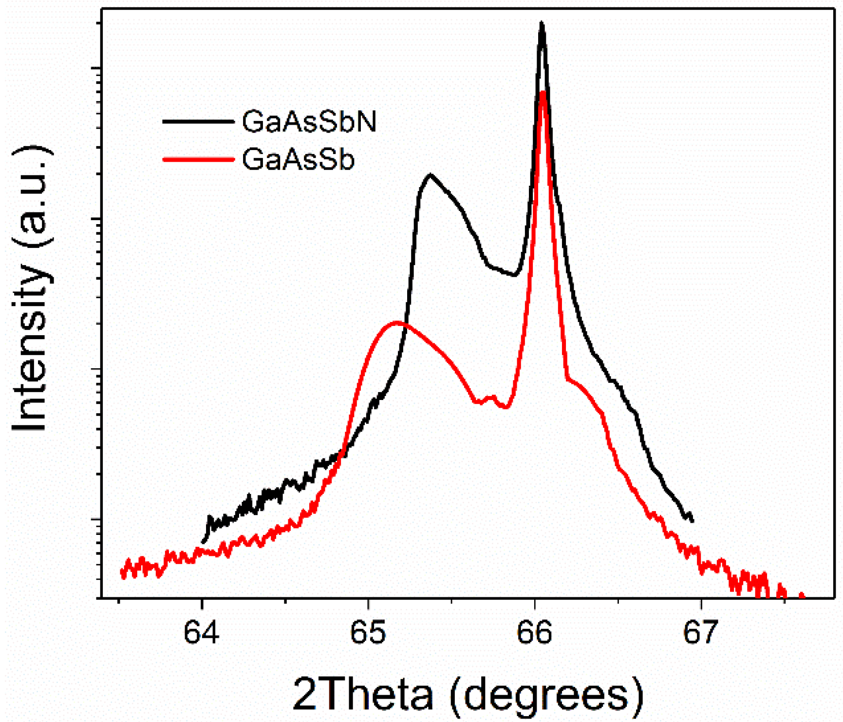
High-resolution XRD (004) scan spectra of GaAsSbN/GaAs and GaAsSb/GaAs samples are plotted in Figure 1. Two prominent peaks are seen in each spectrum. The sharp peaks with high intensity are associated with the GaAs substrate, while the weak broad peaks originate from the relaxed metamorphic GaAsSbN and GaAsSb layers. The thickness of the epitaxial layers measured by SEM is about 0.5–0.6 μm, i.e., above the critical thickness value of 250 nm, determined theoretically and experimentally in refs. [28,29], respectively. The lattice mismatch ∆a/a0, estimated from the distance between the XRD peaks, is about 0.48% for GaAsSbN [14] and 0.63% for GaAsSb [23]. The smaller mismatch of GaAsSbN is explained by the effect of nitrogen, which partially compensates for the lattice extension by the large Sb atoms. Using the Sb content of 6.8%, found separately by EDX, and applying Vegard’s law for the lattice constant of relaxed layers, we estimate the N content in the crystal lattice of GaAsSbN to be ~0.1% [14]. The Sb content in GaAsSb determined from the XRD spectrum is 8%, which is in agreement with the EDX and XPS results [23].
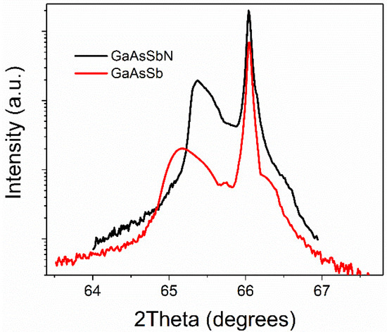
Figure 1.
High-resolution X-ray diffraction (004) curves of GaAsSbN and GaAsSb layers.
3.2. AFM Measurements
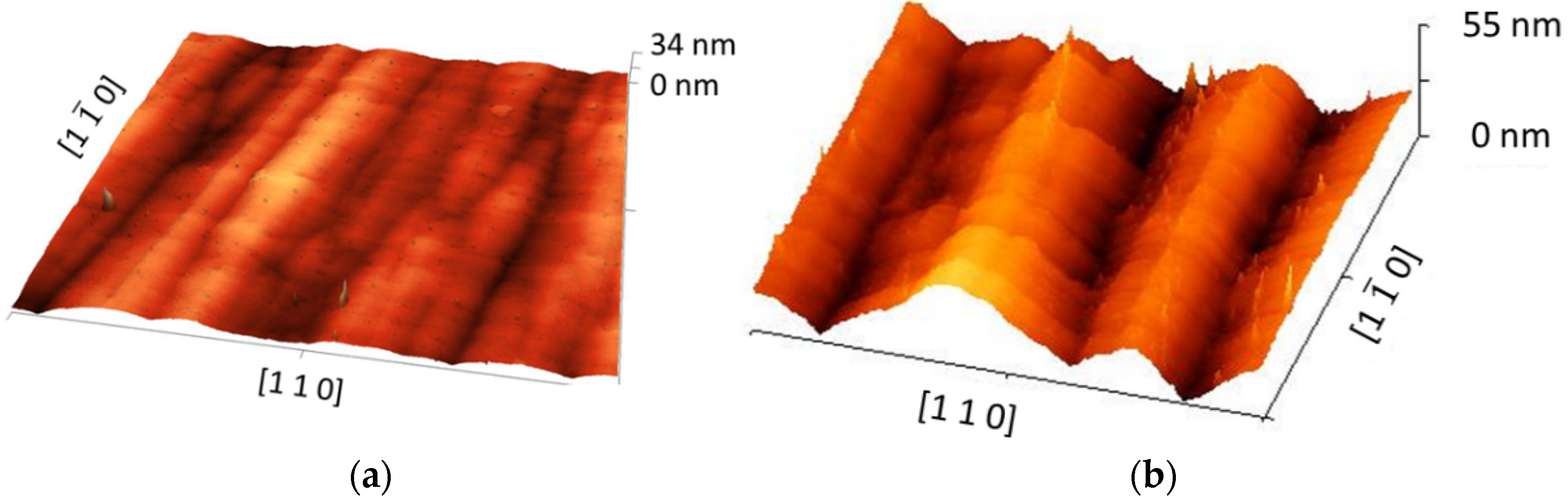
AFM is a simple method to identify the dominant type of defects from the surface morphology. Figure 2a,b show the 3D AFM images of a 20 × 20 μm2 area of the as-grown GaAsSbN and GaAsSb layer surfaces. They reveal a cross-hatch structure with strong anisotropy in the two orthogonal <110> directions. Well-defined ridges oriented along the directions are clearly seen, while those along the orthogonal directions are less visible. This relief depends on the plastic relaxation of the metamorphic layer and the generation of misfit dislocations at the layer/substrate interface [30,31,32]. Such a type of anisotropic relaxation inhibits the creation of threading dislocations in the grown layers [33,34]. Some breaking of a few ridges is seen in the AFM image of GaAsSbN, which could be explained by N-related defects, in addition to misfit dislocations at the interface. The RMS roughness values of the two samples are 7.5 nm for GaAsSb and 3.3 nm for GaAsSbN. The higher roughness of GaAsSb is due to the higher lattice mismatch between the GaAs substrate and the epitaxial GaAsSb layer.

Figure 2.
AFM surface topography image of (a) GaAsSbN and (b) GaAsSb layers.
4. Characterization of the Photoresponse
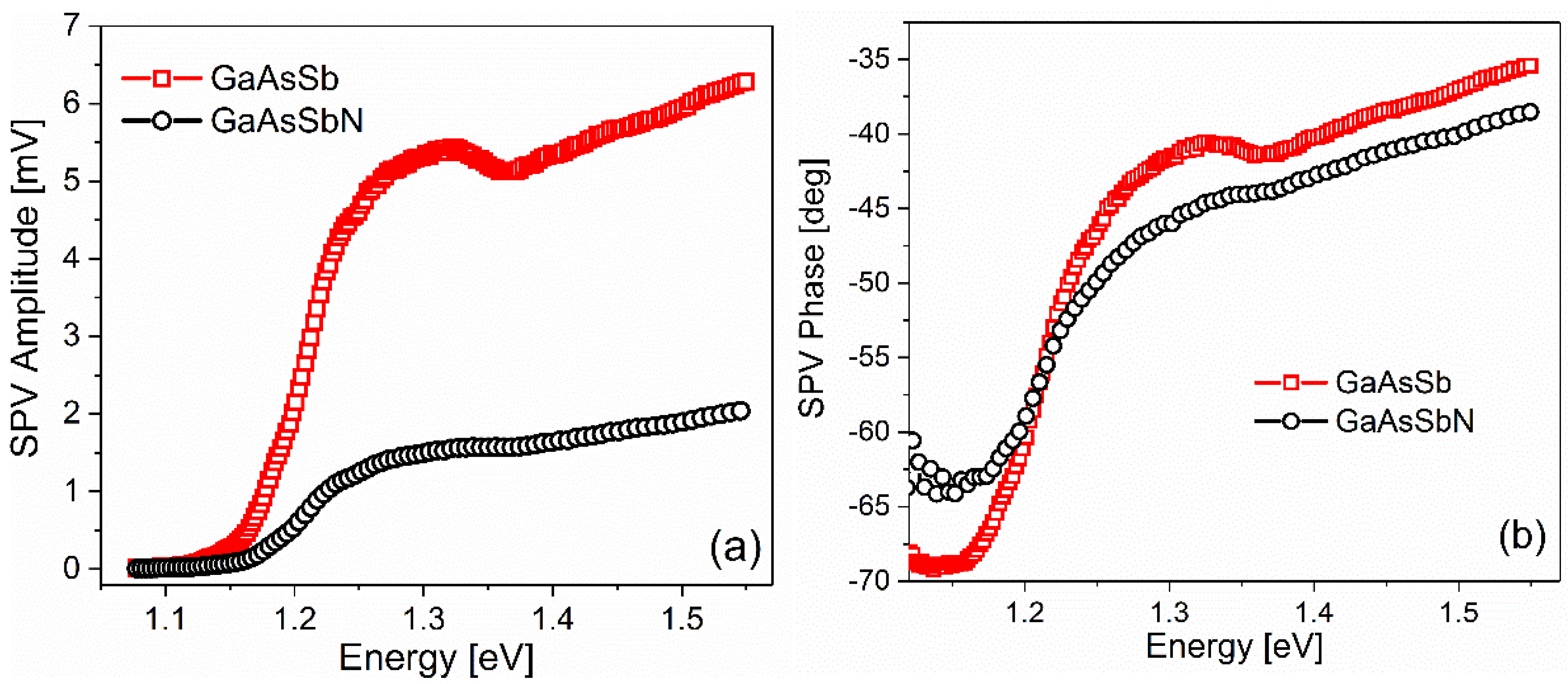
The SPV amplitude spectrum is known to emulate the optical absorption spectrum, while the SPV phase indicates the direction of the photocarrier transport in the sample [26,27]. Figure 3 presents the SPV amplitude and phase spectra of GaAsSbN and GaAsSb layers grown on GaAs substrates using the same temperature regime. Both amplitude spectra reveal a step at low energies, which finishes as a broad peak at around 1.32 eV. This spectral structure results from band-to-band optical transitions in the epitaxial layer of GaAsSbN or GaAsSb. The SPV phase in this range is in the IVth quadrant (Figure 3b), indicating an upward energy band bending in the epitaxial layers in the direction toward the surface and n-type residual doping [27]. Therefore, the photogenerated electrons in the layers move toward the substrate, while the holes move towards the surface. The bandgap energy of the layers was determined by Tauc plots, as shown in Figure 4 for GaAsSb. Similar values are found for the two layers, namely, 1.193 eV for GaAsSbN and 1.194 eV for GaAsSb.
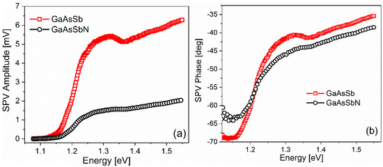
Figure 3.
Surface photovoltage amplitude (a) and phase (b) spectra of GaAsSbN/GaAs (black circles) and GaAsSb/GaAs (red squares) structures.
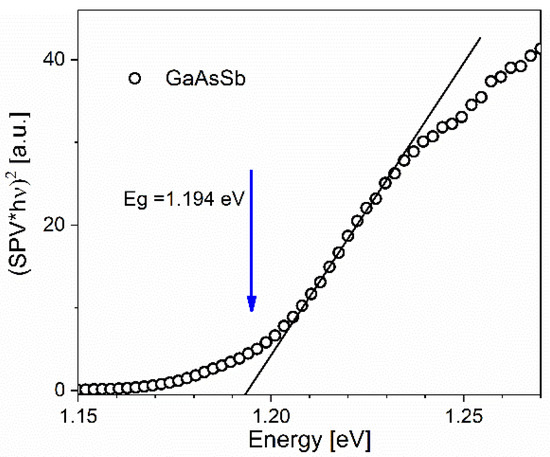
Figure 4.
Tauc plot of the SPV spectrum of GaAsSb.
At higher energies, the SPV amplitude continues increasing, which is due to the inclusion of optical absorption in the GaAs substrate. Indeed, keeping in mind the thickness of the epitaxial layers and a typical value for the GaAsSb (N) optical absorption coefficient 2 × 104 cm−1 [35], part of the impinging photons reach the GaAs substrate and generate free carriers via band-to-band transitions. The SPV phase at these energies is also in the IVth quadrant, which shows that the bending of the energy bands at the interface layer/substrate is also upward. Such bending is expected because of the high n-type doping of the substrate.
The shape of the SPV phase spectrum is very similar to, and practically follows, the SPV amplitude spectrum for both types of structures. Bearing in mind that the photon flux density is kept constant during the scan, the increase in the photon energy is accompanied by increasing the optical absorption coefficient. The SPV phase changes anti-clockwise with increasing the photon energy. This means that the SPV phase delay, relative to the optical excitation, decreases with increasing the optical absorption coefficient [27]. Such behaviour of the SPV phase delay suggests a decrease in the effective carrier lifetime with increasing the generation rate of free carriers, i.e., a non-linear recombination regime in the GaAsSbN and GaAsSb layers [27]. We suppose that this is connected with the domination of carrier recombination via defect levels in the bandgap. As discussed in [36], in such conditions, the effective carrier lifetime depends on the free carrier generation rate, leading to non-linear recombination kinetics because the concentration of excess minority carriers (holes in this case) cannot be neglected relative to their equilibrium concentration, which is very low. Therefore, the observed SPV phase behaviour suggests a large concentration of defect levels in the bandgap, which act as effective recombination centres.
Although GaAsSbN and GaAsSb have similar values of the IR photosensitivity edge, the photoresponse signal from the GaAsSb/GaAs structure is more than three times higher than the signal from the GaAsSbN/GaAs structure. This is more pronounced for photon energies corresponding to the absorption in the epitaxial layer, as can be seen from the normalized spectra, presented in Figure 5. The weaker SPV signal from the GaAsSbN/GaAs structure could be explained by a higher concentration of recombination centres in the GaAsSbN layers that deteriorate the optical and photovoltaic quality of the material. Nitrogen atoms are incorporated primarily in the As sublattice, replacing As atoms, which is associated with the appearance of different N-related point defects. They affect the quality of the compound since they introduce bandgap levels, which increase carrier recombination in their transport process and decrease carrier collection efficiency. The most common among them are AsGa antisite, interstitial Ga, and split interstitial N–As complexes [37,38]. In addition, carrier-trapping centres, such as N–Si defect complexes, exist in the bulk layers [39]. Nitrogen-related recombination centres destroy the optical quality of the compounds more than defects arising from the interface in GaAsSb/GaAs with lower crystal quality. The lower SPV signal originating from the GaAs substrate in the case of GaAsSbN/GaAs compared to GaAsSb/GaAs could be explained by the diffusion of N atoms into the substrate during LPE growth. The small amount of nitrogen deteriorates the optoelectronic properties of the GaAs material [40,41]. Despite its lower crystalline quality, GaAsSb exhibits a significantly higher photoresponse, since it does not contain nitrogen-induced recombination centres.
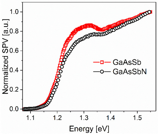
Figure 5.
Normalized SPV spectra of GaAsSbN/GaAs (black circles) and GaAsSb/GaAs (red squares) structures.
5. Conclusions
Two series of GaAsSbN and GaAsSb metamorphic layers were grown on GaAs substrates by low-temperature LPE. Characterization of their structural properties and photoresponse was carried out in a comparative plan. The GaAsSbN layers have better crystal quality because of the smaller lattice mismatch with the GaAs substrate, due to the compensation effect of N atoms in the As sublattice. The epitaxial layers of GaAs0.931Sb0.068N0.001 and GaAs0.92Sb0.08 exhibit similar IR photoresponse edges of ~1.2 eV. However, N-related point defects and complexes in GaAsSbN introduce recombination centres in the bandgap, which decreases the photoresponse compared to GaAsSb. The possibility to obtain a higher photoresponse from metamorphic GaAsSb layers makes this material an alternative to GaAsSbN for solar cell applications. The obtained results highlight the potential of the LPE method to grow GaAsSb layers with a high photoresponse. They can be the basis for further development of the technology to incorporate GaAsSb as a middle sub-cell into multi-junction solar cells based on III–V materials.
Author Contributions
Conceptualization, M.M.; methodology, M.M. and V.D.; validation, V.D. and M.M.; formal analysis, S.G. and V.D.; investigation, V.D. and S.G.; resources, M.M.; data curation, V.D.; writing—original draft preparation, M.M.; writing—review and editing, V.D.; visualization, S.G. and V.D.; supervision, V.D.; project administration, V.D.; funding acquisition, V.D. All authors have read and agreed to the published version of the manuscript.
Funding
This research was funded by the European Regional Development Fund, grant number BG05M2OP001-1.001-0008, and the Bulgarian Ministry of Education and Science, grant number D01-214/2018.
Institutional Review Board Statement
Not applicable.
Informed Consent Statement
Not applicable.
Data Availability Statement
Not applicable.
Acknowledgments
This work was supported by the European Regional Development Fund within the Operational Program “Science and Education for Smart Growth 2014–2020” under the Project CoE “National centre of mechatronics and clean technologies” BG05M2OP001-1.001-0008, and by the Bulgarian Ministry of Education and Science under the National Research Program E+: Low Carbon Energy for the Transport and Households, grant agreement D01-214/2018. Thanks are due to S. Russev and A. Zyapkov for the EDX and SEM measurements, to P. Terziyska and K. Krililov for the AFM measurements, and G. Avdeev for the XRD measurements.
Conflicts of Interest
The authors declare no conflict of interest.
References
- Wang, C.; Liu, M.; Rahman, S.; Pasanen, H.P.; Tian, J.; Li, J.; Deng, Z.; Zhang, H.; Vivo, P. Hydrogen Bonding Drives the Self-Assembling of Carbazole-Based Hole-Transport Material for Enhanced Efficiency and Stability of Perovskite Solar Cells. Nano Energy 2022, 101, 107604. [Google Scholar] [CrossRef]
- Li, R.; Li, C.; Liu, M.; Vivo, P.; Zheng, M.; Dai, Z.; Zhan, J.; He, B.; Li, H.; Yang, W.; et al. Hydrogen-Bonded Dopant-Free Hole Transport Material Enables Efficient and Stable Inverted Perovskite Solar Cells. CCS Chem. 2021, 3, 3309–3319. [Google Scholar] [CrossRef]
- Ahmad, J.; Bazaka, K.; Anderson, L.J.; White, R.D.; Jacob, M.V. Materials and Methods for Encapsulation of OPV: A Review. Renew. Sustain. Energy Rev. 2013, 27, 104–117. [Google Scholar] [CrossRef]
- Geisz, J.F.; Steiner, M.A.; Jain, N.; Schulte, K.L.; France, R.M.; McMahon, W.E.; Perl, E.E.; Friedman, D.J. Building a Six-Junction Inverted Metamorphic Concentrator Solar Cell. IEEE J. Photovolt. 2018, 8, 626–632. [Google Scholar] [CrossRef]
- Isoaho, R.; Aho, A.; Tukiainen, A.; Aho, T.; Raappana, M.; Salminen, T.; Reuna, J.; Guina, M. Photovoltaic Properties of Low-Bandgap (0.7–0.9 EV) Lattice-Matched GaInNAsSb Solar Junctions Grown by Molecular Beam Epitaxy on GaAs. Sol. Energy Mater. Sol. Cells 2019, 195, 198–203. [Google Scholar] [CrossRef]
- Miyashita, N.; Ahsan, N.; Okada, Y. Effect of Antimony on Uniform Incorporation of Nitrogen Atoms in GaInNAs Films for Solar Cell Application. Sol. Energy Mater. Sol. Cells 2013, 111, 127–132. [Google Scholar] [CrossRef]
- Aho, A.; Korpijärvi, V.M.; Isoaho, R.; Malinen, P.; Tukiainen, A.; Honkanen, M.; Guina, M. Determination of Composition and Energy Gaps of GaInNAsSb Layers Grown by MBE. J. Cryst. Growth 2016, 438, 49–54. [Google Scholar] [CrossRef]
- Kurtz, S.R.; Klem, J.F.; Allerman, A.A.; Sieg, R.M.; Seager, C.H.; Jones, E.D. Minority Carrier Diffusion and Defects in InGaAsN Grown by Molecular Beam Epitaxy. Appl. Phys. Lett. 2002, 80, 1379–1381. [Google Scholar] [CrossRef]
- Johnston, S.W.; Kurtz, S.R.; Friedman, D.J.; Ptak, A.J.; Ahrenkiel, R.K.; Crandall, R.S. Observed Trapping of Minority-Carrier Electrons in p-Type GaAsN during Deep-Level Transient Spectroscopy Measurement. Appl. Phys. Lett. 2005, 86, 072109. [Google Scholar] [CrossRef]
- Dawidowski, W.; Ściana, B.; Bielak, K.; Mikolášek, M.; Drobný, J.; Serafińczuk, J.; Lombardero, I.; Radziewicz, D.; Kijaszek, W.; Kósa, A.; et al. Analysis of Current Transport Mechanism in AP-MOVPE Grown GaAsN p-i-n Solar Cell. Energies 2021, 14, 4651. [Google Scholar] [CrossRef]
- Kim, T.W.; Forghani, K.; Mawst, L.J.; Kuech, T.F.; Lalumondiere, S.D.; Sin, Y.; Lotshaw, W.T.; Moss, S.C. Properties of “bulk” GaAsSbN/GaAs for Multi-Junction Solar Cell Application: Reduction of Carbon Background Concentration. J. Cryst. Growth 2014, 393, 70–74. [Google Scholar] [CrossRef]
- Gonzalo, A.; Stanojević, L.; Fuertes Marrón, D.; Guzman, A.; Hierro, A.; Ulloa, J.M. 1 EV GaAsSbN–Based Solar Cells for Efficient Multi-Junction Design: Enhanced Solar Cell Performance upon Annealing. Sol. Energy 2021, 221, 307–313. [Google Scholar] [CrossRef]
- Braza, V.; Reyes, D.F.; Gonzalo, A.; Utrilla, A.D.; Ulloa, J.M.; Flores, S.; Ben, T.; González, D. Compositional Inhomogeneities in Type-I and Type-II Superlattices for GaAsSbN-Based Solar Cells: Effect of Thermal Annealing. Appl. Surf. Sci. 2018, 459, 1–8. [Google Scholar] [CrossRef]
- Milanova, M.; Donchev, V.; Kostov, K.L.; Alonso-Álvarez, D.; Terziyska, P.; Avdeev, G.; Valcheva, E.; Kirilov, K.; Georgiev, S. Study of GaAsSb:N Bulk Layers Grown by Liquid Phase Epitaxy for Solar Cells Applications. Mater. Res. Express 2019, 6, 075521. [Google Scholar] [CrossRef]
- Aho, A.; Tukiainen, A.; Polojärvi, V.; Guina, M. Performance Assessment of Multijunction Solar Cells Incorporating GaInNAsSb. Nanoscale Res. Lett. 2014, 9, 61. [Google Scholar] [CrossRef]
- Yu, P.; Wu, J.; Gao, L.; Liu, H.; Wang, Z. InGaAs and GaAs Quantum Dot Solar Cells Grown by Droplet Epitaxy. Sol. Energy Mater. Sol. Cells 2017, 161, 377–381. [Google Scholar] [CrossRef]
- Baoxue, B.; Xin, G.; Wang, L.; Li, H.; Qu, Y. Rhombus-like Stripe BA InGaAs-AlGaAs-GaAs Lasers. IEEE Photonics Technol. Lett. 2004, 16, 1248–1249. [Google Scholar] [CrossRef]
- Ebert, C.W.; Reynolds, C.L.; Wellenius, P.; Reynolds, J.G.; Muth, J.F.; Pulwin, Z.; Lee, D.; Lu, F.; Dyer, D. Optimization of InGaAs Metamorphic Buffers for Triple Junction Solar Cells. In Proceedings of the Conference Record of the 37th IEEE Photovoltaic Specialists Conference, Seattle, WA, USA, 19–24 June 2011; pp. 469–473. [Google Scholar]
- Mathews, I.; O’Mahony, D.; Gocalinska, A.; Manganaro, M.; Pelucchi, E.; Schmidt, M.; Morrison, A.P.; Corbett, B. InAlAs Solar Cell on a GaAs Substrate Employing a Graded InxGa1−xAs–InP Metamorphic Buffer Layer. Appl. Phys. Lett. 2013, 102, 033906. [Google Scholar] [CrossRef]
- Gao, X.; Wei, Z.; Zhao, F.; Yang, Y.; Chen, R.; Fang, X.; Tang, J.; Fang, D.; Wang, D.; Li, R.; et al. Investigation of Localized States in GaAsSb Epilayers Grown by Molecular Beam Epitaxy. Sci. Rep. 2016, 6, 29112. [Google Scholar] [CrossRef]
- Suhandi, A.; Tayubi, Y.R.; Arifin, P. Growth of GaAsSb Thin Film by Vertical MOCVD and Their Characterization. J. Eng. Appl. Sci. 2016, 11, 2788–2793. [Google Scholar]
- Sharma, A.S.; Das, S.; Dhar, S. Control of the Composition and the Structural Properties of GaAsSb Layers, Grown by Liquid Phase Epitaxy, by Bi Addition to the Growth Melt. J. Cryst. Growth 2020, 545, 125739. [Google Scholar] [CrossRef]
- Donchev, V.; Milanova, M.; Kirilov, K.; Georgiev, S.; Kostov, K.L.; Piana, G.M.; Avdeev, G. Low-Temperature LPE Growth and Characterization of GaAsSb Layers for Photovoltaic Applications. J. Cryst. Growth 2021, 574, 126335. [Google Scholar] [CrossRef]
- Gratton, M.F.; Woolley, J.C. Investigation of Two- and Three-Phase Fields in the Ga-As-Sb System. J. Electrochem. Soc. 1980, 127, 55. [Google Scholar] [CrossRef]
- Mani, H.; Joullie, A.; Karouta, F.; Schiller, C. Low-temperature Phase Diagram of the Ga-As-Sb System and Liquid-phase-epitaxial Growth of Lattice-matched GaAsSb on (100) InAs Substrates. J. Appl. Phys. 1986, 59, 2728–2734. [Google Scholar] [CrossRef]
- Kronik, L.; Shapira, Y. Surface Photovoltage Phenomena: Theory, Experiment, and Applications. Surf. Sci. Rep. 1999, 37, 1–206. [Google Scholar] [CrossRef]
- Donchev, V. Surface Photovoltage Spectroscopy of Semiconductor Materials for Optoelectronic Applications. Mater. Res. Express 2019, 6, 103001. [Google Scholar] [CrossRef]
- Dodson, B.W.; Tsao, J.Y. Relaxation of Strained-Layer Semiconductor Structures via Plastic Flow. Appl. Phys. Lett. 1987, 51, 1325–1327. [Google Scholar] [CrossRef]
- Maros, A.; Faleev, N.; King, R.R.; Honsberg, C.B.; Convey, D.; Xie, H.; Ponce, F.A. Critical Thickness Investigation of MBE-Grown GaInAs/GaAs and GaAsSb/GaAs Heterostructures. J. Vac. Sci. Technol. B Nanotechnol. Microelectron. Mater. Process. Meas. Phenom. 2016, 34, 02L113. [Google Scholar] [CrossRef]
- Andrews, A.M.; Speck, J.S.; Romanov, A.E.; Bobeth, M.; Pompe, W. Modeling Cross-Hatch Surface Morphology in Growing Mismatched Layers. J. Appl. Phys. 2002, 91, 1933–1943. [Google Scholar] [CrossRef]
- Hudait, M.K.; Lin, Y.; Palmisiano, M.N.; Tivarus, C.; Pelz, J.P.; Ringel, S.A. Comparison of Mixed Anion, InAsyP1-y and Mixed Cation, InxAl1-xAs Metamorphic Buffers Grown by Molecular Beam Epitaxy on (100) InP Substrates. J. Appl. Phys. 2004, 95, 3952–3960. [Google Scholar] [CrossRef]
- Saha, S.; Cassidy, D.T.; Thompson, D.A. Investigation of Cross-Hatch in In0.3Ga0.7As Pseudo-Substrates. J. Appl. Phys. 2013, 113, 124301. [Google Scholar] [CrossRef]
- Gangopadhyay, A.; Maros, A.; Faleev, N.; Smith, D.J. Strain Relaxation in Low-Mismatched GaAs/GaAs1-XSbx/GaAs Heterostructures. Acta Mater. 2019, 162, 103–115. [Google Scholar] [CrossRef]
- O’Reilly, A.J.; Quitoriano, N.J.; O’Reilly, A.J.; Quitoriano, N.J. Reduction of Threading Dislocation Density in SiGe Epilayer on Si (001) by Lateral Growth Liquid-Phase Epitaxy. J. Cryst. Growth 2018, 483, 223–227. [Google Scholar] [CrossRef]
- Kim, T.J.; Le, V.L.; Nguyen, H.T.; Nguyen, X.A.; Kim, B.; Kim, Y.D. Parameterization of the Dielectric Function of GaAsSb Alloy Films. J. Korean Phys. Soc. 2020, 77, 840–844. [Google Scholar] [CrossRef]
- Bonch-Bruevich, V.L.; Kalashnikov, S.G. Fizika Poluprovodnikov (Physics of Semiconductors); Nauka: Moscow, Russia, 1977. [Google Scholar]
- Laukkanen, P.; Punkkinen, M.P.J.; Puustinen, J.; Levämäki, H.; Tuominen, M.; Schulte, K.; Dahl, J.; Lång, J.; Zhang, H.L.; Kuzmin, M.; et al. Formation and Destabilization of Ga Interstitials in GaAsN: Experiment and Theory. Phys. Rev. B Condens. Matter Mater. Phys. 2012, 86, 195205. [Google Scholar] [CrossRef]
- Chen, W.M.; Buyanova, I.A.; Tu, C.W.; Yonezu, H. Point Defects in Dilute Nitride III-N-As and III-N-P. Phys. B Condens. Matter 2006, 376, 545–551. [Google Scholar] [CrossRef]
- Reason, M.; Jin, Y.; McKay, H.A.; Mangan, N.; Mao, D.; Goldman, R.S.; Bai, X.; Kurdak, C. Influence of N on the Electronic Properties of GaAsN Alloy Films and Heterostructures. J. Appl. Phys. 2007, 102, 103710. [Google Scholar] [CrossRef]
- Zhang, S.B.; Wei, S.-H. Theory of Defects in Dilute Nitrides. In Physics and Applications of Dilute Nitrides; Irina, A., Buyanova, W., Chen, M., Eds.; Taylor & Francis: Abingdon, UK, 2005; pp. 239–270. [Google Scholar]
- Krispin, P.; Gambin, V.; Harris, J.S.; Ploog, K.H. Nitrogen-Related Electron Traps in Ga(As,N) Layers (<<3%N). J. Appl. Phys. 2003, 93, 6095–6099. [Google Scholar] [CrossRef]


Publisher’s Note: MDPI stays neutral with regard to jurisdictional claims in published maps and institutional affiliations. |
© 2022 by the authors. Licensee MDPI, Basel, Switzerland. This article is an open access article distributed under the terms and conditions of the Creative Commons Attribution (CC BY) license (https://creativecommons.org/licenses/by/4.0/).