Article

Validation through Experiment and Simulation of Internal Charging–Discharging Characteristics of Polyimide under High-Energy Electron Radiation

1
School of Electronics and Information, Xi’an Polytechnic University, Xi’an 710048, China
2
Yangtze Delta Region Institute (Huzhou), University of Electronic Science and Technology of China, Huzhou 313001, China
3
State Key Laboratory of Electrical Insulation and Power Equipment, Xi’an Jiaotong University, Xi’an 710049, China
4
State Grid Yangzhou Power Supply Company, Yangzhou 225100, China
*
Author to whom correspondence should be addressed.
Energies 2022, 15(18), 6603; https://doi.org/10.3390/en15186603
Submission received: 4 August 2022 / Revised: 26 August 2022 / Accepted: 6 September 2022 / Published: 9 September 2022

Abstract

:
Due to the injection of energetic particles, such as electrons in space environment, the internal charging–discharging characteristics of spacecraft dielectrics need to be evaluated for the safety of spacecraft, and the evaluation results from experiments and simulations should be comparatively validated. An in-site pulsed electroacoustic (PEA) measurement system under high-energy electron radiation was established for evaluating the charging characteristics of thick plate samples about 3 mm, while a joint simulation method based on Geant4 and COMSOL was also proposed. The deposited charge distributions were compared through experiment and joint simulation method under 0.7, 1.0 and 1.3 MeV for 30 min and 1.0 MeV for 10, 60 and 120 min, respectively. Meanwhile, the electrostatic discharging characteristics were also comparative evaluated by both methods under 0.3 MeV for 20 min under 5, 10 and 15 µA beam current, and the total discharging times and initial discharging time were compared and analyzed. Overall, a good consistency existed between experimental and simulation results of charging–discharging characteristics under electron radiation while the difference was also analyzed in the perspective of dielectric properties, such as charge leakage by conduction. Through the comparative study, both evaluation methods are validated, which offers effective reference for the safety evaluation of spacecraft dielectrics in future.

1. Introduction

The space environment is one of the most complex and changeable environments known so far. The interaction between energetic particles, such as high-energy electrons and the spacecraft dielectrics, can easily lead to the charging–discharging phenomena of the materials, which threatens the safe operation of the spacecraft [1,2]. When the high-energy electrons (0.1~10 MeV) penetrate the shielding layer and are eventually deposited inside the dielectric, the internal charging appears. Since the charge release rate of the dielectric material is much lower than its charge deposition rate, the accumulation of charges inside can easily lead to electric field concentration. When the electric field strength generated by the deposited charges exceeds the breakdown threshold of the material, electrostatic discharge (ESD) will be induced [3,4]. Therefore, to ensure the operational safety and long life of the spacecraft, the internal charging level of the dielectrics should be evaluated in a space radiation environment.
At present, there are mainly three types of charging–discharging evaluation methods: flight experiment, ground simulated experiment and calculation method. However, due to the high expense of in-orbit experiment, most institutions and researchers focus on the latter two. In ground simulated experiments, the pulsed electroacoustic (PEA) method is widely used for deposited charge measurement of insulating materials [5,6,7], while the in-situ measurement technology of deposited charges under electron radiation are also proposed [8]. The French Laurent team improved the classic PEA into “short-circuit PEA” and “open-circuit PEA”, which was suitable for the measurement under electron radiation [9]. Griseri designed an in-situ PEA measurement system of flat specimens under electron radiation and measured Teflon and Kapton less than 500 µm [10]. Perrin also proposed an improved open-circuit PEA method for measuring the space charge distribution after the electron radiation [11]. Arnaout designed a non-contact in-situ measurement device of space charge to analyze charge transportation in materials under high-energy electron radiation [12]. However, the recent reported in-situ measurement technology under high-energy electron radiation is only suitable for plate sample at micrometer level, which cannot meet the requirement of millimeter-level samples in the spacecraft.
Another research hotspot for the charging–discharging phenomena of dielectrics is simulation method. The interaction between high-energy electrons and the dielectrics under space environment is simulated to obtain data, such as the charge deposition rate and dose rate, and then the internal electric field distribution is solved by charge transportation model [13]. Aerospace institutions and universities in various countries have developed evaluation codes, such as NUMIT (NUMerical InTegration), DICTAT (DERA Internal Charging Threat Assessment Tool), SPIS (Spacecraft Plasma Interaction System) and Geant4 (GEometry ANd Tracking) for internal charging of the dielectric by 1D and 3D models [14,15,16,17,18]. ESA used DICTAT to develop a 1D computational evaluation method for the internal charging of dielectrics [14]. Kim developed a 3D NUMIT evaluation software suitable for dielectric and suspended conductor structures based on the Monte Carlo method [19]. Zuo obtained deposition electric parameters by the Monte Carlo simulation and numerically solved the distributions of the electric field and potential in the dielectric material [20]. Combined with finite element software, Tang simulated the interaction process of high-energy electrons and dielectrics based on Geant4, and the internal electric field distribution of the 3D circuit board model was constructed and analyzed under high-energy electron radiation [21]. Li established a 2D simulation model to obtain the electric field distribution in the complex structure of solar array driving assembly (SADA) [22]. To optimize the radiation resistance of the SADA structure, Wang also used ground simulated experiments and 3D numerical simulation [23]. Based on the bipolar charge transport process, Wang established a deep dielectric charging model of a SADA under the coupling effect of electron irradiation and operating voltage [24]. These developed methods for evaluating the internal charging characteristics in 3D dielectrics are basically based on the Monte Carlo method, which is a proven and feasible method.
In the field of internal charging–discharging evaluation of spacecraft dielectrics, deficiencies still exist in the experimental evaluation method. Although the simulation methods provide supplement, there are often certain differences among different methods. Therefore, the evaluation effectiveness of internal charging encounters certain challenges. Focusing on this technical bottleneck, we evaluate the internal charging–discharging characteristics for spacecraft dielectric polyimide (PI) under high-energy electron radiation by the experimental and simulation methods, respectively. In the charging process, by an in-situ PEA method under high-energy electron radiation, the charge distribution of PI was tested and compared with data from a joint simulation method of Geant4 and COMSOL. In the evaluation of the discharging, the experimental method and the joint simulation method were also used and compared for the total discharging times and initial discharging time under three groups of beam currents.

2. Experiment and Simulation Methods of Internal Charging–Discharging under High-Energy Electron Radiation

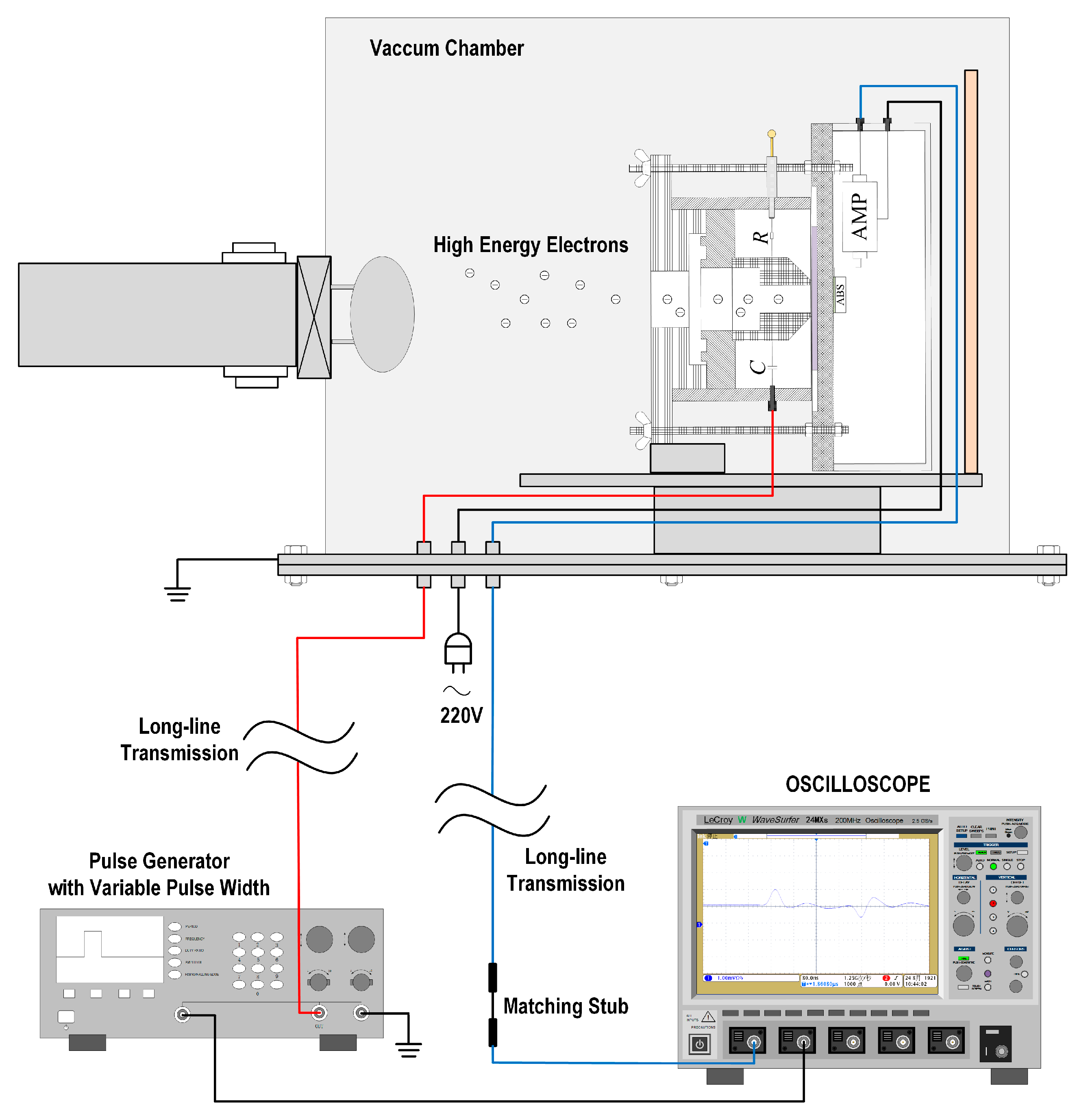
2.1. Measurement System of Charge Distribution under High-Energy Electron

2.1.1. Design of Electrode System

Compared with the traditional space charge distribution measurement system by PEA, the electrode system was redesigned, as shown in Figure 1. This system had two measurement modes, namely the space charge distribution under high-energy electron radiation and traditional DC high voltage, and the former was mainly used here. To realize the radiation of high-energy electrons to the sample, a hollow metal collimator was added to the upper electrode, so the high-energy electrons could pass through and be injected into the dielectric. The pulse signal with variable width was drawn from a pulse source and applied to the sample through a 0.5 mm aluminum sheet. The rising and falling edge of the pulse were both 7 ns with a half-peak width of 90 ns, and the amplitude ranged from 0 to 3600 V with a coupling capacitance of 4700 pF. In the lower electrode, a PVDF sensor with a thickness of 100 μm was used, together with an amplifier-type HAS-X-1-40 AC by FEMTO. The amplified voltage signal was then sent to the oscilloscope.
To further carry out in-situ measurement under high-energy electron radiation, the whole electrode system was placed in the vacuum chamber, as shown in Figure 2, and the pulse and the measurement signals were transmitted through a long-distance transmission line. So, a short matching wire was connected to eliminate distortion of the measurement signal after long-distance transmission. For the in-site measurement, the deposited charge inside the sample originated from high-energy electrons, thus only a pulse was needed to measure the charge distribution.

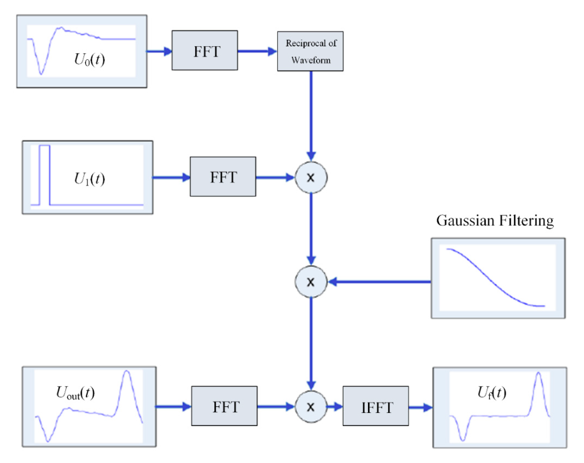
2.1.2. Waveform Recovery of Space Charge Distribution

The observed voltage signal of the PEA measurement is distorted by the reflection of acoustic waves at the interface between the piezoelectric sensor and the absorbing material, which is known as a systematic error. So, it is necessary to perform waveform recovery processing and obtain the real space charge distribution. The principle is as follows [25,26,27]. The obtained voltage signal Uout(t) can be represented by the convolution of the excitation response h(t) of the system and the charge distribution Uf(t) as follows:
U o u t ( t ) = h ( t ) U f ( t ) = + h ( t τ ) U f ( τ ) d τ
By obtaining the excitation response h(t), the charge distribution could be calculated by deconvolution techniques. Equation (1) can be simply described in the frequency domain.
U o u t ( f ) = U f ( f ) H ( f )
where Uout(f), Uf(f) and H(f) are the Fourier transforms of Uout(t), Uf(t) and h(t) in the frequency domain, respectively, while H(f) is called the transfer function of the system. To obtain the transfer function of the system, the impulse response of the system must be obtained. Therefore, a reference signal U0(t) was generally selected from a sample with few internal defects, and the measured waveform was ensured without obvious charge injection under DC voltage application mode. Therefore, the specific process of waveform recovery is shown in Figure 3.
In Figure 3, U0(t) was the reference signal and U1(t) was a standard pulse equal to the peak value of U0(t). Uout(t) was the output voltage observed by the oscilloscope, and Uf(t) was the real space charge signal after processing. The reciprocal of the U0(f) multiplying by U1(f) gave the reciprocal of the transfer function H−1(f). After Gaussian filtering, H−1(f) was multiplied by U0(t) to obtain the Uf (f), and then the recovered signal Uf(t) can be obtained by inverse Fourier transform.

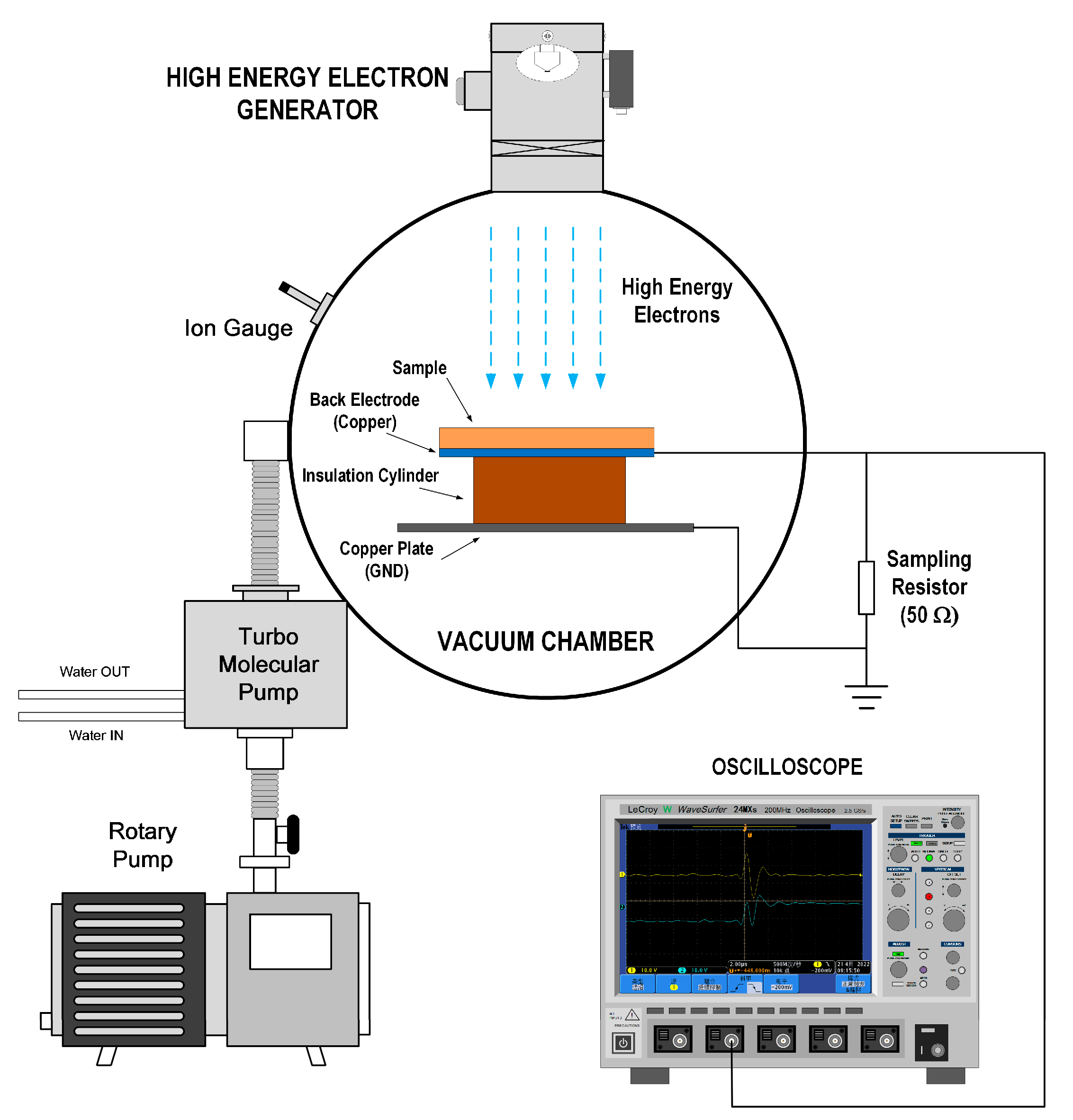
2.2. Measurement System of Electrostatic Discharging under High-Energy Electron Radiation

The internal electrostatic discharging (ESD) testing system under high-energy electron radiation mainly included a high-energy electron generator (CGN Dasheng Accelerator Technology Co., Ltd., Suzhou, China), a vacuum system and a signal measurement system. The electron beam current was adjustable from 0.2 to 100 μA, the electron energy ranged from 0.3 MeV to 0.5 MeV. The sample was placed in a vacuum chamber with a vacuum degree lower than 5 × 10⁻⁴ Pa. Due to the unstable beam current at the initial moment, a movable metal shield plate was set above the sample until the high-energy electron accelerator was stabilized for 20 min. Then, the beam current was adjusted to the specified value and the shield plate was removed. To monitor the discharging signal, the back of the sample was covered by a copper tape and grounded through a 50 Ω resistor. A column-shaped insulator was used to isolate the sample from the grounded working plate. All connecting wires were cables with grounded shielding layer. The ESD signal, including the voltage waveform and the discharging times, was recorded. The schematic diagram of the test system is shown in Figure 4.

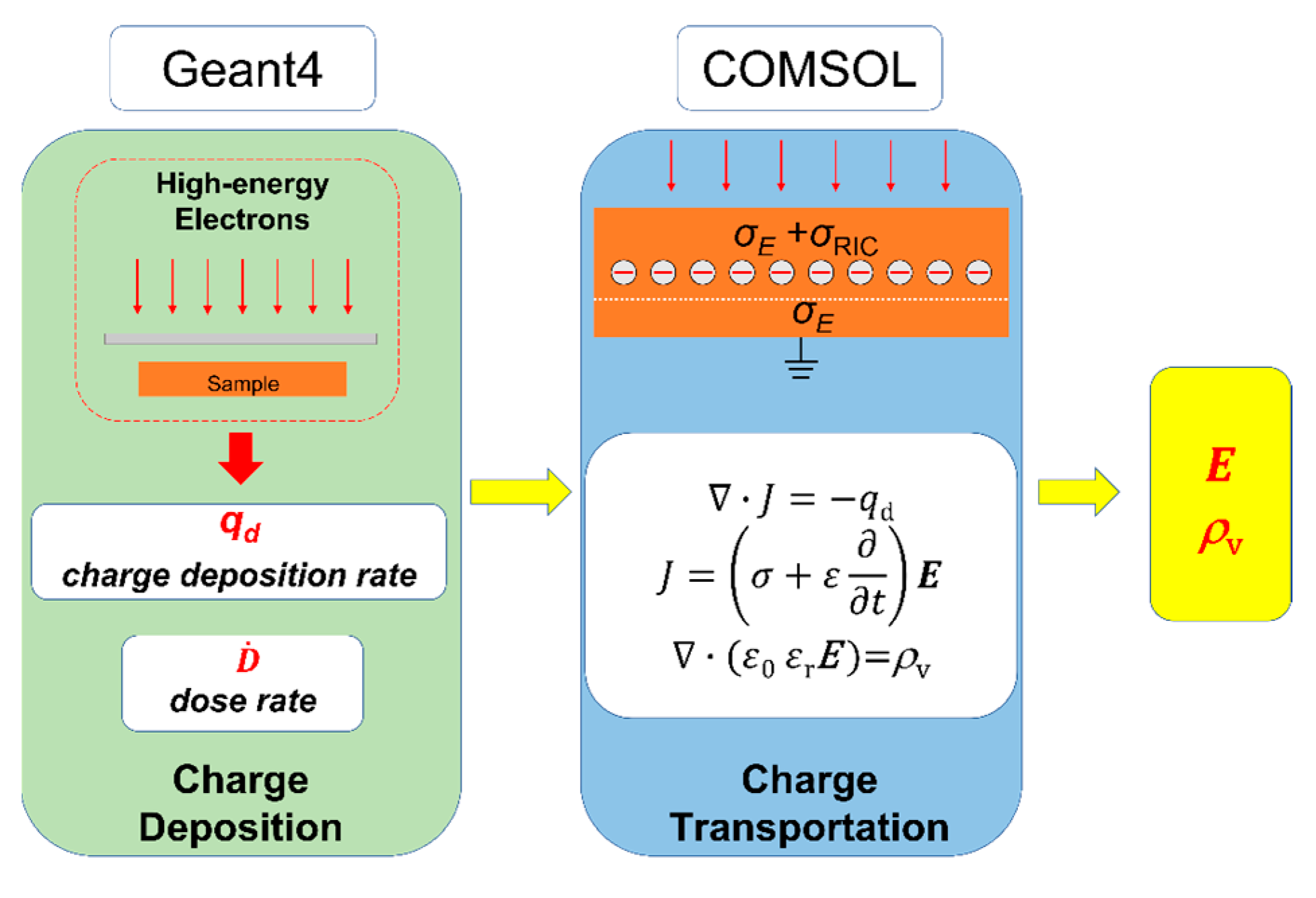
2.3. Joint Simulation Method of Internal Charging Characteristics under High-Energy Electron Radiation

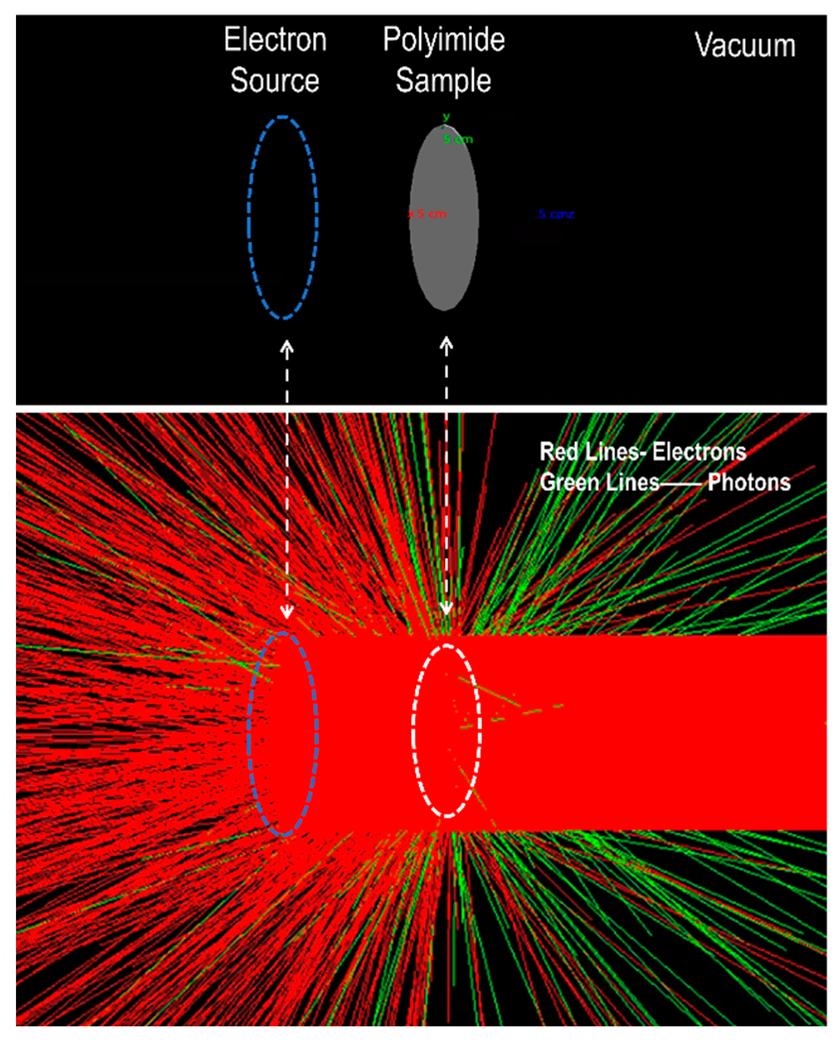
2.3.1. Electron Injection Process

Before the calculation of the electron deposition under high-energy electron radiation in Geant4, the basic model was firstly established according to the parameters of sample used in experiment. Then, the model was divided into several square meshes, and the charge deposition rate and radiation dose rate were counted based on Equations (3)–(5).
t = N i e j i S
q d = j i S q N i V
D = Δ D t
where t is the “virtual time” of radiation; Ni is the number of simulated electrons; ji is the electron flux; S is the radiation source area, m2; V is the mesh volume; q is the charge deposition rate per unit volume; qd is the charge deposition rate; ΔD is the radiation dose; D is the radiation dose rate. After calculation, the charge deposition rate and radiation dose rate were imported into COMSOL software in the form of interpolation function [28].

2.3.2. The 3D Charge Transportation Model

The charge conservation law (CCL) model was used as the charge transportation model [29], and the calculation equations are given by (6)–(8).
J = q d
J = ( σ + ε 0 ε r t ) E
E = ρ V ε 0 ε r
where J is the current density, which is the sum of the conduction current density and displacement current density, A; σ is the bulk conductivity, S/m; ε is the permittivity; E is the electric field strength, V/m. Based on the CCL solution method, the calculation of electric field strength and charge distribution could be performed in COMSOL.

2.3.3. Joint Simulation Method under High-Energy Electron Radiation

The joint simulation method of the Geant4 and COMSOL could acquire the charge deposition distribution and the internal electric field strength of the dielectric under high-energy electron radiation. The joint simulation method is shown in Figure 5.
Under the electron radiation, the bulk conductivity, σ, might be affected by many factors. Here, we mainly considered two points in the calculation: one was the appearance of radiation-induced conduction, and the other was the variation of bulk conductivity caused by enhanced electric field. When the high-energy electrons collide with the material, the electrons will transfer energy to the target atoms in the material, which leads to the excitation or ionization process, and thus the sharp increase in conductivity [30]. The increased part is called radiation-induced conductivity, σRIC, which is represented by Equations (9)–(11).
σ RIC = k RIC ( T ) D Δ ( T )
Δ ( T ) = [ 1 + T / T RIC ] 1
k RIC ( T ) = k RIC 0 k RIC 1 Δ ( T ) [ T / T RIC ] 3 / 2 2 Δ ( T )
where Δ(T) is the coefficient generally ranges 0.5–1.0; kRIC(T) is the radiation-induced conductivity coefficient, S·m−1·rad−1·s; kRIC0 is proportional to carrier mobility; kRIC1 is related to temperature and depends on the probability of carriers in the conduction band.
On the other hand, the electric field has a large influence on conductivity of dielectrics, which is called the electric-field-related conductivity, σE. In general, the Poole–Frenkel effect is used to calculate the σE but some studies show that neither Schottky effect nor Poole–Frenkel effect in PI can completely explain the charge transport process. Based on our previous experimental research, we employed the piecewise conductance calculation method to determine σE, as shown in Equation (12).
σ E = 3.6 × 10 17   S / m     0 < E < 10 7 ( V / m ) 3 × 10 15 6.1 × 10 9 E   S / m   10 7 < E < 4.9 × 10 7   ( V / m ) 1.9 × 10 13 9.1 × 10 6 E S / m E > 4.9 × 10 7 ( V / m )  

3. Evaluation Results of Internal Charging under High-Energy Electron Radiation

3.1. Internal Charging at Different Electron Energies

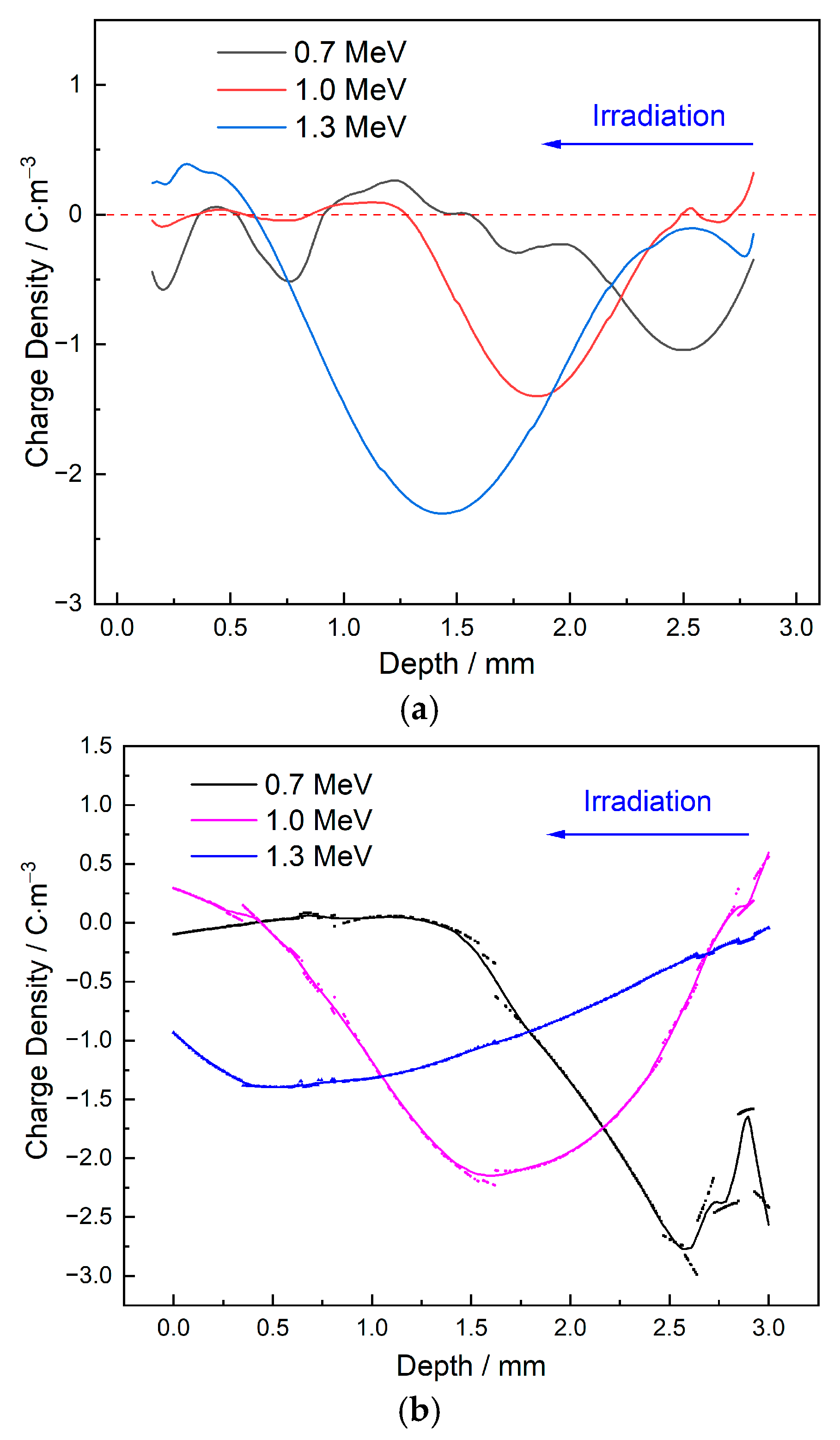
3.1.1. Space Charge Distribution Based on In-Situ PEA Method

A 3 mm thick PI plate sample was chosen for in-situ measurement experiments. The samples were irradiated for 30 min at 200 pA/cm2 beam density with energies of 0.7 MeV, 1.0 MeV and 1.3 MeV, respectively. Figure 6 shows the original voltage waveform under 1.3 MeV electron radiation. The voltage waveform under different electron energies was further processed by the space charge waveform recovery program, so as to obtain the deposition charge distribution.

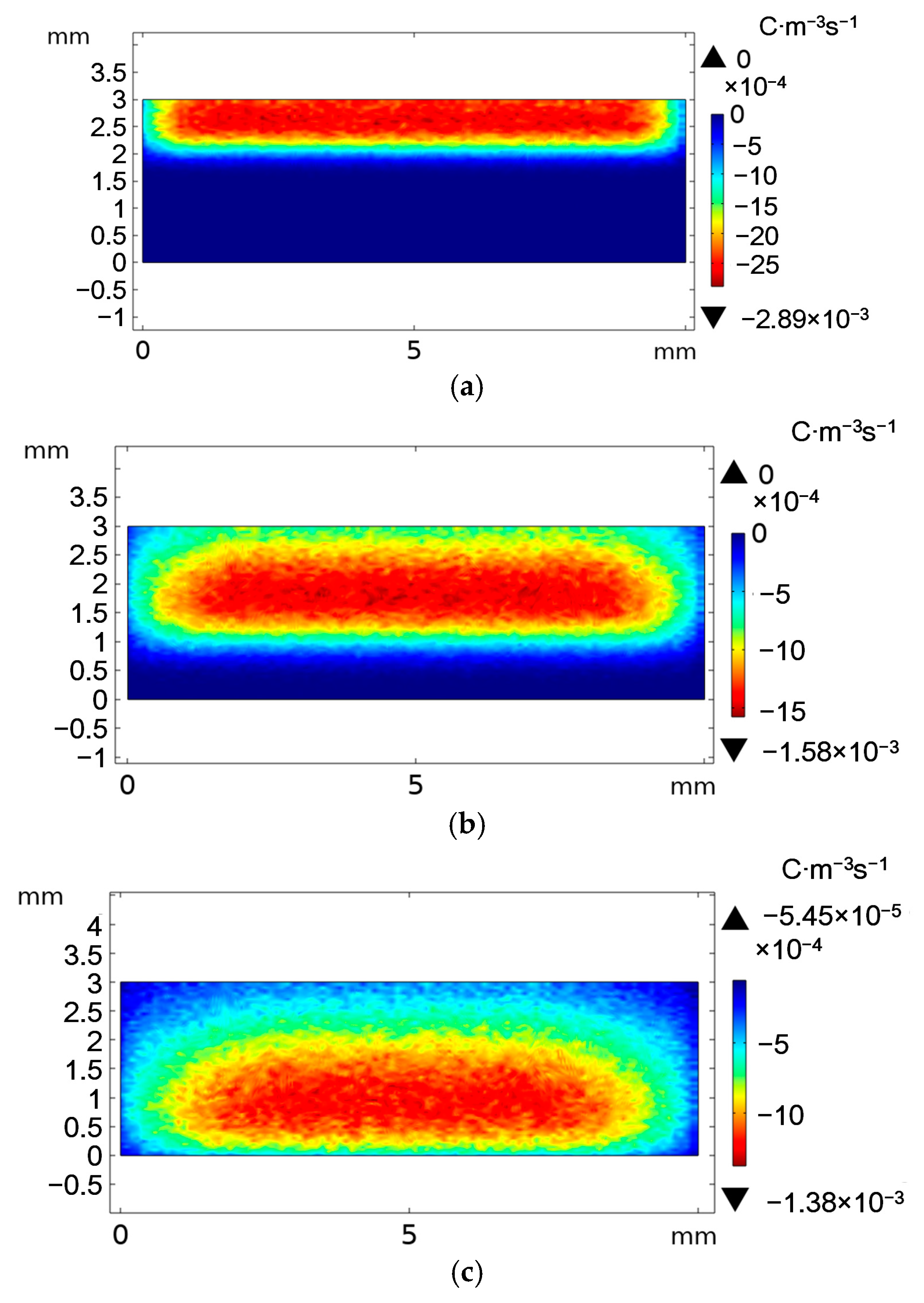
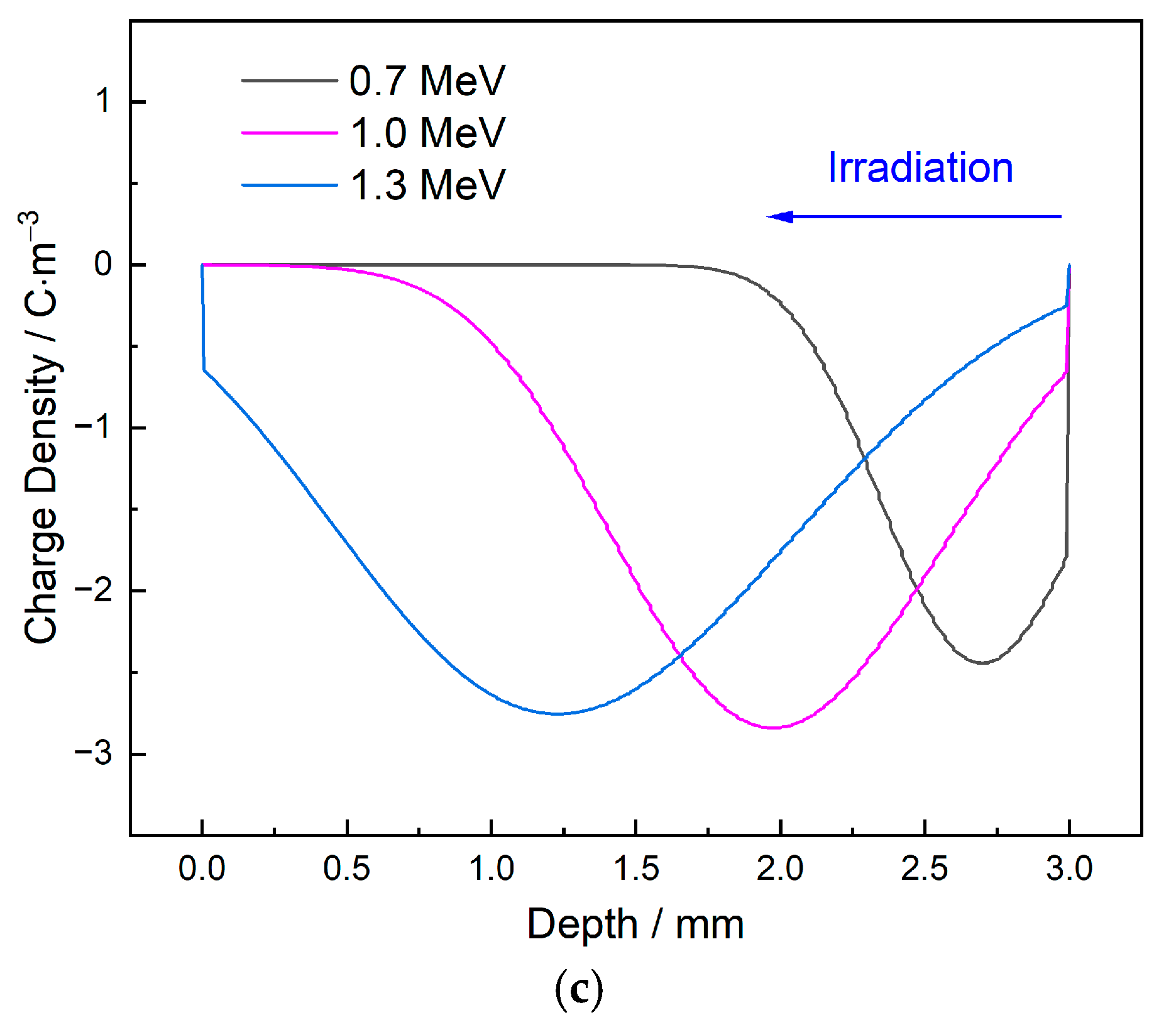
3.1.2. Deposition Charge Distribution Based on Joint Simulation Method

According to Section 2.3, the simulation model of PI under high-energy electron radiation is shown in Figure 7.
To compare with the experiment, a 0.5 mm thick aluminum shielding layer was set in the simulation model due to the in-situ PEA configuration. In the simulation, the energies of the high-energy electrons were also set to 0.7 MeV, 1.0 MeV and 1.3 MeV, respectively, and the number of radiated electrons was 108. The size of the PI sample was 10 mm × 10 mm × 3 mm, and the mesh grid size was 0.1 mm × 0.1 mm × 0.05 mm. Detailed physical parameters are shown in Table 1.
Then the charge deposition rate in the PI was obtained, as shown in Figure 8. The upper and lower surfaces of the sample were further grounded in COMSOL calculation to obtain the deposited charge density according to Equations (6)–(8).

3.1.3. Comparative Analysis of Charging Characteristics under High-Energy Electron Radiation

In addition to the above in-situ measurement method and the joint simulation calculation method, the empirical equation could also be used. The maximum penetration depth of high-energy electron in a plate-like dielectric with infinite thickness can be expressed by Weber’s semi-empirical equation [31].
R = 0.01 α E 0 ρ 1 β 1 + γ E 0
where R is the maximum range of the incident electron in the medium, m; α, β, γ are 0.55 g/cm2·MeV−1, 0.9841, 3 MeV−1, respectively; E0 is the incident energy of the incident electron, MeV; ρ is the density of the dielectric material, g/cm3. The deposited charge density at unit depth per unit time was as follows:
d Q ( x , t ) d t = 14.42 x 3 R 4 j 0 ( 1 η ) exp 3.605 ( x R ) 4
where dQ(x,t)/dt is the deposition charge density per unit time, C/(m3·s); j0 is the current density of electrons, A/m2; the value of the backscattering system η is about 0.1; x is the depth of the electron, m. The charge deposition of the sample can be calculated by substituting Equation (13) into Equation (14). In the calculation, the high-energy electrons passing through a 0.5 mm thick aluminum sheet were also considered.
The charge deposition obtained by the three different methods was compared in Figure 9 with detailed data shown in Table 2.
Table 2 shows a good correspondence among experimental measurement, simulation calculation and theoretical calculation in terms of penetrating depth. Only at 1.3 MeV, the simulation result has a large deviation, which might be due to the inaccuracy of peak in the relatively flat charge distribution. In the peak value of charge density, the results under the three methods are slightly different, and the following analysis is made:
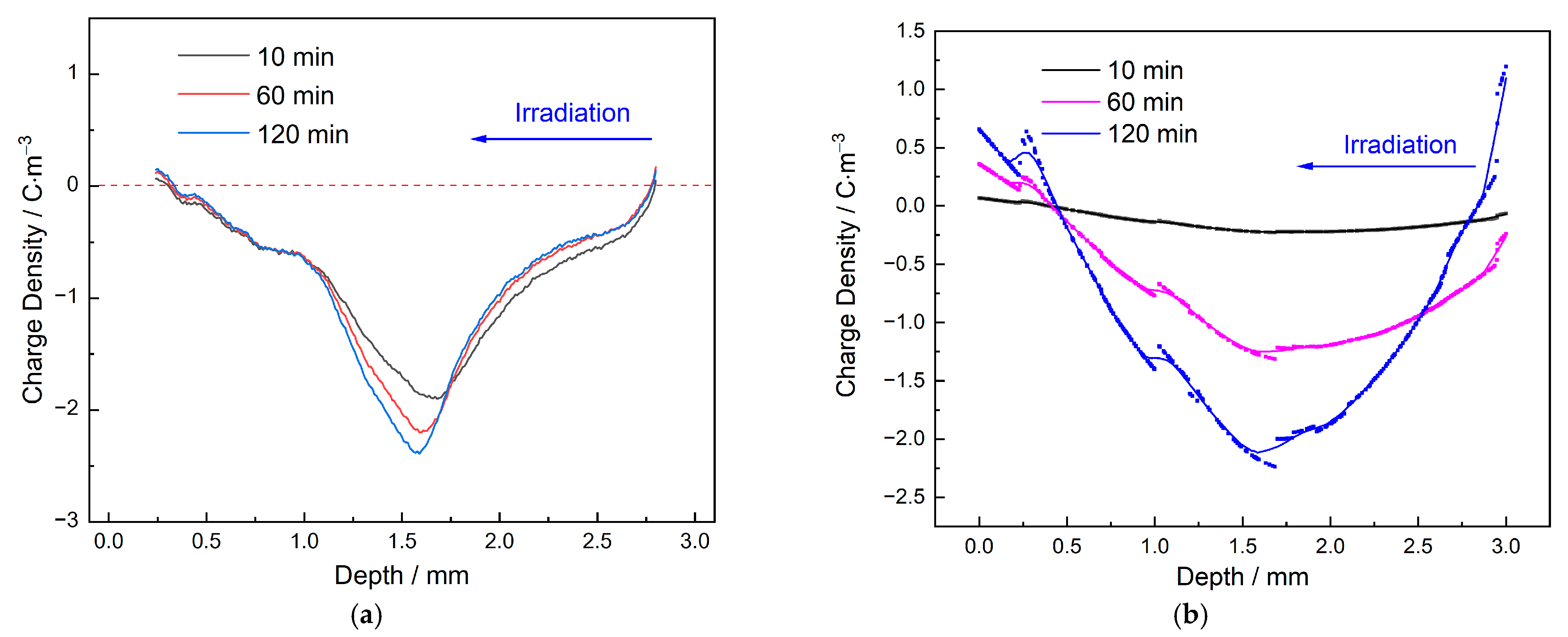
  • In the theoretical calculation, the peak value under the three groups of energies is similar. First, there is a certain deviation in the theoretical empirical equation; in particular, the parameters in Equation (13) have a great influence on the results. On the other hand, in the theoretical calculation, the grounding of the sample on both sides, together with the release of the deposited charge, are not considered. However, theoretical calculation still has a certain reference for the depth of charge deposition.
  • In the simulation method, the charge transportation to the ground through bulk conduction is considered with constant charge injection. Therefore, the overall charge amount in the sample will be equal under the same radiation time, and thus the area enclosed by the horizontal axis and charge density curve are almost the same under three energies in the simulation calculation. However, the measurement results of the total charge amount among the three energies show an obvious difference, which may be due to the more intense charge release process caused by the higher electric field near the grounded electrode.
In general, the deposited charge distribution inside PI under different energies of electron radiation obtained by experimental measurement and simulation calculation, whether the charge position or the density have a certain consistency.

3.2. Internal Charging under Different Radiation Time

The electron radiation time was changed while we maintained the other configuration; the deposited charge of the same PI plate sample was performed. The beam density was 50 pA/cm2, with an energy of 1.0 MeV. The deposited charge distribution was obtained when the radiation time was 10 min, 60 min and 120 min, as shown in Figure 10a.
From Figure 10a, with the increase in radiation time, the peak value of charge density increases gradually, and the position of peak charge density is basically unchanged. Simultaneously, the joint simulation method of Geant4 and COMSOL was used to obtain the deposited charge densities under the same condition, and the results are shown in Figure 10b with details in Table 3.
Under the conditions of different radiation time, the penetrating depth of the deposited charge has a good correspondence between the experiment and the simulation, but there is a certain difference in the peak value of the charge density. Supposing the internal electric field strength of the PI remains low level during the radiation and the σRIC is invariant over radiation time, the charge release rate through conduction should be constant. Then, the total charge amount inside the PI should be proportional to the radiation time, and the simulation result basically satisfies this law. However, the experimental results are obviously larger in the short radiation time but with a good agreement with the simulation in long radiation time, indicating that the bulk conductivity of the PI is still low in the short radiation time. In general, the simulation results are in good agreement with the experimental measurement under different radiation time.

4. Evaluation of Internal Discharging under High-Energy Electron Radiation

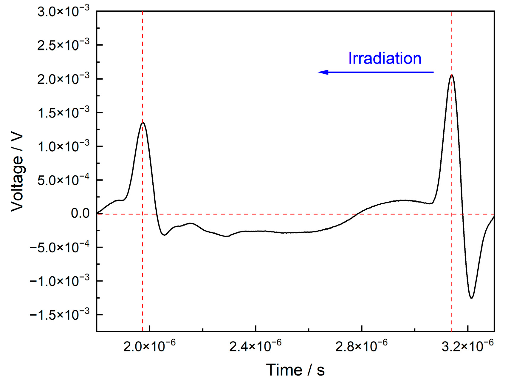
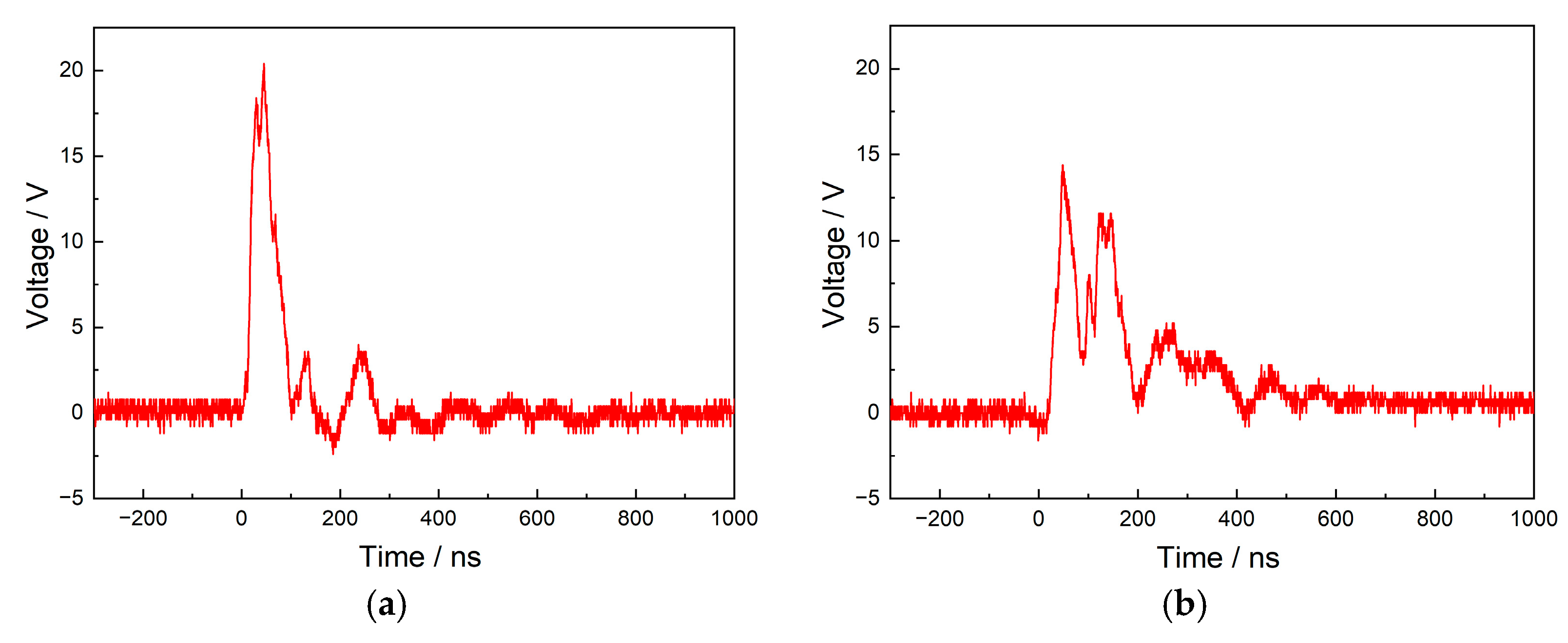
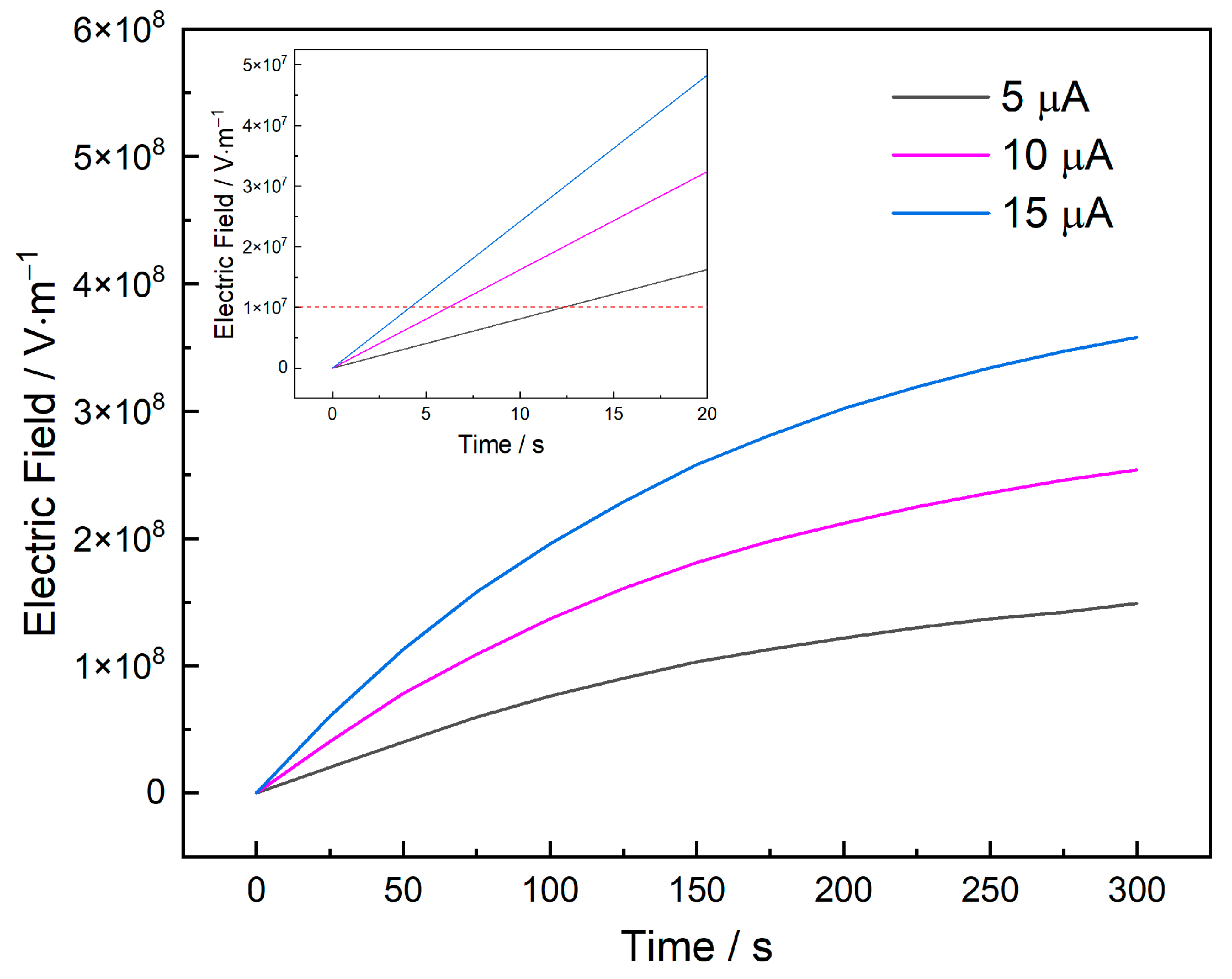
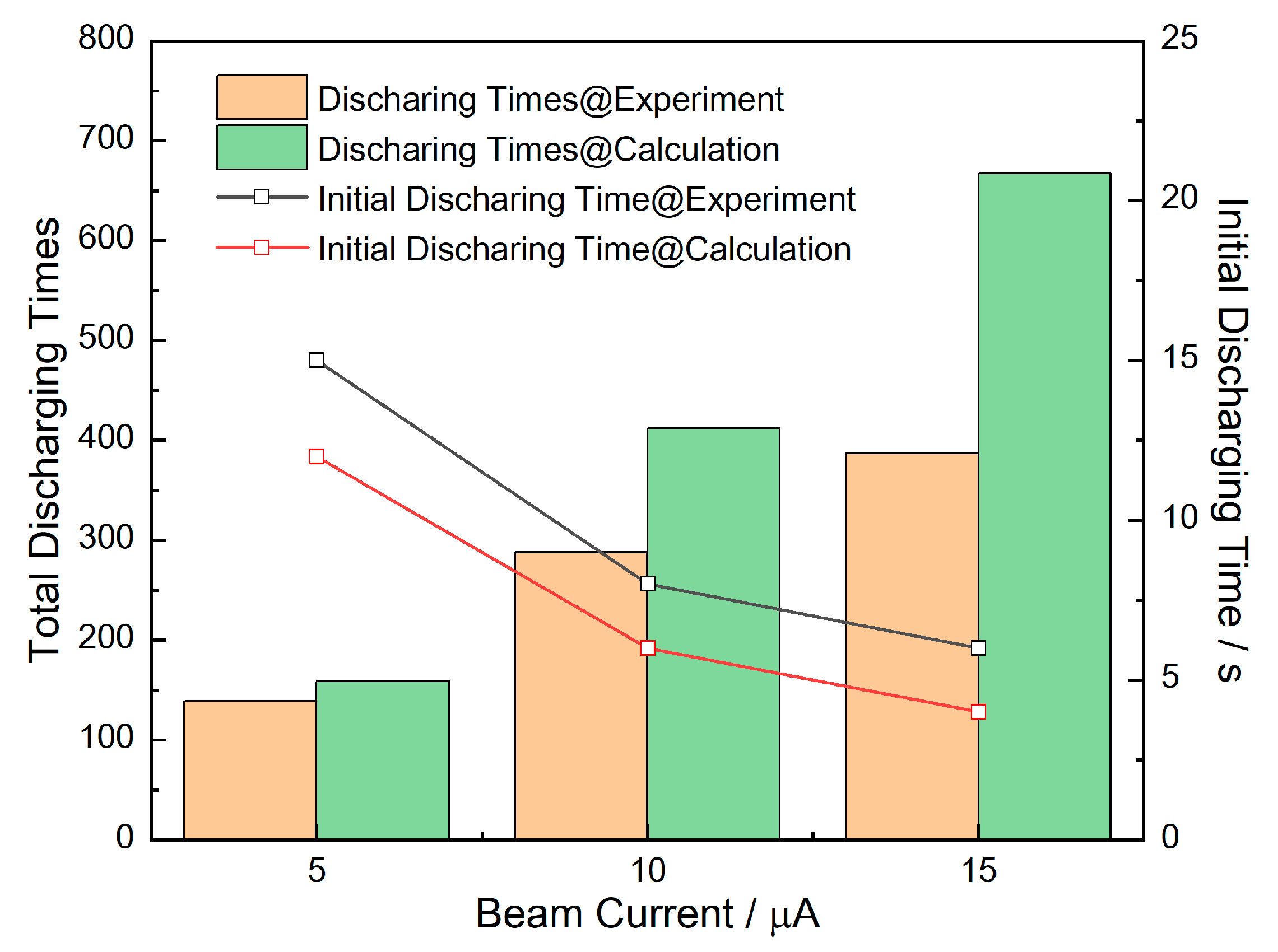
4.1. Experiment Result of Discharging Evaluation

Through the ESD testing platform under the high-energy electron radiation in Section 2.2, the PI sample with a diameter of 10 mm and a thickness of 1 mm was tested. The radiation electron energy was 0.3 MeV and the beam current was 5 μA, 10 μA and 15 μA, respectively, for 20 min. Typical ESD waveforms are shown in Figure 11.
In Figure 11a, the typical ESD waveform is a narrow discharge pulse with a pulse width of about 100 ns, and the pulse rising time is less than 20 ns. There will be a damped oscillation that gradually decays to zero. However, due to the inhomogeneity of the material, the disturbance of the high-energy electron generator and the multi-point discharge, the ESD waveform has poor repeatability and even waveform bifurcation appears, as shown in Figure 11b. Through plenty of ESD experiments and statistical analyses, the average discharging duration is about 200 ns, and the average single discharging quantity is about 1.0 × 10⁻⁶ C, with a relative error ±30%. During 20 min of electron radiation, the total times of discharging and the initial discharging time of PI under three groups of beam current were recorded, as shown in Table 4.

4.2. Simulation Results of Discharging and Comparative Analysis

Furthermore, the simulation method was used to evaluate the ESD characteristics under high-energy electron radiation, so as to verify the effectiveness of the evaluation method. According to the experimental setup in Section 4.1, we established the corresponding radiation simulation model, as shown in Figure 12.
Through the joint simulation method under 0.3 MeV high-energy electron radiation, the internal electric field distribution of PI sample with a diameter of 10 mm and a thickness of 1 mm was obtained under three beam currents of 5 μA, 10 μA and 15 μA. The internal maximum electric field strength is shown in Figure 13.
According to the guideline of the spacecraft protection manual [13], the ESD threshold of the dielectric is generally 2 × 10⁷ V/m, and in some more severe occasions, 1 × 10⁷ V/m is used for internal electric field risk assessment. Here, we chose 1 × 10⁷ V/m as the threshold electric field strength. From the simulation results in Figure 13, it can be obtained that the initial discharging time under the three beam currents, namely the maximum electric field strength equal to threshold value for the first time, is 13 s, 6 s and 4 s, respectively. The result is in good agreement with the experimental results in Table 4.
Through the simulation method, we further analyze the total ESD times during 20 min radiation. According to the beam current, the corresponding beam current densities are 3.04 × 10⁻⁵ A/m2, 6.08 × 10⁻⁵ A/m2 and 1.51 × 10⁻⁴ A/m2, from which the injected charge amount per unit time, Qprimary, can be calculated. Meanwhile, the mode of charge leakage contains the ESD, the charge release through the intrinsic conductivity, the additional charge release caused by the increased bulk conductance due to high electric field strength and high temperature and additional charge release due to radiation-induced conductance. In addition, backscattered electrons generated by the surface should also be considered. Therefore, the amount of deposited charge, Qtotal, is shown in Equation (15), and each process of charge leakage is analyzed below.
Q total = Q primary Q backscatter Q σ E T Q σ RIC Q ESD
  • Single electrostatic discharging. According to Section 4.1, the average electrostatic discharge quantity QESD per unit time of PI is 1.0 × 10⁻⁶ C. In the experiment, there may be multiple discharges, but the discharge waveform collected by the oscilloscope is regarded as a single discharging;
  • Electron backscattering. Under high-energy electric radiation, the backscattered electron yield of PI is generally about 0.1~0.2, so the Qbackscatter by the surface per unit time should not exceed 10% of the total amount of injected charges;
  • Intrinsic conductance. Since the intrinsic conductivity of PI is extremely low, the amount of charge released by the intrinsic conductivity is almost negligible;
  • High temperature and high-field conductance. Due to the increase in the electric field inside the PI and the influence of the radiant heat, electrostatic discharging effect and the difficulty of heat dissipation in the vacuum environment, the PI may be in a relatively high conductivity during the radiation process. According to Yi’s research [32], considering a condition of 10 kV/mm and 353 K under radiation, the bulk conductivity may conform to the following laws.
    σ T = A k T exp ( E A k T )
    σ E T = σ T 2 + cosh ( β F E 0.5 2 k T ) 3 2 k T e E δ sinh ( e E δ 2 k T )
    where k is the Boltzmann constant, T is the absolute temperature, K; EA is the activation energy of conductivity, A is the coefficient related to the dielectric conductivity at room temperature, E is the electric field strength, V/m; e is the electron charge; βF = (e3/πε)0.5 depends on the permittivity; δ is the jump distance of electrons, generally 1 nm. According to Equations (16) and (17), it is roughly obtained that the bulk conductivity of the PI during the discharge process is about 7.5 × 10⁻¹³ S/m;
  • Radiation-induced conductance. Although the release of the deposited charge in the zone near the back electrode is less affected by high-energy electron radiation, the overall charge transportation in the radiation zone is accelerated, leading to an enhanced charge release. According to Equations (9)–(11), the σRIC tends to rise by 2–3 orders of magnitude relative to the intrinsic conductivity.
Taking into account the above charge injection and charge leakage processes, the quantitative calculation of the internal charge of the PI under high-energy electron radiation can be obtained in Table 5. The symbol (+) in the table represents the charge accumulation process while (−) represents the charge release process.
According to Table 5, under 5 μA beam radiation, the net charge increase in PI dielectric per unit time is 1.34 × 10⁻⁷ C, while the single QESD is 1.0 × 10⁻⁶ C. Since the single discharge time is often less than 200 ns, the ESD is instantaneous, relative to the increase in net charge per unit time. In summary, it can be calculated that the charge deposition inside PI will reach the discharging threshold again after 7.5 s, so that we can quantitatively obtain the estimated total ESD times within the 20 min radiation. Moreover, according to the same calculation method, the total ESD times under the conditions of 10 μA and 15 μA can also be obtained and results are shown in Figure 14.
From Figure 14, the simulated initial discharging time of the PI under different beam currents is basically consistent with experimental results. On the other hand, for total ESD times during the 20 min radiation, the simulation method has a good correspondence with the experiment, especially under the condition of lower beam current. The difference of the discharging times becomes larger when the beam current increases to 15 µA, and the following two points should be further considered. Firstly, in the ESD measurement under larger beam current, there may be micro-discharge processes that are beyond the capture ability of the testing system. In addition, except for single-peak ESD in Figure 11a, there is also multi-peak discharging, such as in Figure 11b. This kind of ESD waveforms might be caused by two time-superimposed discharging at different locations, but they are counted as a single ESD in our experiment. Combining the above two situations, the number of internal discharging obtained in the experiment should be less than that of the simulation.
Through the comparative study on the internal discharging evaluation of PI under high-energy electron radiation, the joint simulation method based on Geant4 and COMSOL is in good agreement with the experimental measurement results. Therefore, the evaluation of the internal charging and discharging of the dielectrics under the orbital radiation spectrum can be carried out based on this method to provide data support for the safe operation of the spacecraft in the future.

5. Conclusions

The internal charging–discharging characteristics of polyimide used in spacecraft was evaluated by experiment and simulation methods under high-energy electron radiation in this work.
The in-site PEA measurement system under high-energy electron radiation was established for evaluating the charging characteristics of thick plate samples of about 3 mm, and the deposited charge distribution could be effectively obtained under different electron energies and radiation time.
The charging characteristics, such as deposited charge positions and charge density, were compared through the in-site PEA experiment and joint simulation method. Overall, the simulation results are in good agreement with that of experimental results under different electron energies and radiation times. The discharging characteristics, such as total discharging times and initial discharging time, were also comparatively evaluated by experiment and joint simulation method. With a good consistency of results, the difference between two methods was analyzed in the perspective of deposited charge leakage. It is validated that both methods can be used for charging–discharging characteristics under certain space environments in future.

Author Contributions

Conceptualization, J.W. and B.Z.; methodology, J.W.; software, Y.Z.; validation, Y.Z., M.H. and P.S.; formal analysis, Y.Z.; investigation, J.W., B.Z. and P.S.; resources, J.W. and Y.Q.; data curation, Y.Q.; writing—original draft preparation, J.W.; writing—review and editing, B.Z.; visualization, J.W.; supervision, J.W.; project administration, J.W.; funding acquisition, J.W. All authors have read and agreed to the published version of the manuscript.

Funding

This research was funded by Shaanxi Provincial Science and Technology Department, grant number 2022JZ-35.

Data Availability Statement

Not applicable.

Conflicts of Interest

The authors declare no conflict of interest.

References

  1. Lai, S.T. Fundamentals of Spacecraft Charging: Spacecraft Interactions with Space Plasmas; Princeton University Press: Oxford, UK, 2012; pp. 205–229. [Google Scholar]
  2. Ji, X.; Li, Y.; Liu, G.; Wang, J.; Xiang, S.; Yang, X.; Bi, Y. A brief review of ground and flight failures of Chinese spacecraft. Prog. Aerosp. Sci. 2019, 107, 19–29. [Google Scholar] [CrossRef]
  3. Frederickson, A.R.; Dennison, J.R. Measurement of conductivity and charge storage in insulators related to spacecraft charging. IEEE Trans. Nucl. Sci. 2003, 50, 2284–2291. [Google Scholar] [CrossRef]
  4. Green, N.W.; Dennison, J.R. Deep dielectric charging of spacecraft polymers by energetic protons. IEEE Trans. Plasma Sci. 2008, 36, 2482–2490. [Google Scholar] [CrossRef]
  5. Fukuma, M.; Maeno, T.; Fukunaga, K.; Nagao, M. High repetition rate PEA system for in-situ space charge measurement during breakdown tests. IEEE Trans. Dielectr. Electr. Insul. 2004, 11, 155–159. [Google Scholar] [CrossRef]
  6. Wang, V.; Wu, J.; Yin, Y. Nanostructures and space charge characteristics of MgO/LDPE nanocomposites. IEEE Trans. Dielectr. Electr. Insul. 2017, 24, 2390–2399. [Google Scholar] [CrossRef]
  7. Rizzo, G.; Romano, P.; Imburgia, A.; Ala, G. Review of the PEA method for space charge measurements on HVDC cables and mini-cables. Energies 2019, 12, 3512. [Google Scholar] [CrossRef]
  8. Enoki, K.; Endo, K.; Miyake, H.; Tanaka, Y. Surface and internal charge measurement in fluorinated polymer irradiated by electron using non-contact type PEA method. IEEJ Trans. Fundam. Mater. 2021, 141, 665–671. [Google Scholar] [CrossRef]
  9. Laurent, C.; Teyssedre, G.; Le Roy, S.; Baudoin, F. Charge dynamics and its energetic features in polymeric materials. IEEE Trans. Dielectr. Electr. Insul. 2013, 20, 357–381. [Google Scholar] [CrossRef]
  10. Griseri, V.; Fukunaga, K.; Maeno, T.; Laurent, C.; Levy, L.; Payan, D. Pulsed electro-acoustic technique applied to in-situ measurement of charge distribution in electron-irradiated polymers. IEEE Trans. Dielectr. Electr. Insul. 2004, 11, 891–898. [Google Scholar] [CrossRef]
  11. Perrin, C.; Griseri, V.; Inguimbert, C.; Laurent, C. Analysis of internal charge distribution in electron irradiated polyethylene and polyimide films using a new experimental method. J. Phys. D 2008, 41, 205417. [Google Scholar] [CrossRef]
  12. Arnaout, M.; Paulmier, T.; Dirassen, B.; Payan, D. Non-contact in-situ pulsed electro acoustic method for the analysis of charge transport in irradiated space-used polymers. J. Electrost. 2015, 77, 123–129. [Google Scholar] [CrossRef]
  13. NASA-HDBK-4002A; Mitigating in Space Charging Effects—A Guideline. NASA: Washington, DC, USA, 2011; p. 33.
  14. Sorensen, J.; Rodgers, D.J.; Ryden, K.A.; Latham, P.M.; Wrenn, G.L.; Levy, L.; Panabiere, G. ESA’s tools for internal charging. IEEE Trans. Nucl. Sci. 2000, 47, 491–497. [Google Scholar] [CrossRef]
  15. Mateo-Velez, J.C.; Theillaumas, B.; Sevoz, M.; Andersson, B.; Nilsson, T.; Sarrailh, P.; Thiebault, B.; Jeanty-Ruard, B.; Rodgers, D.; Balcon, N. Simulation and analysis of spacecraft charging using SPIS and NASCAP/GEO. IEEE Trans. Plasma Sci. 2015, 43, 2808–2816. [Google Scholar] [CrossRef]
  16. Wang, S.; Tang, X.; Wu, Z.; Yi, Z. Internal dielectric charging simulation of a complex structure with different shielding thicknesses. IEEE Trans. Plasma Sci. 2015, 43, 4169–4174. [Google Scholar] [CrossRef]
  17. Sarrailh, P.; Paulmier, T.; Dirassen, B.; Rodgers, D.; Santin, G.; Cipriani, F.; Payan, D. Validation through experiments of a 3-D time-dependent model of internal charging. IEEE Trans. Plasma Sci. 2017, 45, 2566–2572. [Google Scholar] [CrossRef]
  18. Jun, I.; Garrett, H.B.; Kim, W.; Minow, J.I. Review of an internal charging code, NUMIT. IEEE Trans. Plasma Sci. 2008, 36, 2467–2472. [Google Scholar]
  19. Kim, W.; Chinn, J.Z.; Katz, I.; Garrett, H.B.; Wong, K.F. 3-D NUMIT: A general 3-D internal charging code. IEEE Trans. Plasma Sci. 2017, 45, 2298–2302. [Google Scholar] [CrossRef]
  20. Zuo, Y.; Wang, J.; Niu, S.; Wei, Y. Simulations of internal charging effects of artificial radiation belt on dielectric material. IEEE Trans. Nucl. Sci. 2021, 68, 1120–1128. [Google Scholar] [CrossRef]
  21. Tang, X.; Yi, Z.; Meng, L.; Liu, Y.; Zhang, C.; Huang, J.; Wang, Z. 3-D internal charging simulation on typical printed circuit board. IEEE Trans. Plasma Sci. 2013, 41, 3448–3452. [Google Scholar] [CrossRef]
  22. Li, G.; Li, S.; Min, D.; Zheng, X.; Yang, S.; Tang, D.; Shi, L.; Zhao, C. Deep dielectric charging characteristics of ring structure irradiated by energetic electrons. IEEE Trans. Dielectr. Electr. Insul. 2015, 22, 2349–2357. [Google Scholar] [CrossRef]
  23. Wang, J.; Liu, R.; Xiao, R.; Ping, A.; Liu, J.; Zhang, M.; Li, Q. Optimized design of slip ring assembly for aerospace to reduce deep dielectric charging. IEEE Trans. Nucl. Sci. 2022, 69, 915–924. [Google Scholar] [CrossRef]
  24. Wang, X.; Min, D.; Pan, S.; Zheng, S.; Hou, X.; Wang, L.; Li, S. Coupling effect of electron irradiation and operating voltage on the deep dielectric charging characteristics of solar array drive assembly. IEEE Trans. Nucl. Sci. 2021, 68, 1399–1406. [Google Scholar] [CrossRef]
  25. Fukuma, M.; Funo, R.; Murakami, Y.; Nagao, M.; Hozumi, N. Measurement of acoustic property for signal recovery in PEA method. In Proceedings of the 2011 International Symposium on Electrical Insulating Materials, Kyoto, Japan, 7–11 September 2011; pp. 69–72. [Google Scholar]
  26. Hole, S. Behind space charge distribution measurements. IEEE Trans. Dielectr. Electr. Insul. 2012, 19, 1208–1214. [Google Scholar] [CrossRef]
  27. Murkami, Y.; Sugiyama, T.; Kasashima, T.; Nagao, M.; Fukuma, M. Signal recovery of space charge distribution using acoustic property in PEA method. In Proceedings of the IEEE International Conference on the Properties and Applications of Dielectric Materials, Sydney, NSW, Australia, 19–22 July 2015; pp. 1208–1214. [Google Scholar]
  28. Qin, X.; He, D.; Wang, J. Geant4-based calculation of electric field in deep dielectric charging. Acta Phys. Sin. 2009, 58, 684–689. [Google Scholar]
  29. Yuan, Q.; Wang, S.; Huang, X. 3-D simulation of internal dielectric charging characteristics of spacecraft dielectric disc structure. Acta Aeronaut. Astronaut. Sin. 2019, 40, 289–298. [Google Scholar]
  30. Pan, S.; Min, D.; Wang, X.; Hou, X.; Wang, L.; Li, S. Effect of electron irradiation and operating voltage on the deep dielectric charging characteristics of polyimide. IEEE Trans. Nucl. Sci. 2018, 66, 549–556. [Google Scholar] [CrossRef]
  31. Li, S.; Li, G.; Min, D.; Zhao, N. Influence of radiation electron energy on deep dielectric charging characteristics of low density polyethylene. Acta Phys. Sin. 2013, 62, 593–602. [Google Scholar]
  32. Zhong, Y.; Wang, S.; Tang, X.; Wu, Z.; Zhang, C. Computer simulation on temperature-dependent internal charging of complex dielectric structure. Acta Phys. Sin. 2015, 64, 307–315. [Google Scholar] [CrossRef]
Figure 1. Measurement electrode system for space charge distribution under high-energy electron radiation.
Energies 15 06603 g001
Figure 2. In-situ measurement system of space charge distribution under high-energy electron radiation.
Energies 15 06603 g002
Figure 3. Schematic diagram of the space charge waveform recovery process.
Energies 15 06603 g003
Figure 4. ESD testing system under high-energy electron radiation.
Energies 15 06603 g004
Figure 5. Joint simulation method of internal charging based on Geant4 and COMSOL.
Energies 15 06603 g005
Figure 6. Original voltage waveform of in-site PEA method under 1.3 MeV electron radiation.
Energies 15 06603 g006
Figure 7. Geant4 simulation model and radiation process.
Energies 15 06603 g007
Figure 8. Calculation results of charge deposition rate by the joint simulation method under different electron energies: (a) 0.7 MeV, (b) 1.0 MeV, (c) 1.3 MeV.
Energies 15 06603 g008
Figure 9. Evaluation results of internal charging under different electron energy radiation: (a) experimental measurement; (b) simulation calculation; (c) theoretical calculation.
Energies 15 06603 g009aEnergies 15 06603 g009b
Figure 10. Evaluation results of internal charging under different radiation times: (a) experimental measurement; (b) simulation calculation.
Energies 15 06603 g010
Figure 11. Electrostatic discharge waveforms of PI under 0.3 MeV electron radiation: (a) typical waveform; (b) sharp and large bifurcation waveform.
Energies 15 06603 g011
Figure 12. Simulation of electric field strength under 0.3 MeV high-energy electron radiation.
Energies 15 06603 g012
Figure 13. Simulation results of the maximum electric field under the radiation of three electron beam currents at 0.3 MeV.
Energies 15 06603 g013
Figure 14. Comparison of experiment and simulation of discharging characteristics of PI within 20 min of 0.3 MeV electron radiation.
Energies 15 06603 g014
Table 1. Related parameter settings in simulation.
ParameterValue
εr3.45
T293 K
ρ1417 kg/m3
kRIC(T)3.63 × 10⁻¹⁵
Δ(T)0.76
σ03.6 × 10⁻¹⁷ S/m
Table 2. Comparison of experimental and calculated results of charge deposition distribution under different energies.
Penetrating Depth of Peak/mmPeak Value of Charge Density/C·m−3
0.7 MeV1.0 MeV1.3 MeV0.7 MeV1.0 MeV1.3 MeV
Experiment0.51.11.6−1.1−1.4−2.3
Simulation0.41.42.4−2.7−2.2−1.4
Theory0.31.01.8−2.5−2.8−2.6
Table 3. Comparison of experiment and simulation results of charge deposition distribution under different radiation times.
Penetrating Depth of Peak/mmPeak Value of Charge Density/C·m−3
10 min60 min120 min10 min60 min120 min
Experiment1.31.41.4−1.9−2.2−2.4
Simulation1.31.41.4−0.22−1.3−2.1
Table 4. Statistical results of ESD characteristics of PI within 20 min under 0.3 MeV electron radiation.
Beam Current/μATotal Discharging TimesInitial Discharging Time/s
513915
102888
153876
Table 5. Calculation results of charge deposition and release per unit time of PI under 5 μA radiation.
Charge Transportation ProcessEstimated Value/C
Injected charge+2.39 × 10⁻⁷
Backscattered charge−2.39 × 10⁻⁸
Charge leakage by conduction under high temperature and high electric field−5.9 × 10⁻⁸
Charge leakage by radiation-induced conductance−2.2 × 10⁻⁸
Publisher’s Note: MDPI stays neutral with regard to jurisdictional claims in published maps and institutional affiliations.

