Abstract
Modular input-series–output-parallel (ISOP) converters are very suitable for high-voltage and high-power applications. In order to ensure the normal operation of ISOP converters, it is necessary to realize the input-voltage and output-current equalization of each submodule. However, there are few studies on the input-voltage and output-current equalization performance of the ISOP system. In this paper, the input-voltage and output-current equalization characteristics of a Boost + LLC modular ISOP converter are studied based on the small-signal model. In this paper, the small-signal model of an ISOP system is first established, and then the input-voltage and output-current equalization performance of the ISOP system under the condition of inconsistent submodule parameters are analyzed. Finally, simulations and experiments are reported to verify the results. The experimental results show that the ISOP system composed of a Boost + LLC cascaded module has excellent voltage and current self-equalization performance.
1. Introduction
Restricted by the voltage and current levels of power devices, modular ISOP converters have received more and more attention and been increasingly researched for high-voltage and high-power applications such as rail transit [1]. In addition to making low-voltage power devices used in high-voltage situations, a modular ISOP structure also has the advantages of high reliability, low cost, good redundancy and high efficiency [2,3]. The main challenge faced by modular serial–parallel systems is the balanced power distribution among submodules; otherwise, the submodules will be damaged due to overvoltage or over-current [4,5,6]. Because the ISOP submodules of the system have the same input current and output voltage, the normal function of the ISOP system depends on the realization of each module of input-voltage and output-current equalization [2,3,4,5,6], but previously, ISOP equalization has been studied, and the performance of the flow has not been sufficiently analyzed in depth [2].
In [7], the relationship between input voltage and output current equalization of DC-DC ISOP system was given, and points out that once the input voltage equalization is realized among sub-modules, the output current equalization can be automatically realized, and vice versa. They also pointed out that the ISOP system is stable when input-voltage equalization control is adopted, while the ISOP system is unstable when the output-current equalization control strategy is adopted. Therefore, it is more meaningful to study the input-voltage equalization performance of the ISOP system.
Authors of [3,8,9] presented the ISOP system of flyback as a sub-module, and analyzed the voltage equalization effect when the parameters of the sub-module were inconsistent. They pointed out that the voltage equalization effect of the converter in continuous current mode depends on the consistency of the transformer turns ratio [3]. The voltage-equalizing performance in discontinuous current mode depends on the consistency of transformer excitation inductance [8,9]. The authors of [10] studied the ISOP system of a phase-shifted full-bridge converter as a submodule and analyzed in detail the influence of inconsistent submodule parameters on dynamic and steady voltage equalization performance through the small-signal model. The above research provides ideas for research on the voltage and current equalization performance of ISOP systems with different converter topologies.
When the submodule of the DC-DC ISOP system works in DC Transformer (DCT) mode, the ISOP system has the characteristic of automatically realizing input-voltage and output-current equalization [7]. For a DC-DC ISOP system with self-equalizing voltage and current performance, simple common duty cycle control is usually used to achieve the power self-equalization of submodules [3,9,10]. In [3] and [10], self-equalizing ISOP systems using common duty cycle control showed excellent dynamic and steady-state voltage-equalizing performance, so there was no need for an additional voltage-equalizing circuit or voltage-equalizing control strategy [11].
In this paper, the voltage- and current-sharing characteristics of an ISOP system composed of a Boost + LLC cascaded module are studied. Then, the performance of the input-voltage and output-current equalization of the ISOP system under the condition of inconsistent submodule parameters is studied. Finally, it is verified by simulations and experiments.
2. Small-Signal Model Analysis of ISOP System
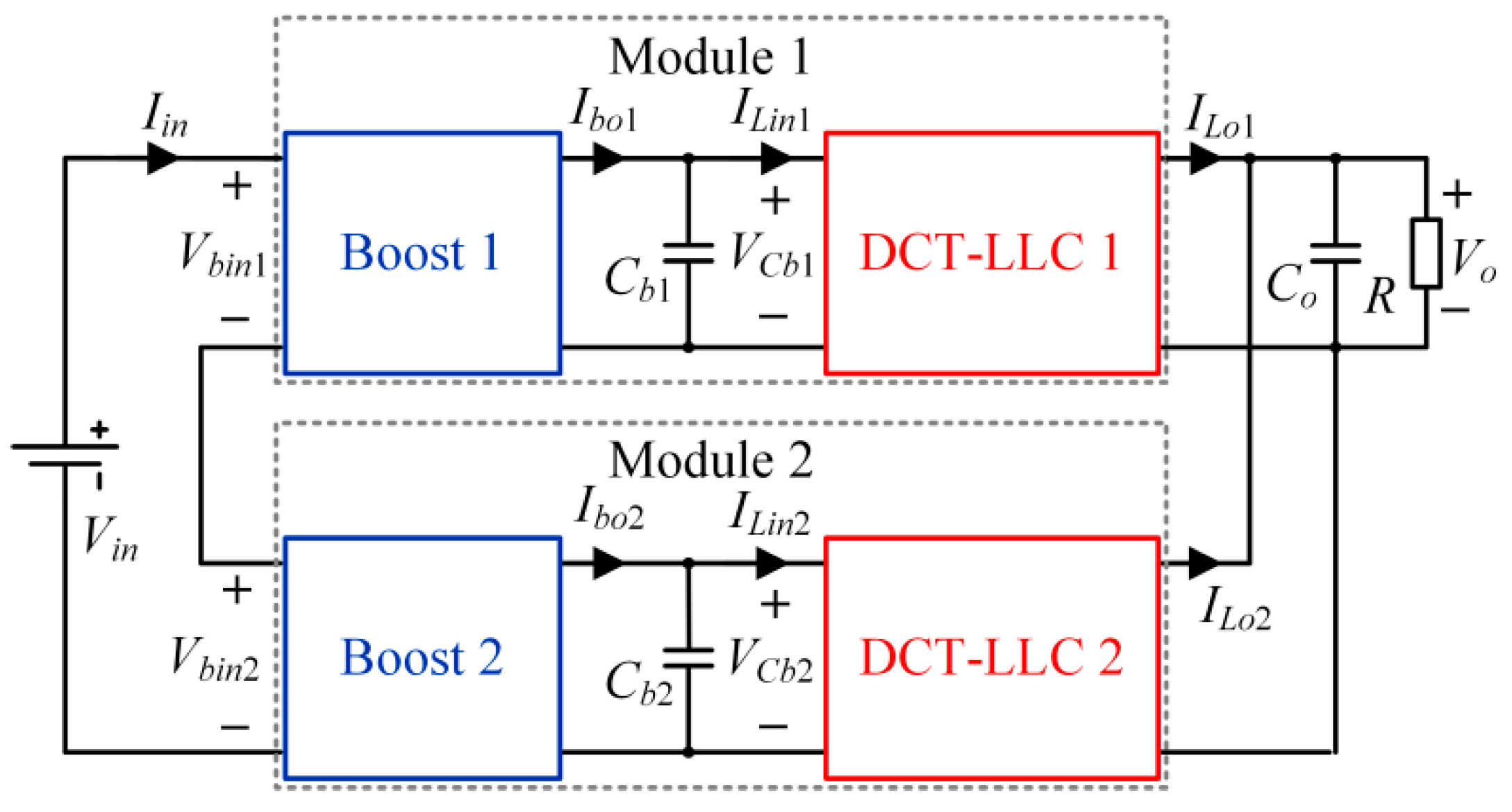
Figure 1 shows an ISOP system topology consisting of two Boost + LLC modules. In order to improve the power density and efficiency of the system, the full-bridge LLC resonant converter is used as a DCT, and its switching frequency and duty cycle are fixed, mainly playing the role of an isolator and transformer. The Boost converter is responsible for regulating the input voltage of LLC; because of the input side of the two Boost converter series, staggered control is used to reduce the Boost inductance. The input-voltage level of the system is high. If two sets of Boost modules are used in series, the voltage stress borne by the MOSFET of the Boost can be reduced. A MOSFET with a lower voltage level is used in this section, and the small-signal models of the interleaved Boost converter and full-bridge LLC resonant converter are analyzed.
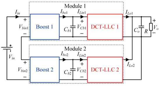
Figure 1.
Topology of the ISOP system composed of Boost + LLC cascaded modules.
2.1. Small-Signal Model of Interleaved Boost Converter
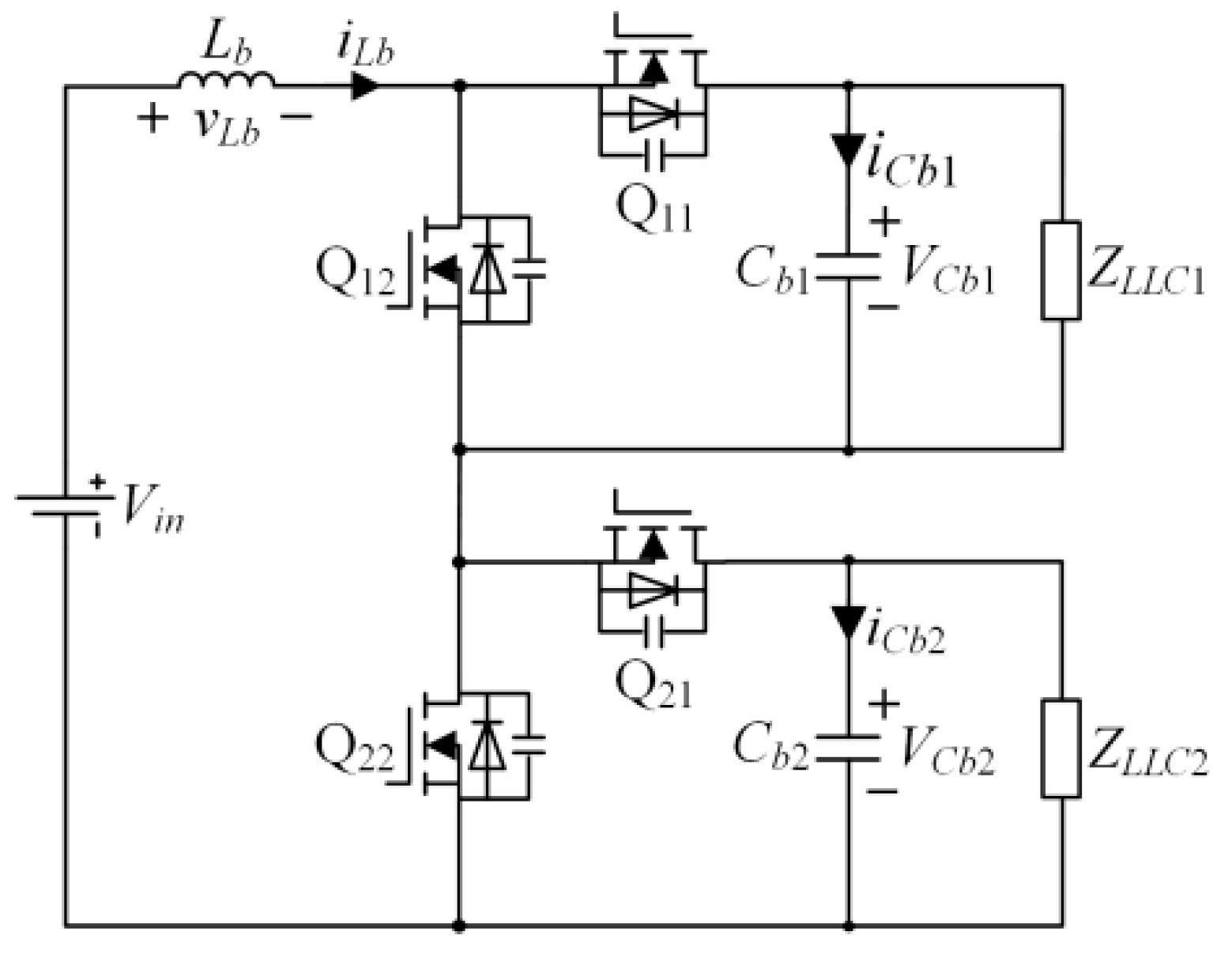
The equivalent circuit of the interleaved Boost converter is shown in Figure 2, where Vin is the input voltage, and Vcb1 and Vcb2 are the output voltages of the two Boost converters, respectively. As the Boost inductors of the two converters are in series, they are regarded as the equivalent inductor Lb in the analysis, while vLb and iLb are the voltage and current of the equivalent inductor Lb, respectively. ZLLC1 and ZLLC2 are the input impedances of two full-bridge LLC resonant converters.

Figure 2.
Equivalent circuit of interleaved Boost converter.
The interleaved Boost converter works in PWM mode; Q11 and Q21 are only used as diodes, while Q12 and Q22 are interleaved with a phase difference of 180 degrees, and the state-space averaging method is used to conduct small-signal modeling [12]. The state equation of the small-signal model can be obtained as
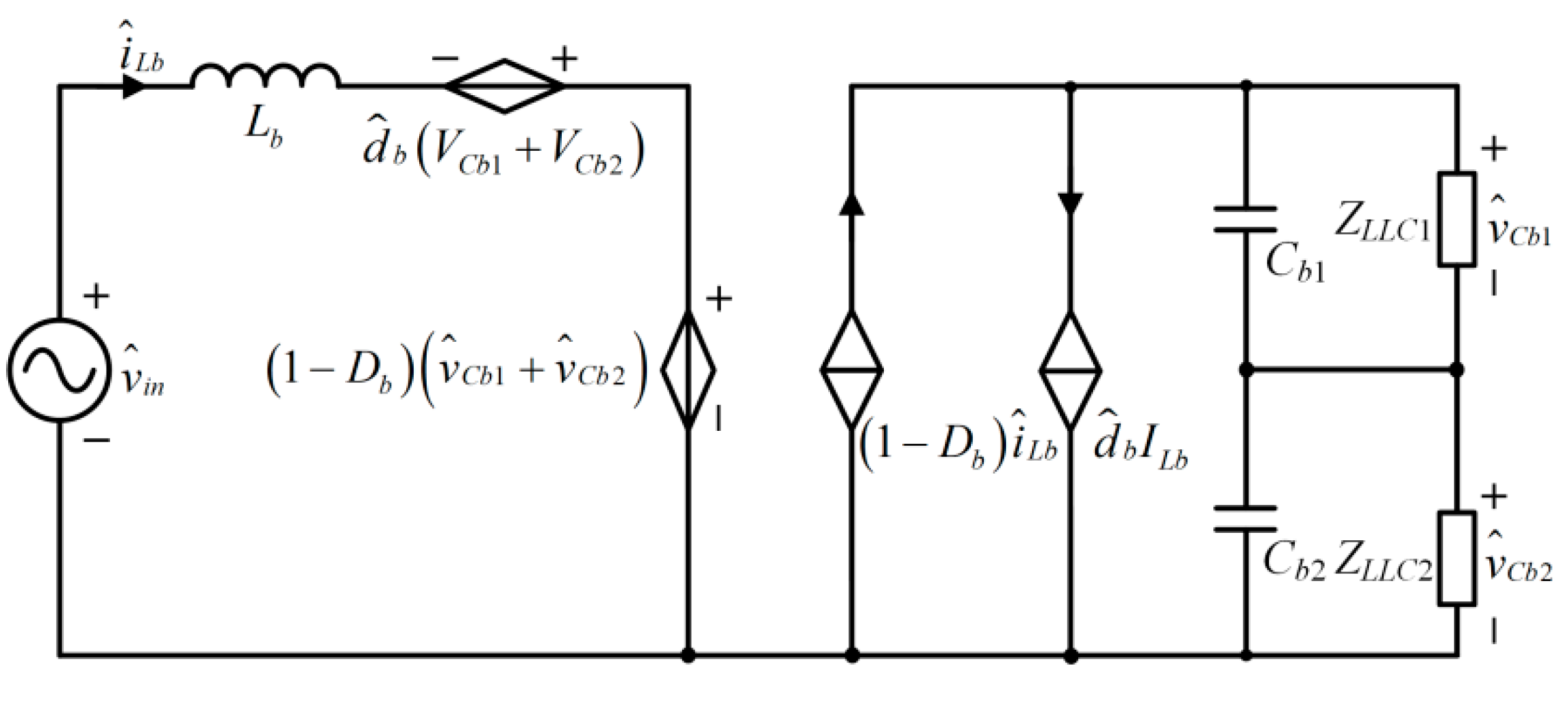
According to (1), the equivalent circuit of the small-signal model of the interleaved Boost converter can be obtained, as shown in Figure 3.
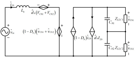
Figure 3.
Small-signal equivalent circuit model of interleaved Boost converter.
2.2. Simplified Small-Signal Model for Full-Bridge LLC Resonant Converter
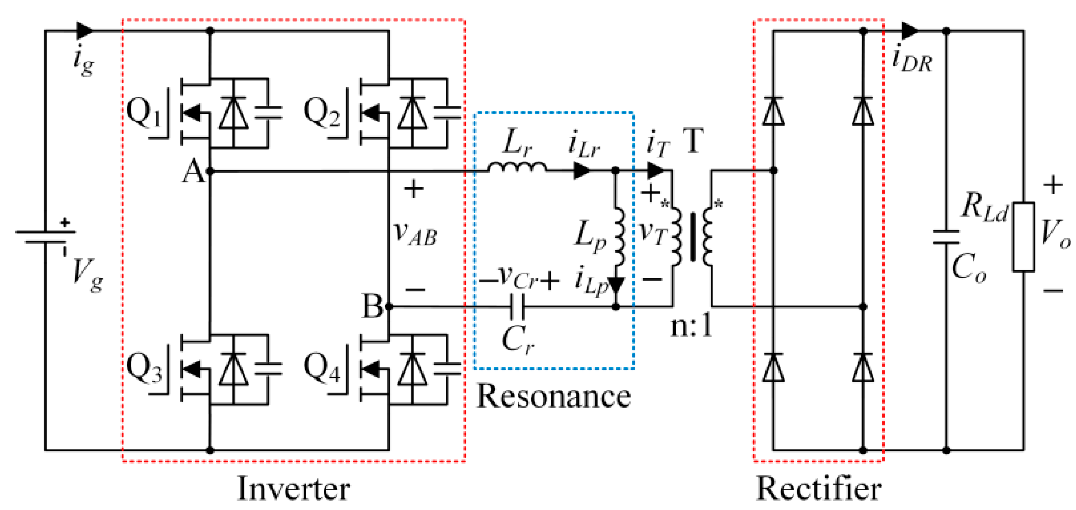
The circuit topology of the full-bridge LLC resonant converter is shown in Figure 4. Cr is the resonant capacitor, Lr is the series resonant inductor, and Lp is the parallel resonant inductor. T is an ideal transformer, whose ratio between the primary and secondary sides is n:1, whose output filter capacitance is Co and whose RLd is the equivalent load. vg and ig are the input voltage and current, respectively; vCr and iLr are the resonant capacitor voltage and resonant current, respectively; iLp is the parallel resonant inductance current; vT and iT are the voltage and current of the original side of the transformer; and iDR is the rectifier bridge output current.
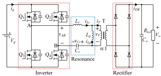
Figure 4.
Topology of Full-Bridge LLC Resonant Converter.
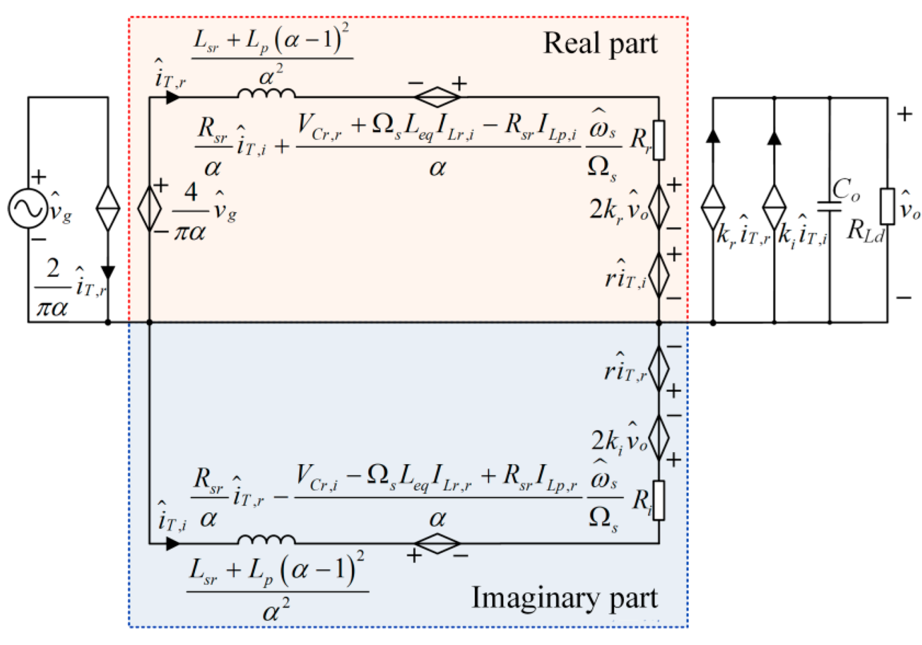
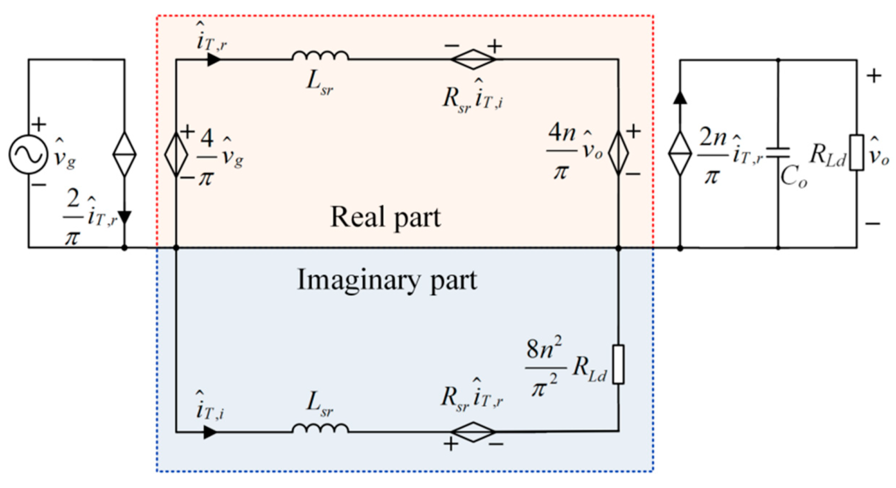
The LLC resonant converter has two resonant states depending on whether Lp participates in resonance or not. The seventh-order small-signal model of the LLC resonant converter can be obtained by using an extended description function method for small-signal modeling [13]. As the frequency of the disturbance signal is far lower than the switching frequency, the series resonant inductor, resonant capacitor and parallel resonant inductor in the seventh-order small-signal model can be combined [14], and the third-order small-signal model of the full-bridge LLC resonant converter is obtained, as shown in Figure 5.
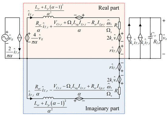
Figure 5.
Third-order small-signal model of full-bridge LLC resonant converter.
Leq is the equivalent resonant inductance, and Lsr and Rsr are the equivalent inductance and complex impedance of the combined branch, which can be written as
where ωs = 2πfs, which is the switching angular frequency, and Ωs is the steady switching angular frequency; the other parameters in Figure 5 are as follows:
ωn = ωs/ωr, ωr = 2πfr, and Rac = 8n2RLd/π2, which is the equivalent load converted to the original side of the transformer. γ is expressed as
In this paper, the full-bridge LLC resonant converter is used as the DCT. In order to ensure good soft-switching performance and DC voltage gain stability, the switching frequency fs is slightly smaller than the resonant frequency fr of Lr and Cr, and Lp is much larger than Lr [15]. According to the above two characteristics, the following formula can be established:
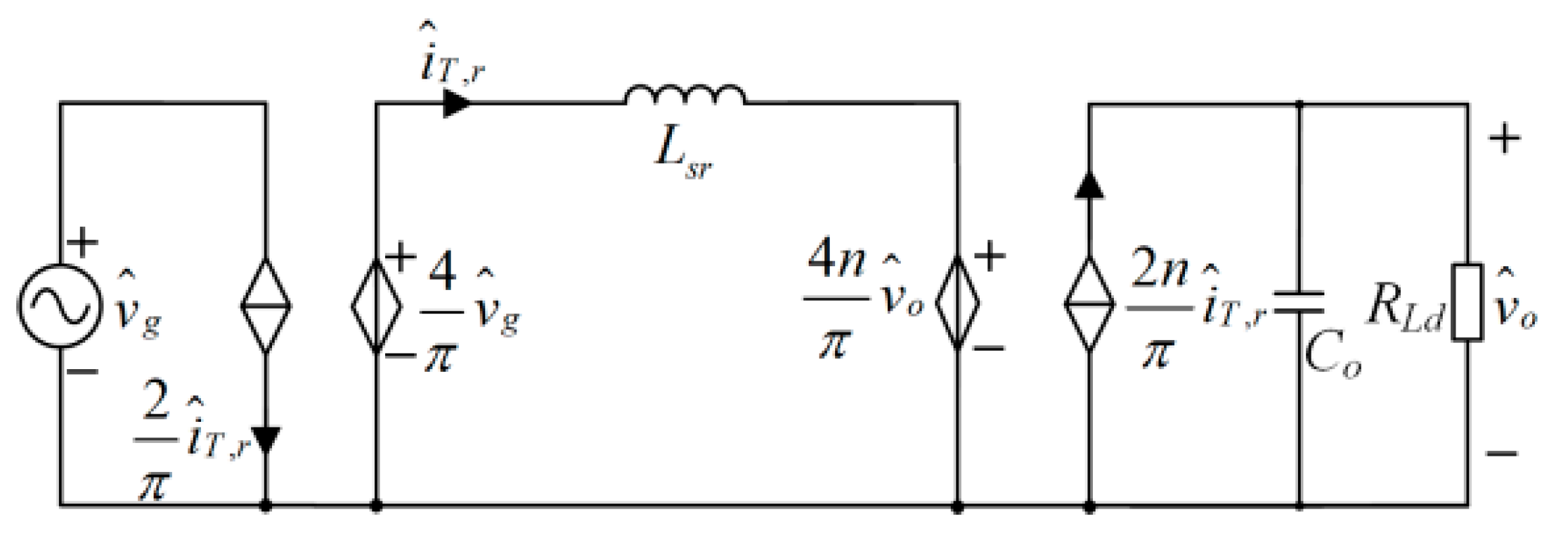
By combining (5) with (8), we can obtain α ≈ 1, γ >> 1, Rr ≈ 0, R ≈ Rac, r ≈ 0, kr ≈ 2n/π and ki ≈ 0. Because the switching frequency is fixed, the part of the small-signal model related to the switching frequency disturbance can be eliminated. To sum up, the small-signal model shown in Figure 5 can be simplified, and the simplified third-order small-signal model is shown in Figure 6.
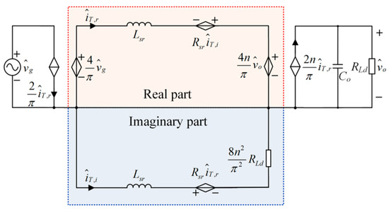
Figure 6.
Simplified third-order small-signal model.
In Figure 6, the loop of the imaginary part satisfies KVL, and the following formula can be established:
Substituting the above equation into the real part loop in Figure 6, we obtain:
Equation (10) shows that the current control-voltage source of the real part of the loop in Figure 6 can be replaced by impedance Zcs(s). It can be seen from (4) and (8) that Zcs(s) ≈ 0 is also valid. After Zcs(s) is substituted into Figure 6, the real part of the small-signal model is no longer coupled with the imaginary part. After the imaginary part is separated, the simplified second-order small-signal model of the full-bridge LLC resonant converter in DCT mode can be obtained, as shown in Figure 7.
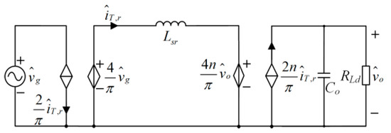
Figure 7.
Second-order small-signal model of full-bridge LLC resonant converter.
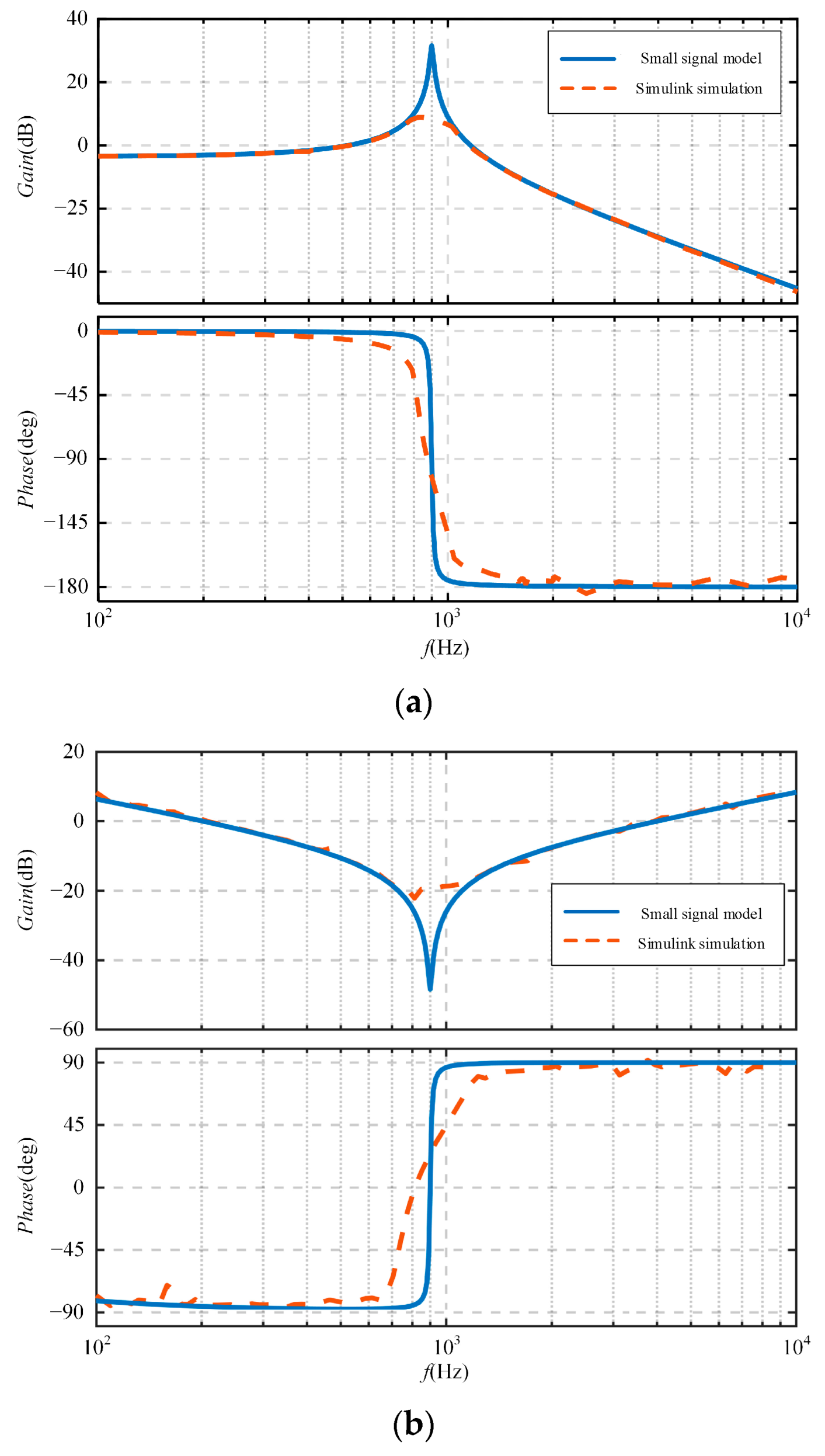
According to Figure 7, the input impedance and voltage transfer function of the full-bridge LLC resonant converter when used as the DCT are shown in (11) and (12), respectively.
Figure 8 shows the Bode diagram of the voltage transfer function and input impedance, including the Bode diagram obtained from the simplified second-order small-signal model and Simulink software simulation. It can be seen that the Bode diagram of the simplified small-signal model transfer function is in good agreement with the simulation results, which proves the accuracy of the simplified small-signal model of the full-bridge LLC resonant converter.
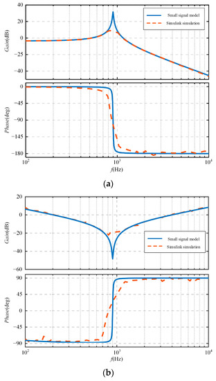
Figure 8.
Bode plots of full-bridge LLC resonant converter. (a) Bode diagram of voltage transfer function; (b) Bode diagram of input impedance.
3. Pressure and Current Equalization Performance Analysis of ISOP System
This section first analyzes the realization mechanism of input voltage and output current equalization of an ISOP system composed of Boost + LLC cascaded modules. Then, based on the small-signal model of the ISOP system, the performance of voltage and current equalization in the case of inconsistent submodule parameters is analyzed.
3.1. Mechanism of Pressure and Flow Equalization in ISOP System
In Figure 1, according to the power conservation of each converter, the following can be obtained:
The two Boost converters adopt interlaced control and have the same duty cycle. Then,
where Vbin1 and Vbin2 are the input voltages of the two Boost converters, VCb1 and VCb2 are the output voltages, ILo1 and ILo2 are the output currents of the two LLC resonant converters, ηb1 and ηb2 are the efficiencies of the two Boost converters, and ηL1 and ηL2 are the efficiencies of the two LLC resonant converters.
Since the efficiency of module 1 is basically the same as that of module 2, it can be considered that ηb1 =ηb2 and ηL1 = ηL2, and substituting them into (13) and (14), the following can be obtained:
This shows that, for the ISOP system constituted by Boost + LLC cascaded modules, as shown in Figure 1, once the output voltage of Boost converter equalization is realized, input-voltage equalization and output-current equalization will be realized automatically [6,16]. Therefore, the output-voltage equalization performance of the Boost converter is mainly analyzed next.
3.2. Analysis of Voltage Equalization Performance of Intermediate DC Bus
To analyze the output-voltage-sharing characteristics of the Boost converter, the transfer function G(s) is constructed as follows:
According to the small-signal model established in II, the following can be obtained:
Substituting (11) into (17), we obtain:
Among them,
Among them, ∆Cb = Cb2−Cb1, ∆Lsr= Lsr1−Lsr2 and ∆n2= n12−n22; ∑Cb = Cb2 + Cb1, ∑Lsr= Lsr1 + Lsr2 and ∑n2= n12 + n22.
3.2.1. Steady-State Pressure Equalization Performance Analysis When Submodule Parameters Are Inconsistent
According to (18), the steady-state output voltage of the Boost converter meets (21); that is, the steady-state voltage-sharing performance only depends on the transformer ratio of the two LLC resonant converters, and the output voltage of the Boost converter corresponding to the module with a larger ratio will be larger.
It is worth noting that, in fact, the error of the transformer ratio is within ±1%. According to (21), the absolute value of the output-voltage difference of the Boost converter is less than 2% of the sum of the two, even if n1 and n2 have a maximum error of +1% and −1%, respectively. Therefore, under steady-state conditions, the ISOP system shown in Figure 1 shows the excellent self-equalizing performance of the output voltage of the Boost converter [17].
3.2.2. Dynamic Pressure Equalization Performance Analysis When Submodule Parameters Are Inconsistent
It can also be seen from (18) that the inconsistent parameters of the submodules will affect the dynamic voltage equalization performance of the system. The following analysis studies the differences between vCb1 and vCb2 in the case of Cb1≠Cb2, Lsr1≠Lsr2 and n1 ≠ n2. The standard circuit parameters of the ISOP system are given in Table 1.

Table 1.
Standard circuit parameters of the ISOP system.
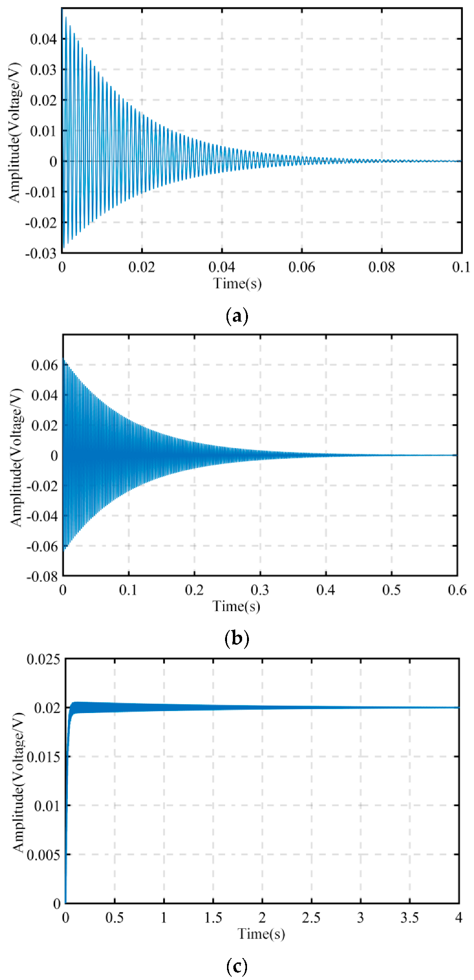
Firstly, only Cb1≠Cb2 is considered. Figure 9 shows Cb1 and Cb2 + 5% and −5%, respectively. When the maximum error of G(s) of the step response occurs, as can be seen in the diagram, the maximum |vCb1(t)-vCb2(t)| value appears at t = 0 + time, (22) can be obtained according to the initial value theorem, then in the dynamic process, the maximum difference in the intermediate bus voltage is proportional to ∆Cb. According to the final-value theorem, (23) is established, and it can be seen that the voltage difference of the intermediate bus in the steady state is independent of ∆Cb.
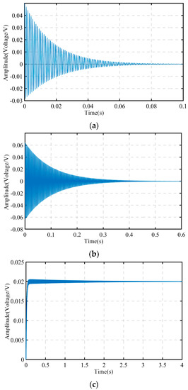
Figure 9.
Step response of G(s) under inconsistent sub-module parameters of different (a) Cb, (b) Lsr, and (c) n.
Next, only Lsr1≠Lsr2 is considered. According to (3), the value of Lsr depends on Lp and Lr. Figure 9b shows Lsr1 and Lsr2 + 10% and −10%, respectively. When the maximum error of G(s) of the step response occurs, as can be seen in the diagram, the |vCb1(t) − vCb2(t)| maximum also appears at the t = 0+ moment, and when the frequency of vbo satisfies ω2 << k3d/k5d, it can be obtained by (24). In addition, according to the terminal-value theorem, the voltage deviation of the intermediate bus in the steady state is almost independent of ∆Lsr.
Finally, only n1≠n2 is considered. Figure 9c shows the step response of G(s) under maximum ±1% changing of transformer ratios n1 and n2, and (25) can be deduced according to the final value theorem, where |vCb1(t) − vCb2(t)| reaches maximum at the steady state from zero initial value. It can be seen that the mismatch between the transformer ratios of the two groups of modules has no effect on the dynamic voltage-sharing performance, and the voltage deviation of the intermediate bus in the steady state only depends on the inconsistency between the transformer ratios of two group modules and is proportional to ∆n2, which is consistent with the analysis result in Section 3.2.1.
To sum up, the dynamic voltage equalization performance of the intermediate DC bus in the ISOP system is affected by the degree of mismatch between the supporting capacitance of the intermediate bus and the resonant circuit parameters of the two submodules, but the steady-state voltage equalization performance only depends on the degree of inconsistency between the transformer ratios of the two submodules. Thanks to the improvement of transformer manufacturing technology, the transformer ratio error is very small in practical applications, so an ISOP system composed of Boost + LLC cascaded modules has excellent self-voltage-balancing performance.
4. Simulation and Experimental Verification
In order to verify the correctness of the theoretical analysis of ISOP system’s input-voltage and output-current equalization, simulation and experimental verifications were carried out.
4.1. Simulation Verification
The simulation model of the closed-loop control ISOP system was built in MATLAB/Simulink software. According to the maximum error of the actual parameters, the resonance parameters of the support capacitance of the middle bus of the two groups of modules in the simulation model are inconsistent with the transformer ratio.
See Table 2 for specific parameters. In this paper, the load of the converter is a three-phase inverter with a rated capacity of 130 kVA and a charger with a rated power of 20 kW. In order to be consistent with the actual working conditions, a simulation model of the three-phase inverter and the full-bridge DC-DC charger was built as the load of the ISOP system.
Table 2.
Specific simulation parameters.
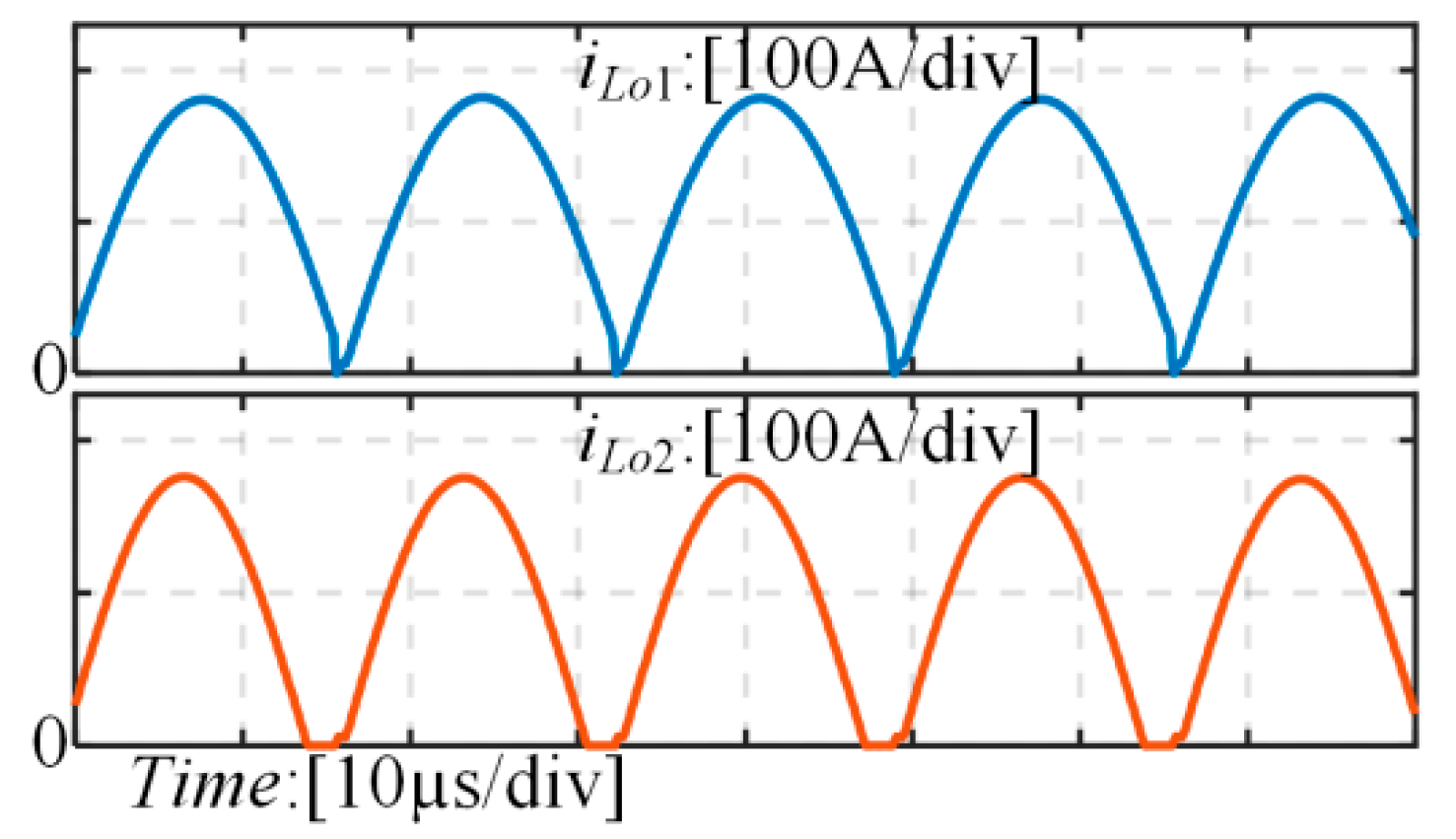
Figure 10 shows the simulation waveform of the input-voltage jump at full load. It can be seen that when vin changes, the deviation between the intermediate bus voltages vCb1 and vCb2 is basically constant and within an acceptable range. The output-current waveforms of the two groups of LLC resonant converters are shown in Figure 11. It can be seen that the output current of the two groups of LLC resonant converters is almost the same. As the resonance parameters of the two group modules are inconsistent and the resonance frequencies are different, the waveforms of iLo1 and iLo2 are not completely consistent.
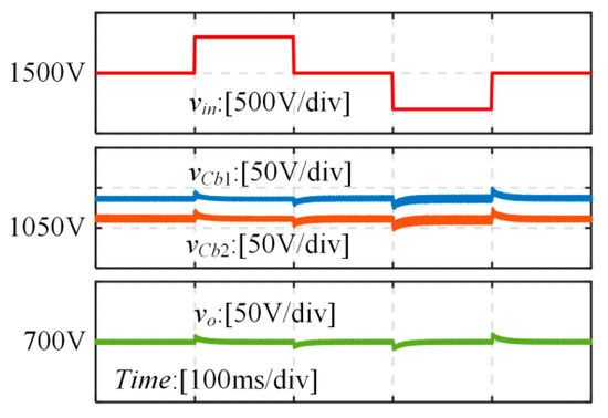
Figure 10.
Simulation waveforms when input voltage changes.
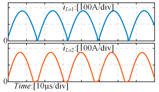
Figure 11.
Steady-state output current of LLC converters.
Figure 12 shows the simulation waveform of the load jump when the input voltage is fixed. The deviation between vCb1 and vCb2 remains constant and within acceptable limits as the load changes. Because fs is slightly smaller than fr, and there is internal resistance in the switching tube and inductor, load changes will affect the voltage gain of the LLC resonant converter, but from 10% load to full load, the changes in vCb1 and vCb2 are not more than 20 V, indicating that the LLC resonant converter plays a beneficial role as the DCT. At the same time, it can be seen that the output current of the two LLC resonant converters is almost the same, but since vCb1 is slightly larger than vCb2, iLo1 will be slightly larger than iLo2.
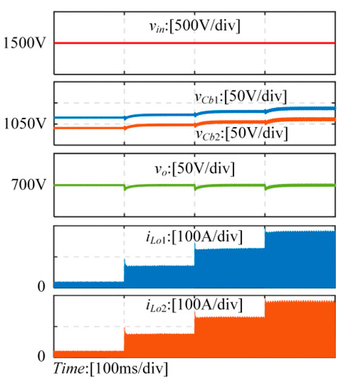
Figure 12.
Simulation waveforms when the load changes.
The above simulation results show that the inconsistent parameters of the submodules have little influence on the voltage-equalizing effect of the intermediate DC bus, and the ISOP system composed of the Boost+ LLC cascaded module has excellent self-equalizing voltage and current performance.
4.2. Experimental Verification
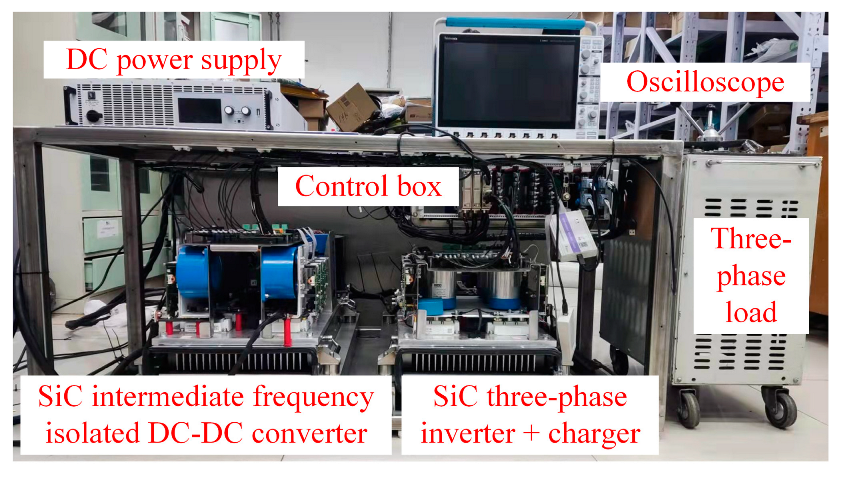
In order to verify the correctness of theoretical analysis and simulation results, an experimental prototype and platform was developed in Figure 13. The rated input voltage was 1500 V and the output power level was 15 kW.
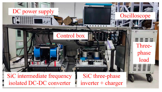
Figure 13.
Experimental prototype and platform.
Due to some error between the actual parameters and the design values, the circuit parameters of the two groups of submodules are not completely consistent. Table 3 shows the actual circuit parameters of the two groups of submodules. Thanks to the current manufacturing technology of magnetic components and capacitors, there is only a slight difference in the parameters of resonant inductance and excitation inductance between the two submodules, and the other circuit parameters have a very good consistency.
Table 3.
Real circuit parameters of the two submodules.
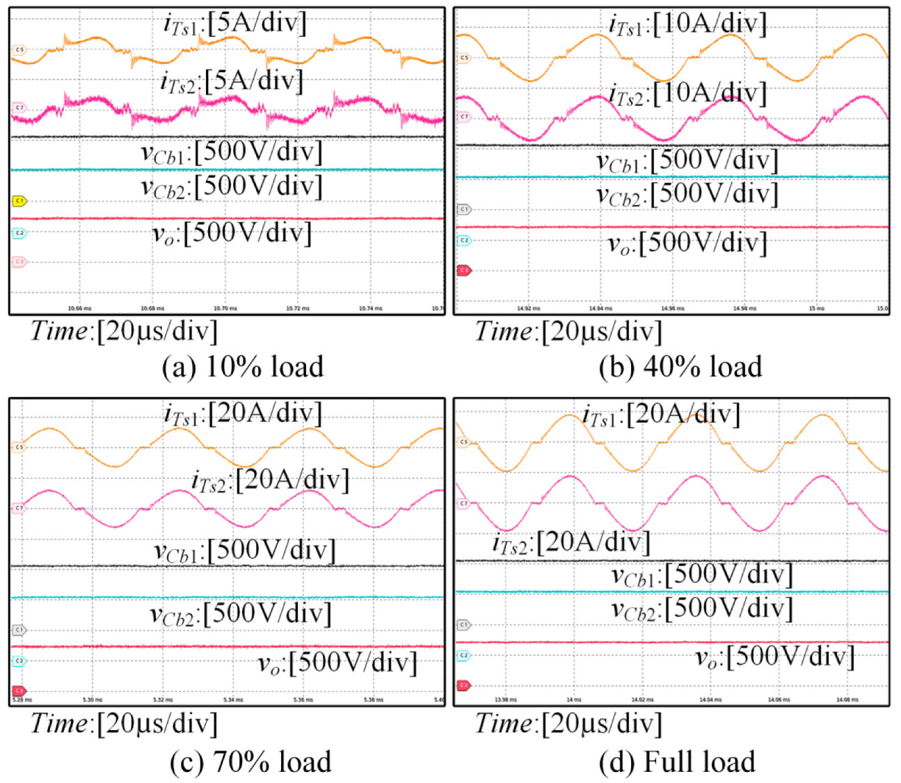
Figure 13 shows the experimental waveforms of the ISOP system under different loads, wherein iTs1 and iTs2 are the output currents of the transformer secondary sides of two groups of submodules, respectively. It can be seen from the figure that under different loads, the output voltage of the ISOP system is stable at 700 V, and the intermediate bus voltage and output current of the two groups of submodules show very good consistency.
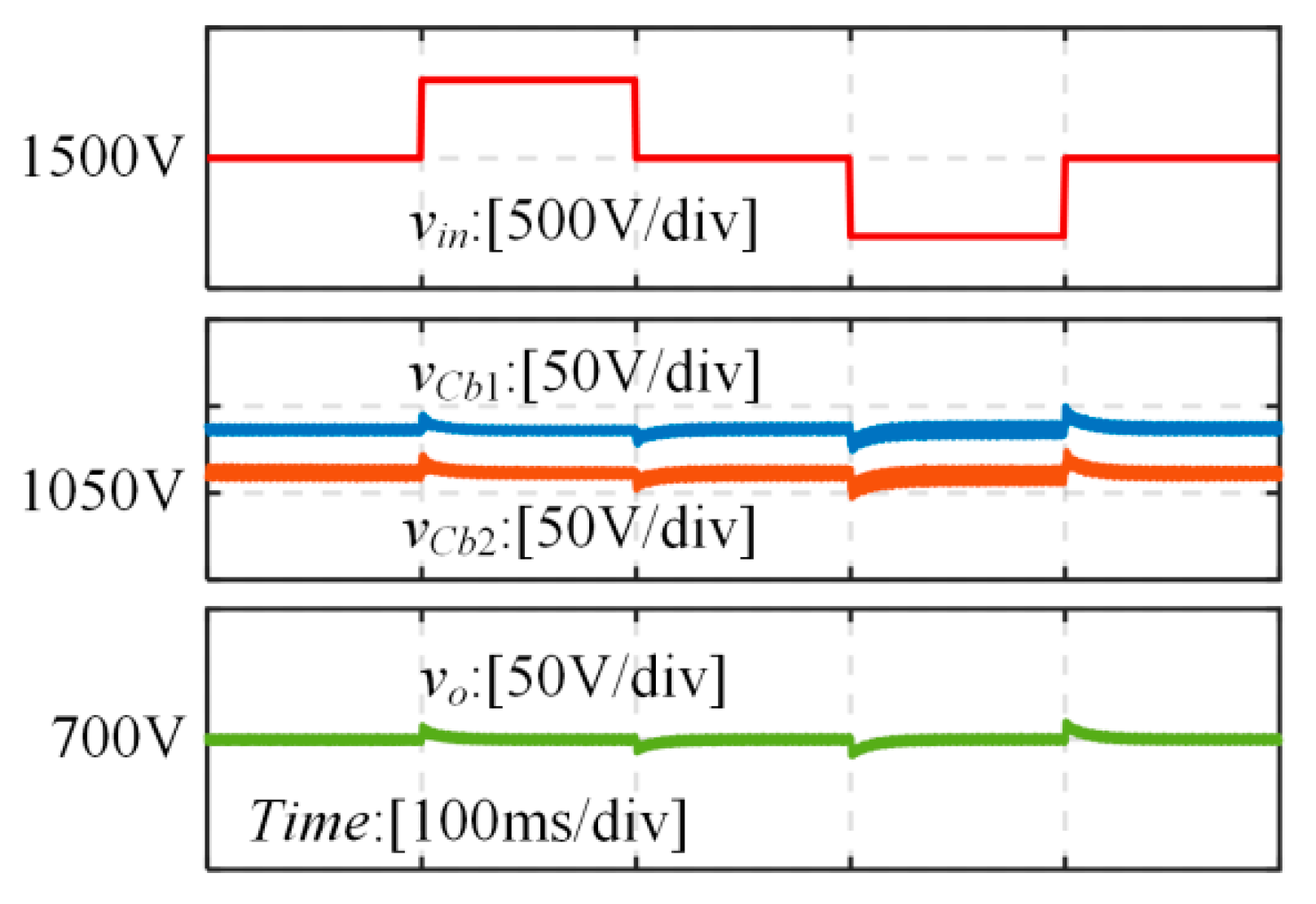
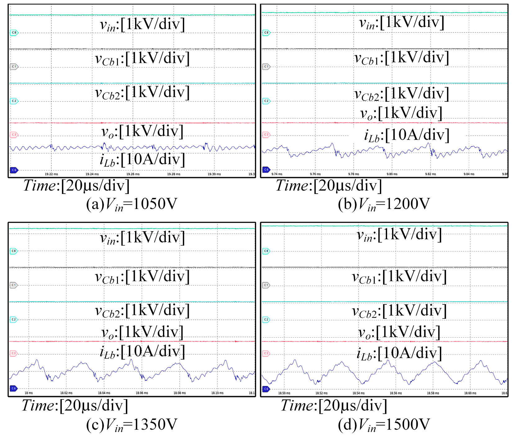
Figure 14 gives the experimental waveforms of the ISOP system under different input voltages. It can be seen that under different input voltages, the output voltages of the ISOP system are all stable at 700 V, and the intermediate bus voltages of the two groups of submodules show very good consistency.
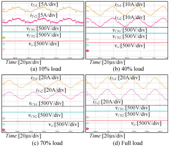
Figure 14.
Experimental waveforms at different loads.
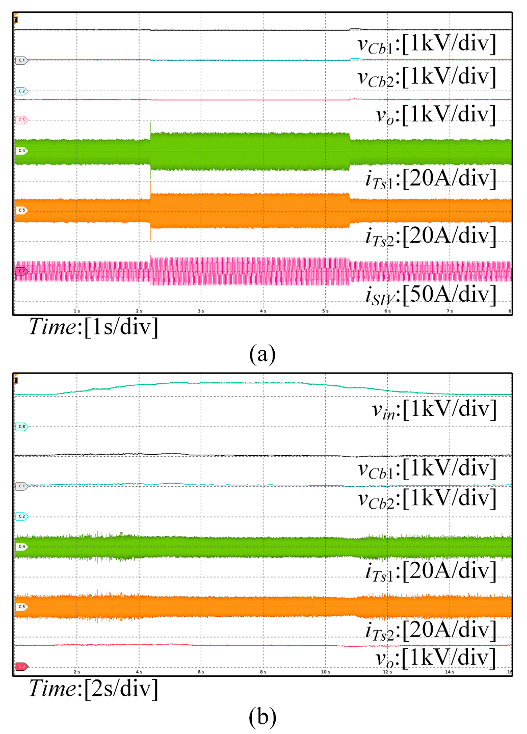
Figure 15a,b show the experimental waveforms of the converter when the load jumps and when the input voltage changes, respectively. It can be seen that the intermediate bus voltage and output current of the two groups of submodules show very good consistency without adopting an additional voltage and current equalization control strategy.
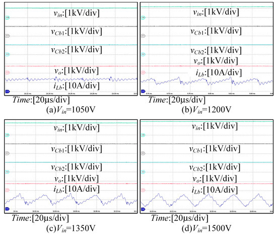
Figure 15.
Experimental waveforms at different input voltages.
Figure 16a,b shows that under the condition of different loads and different input voltages, even if the two sets of submodules of resonant inductance are inconsistent with excitation inductance parameters, the Boost + LLC cascaded module ISOP system still showed good pressure in the middle of the dc bus and output flow performance, verifying the validity of the theoretical analysis and simulation results.
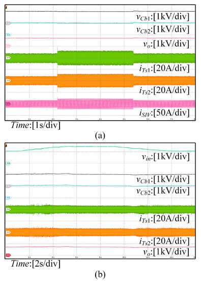
Figure 16.
Experimental waveforms when the load and input voltage change. (a) Experimental waveform of load jump; (b) experimental waveform of input voltage variation.
5. Conclusions
In this paper, we derive a second-order simplified small-signal model of the Boost + LLC topology based on the Boost + LLC modular input-series–output shunt converter system and study its input-voltage equalization and output-current equalization performance under the condition of inconsistent sub-module parameters. The analysis and experimental results show that the ISOP system has excellent self-leveling performance with the inconsistent parameters of the resonant inductance and excitation inductance of the two submodules and meets the performance index requirements of the full-bridge LLC resonant converter in open-loop conditions. It provides a theoretical basis for the optimal design of system parameters.
Author Contributions
Formal analysis, S.S.; Investigation, B.Z. and Y.S.; Methodology, J.H.; Resources, C.K.; Validation, Y.M.; Writing—original draft, X.L. and J.R.; Writing—review & editing, L.D. All authors have read and agreed to the published version of the manuscript.
Funding
This research was funded by Science and Technology Research and Development Plan of China National Railway Group Company Ltd. grants number L2021J001 and P2020J023.
Data Availability Statement
Not applicable.
Conflicts of Interest
The authors declare no conflict of interest.
References
- Luo, C.; Huang, S. Novel Voltage Balancing Control Strategy for Dual-Active-Bridge Input-Series-Output-Parallel DC-DC Converters. IEEE Access 2020, 8, 103114–103123. [Google Scholar] [CrossRef]
- Ma, D.; Chen, W.; Ruan, X. A Review of Voltage/Current Sharing Techniques for Series–Parallel-Connected Modular Power Conversion Systems. IEEE Trans. Power Electron. 2020, 35, 12383–12400. [Google Scholar] [CrossRef]
- Wang, Y.; Guan, Y.; Fosso, O.; Molinas, M.; Chen, S.-Z.; Zhang, Y. An Input-Voltage-Sharing Control Strategy of Input-Series-Output-Parallel Isolated Bidirectional DC/DC Converter for DC Distribution Network. IEEE Trans. Power Electron. 2021, 37, 1592–1604. [Google Scholar] [CrossRef]
- Sha, D.; Guo, Z.; Liao, X. Cross-Feedback Output-Current-Sharing Control for Input-Series-Output-Parallel Modular DC–DC Converters. IEEE Trans. Power Electron. 2010, 25, 2762–2771. [Google Scholar] [CrossRef]
- Duan, J.; Zhang, D.; Wang, L.; Zhou, Z.; Gu, Y. Active Voltage Sharing Module for Input-Series Connected Modular DC/DC Converters. IEEE Trans. Power Electron. 2020, 35, 5987–6000. [Google Scholar] [CrossRef]
- Ma, Q.; Huang, Q.; Huang, A.Q. Performance Analysis of an Input-Series-Output-Parallel LLC Resonant Converter with Parameters Mismatch. In Proceedings of the 2021 IEEE Energy Conversion Congress and Exposition (ECCE), Vancouver, BC, Canada, 10–14 October 2021; pp. 3203–3210. [Google Scholar]
- Liu, H.; Cui, S.; Liu, C.; Sun, H. Small-signal Modeling and Input Impedance of ISOP DC Transformer with Switched Resonant Branches for Self-Voltage Balancing. In Proceedings of the 2022 IEEE 5th International Electrical and Energy Conference (CIEEC), Nangjing, China, 27–29 May 2022; pp. 2818–2823. [Google Scholar]
- Fuerback, V.B.; Pagliosa, M.A.; Dall’Asta, M.S.; Lazzarin, T.B. Modular ISOP Flyback converter: Analysis of auto-balancing mechanism in steady state. In Proceedings of the 2017 IEEE 8th International Symposium on Power Electronics for Distributed Generation Systems (PEDG), Florianopolis, Brazil, 17–20 April 2017; pp. 1–6. [Google Scholar]
- Zong, S.; Zhu, Q.; Yu, W.; Huang, A.Q. Auxiliary power supply for solid state transformer with ultra high voltage capacitive driving. In Proceedings of the 2015 IEEE Applied Power Electronics Conference and Exposition (APEC), Charlotte, NC, USA, 15–19 March 2015; pp. 1008–1013. [Google Scholar]
- Shi, J.; Luo, J.; He, X. Common-Duty-Ratio Control of Input-Series Output-Parallel Connected Phase-shift Full-Bridge DC–DC Converter Modules. IEEE Trans. Power Electron. 2011, 26, 3318–3329. [Google Scholar] [CrossRef]
- Ding, R.; Mei, J.; Guan, Z.; Zhao, J. An Input-Series-Output-Series Modular Multilevel DC Transformer With Inter-Module Arithmetic Phase Interleaving Control to Reduce DC Ripples. IEEE Access 2018, 6, 75961–75974. [Google Scholar] [CrossRef]
- Wu, Y.-E.; Pan, B.-H. High Efficiency and Voltage Conversion Ratio Bidirectional Isolated DC-DC Converter for Energy Storage System. IEEE Access 2022, 10, 55187–55199. [Google Scholar] [CrossRef]
- Chang, C.; Cheng, C.; Cheng, H. Modeling and Design of the LLC Resonant Converter Used as a Solar-Array Simulator. IEEE J. Emerg. Sel. Topics Power Electron. 2014, 2, 833–841. [Google Scholar] [CrossRef]
- Tian, S.; Lee, F.C.; Li, Q. Equivalent Circuit Modeling of LLC Resonant Converter. IEEE Trans. Power Electron. 2020, 35, 8833–8845. [Google Scholar] [CrossRef]
- Liu, F.; Ruan, X.; Huang, X.; Qiu, Y. Second Harmonic Current Reduction for Two-Stage Inverter With DCX- LLC Resonant Converter in Front-End DC–DC Converter: Modeling and Control. IEEE Trans. Power Electron. 2021, 36, 4597–4609. [Google Scholar] [CrossRef]
- Hou, N.; Gunawardena, P.; Wu, X.; Ding, L.; Zhang, Y.; Li, Y.W. An Input-Oriented Power Sharing Control Scheme with Fast-Dynamic Response for ISOP DAB DC–DC Converter. IEEE Trans. Power Electron. 2022, 37, 6501–6510. [Google Scholar] [CrossRef]
- Zhang, Z.; Shi, Y.; Chen, Z.; Peng, K. ISOP DAB Application to the Test of Batteries. In Proceedings of the 2021 IEEE 4th International Conference on Renewable Energy and Power Engineering (REPE), Beijing, China, 9–11 October 2021; pp. 43–47. [Google Scholar]

Publisher’s Note: MDPI stays neutral with regard to jurisdictional claims in published maps and institutional affiliations. |
© 2022 by the authors. Licensee MDPI, Basel, Switzerland. This article is an open access article distributed under the terms and conditions of the Creative Commons Attribution (CC BY) license (https://creativecommons.org/licenses/by/4.0/).