
Non-Isolated Interleaved Hybrid Boost Converter for Renewable Energy Applications


Abstract
:1. Introduction
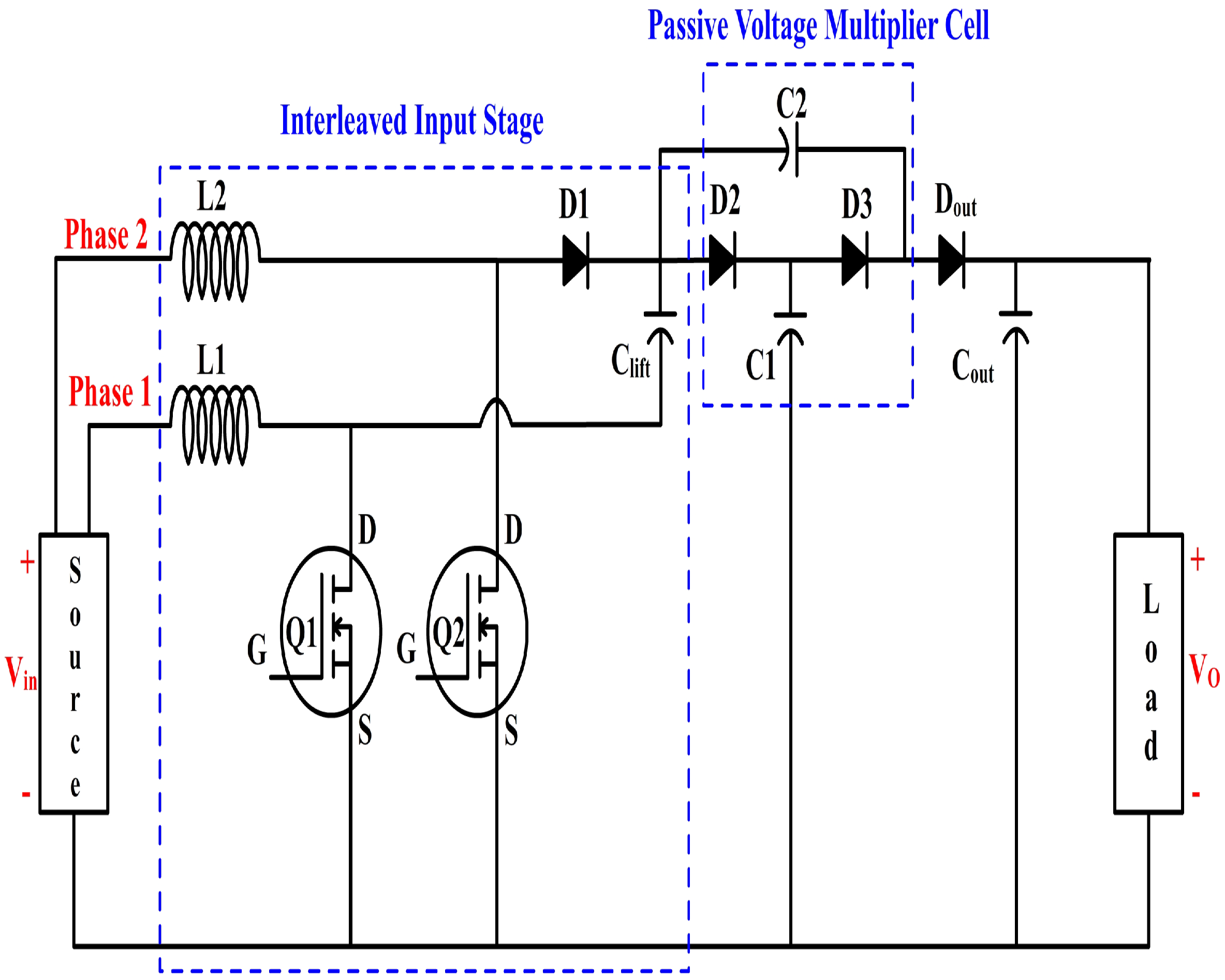
1.1. Proposed Converter
1.2. Modes of Operation
1.2.1. Group 1: Duty > 50%
1.2.2. Group 2: Duty < 50%
2. Analysis
2.1. Analysis of Group 1 Operation
2.2. Analysis of Group 2 Operation
3. Converter Design
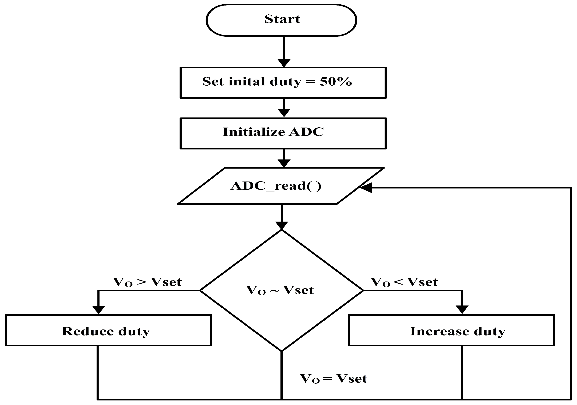
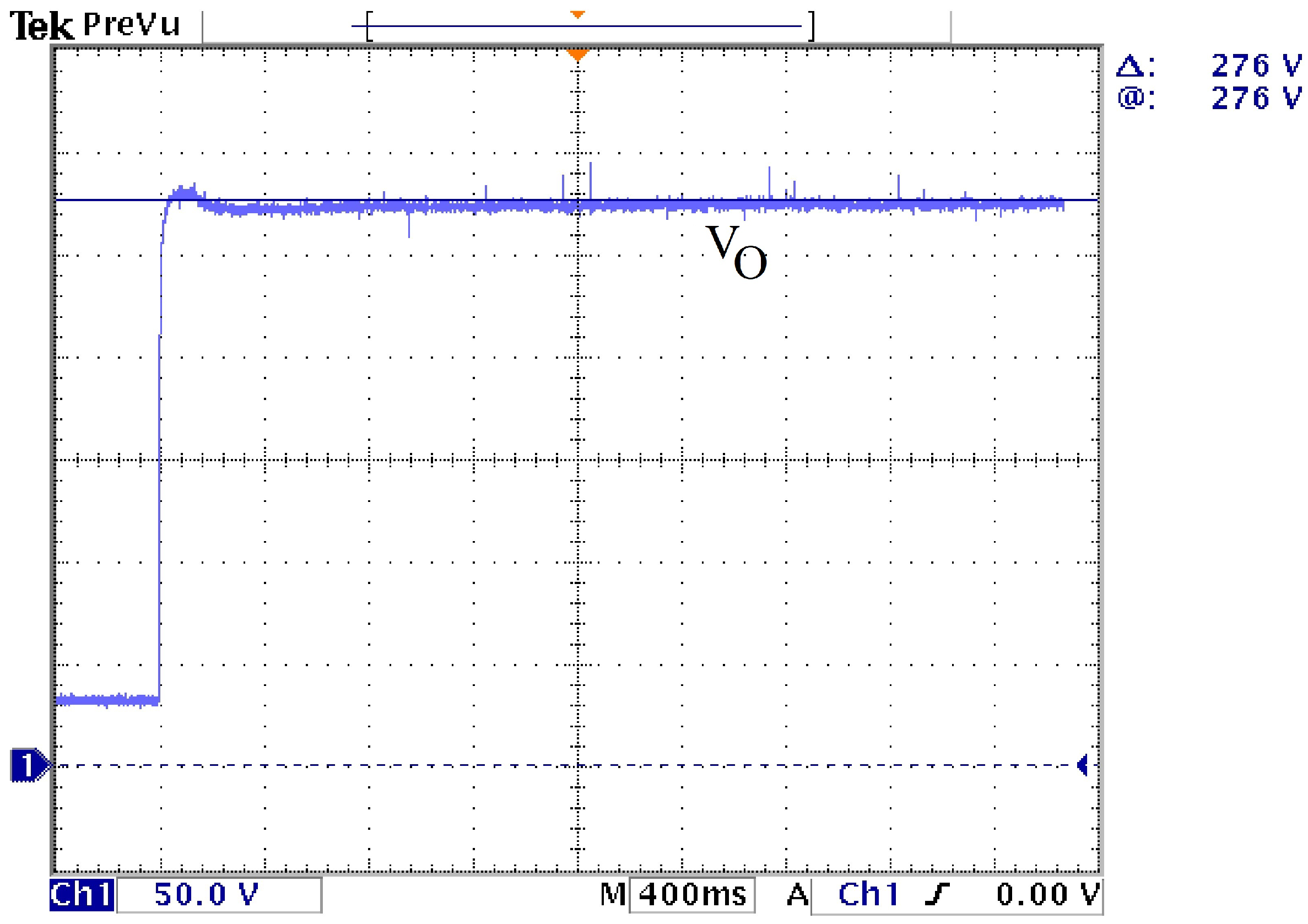
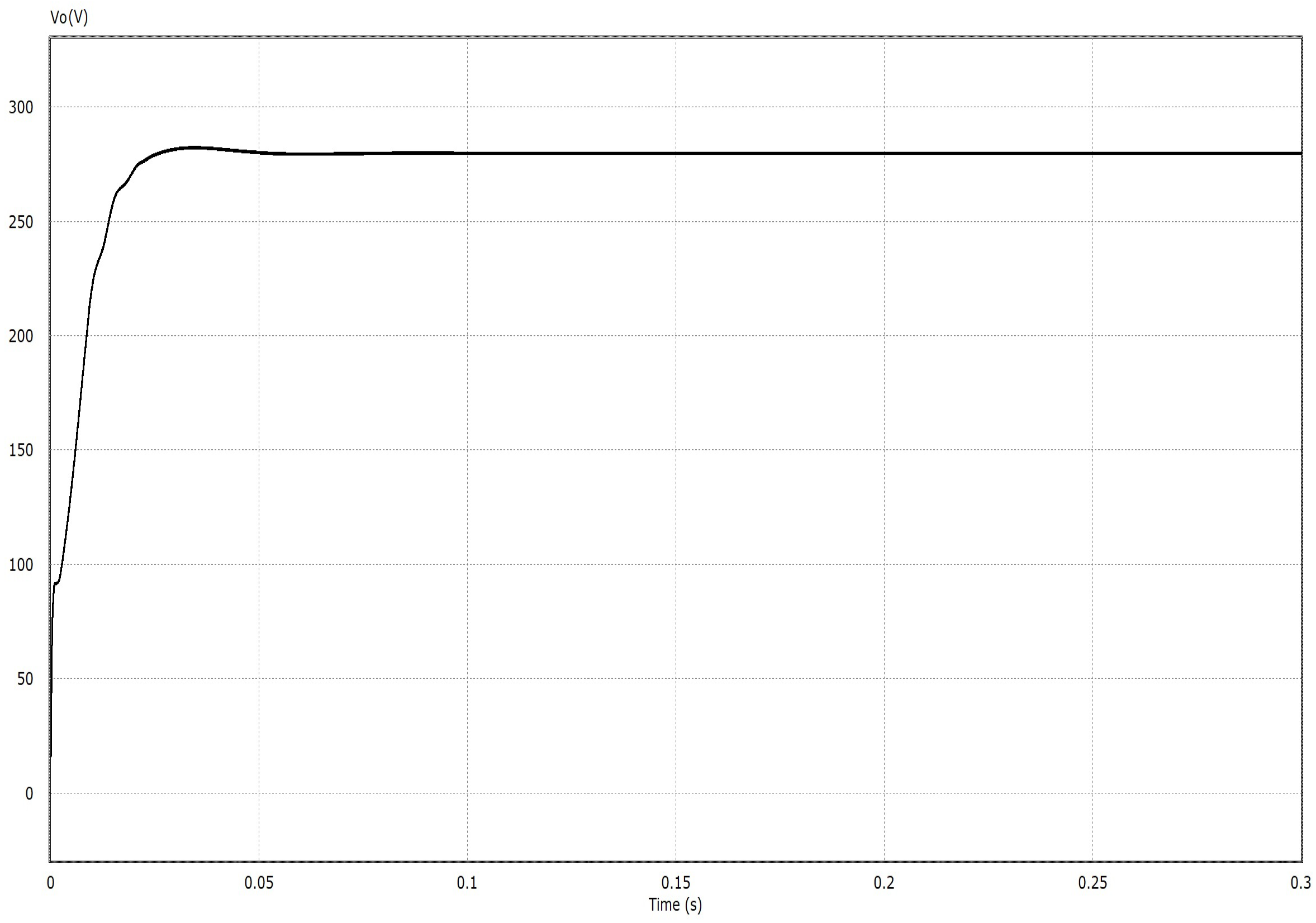
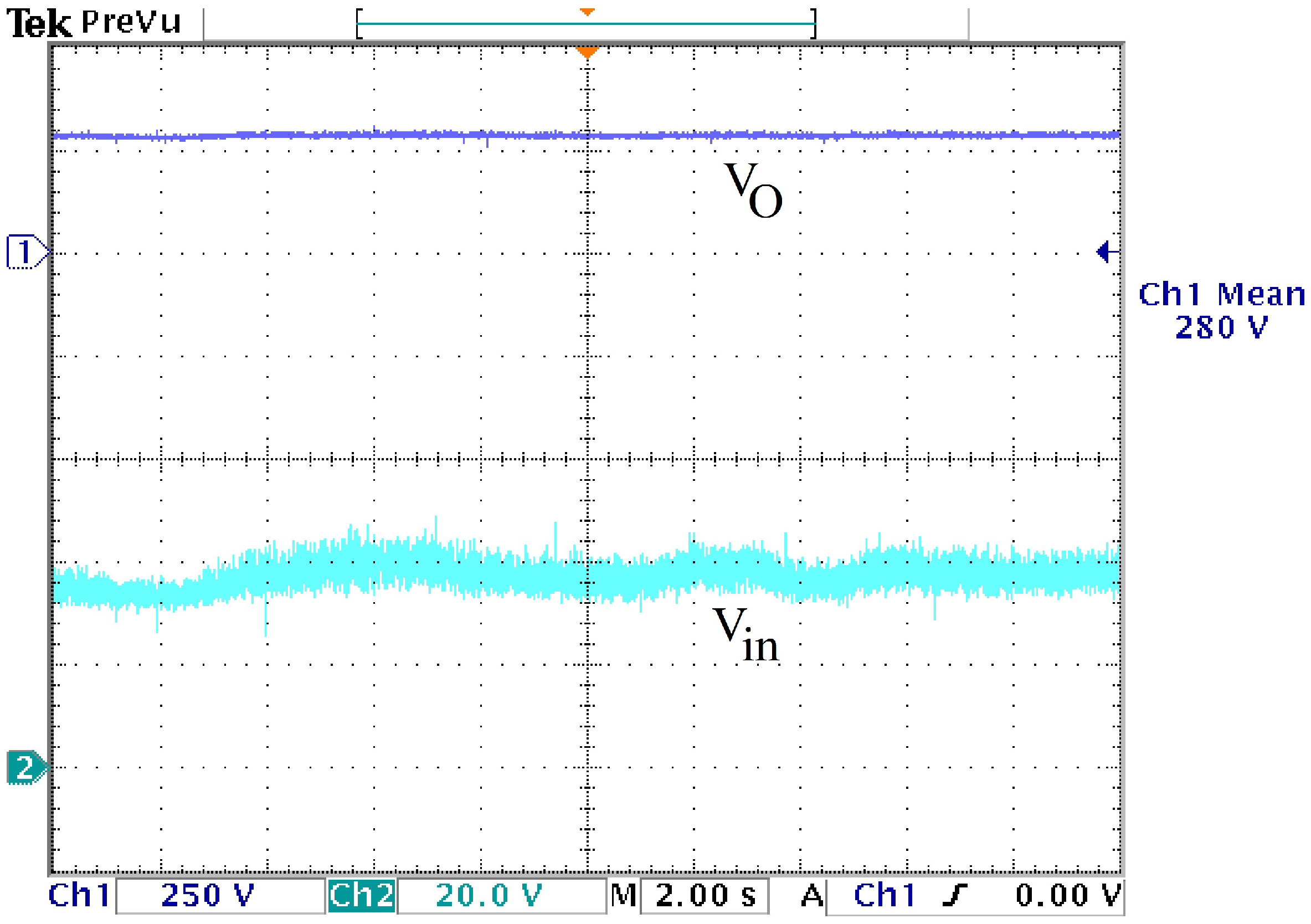
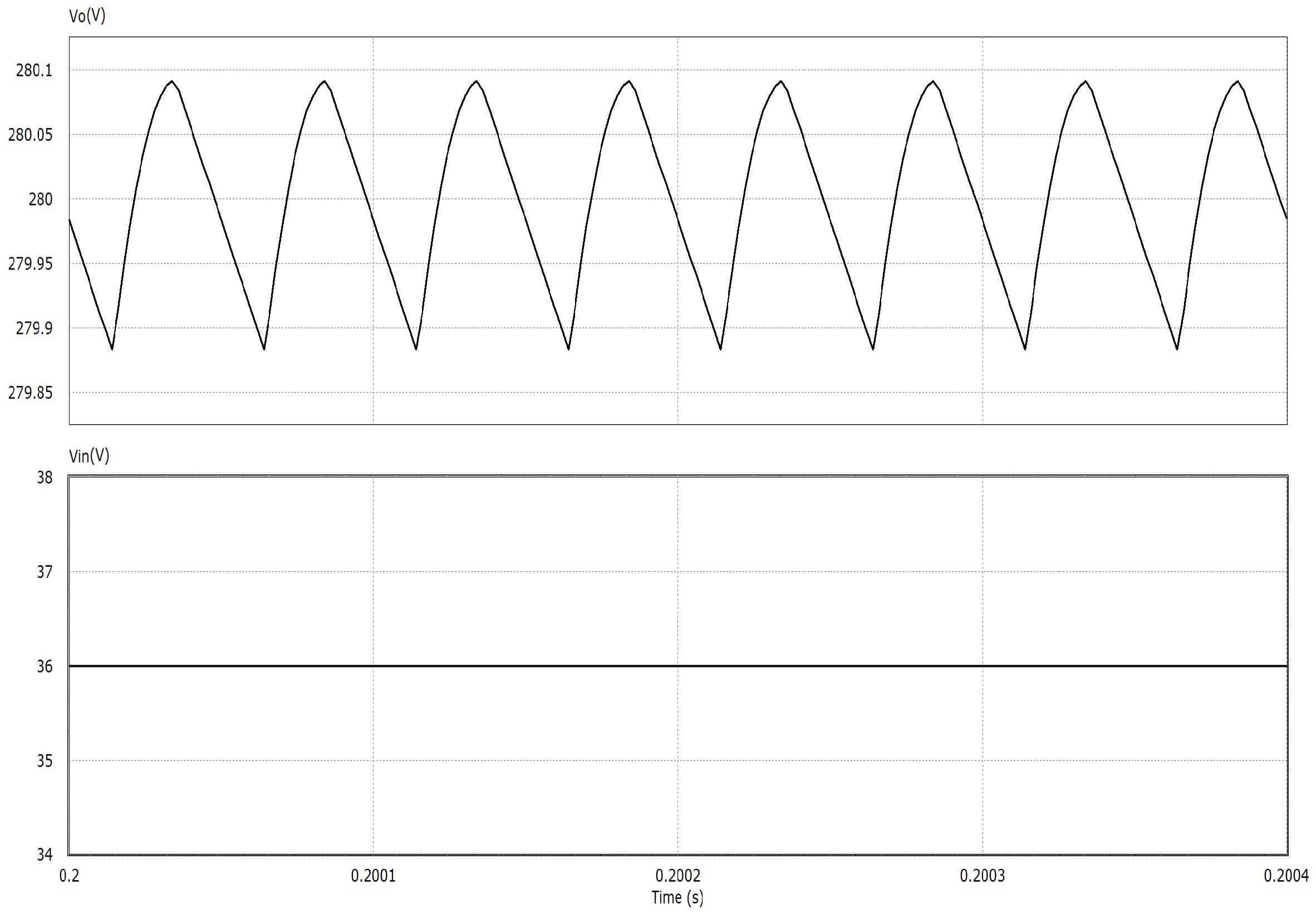
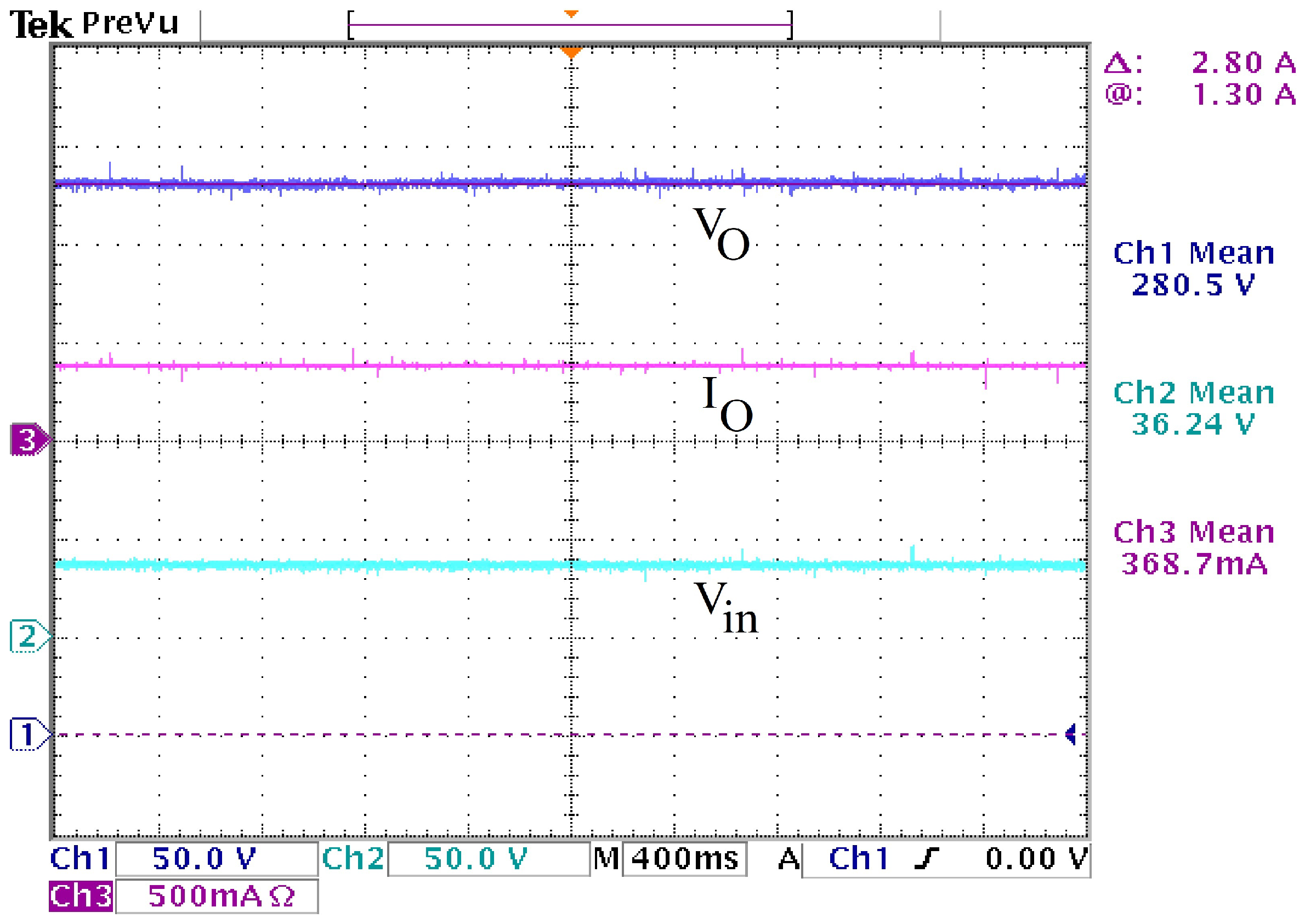
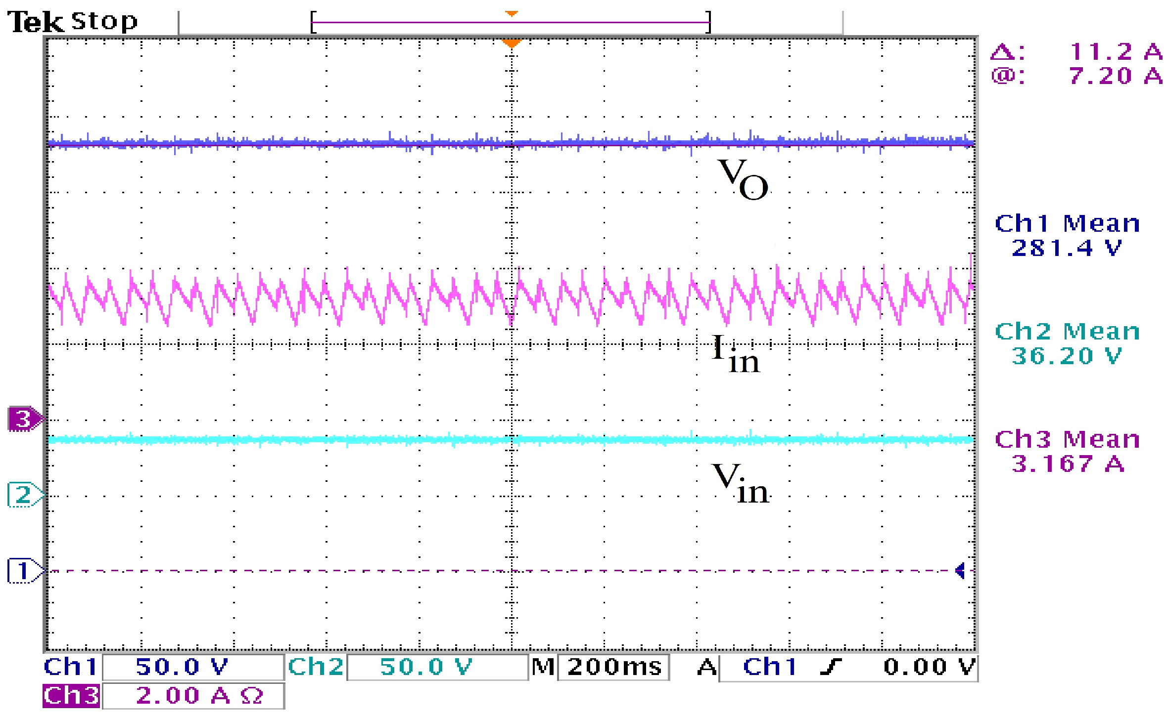
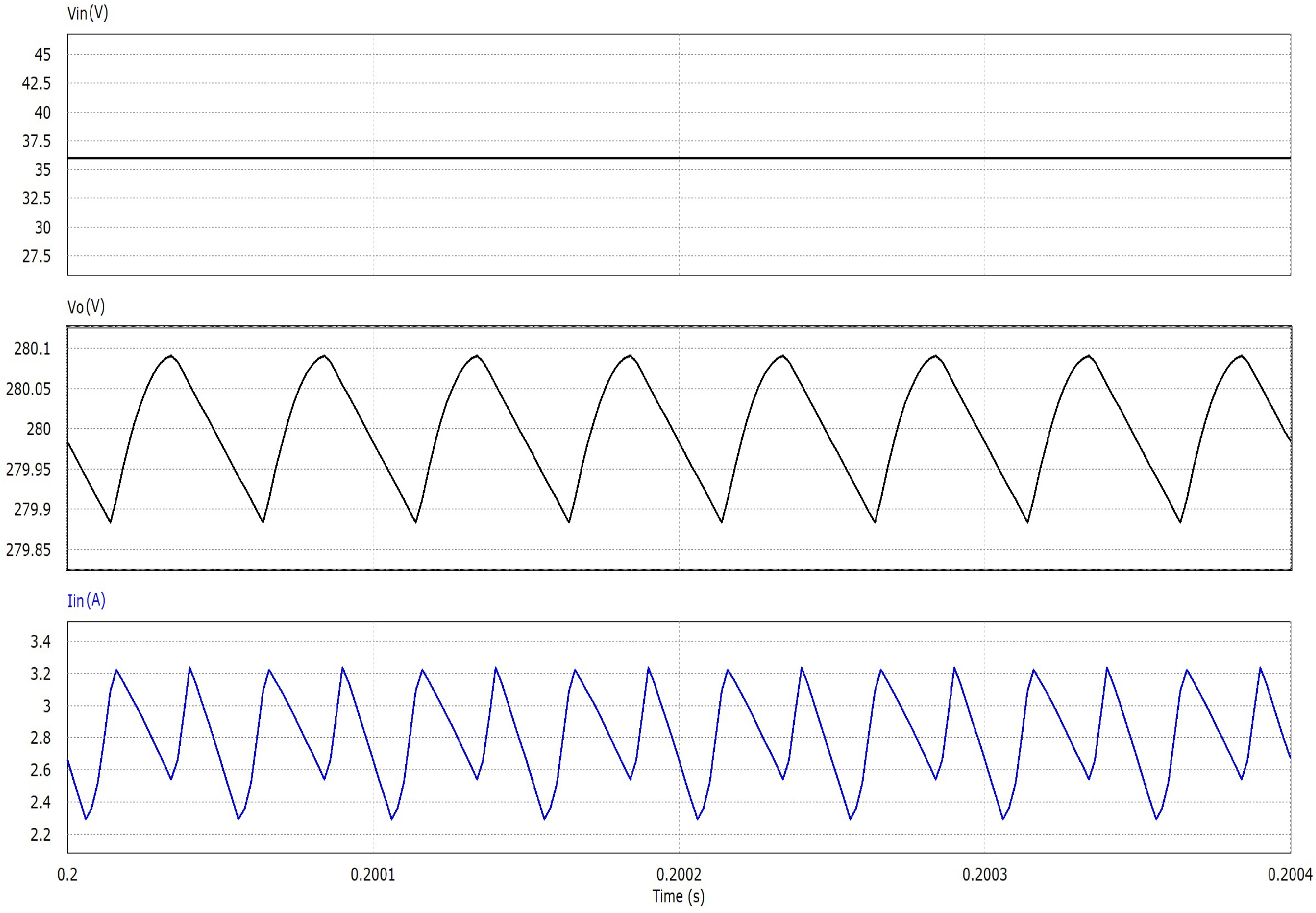
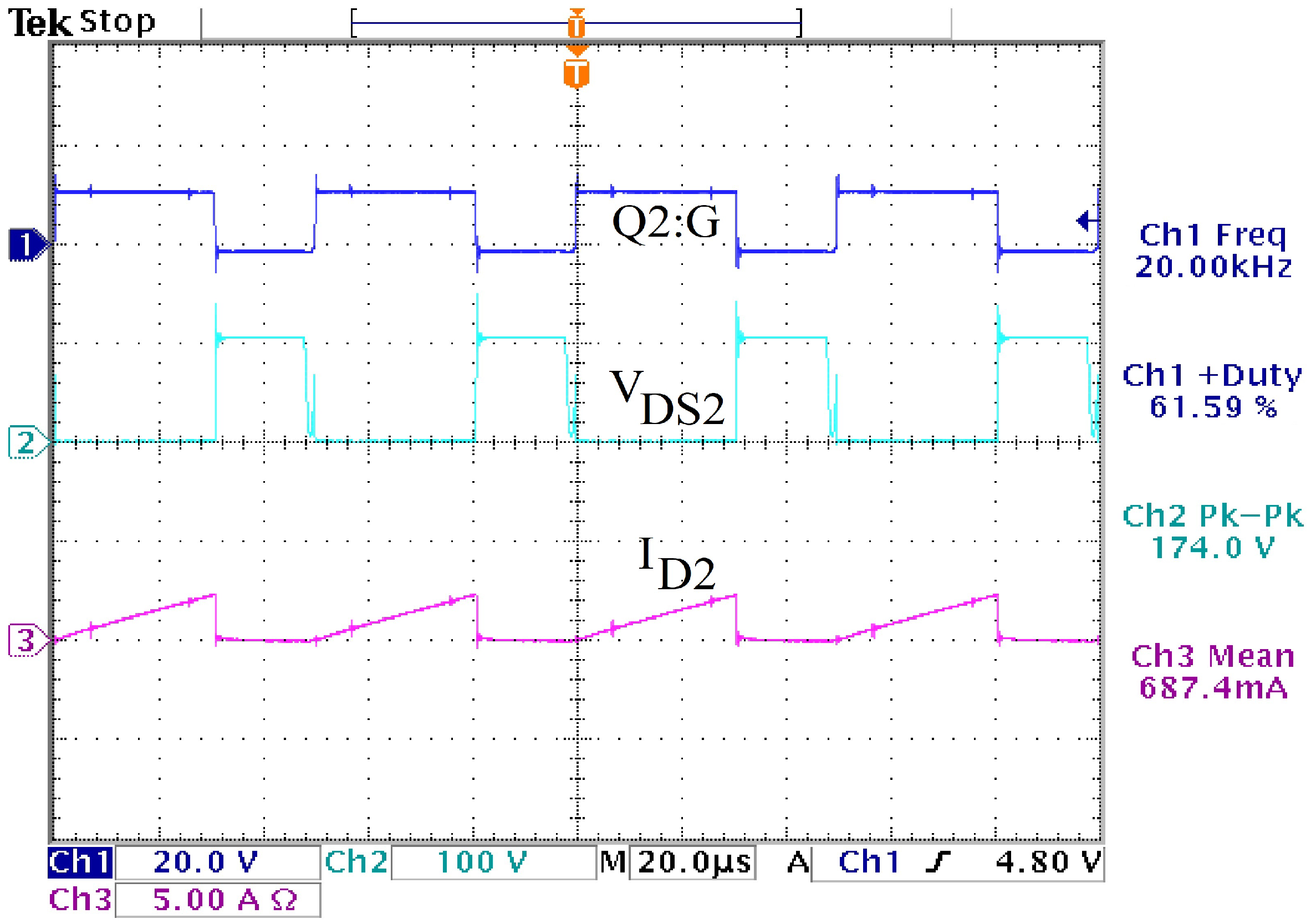
4. Results
5. Conclusions
Author Contributions
Funding
Institutional Review Board Statement
Informed Consent Statement
Data Availability Statement
Conflicts of Interest
References
- Luo, F.; Zhang, T.; Mi, Z.; Li, F.; Bai, L.; Liu, G.; Sun, Q.; Wang, X. Study on low-carbon comprehensive benefits of grid-connected photovoltaic generation. In Proceedings of the 2015 IEEE Power & Energy Society General Meeting, Denver, CO, USA, 26–30 July 2015; pp. 1–5. [Google Scholar]
- Köberle, A.C.; Gernaat, D.E.; van Vuuren, D.P. Assessing current and future techno-economic potential of concentrated solar power and photovoltaic electricity generation. Energy 2015, 89, 739–756. [Google Scholar] [CrossRef] [Green Version]
- Silvestre, S.; Chouder, A. Effects of shadowing on photovoltaic module performance. Prog. Photovolt. Res. Appl. 2008, 16, 141–149. [Google Scholar] [CrossRef]
- Sullivan, C.R.; Awerbuch, J.J.; Latham, A.M. Decrease in photovoltaic power output from ripple: Simple general calculation and the effect of partial shading. IEEE Trans. Power Electron. 2012, 28, 740–747. [Google Scholar] [CrossRef]
- Das, M.; Agarwal, V. Novel High-Performance Stand-Alone Solar PV System With High-Gain High-Efficiency DC–DC Converter Power Stages. IEEE Trans. Ind. Appl. 2015, 51, 4718–4728. [Google Scholar] [CrossRef]
- Debnath, D.; Chatterjee, K. Two-Stage Solar Photovoltaic-Based Stand-Alone Scheme Having Battery as Energy Storage Element for Rural Deployment. IEEE Trans. Ind. Electron. 2015, 62, 4148–4157. [Google Scholar] [CrossRef]
- Eltamaly, A.M. Performance of smart maximum power point tracker under partial shading conditions of photovoltaic systems. J. Renew. Sustain. Energy 2015, 7, 043141. [Google Scholar] [CrossRef]
- Erickson, R.W.; Maksimovic, D. Fundamentals of Power Electronics; Springer Science & Business Media: Berlin/Heidelberg, Germany, 2007. [Google Scholar]
- Maksimovic, D.; Cuk, S. Switching converters with wide DC conversion range. IEEE Trans. Power Electron. 1991, 6, 151–157. [Google Scholar] [CrossRef]
- Sreekanth, T.; Lakshminarasamma, N.; Mishra, M.K. A single-stage grid-connected high gain buck–boost inverter with maximum power point tracking. IEEE Trans. Energy Convers. 2016, 32, 330–339. [Google Scholar] [CrossRef]
- Wu, T.F.; Chen, Y.C.; Yang, J.G.; Huang, Y.C.; Shyu, S.S.; Lee, C.L. 1.5 kW isolated bi-directional DC-DC converter with a flyback snubber. In Proceedings of the 2009 International Conference on Power Electronics and Drive Systems (PEDS), Taipei, Taiwan, 2–5 November 2009; pp. 164–169. [Google Scholar] [CrossRef] [Green Version]
- Hu, H.; Harb, S.; Fang, X.; Zhang, D.; Zhang, Q.; Shen, Z.J.; Batarseh, I. A Three-port Flyback for PV Microinverter Applications With Power Pulsation Decoupling Capability. IEEE Trans. Power Electron. 2012, 27, 3953–3964. [Google Scholar] [CrossRef]
- Wu, H.; Mu, T.; Ge, H.; Xing, Y. Full-Range Soft-Switching-Isolated Buck-Boost Converters with Integrated Interleaved Boost Converter and Phase-Shifted Control. IEEE Trans. Power Electron. 2016, 31, 987–999. [Google Scholar] [CrossRef]
- Axelrod, B.; Berkovich, Y.; Ioinovici, A. Transformerless DC-DC converters with a very high DC line-to-load voltage ratio. In Proceedings of the 2003 International Symposium on Circuits and Systems, ISCAS’03, Bangkok, Thailand, 25–28 May 2003; Volume 3, p. III. [Google Scholar]
- Poorali, B.; Moradmand Jazi, H.; Adib, E. Single-core soft-switching high step-up three-level boost converter with active clamp. IET Power Electron. 2016, 9, 2692–2699. [Google Scholar] [CrossRef]
- Ye, Y.; Cheng, K.W.E.; Chen, S. A High Step-up PWM DC-DC Converter with Coupled-Inductor and Resonant Switched-Capacitor. IEEE Trans. Power Electron. 2017, 32, 7739–7749. [Google Scholar] [CrossRef]
- Siwakoti, Y.P.; Blaabjerg, F. Single Switch Nonisolated Ultra-Step-Up DC–DC Converter with an Integrated Coupled Inductor for High Boost Applications. IEEE Trans. Power Electron. 2017, 32, 8544–8558. [Google Scholar] [CrossRef]
- Vecchia, M.D.; Salvador, M.A.; Lazzarin, T.B. Hybrid Nonisolated DC–DC Converters Derived From a Passive Switched-Capacitor Cell. IEEE Trans. Power Electron. 2018, 33, 3157–3168. [Google Scholar] [CrossRef]
- Hu, X.; Wang, J.; Li, L.; Li, Y. A Three-Winding Coupled-Inductor DC–DC Converter Topology with High Voltage Gain and Reduced Switch Stress. IEEE Trans. Power Electron. 2018, 33, 1453–1462. [Google Scholar] [CrossRef]
- Jahangiri, H.; Mohammadpour, S.; Ajami, A. A high step-up DC-DC boost converter with coupled inductor based on quadratic converters. In Proceedings of the 2018 9th Annual Power Electronics, Drives Systems and Technologies Conference (PEDSTC), Tehran, Iran, 13–15 February 2018; pp. 20–25. [Google Scholar] [CrossRef]
- Andrade, A.M.S.S.; Mattos, E.; Schuch, L.; Hey, H.L.; da Silva Martins, M.L. Synthesis and Comparative Analysis of Very High Step-Up DC–DC Converters Adopting Coupled-Inductor and Voltage Multiplier Cells. IEEE Trans. Power Electron. 2018, 33, 5880–5897. [Google Scholar] [CrossRef]
- Mahmoudi, M.; Ajami, A.; Babaei, E.; Abdolmaleki, N.; Wang, C. A High Gain DC-DC Topology Based on Two-Winding Coupled Inductors Featuring Continuous Input Current. In Proceedings of the 2020 IEEE Energy Conversion Congress and Exposition (ECCE), Detroit, MI, USA, 11–15 October 2020; pp. 4782–4787. [Google Scholar] [CrossRef]
- Prudente, M.; Pfitscher, L.L.; Emmendoerfer, G.; Romaneli, E.F.; Gules, R. Voltage Multiplier Cells Applied to Non-Isolated DC–DC Converters. IEEE Trans. Power Electron. 2008, 23, 871–887. [Google Scholar] [CrossRef]
- Girish Ganesan, R.; Prabhakar, M. Multi-level dc-dc converter for high gain applications. Int. J. Power Electron. Drive Syst. 2013, 3, 365–373. [Google Scholar]
- Girish Ganesan, R.; Prabhakar, M. Non-isolated high step-up interleaved boost converter. Int. J. Power Electron. 2014, 6, 288–303. [Google Scholar] [CrossRef]
- An, L.; Lu, D.D.C. Analysis of DC Bus Capacitor Current Ripple Reduction in Basic DC/DC Cascaded Two-Stage Power Converters. IEEE Trans. Ind. Electron. 2016, 63, 7467–7477. [Google Scholar] [CrossRef]
- Yang, J.; Yu, D.; Cheng, H.; Zan, X.; Wen, H. Dual-coupled inductors-based high step-up DC/DC converter without input electrolytic capacitor for PV application. IET Power Electron. 2017, 10, 646–656. [Google Scholar] [CrossRef]
- Porselvi, T.; Arounassalame, M. A novel Single Switch High Gain dc-dc Converter. In Proceedings of the 2018 8th IEEE India International Conference on Power Electronics (IICPE), Jaipur, India, 13–15 December 2018; pp. 1–6. [Google Scholar] [CrossRef]
- Liccardo, F.; Marino, P.; Torre, G.; Triggianese, M. Interleaved dc-dc Converters for Photovoltaic Modules. In Proceedings of the 2007 International Conference on Clean Electrical Power, Capri, Italy, 21–23 May 2007; pp. 201–207. [Google Scholar] [CrossRef]
- Ramabadran, R.; Balaji, K.; Raj, S.; Logeshwaran, V. Comparison of Interleaved Boost Converter Configurations for Solar Photovoltaic System Interface. J. Eng. Res. 2013, 10, 87–98. [Google Scholar] [CrossRef] [Green Version]
- Prasanth, P.; Ramalingam, S. Investigation of Four Phase Interleaved Boost Converter under Open Loop and Closed Loop Control Schemes for Battery Charging Applications. Int. J. Adv. Mater. Sci. Eng. 2016, 5, 11–20. [Google Scholar] [CrossRef]
- Kumar, C.P.; Mahesh, M. Development of interleaved boost dc-dc converter with closed loop control. In Proceedings of the 2016 IEEE Annual India Conference (INDICON), Bangalore, India, 16–18 December 2016; pp. 1–5. [Google Scholar] [CrossRef]
- Farh, H.M.H.; Othman, M.F.; Eltamaly, A.M.; Al-Saud, M.S. Maximum Power Extraction from a Partially Shaded PV System Using an Interleaved Boost Converter. Energies 2018, 11, 2543. [Google Scholar] [CrossRef] [Green Version]
- Farh, H.M.; Eltamaly, A.M.; Al-Saud, M.S. Interleaved boost converter for global maximum power extraction from the photovoltaic system under partial shading. IET Renew. Power Gener. 2019, 13, 1232–1238. [Google Scholar] [CrossRef]
- Lee, P.W.; Lee, Y.S.; Cheng, D.; Liu, X.C. Steady-state analysis of an interleaved boost converter with coupled inductors. IEEE Trans. Ind. Electron. 2000, 47, 787–795. [Google Scholar] [CrossRef]
- Arango, E.; Ramos-Paja, C.A.; Calvente, J.; Giral, R.; Serna, S. Asymmetrical Interleaved DC/DC Switching Converters for Photovoltaic and Fuel Cell Applications—Part 1: Circuit Generation, Analysis and Design. Energies 2012, 5, 4590–4623. [Google Scholar] [CrossRef] [Green Version]
- Muhammad, M.; Armstrong, M.; Elgendy, M.A. A Nonisolated Interleaved Boost Converter for High-Voltage Gain Applications. IEEE J. Emerg. Sel. Top. Power Electron. 2016, 4, 352–362. [Google Scholar] [CrossRef] [Green Version]


| Parameter | Value/Description |
|---|---|
| 500 H | |
| 500 H | |
| 10 F/100 V | |
| 10 F/100 V | |
| 10 F/200 V | |
| 68 F/350 V | |
| Switches and | FDP2552 |
| Diodes | STTH302 |
| Voltage Sensor | LV25-P |
| Controller | Microchip PIC16F18455 |
| MOSFET Drivers | TLP250 |
| Switching Frequency | 20 kHz |
Publisher’s Note: MDPI stays neutral with regard to jurisdictional claims in published maps and institutional affiliations. |
© 2022 by the authors. Licensee MDPI, Basel, Switzerland. This article is an open access article distributed under the terms and conditions of the Creative Commons Attribution (CC BY) license (https://creativecommons.org/licenses/by/4.0/).
Share and Cite
Ramanathan, G.G.; Urasaki, N. Non-Isolated Interleaved Hybrid Boost Converter for Renewable Energy Applications. Energies 2022, 15, 610. https://doi.org/10.3390/en15020610
Ramanathan GG, Urasaki N. Non-Isolated Interleaved Hybrid Boost Converter for Renewable Energy Applications. Energies. 2022; 15(2):610. https://doi.org/10.3390/en15020610
Chicago/Turabian StyleRamanathan, Girish Ganesan, and Naomitsu Urasaki. 2022. "Non-Isolated Interleaved Hybrid Boost Converter for Renewable Energy Applications" Energies 15, no. 2: 610. https://doi.org/10.3390/en15020610
APA StyleRamanathan, G. G., & Urasaki, N. (2022). Non-Isolated Interleaved Hybrid Boost Converter for Renewable Energy Applications. Energies, 15(2), 610. https://doi.org/10.3390/en15020610