
Unipolar Arc Ignited Partial Discharge for 650-V AlGaN/GaN HEMTs during the DC Breakdown Voltage Measurement
 ,
, 
Abstract
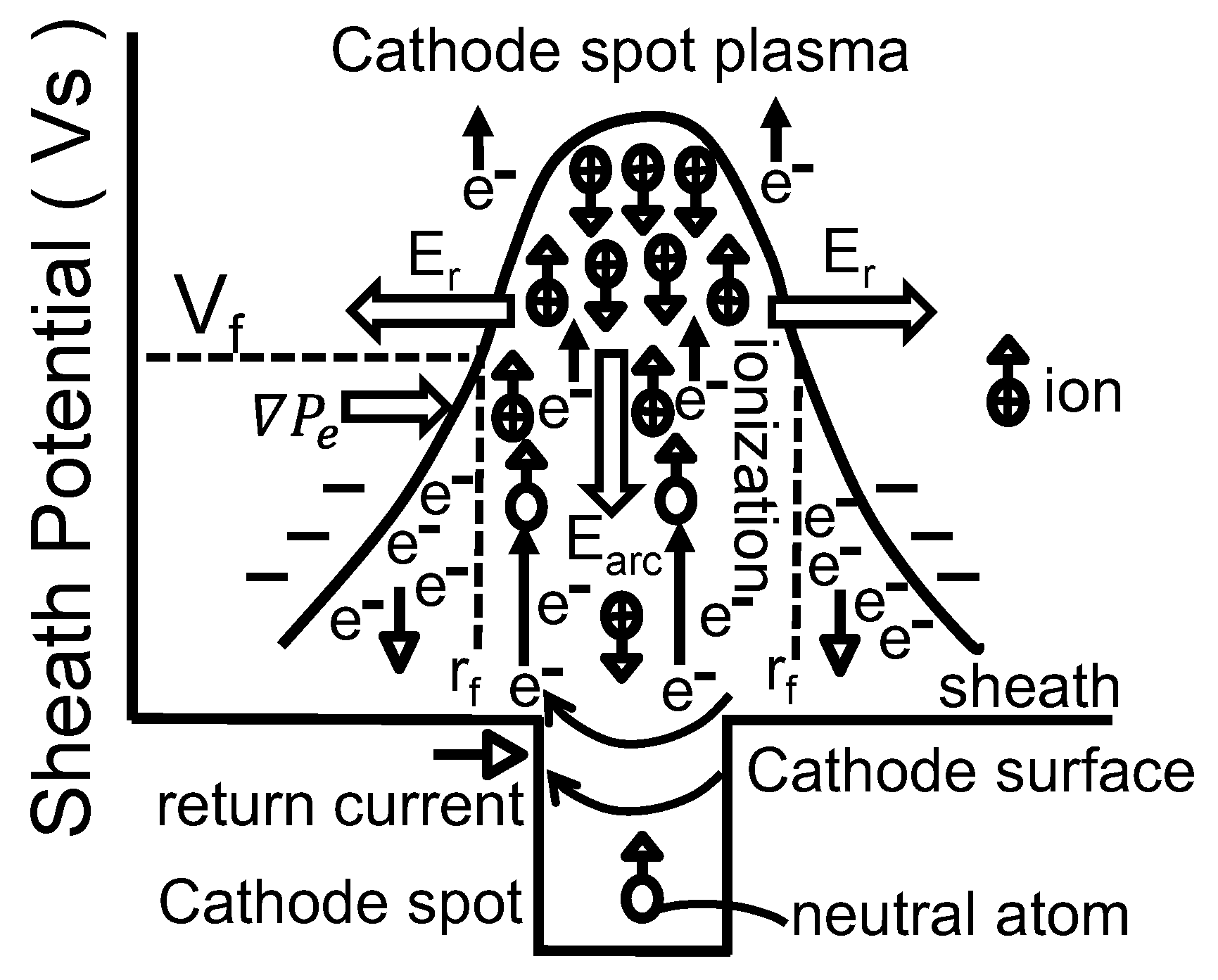
:1. Introduction
- the voltage should be higher than the avalanche breakdown voltage.
- Electrons must exist for impact–ionization generation.
- The electric field should be larger than the critical field.
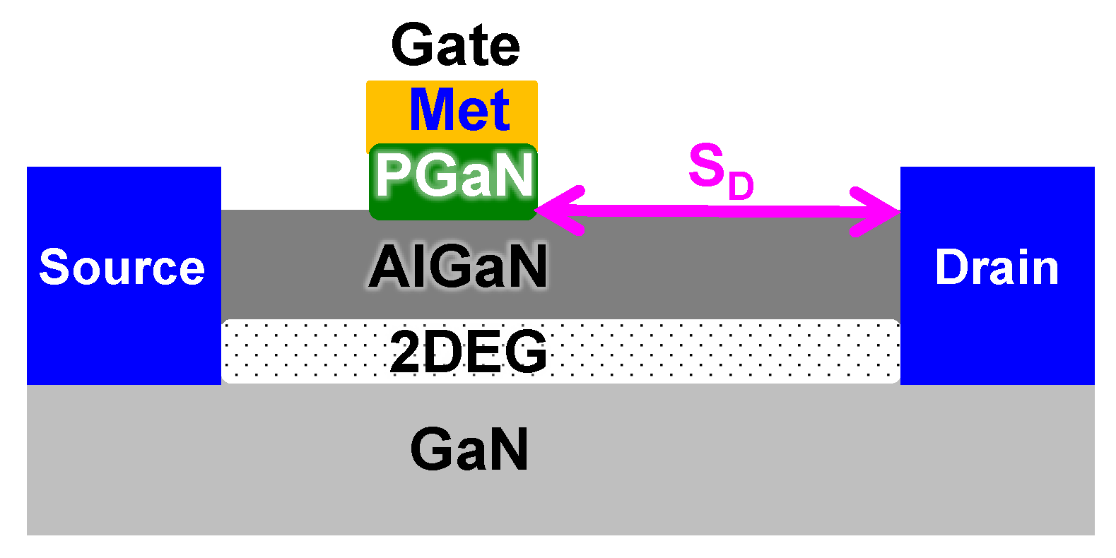
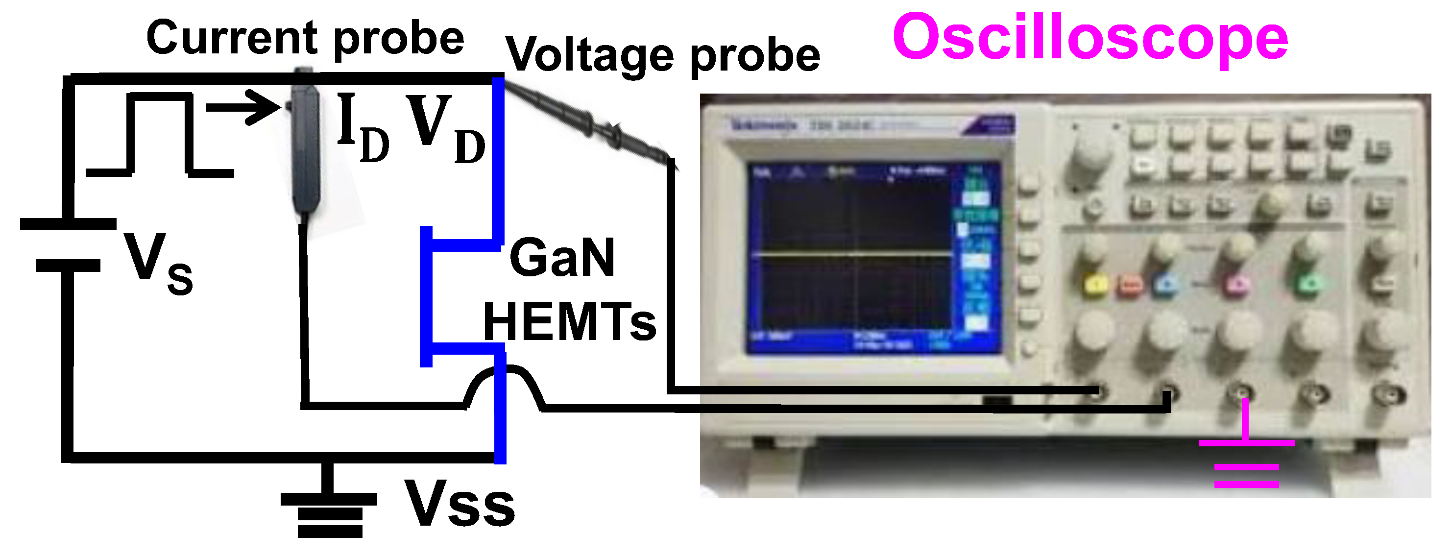
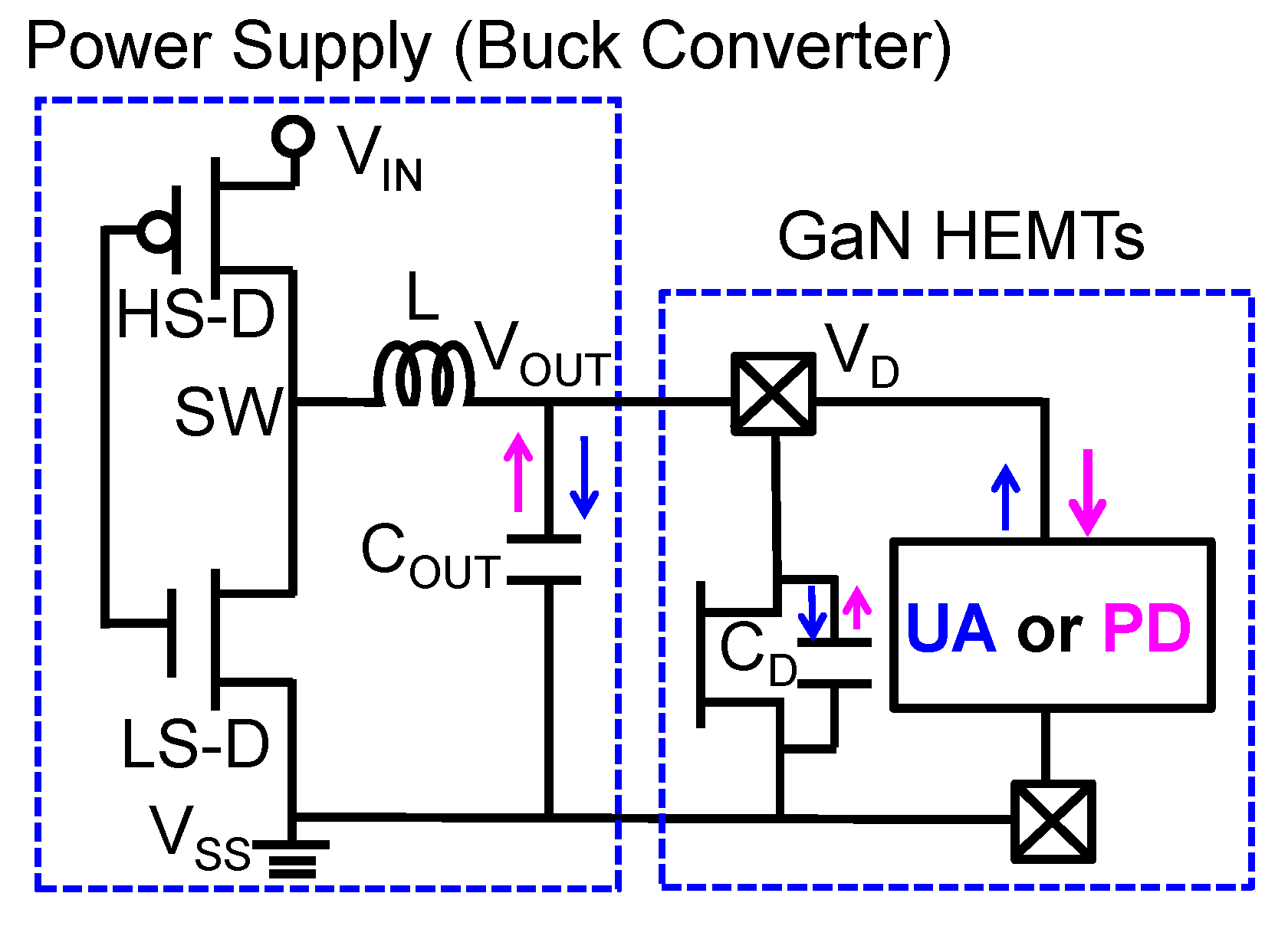
2. Experiment
3. Results
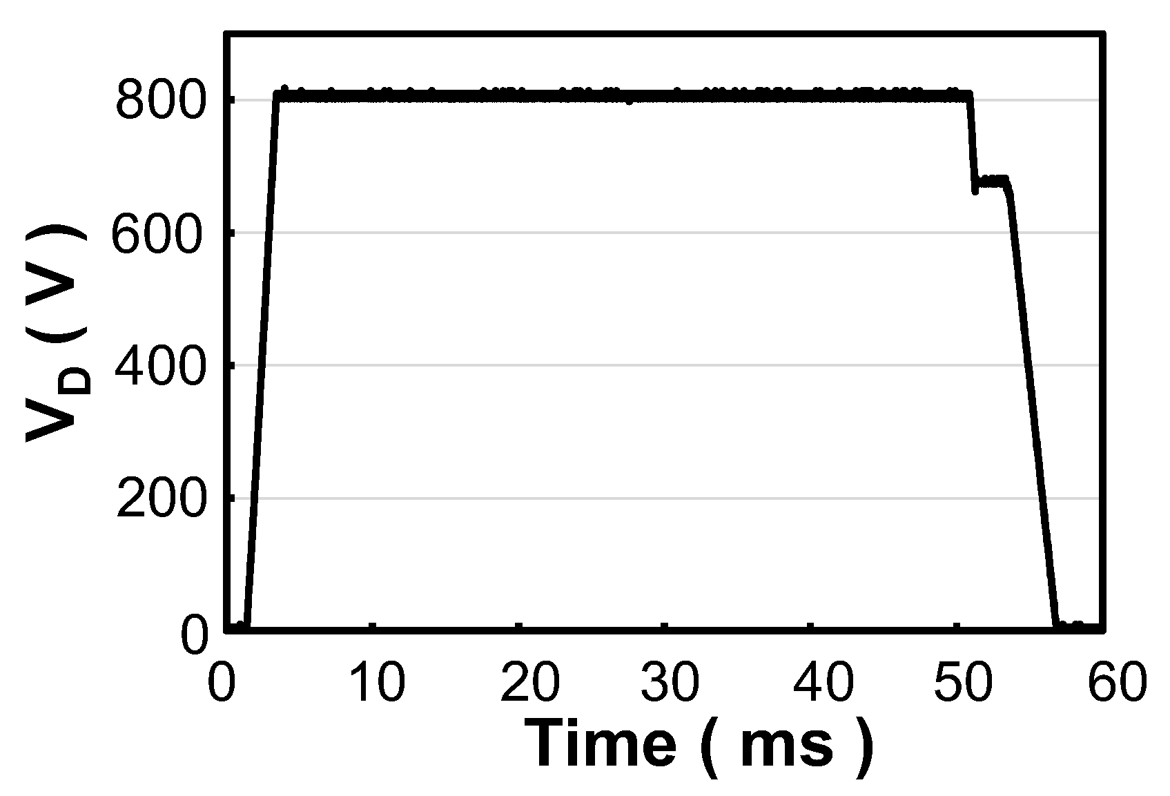
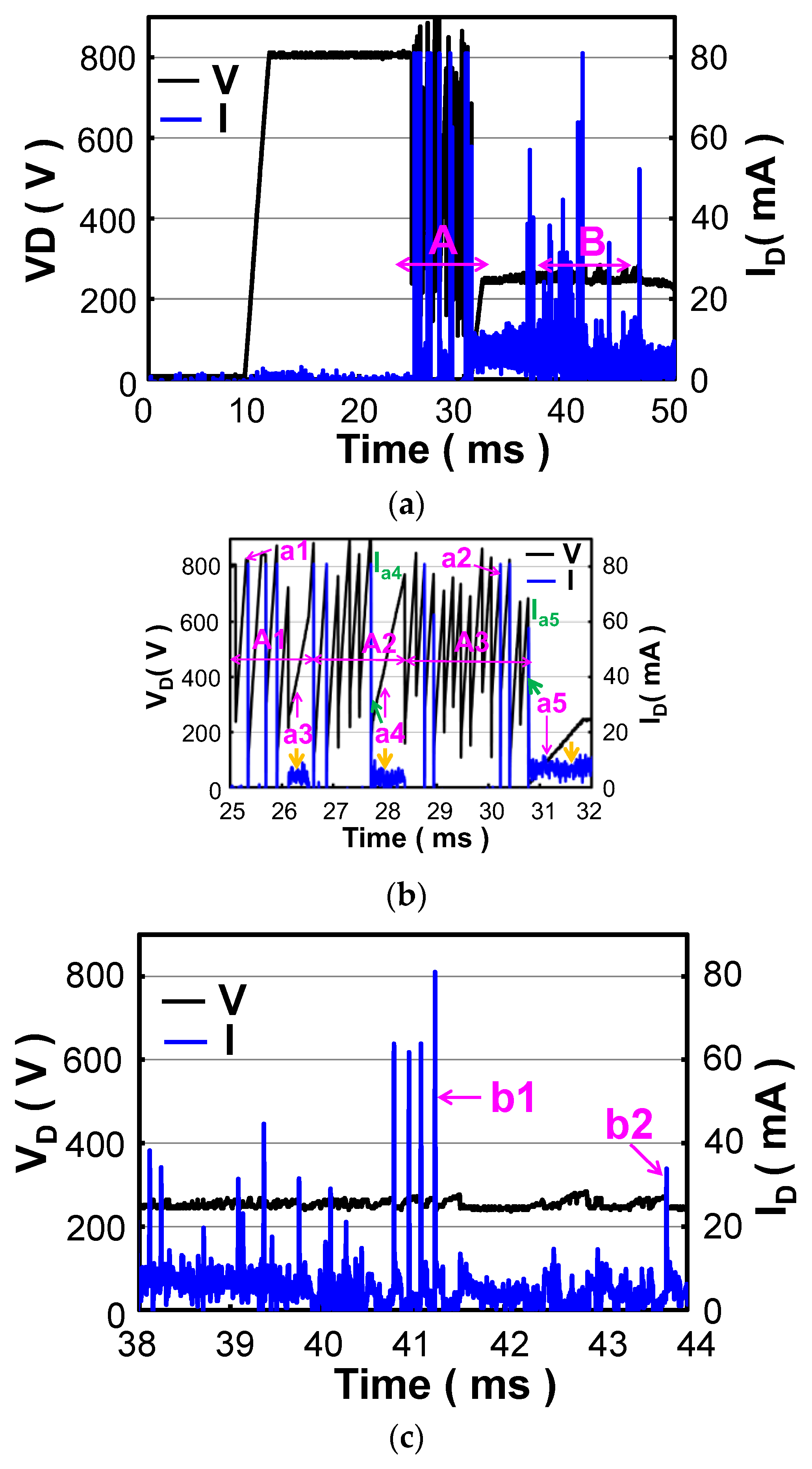
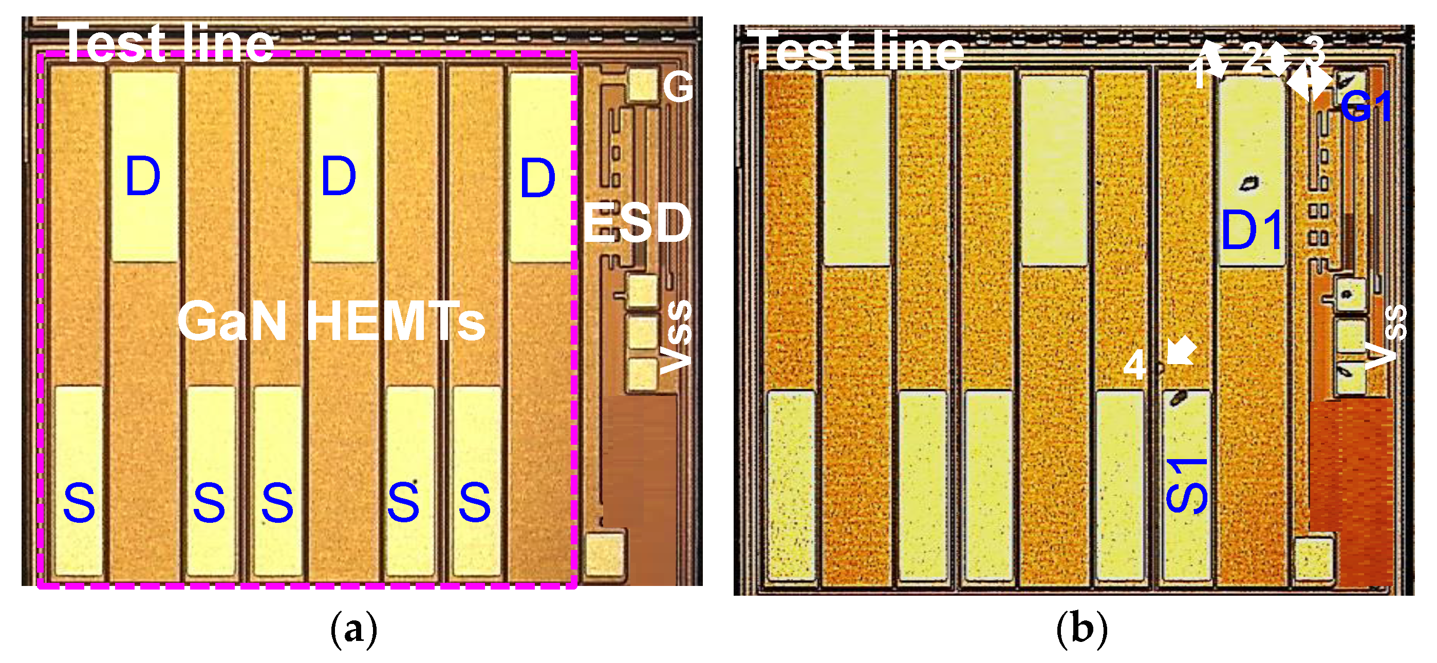
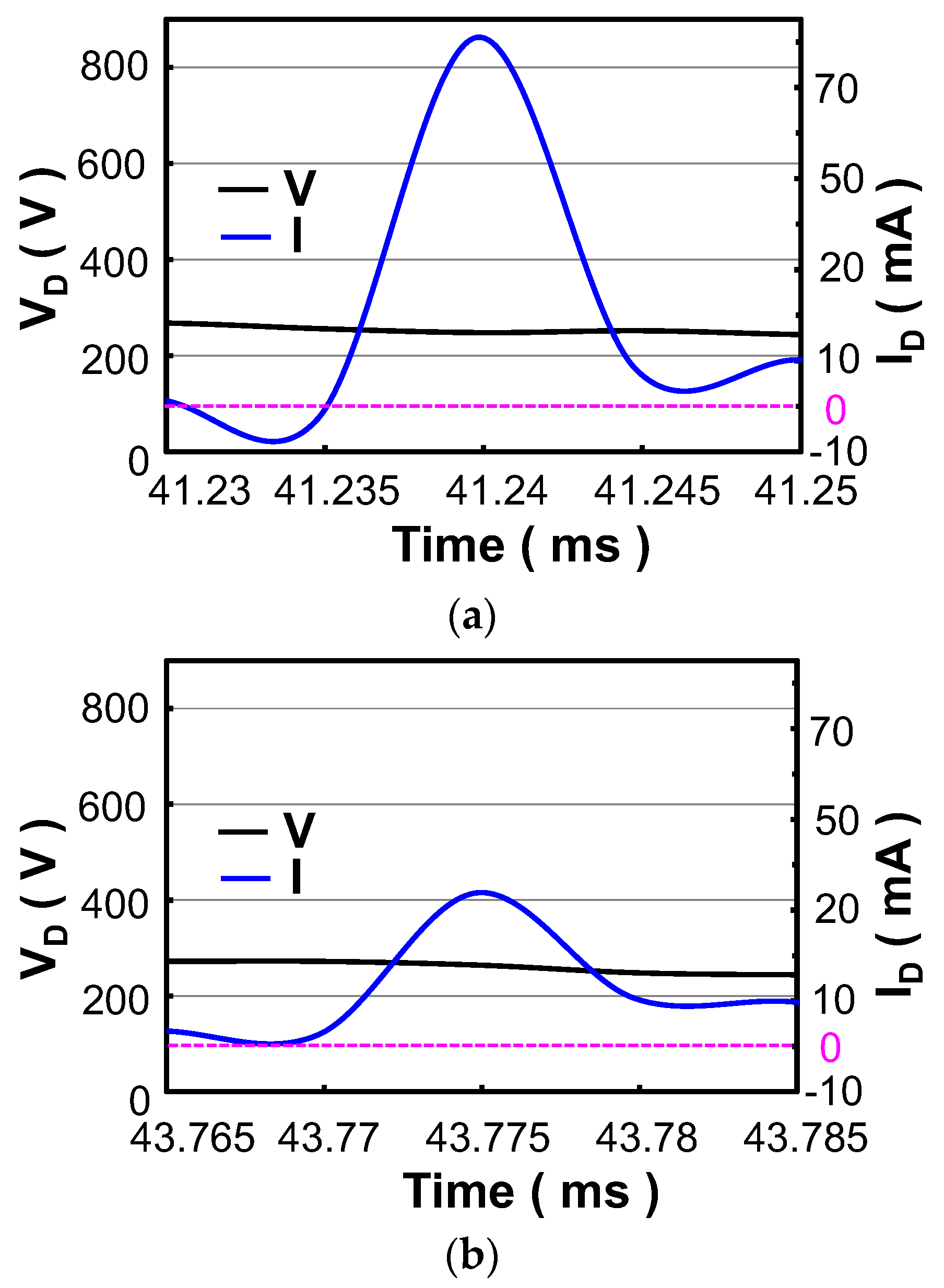
3.1. Measurement Result
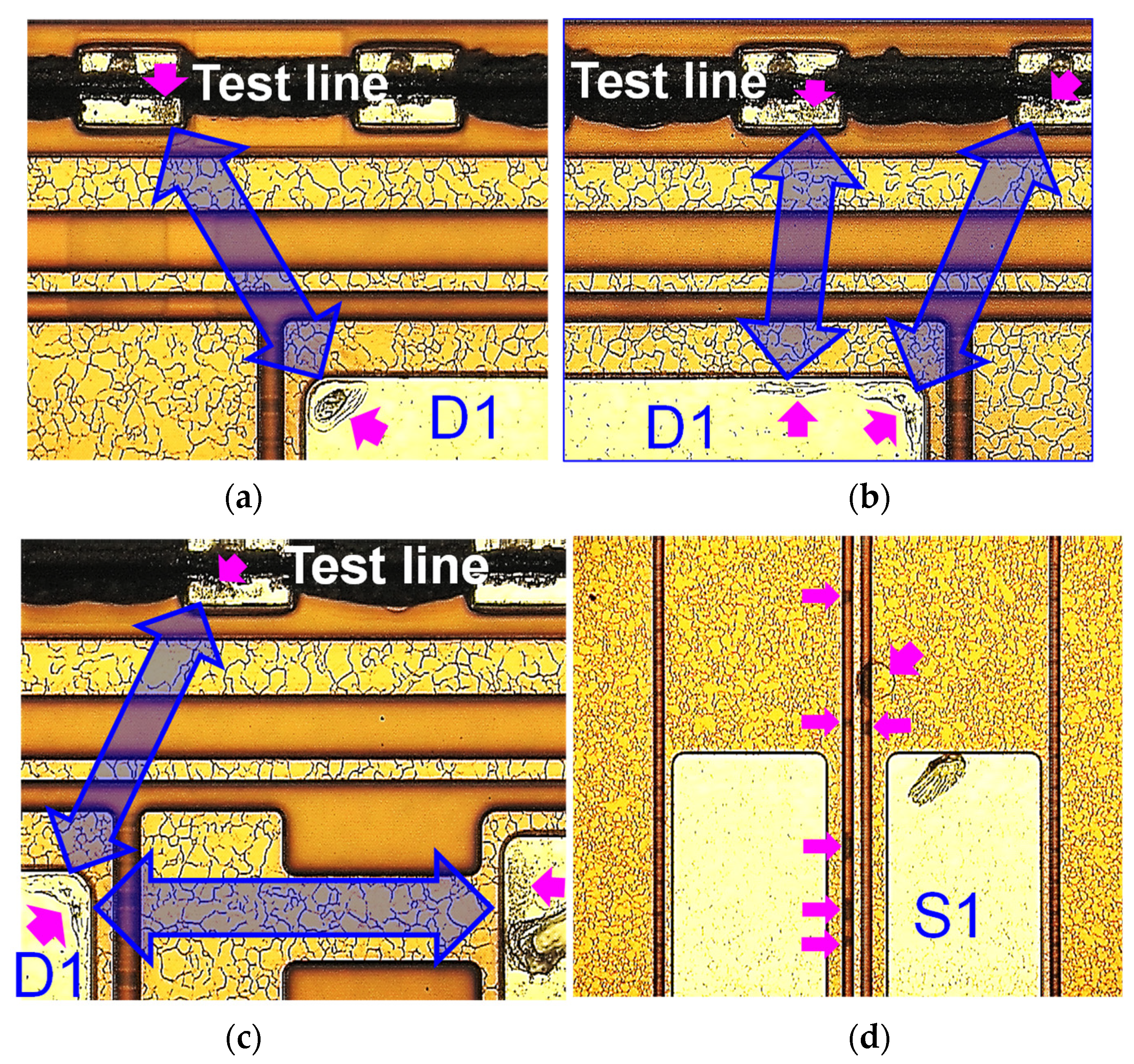
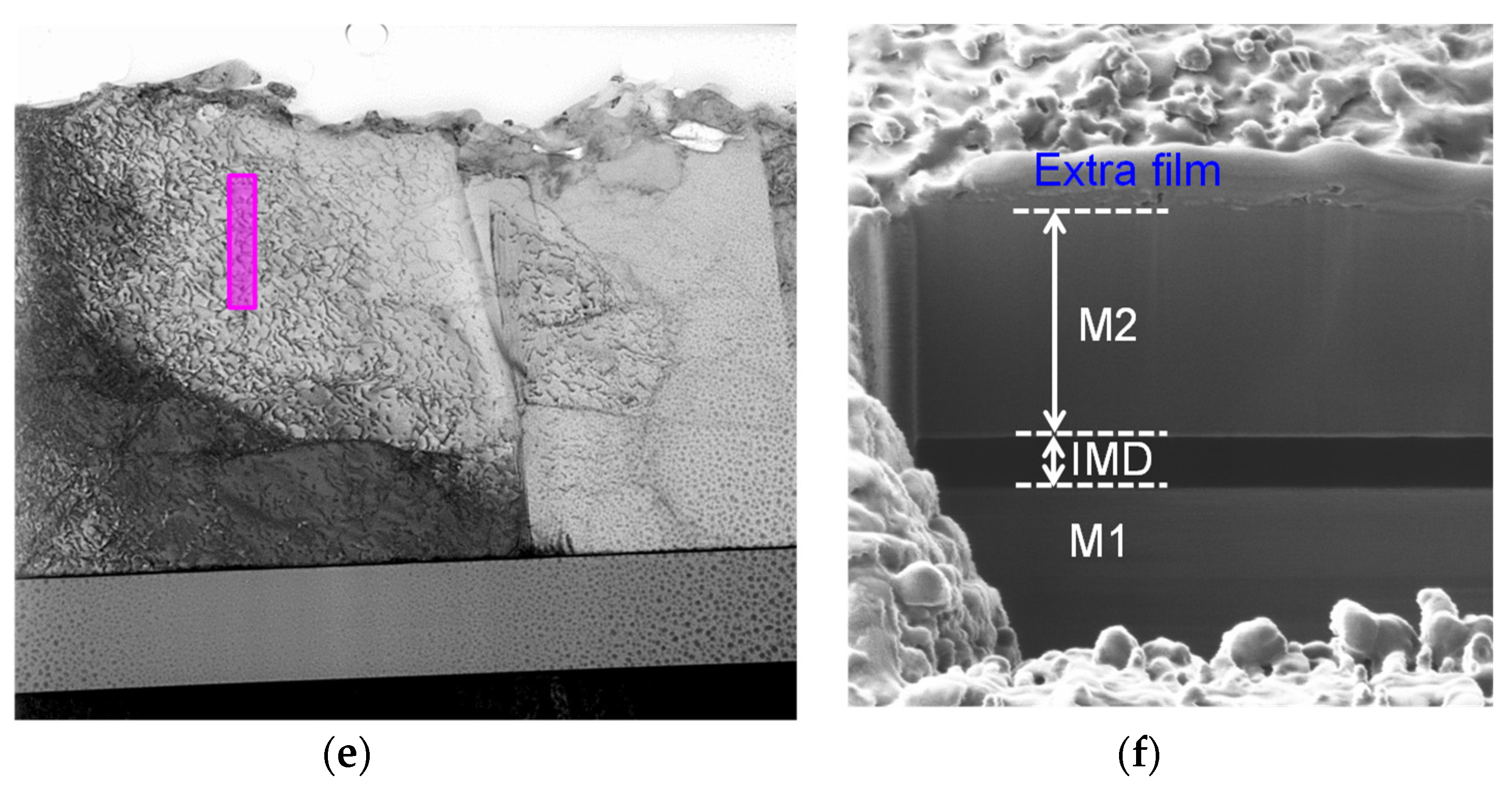
3.2. Failure Analysis Result
4. Discussion
5. Conclusions
Author Contributions
Funding
Institutional Review Board Statement
Informed Consent Statement
Data Availability Statement
Conflicts of Interest
References
- Slepian, J. Abridgment of extinction of an A-C. arc. J. Am. Inst. Electr. Eng. 1928, 47, 706–710. [Google Scholar] [CrossRef]
- Tanberg, R. On the cathode of an arc drawn in vacuum. Phys. Rev. 1930, 35, 1080–1089. [Google Scholar] [CrossRef]
- Cobine, J.D.; Power, R.B. The application of Paschen’s law to the re ignition of an Arc. J. Appl. Phys. 1937, 8, 287–290. [Google Scholar] [CrossRef]
- Browne, T.E. A study of A-C Arc behavior near current zero by means of mathematical models. Cond. Affect. Success Main Line Electrif. 1948, 67, 141–153. [Google Scholar] [CrossRef]
- Perkins, J.F.; Parker, A.B. Mechanism of dielectric recovery in uniform- and nonuniform-field gaps after high-current and high-pressure spark discharges. Proc. Inst. Electr. Eng. 1970, 117, 1460–1466. [Google Scholar] [CrossRef]
- Morshuis, P.H.F.; Smit, J.J. Partial Discharges at DC: Their mechanism, detection and analysis. IEEE Trans. Dielectr. Electr. Insul. 2005, 12, 328–340. [Google Scholar] [CrossRef] [Green Version]
- Bartnikas, R. A Commentary on Partial Discharge Measurement and Detection. IEEE Trans. Dielectr. Electr. Insul. 1987, EI-22, 629–653. [Google Scholar] [CrossRef]
- Alexander, P.; Uwe, S. Partial Discharge Measurement at DC Voltage-Evaluation and Characterization by NoDi Pattern. IEEE Trans. Dielectr. Electr. Insul. 2018, 25, 883–890. [Google Scholar]
- Hossein, D.I.; Mohammad, H.S.; Reza, Y. Generation of acoustic-resolved partial discharge patterns by utilizing UHF signals. Electr. Power Energy Syst. 2019, 113, 906–915. [Google Scholar]
- Edels, H.; Whittaker, D.; Evans, K.; Shaw, A. Experiments and theory on arc reignition by spark breakdown. Proc. Inst. Electr. Eng. 1965, 112, 2343–2352. [Google Scholar] [CrossRef]
- Boggs, S.A. Partial Discharge: Overview and signal generation. IEEE Electr. Insul. Mag. 1990, 6, 33–39. [Google Scholar] [CrossRef]
- Pedersen, A.; Crichton, G.C.; Mcallister, I.W. The theory and measurement of partial discharge transients. IEEE Trans. Dielectr. Electr. Insul. 1991, 26, 487–497. [Google Scholar] [CrossRef]
- Gutfleisch, F. Measurement and simulation of PD in Epoxy Voids. IEEE Trans. Dielectr. Electr. Insul. 1995, 2, 729–742. [Google Scholar] [CrossRef]
- Niemeyer, L. A generalized approach to partial discharge modeling. IEEE Trans. Dielectr. Electr. Insul. 1995, 2, 510–528. [Google Scholar] [CrossRef] [Green Version]
- Gafvert, U.; Edin, H.; Forssen, C. Modeling of partial discharge spectra measured with variable applied frequency. Proc. Int. Conf. Proper. Appl. Dielectr. Mater. 2003, 3, 839–842. [Google Scholar]
- Robson, A.E.; Thonemann, P.C. An Arc maintained on an isolated metal plate exposed to a plasma. Proc. Phys. Soc. 1959, 73, 508–512. [Google Scholar] [CrossRef]
- Schwirzke, F.; Taylor, R.J. Surface damage by sheath effects and unipolar arcs. J. Nucl. Mater. 1980, 93–94, 780–784. [Google Scholar] [CrossRef]
- Schwirzke, F. Unipolar arc model. J. Nucl. Mater. 1984, 128, 609–612. [Google Scholar] [CrossRef]
- Herman, J.G.; Daniel, C.S. Unipolar arc model. IEEE Trans. Plasma Sci. 1990, 18, 127–133. [Google Scholar]
- Schwirzke, F. Vacuum breakdown on metal surface. IEEE Trans. Plasma Sci. 1991, 19, 690–696. [Google Scholar] [CrossRef]
- Schwirzke, F.; Michael, P.H., Jr.; Xavier, K.M. Onset of breakdown and formation of cathode spots. IEEE Trans. Plasma Sci. 1993, 21, 410–415. [Google Scholar] [CrossRef]
- Tipirneni, N.; Koudymov, A.; Adivarahan, V.; Yang, J.; Simin, G.; Khan, M.A. The 1.6-kVAlGaN/GaN HFETs. IEEE Electron Device Lett. 2006, 27, 716–718. [Google Scholar] [CrossRef]
- Dora, Y.; Chakraborty, A.; Mccarthy, A.; Keller, S.; Denbaars, S.P.; Mishra, U.K. High breakdown voltage achieved on AlGaN/GaN HEMTs with integrated slant field plate. IEEE Electron Device Lett. 2006, 27, 713–715. [Google Scholar] [CrossRef]
- Zeng, K.; Vaidya, A.; Singisetti, U. 1.85 kV breakdown voltage in lateral field-plated Ga2O3 MOSFETs. IEEE Electron Device Lett. 2018, 39, 1385–1388. [Google Scholar] [CrossRef]
- Christophorou, L.G.; Pinnaduwage, L.A. Basic physics of gaseous dielectrics. IEEE Trans. Dielectr. Electr. Insul. 1990, 25, 55–74. [Google Scholar] [CrossRef]
- Fruth, B. Partial discharge mechansims in solid insulation systems. In Proceedings of the 4th International Conference on Conduction and Breakdown in Solid Dielectrics, Sestri Levante, Italy, 22–25 June 1992. [Google Scholar]
- Frederik, H.K.; Udo, F. Partial Discharges in Gaseous Voids for DC Voltage. Jpa. J. Appl. Phys. 1994, 33, 1079–1084. [Google Scholar]
- Xiaohua, Z.; Bo, P.; Yaxin, L.; Shaoyu, L.; Peng, X.; Yan, L.; Yifan, L.; Leijie, Q.; Qing, X. Review on Detection of Partial Discharge along Power Cables. Energies 2021, 14, 7692. [Google Scholar]
- Chuanyang, L.; Tohid, S.; Mohamadreza, A.B.; Kerry, D.; Yang, C.; Di, Z. Understanding DC Partial Discharge: Recent Process, Challenges and Outlooks. CSEE J. Power Energy Syst. 2022, 8, 894–908. [Google Scholar]
- Lee, J.H.; Huang, Y.J.; Hong, L.Y.; Chen, L.F.; Jou, Y.N.; Lin, S.C.; Wohlmuth, W. Incorporation of a simple ESD circuit in a 650V E-mode GaN HEMT for all-terminal ESD protection. In Proceedings of the 2022 IEEE International Reliability Physics Symposium (IRPS), Dallas, TX, USA, 27–31 March 2022. [Google Scholar]
- Slade, P.G.; Taylor, E.D. Electrical breakdown in atmospheric air between closely space (0.2 μm–40 μm) electrical contacts. Trans. Compon. Packag. Manuf. Technol. 2002, 25, 390–396. [Google Scholar] [CrossRef]
- Lee, J.H.; Iyer, N.M.; Jain, R.; Prabhu, M. Predictive high voltage esd device design methodology. In Proceedings of the 2016 38th Electrical Overstress/Electrostatic Discharge Symposium (EOS/ESD), Garden Grove, CA, USA, 11–16 September 2016; pp. 1–8. [Google Scholar]
- Lee, J.-H.; Iyer, N.M. Tunable holding-voltage high voltage ESD devices. In Proceedings of the 2019 IEEE International Reliability Physics Symposium (IRPS), Monterey, CA, USA, 31 March–4 April 2019; pp. 1–8. [Google Scholar]
- Lee, J.H.; Liu, W.Y.; Huang, C.Y.; Lo, K.H.; Yu, K.H.; Chiu, C.W. The Failure Mechanism of the E-SOA Boundary of Power Transistor Collapsed at Higher Gate Voltage. In Proceedings of the 2021 IEEE International Symposium on the Physical and Failure Analysis of Integrated Circuits (IPFA), Singapore, 29 November 2021. [Google Scholar]
- Lee, J.-H.; Liu, W.-Y.; Hung, C.-Y.; Lo, K.-H.; Yu, K.-H.; Chiu, C.-W. Failure mechanism of the power-clamp device of buck converter during the voltage conversion. In Proceedings of the 2020 IEEE International Symposium on the Physical and Failure Analysis of Integrated Circuits (IPFA), Singapore, 20–23 July 2020; pp. 1–6. [Google Scholar] [CrossRef]
- Lee, J.-H.; Nidhi, K.; Hung, C.-Y.; Liao, T.-W.; Liu, W.-Y.; Su, H.-D. Hysteresis effect induces the inductor power loss of converter during the voltage conversion. In Proceedings of the 2021 IEEE International Symposium on the Physical and Failure Analysis of Integrated Circuits (IPFA), Singapore, 15 September–15 October 2021; pp. 1–7. [Google Scholar] [CrossRef]


Publisher’s Note: MDPI stays neutral with regard to jurisdictional claims in published maps and institutional affiliations. |
© 2022 by the authors. Licensee MDPI, Basel, Switzerland. This article is an open access article distributed under the terms and conditions of the Creative Commons Attribution (CC BY) license (https://creativecommons.org/licenses/by/4.0/).
Share and Cite
Lee, J.-H.; Liao, C.-C.; Huang, Y.-J.; Li, C.-H.; Hong, L.-Y.; Jou, Y.-N.; Chen, K.-H. Unipolar Arc Ignited Partial Discharge for 650-V AlGaN/GaN HEMTs during the DC Breakdown Voltage Measurement. Energies 2022, 15, 7608. https://doi.org/10.3390/en15207608
Lee J-H, Liao C-C, Huang Y-J, Li C-H, Hong L-Y, Jou Y-N, Chen K-H. Unipolar Arc Ignited Partial Discharge for 650-V AlGaN/GaN HEMTs during the DC Breakdown Voltage Measurement. Energies. 2022; 15(20):7608. https://doi.org/10.3390/en15207608
Chicago/Turabian StyleLee, Jian-Hsing, Chih-Cherng Liao, Yeh-Jen Huang, Ching-Ho Li, Li-Yang Hong, Yeh-Ning Jou, and Ke-Horng Chen. 2022. "Unipolar Arc Ignited Partial Discharge for 650-V AlGaN/GaN HEMTs during the DC Breakdown Voltage Measurement" Energies 15, no. 20: 7608. https://doi.org/10.3390/en15207608