Abstract
An emerging area of interest within photovoltaic (PV) centred research is the simulation of the propagation of electromagnetic interference (EMI) and surges within PV installations. An overarching constraint in all simulation-based research is the accuracy of the models employed. In general, for PV-focussed simulations, nonlinear models are utilised for direct current (DC) analyses, whilst linearised models are employed for analyses involving surges or conducted electromagnetic interference. For large-signal electromagnetic interference and surges, the following two problems arise: (1) the aforementioned linearisation is only valid for the small-signal case, and (2) as they are constructed using only DC measurements, traditional large-signal PV models are generally only valid for DC conditions. Therefore, neither of these approaches can properly represent real-world PV behaviour under dynamic conditions. To overcome this limitation, this article proposes a more suitable model, compatible with Simulation Program with Integrated Circuit Emphasis (SPICE), and which results from the combination of two sub-models: one for large-signal DC cases, and one for small-signal alternating current (AC) cases. Consequently, the combined model enables improved modelling of the effects of large-signal transient perturbations to be performed, as well as cases involving small-signal AC and large-signal DC perturbations. The model parameters are extracted using data from two different classes of measurement setups: the first utilised a vector network analyser (VNA) to produce small-signal AC impedance results (covering a frequency range between 1 Hz and 50 MHz), and the second produces DC current-voltage curves. Both classes of measurement setup consider the device under test at multiple operating points. Key results include: (1) an improved SPICE-compatible PV model which caters for large-signal transient simulations, as well as for small-signal AC and large-signal DC cases, (2) improvements in the modelling of reverse bias behaviour when compared to the standard SPICE diode implementation, (3) the correct implementation of a voltage-dependent total capacitance (suitable for large-signal simulations), (4) modelling parameters for both a small (10 W) and a large (310 W) PV module, (5) measurement results which de-embedded the parasitic effects of the test setups employed, and (6) above 1 MHz, the physical layouts of the cells within the PV modules begin to influence the observed impedances.
Keywords:
electromagnetic; interference; compatibility; lightning; surge; simulation; transient; photovoltaic 1. Introduction
With the advent of economically-feasible large scale solar photovoltaic (PV) based electricity generation, much research on the modelling of such systems has been performed in recent years. More accurate modelling enables power producers to better forecast the energy yield of potential power plants prior to construction. These energy forecasts can, for example, be used to assess the ability of a proposed power plant to service the energy requirements of its clients, or, they can be incorporated within economic models in order to project the financial implications of a particular project. Although, understandably, energy-centric models comprise the largest proportion of all PV models, they are not the only type of model to see increasing interest of late.
2. Background
The following three subsections introduce concepts which are central to the research focus of this article.
2.1. Background Concept 1: Electromagnetic Compatibility
One area of emerging research examines the electromagnetic compatibility (EMC) aspects of PV installations—this is the overall domain within which this article focusses. The concept of EMC is achieved when a device is able to function “satisfactorily in its electromagnetic environment without introducing intolerable disturbances” [1]. This typically involves three facets: susceptibility, emissions, and coupling.
Susceptibility studies, such as in [2] or [3], for example, may involve the simulation of the propagation and resulting effects of small- and large-signal surges within PV installations. These surges could be caused by electrical fault conditions (either from within the installations themselves, or originating from the grid to which the PV installation is connected), or by external environmental stimuli (such as a direct lightning strike to the installation).
Emissions refers to the generation of electromagnetic energy by a device or installation, and is generally less of a concern for utility-scale PV installations as the chosen equipment typically complies to an accepted EMC standard (such as [4]), and does not produce interference which would hamper the correct operation of other nearby equipment. An exception, however, is where nearby equipment may be particularly sensitive to electromagnetic interference (EMI). One example of where EMI mitigation strategies had to be employed in order to attain EMC is the Australian Square Kilometre Array Pathfinder (ASKAP) hybrid solar-diesel power station, which was designed in such a way so as not to interfere with the ASKAP and Murchison Widefield Array (MWA) radio telescopes [5].
Coupling studies can be more nuanced, and, for example, may investigate the susceptibility of a PV installation as a result of the coupling between a radiating electromagnetic source (such as a nearby lightning strike) and the PV installation. This particular topic is investigated using a high-current pulse generator in [6,7]. It is investigated in [8] by mathematically deriving a circuit representation of a lightning-channel-to-PV-module coupling model, and then including this within a circuit simulation. In [9], the partial element equivalent circuit method (PEEC) is used to produce a circuit representation of the coupling between an actual PV plant and an overhead high-voltage transmission line—the measured and simulated results are then compared.
The aforementioned topic has also been investigated using computational electromagnetic (CEM) simulation packages. For example, CEM results for the induced currents within a single PV module are compared with those from a high-voltage laboratory in [10]. These CEM results are then extended to a four-module array in [11]. More cases, including examination of the induced voltages, as well as mitigation strategies, are investigated in [12]. This type of simulation produces results which are heavily dependent on the accuracy of the impedances of the models employed—especially if the simulations cover a wide bandwidth. The inclusion of nonlinear devices, of which a PV cell is an example, further increase the complexity of the simulations. For a truly comprehensive simulation of this nature, a full-wave 3D CEM simulation needs to be combined with a nonlinear circuit model—this has not been done yet. CST is an example of a CEM software package which offers a circuit solver—similar to Simulation Program with Integrated Circuit Emphasis (SPICE)—which it can (unidirectionally or bidirectionally) couple to its electromagnetic solvers [13]. It is for this compatibility reason that a SPICE implementation was selected for this study, and an appropriate circuit model is the first step in creating a model which accurately links external electromagnetic stimuli to induced currents and voltages.
In order to begin the process of constructing a suitable circuit model for this particular purpose, the following subsection covers the state-of-the-art of PV circuit modelling.
2.2. Background Concept 2: Circuit PV Modelling State-of-the-Art
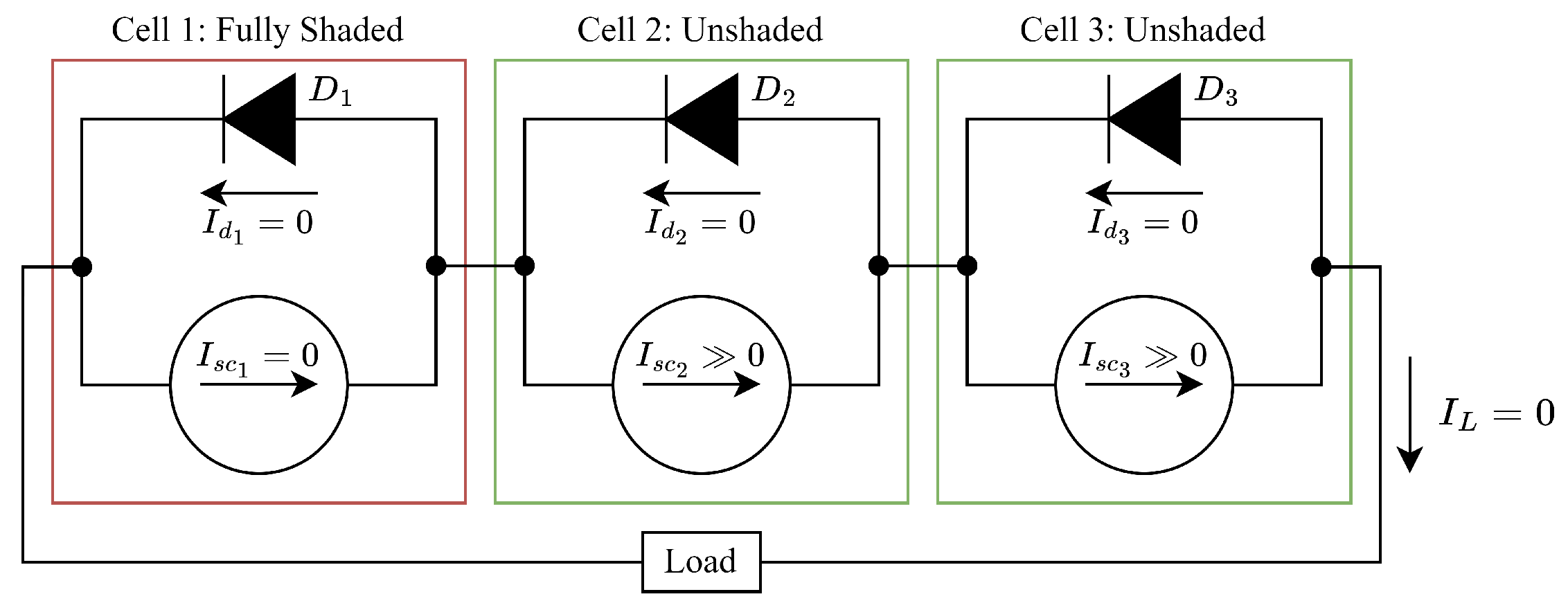
When employing circuit simulations for EMC-centred purposes, adequate component model accuracy is pivotal. The most simple circuit which is representative of PV cell operation is put forward by [14] and comprises a real diode, D, in parallel with a current source, . This current source represents the photocurrent, and the magnitude of the current corresponds to the level of irradiance that the PV cell is exposed to. PV cells are only able to produce around 0.6–0.7 V [14]. Therefore, in practice, multiple cells are generally connected in series. For weatherising purposes, these series-connected cells are often covered by a glass pane, which is surrounded by an aluminium frame—thus forming a PV module. Multiple series-connected modules form a string. When considering the series-connected nature of modules and strings, a quandary arises: how does the aforementioned model respond when different cells are exposed to different irradiance intensities—such as with full or partial-shading? This issue is demonstrated in Figure 1, where when the cells experience differing levels of solar irradiance. As each diode would be reverse biased in this circumstance, zero current would flow through each of the real diodes (i.e., ). Thus, the total module (and string) current would be zero, as would the current delivered to the load, . Consequently, the power produced by the string, as well as the power delivered to the load, would also be zero. In practice, this is not the case; therefore, a more representative model is needed.
The single diode model (SDM) circumvents this issue by including a parallel resistance, , to model a P-N junction leakage current, [15]. Furthermore, the resistances of the wire leads (connected to the PV cells), as well as the contact resistances between the wire leads and the PV cells, are modelled by a series resistance, , which conducts a current [14,15]. The extraction of the SDM parameters has been the subject of much research. A well-cited example of this is [16], where the authors propose and demonstrate the accuracy of a convenient method for extracting the SDM parameters using datasheet parameters at the following points: (1) open-circuit, (2) short-circuit, and (3) maximum power. Furthermore, as a PV installation is generally expected to function for multiple decades, PV models for long-term yield forecasting purposes should also consider the effects of PV cell ageing; [17] investigates the impact of changes in the ideality factor (due to changes in and ) on power production. For completeness, it is noted that the current path through a fully-shaded PV cell provided by introduces a practical problem—heat. Current forced through a shaded PV cell is dissipated as heat. This is referred to as the hotspot phenomenon, which results in both a decrease in the total power production of a module or string, and also a risk of permanent damage to the shaded PV cell should a threshold (known as the critical power dissipation, ) be reached.
To circumvent this issue, a bypass diode may be incorporated. This diode, usually a Schottky diode, is placed parallel to a cell or module to provide an alternative current path in instances of shading [18]. Figure 2 illustrates this concept—where three PV cells (each depicted by an instance of the SDM) are shown, each in parallel with their own bypass diode, . The current through a bypass diode is represented by .

Figure 2.
A demonstration of the function of bypass diodes. Three series-connected PV cells are represented by separate instances of the single diode model (SDM), and are not all subject to the same irradiance levels. Each PV cell is placed in parallel with a separate bypass diode. Developed from [18].

Figure 1.
Current inconsistency encountered with the simplest photovoltaic (PV) cell model during instances of differing solar irradiance. Developed from [18].
Alternative PV models, such as the two diode model, are sometimes employed to either increase the simulation accuracy (as in [19]) or to reduce the computational load (as in [20]). The models discussed thus far, however, are only valid for direct current (DC) conditions (i.e., a single operating point).
For alternating current (AC) conditions, the model shown in Figure 3 is often referenced [8,21,22]. This model, referred to in this article as the small-signal AC sub-model (SSACSM), incorporates a parallel capacitance, , and a series inductance, , to model the PV cell response under dynamic conditions. models the effect of junction, diffusion, and breakdown capacitance—which are all nonlinearly dependent on the operating point and temperature [21]. These capacitances also dominate at different operating points.

Figure 3.
Circuit schematic of the small-signal AC sub-model. Developed from [21].
Junction capacitance is dominant at small positive and negative voltages; diffusion capacitance is dominant above the maximum power point voltage; and breakdown capacitance is dominant when the cell experiences reverse breakdown [21]. models the series inductance of the wire leads connected to the PV cells [21]. Other parameters, such as , , and from the SDM, are linearised and replaced by a single equivalent resistance . As both and are dependent on the voltage across the P-N junction, , as well as environmental conditions (such as temperature and the level of solar irradiance) this model is only valid for small-signal perturbations [21]. Voltage refers to the voltage at the output terminals for this small-signal case. Even assuming constant environmental conditions, a large-signal perturbation would result in a change in , requiring subsequent parameter changes of and . One particular strength of this model is its usefulness in the extraction of circuit parameters which either do not, or negligibly, change with environmental conductions (e.g., and ). Therefore, they can be derived using a small-signal-based measurement setup.
Figure 4, adapted from and put forward by [21], illustrates a dynamic PV cell model which implements a variable capacitance, , that adjusts with bias voltage and environmental conditions, as does the photocurrent, . Voltage refers to the instantaneous voltage at the output terminals. This model also aims to improve the reverse bias accuracy of the model with the inclusion of a reverse-biased diode, , the operation of which is offset by a DC voltage, . This model, implemented in MATLAB [23] by the authors, offers sufficient abstraction from the underlying semiconductor physics without overly compromising simulation accuracy for practical purposes. In [21], DC parameters were extracted using a DC source, and unbiased AC parameters were extracted using a signal generator and an oscilloscope. DC-biased AC parameters were extracted using a combination of the aforementioned instruments, as well as an isolation transformer, in order to allow for the simultaneous application of both an AC and a DC signal. Three frequency points were used: was extracted at 500 Hz, was extracted at 100 kHz, and was extracted at 1 MHz [21]. Due to its MATLAB-based implementation in [21], this model is difficult to combine with a CEM simulation—which, as initially explained in Section 2.1, is the next goal of this line of research. Furthermore, the lack of measured phase information and the risk of sampling complexities (explained later, in Section 3.2.1) supported the need for the research documented in this article.

Figure 4.
An example of a photovoltaic model which incorporates voltage-dependent capacitance, as well as improved reverse-bias, characteristics. Developed from [21].
This section introduced the commonly-used circuit models for PV cell, module, and array modelling under different conditions. However, when producing a circuit model for the behaviour of a geometrically-complex circuit, especially at high frequencies, one has to consider the possibility of the presence of undesirable circuit elements. These are discussed in the following section.
2.3. Background Concept 3: Undesirable Circuit Elements
In this article, an undesirable circuit element refers to a circuit element which results in unintended operation of the device under test (DUT). Three types of undesirable circuit elements are introduced: parasitic, radiating, and mutually-coupled.
A parasitic element is an unintended and somewhat-unavoidable circuit element which possesses undesirable characteristics. For example, a circuit designer may wish to make use of a typical through-hole technology (THT) capacitor in their circuit. A practical capacitor, however, does not only possess a capacitance (as is the case for an ideal/theoretical capacitor). Individually, wire leads will have both resistance and inductance. A parasitic capacitance will also form between the wire leads. This concept is illustrated in Figure 5 below, where the ideal capacitance is represented by , and the parasitic inductances, resistances, and capacitance are represented by , , and , respectively.
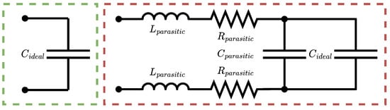
Figure 5.
An ideal capacitor (left) and a real capacitor (right).
The circuit designer may expect the impedance of the real capacitor to decrease as frequency increases, however, if the parasitic inductances are great enough that the ideal capacitance no longer dominates the overall impedance, then the circuit designer will discover that the capacitor behaves more like an inductor at high frequencies. The influence of the parasitic elements, can, however, be diminished by paying attention to the component choice and layout. In the example of the THT capacitor, the wire leads can be shortened prior to installation in order to decrease the parasitic inductances, resistances, and capacitances. Parasitic elements may or may not be within the control of a circuit designer, however, their presence should always be considered if they noticeably influence the operation of the designed circuit.
The second type of undesirable circuit element discussed here is a radiating element. This type of element directly radiates electromagnetic energy. In this case, the DUT may become resonant and actively radiate energy in the form of electromagnetic waves—thereby acting as an (unintentional, in this case) antenna. This may happen as physical size of conductive pathways within the DUT become similar to the wavelengths involved in the testing. Figure 6 illustrates this concept. In this figure, a DUT is being analysed by a VNA. The VNA produces a signal and interprets the reflected signal of the DUT in order to obtain the desired parameter(s). The DUT, however, contains a radiating element, which broadcasts electromagnetic energy to space. In the context of a transmitting antenna, optimal radiation is desirable. However, an unintentional antenna in an electromagnetically-sensitive environment, such as the area near the aforementioned ASKAP radio telescopes, would be consequential.

Figure 6.
The concept of a radiating element in the context of a vector network analyser (VNA)-based measurement of a device under test (DUT).
Finally, the concept of mutual coupling is introduced. Mutual coupling describes the electromagnetic interaction between circuit elements. This is the core concept in a transformer, where a primary coil produces an electromagnetic field which couples into, and produces a response, in the secondary coil—exploiting the concept of mutual inductance (generally referred to by parameter M). Figure 7 illustrates this concept, where and represent the self inductance of the primary and secondary coils, respectively, and M represents the mutual inductance between the coils.
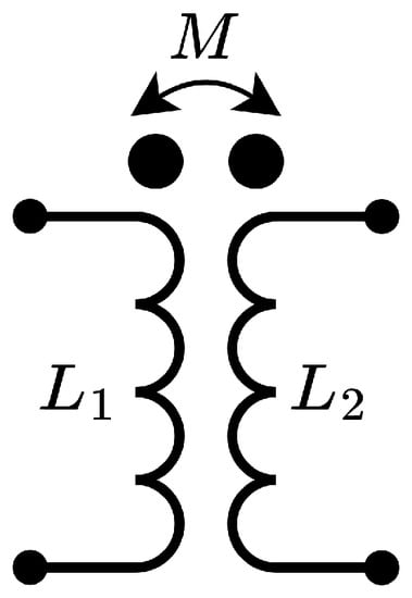
Figure 7.
An inductor-based example of the concept of mutual coupling.
The concept of layout-based parasitic elements, radiating elements, and mutually-coupled elements becomes applicable later, in the results section (Section 5). The following subsection introduces the particular PV modules selected for this study.
2.4. Studied PV Modules and Motivation
A large and a small PV module, shown in Figure 8, were selected for this study in order to assist readers in choosing the circuit modelling parameters most appropriate for their particular application. The most-used datasheet parameters of both PV modules are included in Table 1 below.

Figure 8.
The large (left) and the small (right) PV modules.

Table 1.
Datasheet parameters for the large and small PV modules.
The large PV module, a BYD 310P6C-36 (BYD Co. Ltd., Shenzhen, China), is composed of 72 series-connected polycrystalline PV cells [24]. This topology is seen in many utility-scale PV power plants around the world. Within this module, a bypass diode is generally placed in parallel with every 24 cells. However, for this study, the bypass diodes were detached from the module in order to remove their effect on the measured impedance between the output terminals. For completeness, nonlinear dynamic modelling of bypass diodes is covered in detail in [18].
The small PV module, an ACDC SLP005-12 (ACDC Dynamics, Edenvale, South Africa), is composed of 36 series-connected polycrystalline PV cells [25]. This smaller class of PV module is often used in off-grid outdoor lighting and Internet of Things (IoT) based applications, where little power is required yet no method of convenient grid integration exists. This module does not include any bypass diodes.
This section provided the necessary background information for this study. Firstly, the concept of EMC was introduced—including an explanation of the need for accurate circuit models in CEM simulations. Secondly, existing models for PV cells, modules, and arrays under DC, small-signal AC, and transient conditions were discussed—including their shortcomings. Thirdly, the concept of undesirable circuit elements was introduced. Finally, an overview of the PV modules chosen for this study was presented. Altogether, this section highlighted the need for a circuit PV model which: (1) is SPICE-compatible, (2) able to handle both small-signal and large-signal stimuli. These two points became the primary objectives for this study. The following section discusses a proposed model for these two PV modules, suitable for use in SPICE.
3. Proposed Solution: Full Circuit PV Model (FCPVM)
This article proposes the SPICE compatible model shown in Figure 9. This model, referred to as the full circuit PV model (FCPVM), can be applied at the cell, module, or string scale. This model comprises the following components: a series inductance, , to model the inductive properties of the conductive inter-cell connections; a series resistance, , to model the resistive properties of the conductive inter-cell connections, as well as the resistive properties of the contact resistances between the inter-cell connections and the P-N junctions themselves; a nonlinearly voltage-dependent capacitance, , to model the overall capacitive properties (a combination of the junction, diffusion, and breakdown capacitances) of the P-N junction; a forward bias diode, , to model the nonlinear DC operation of the P-N junction in forward bias, a reverse bias diode, , to model the nonlinear DC operation of the P-N junction in reverse bias; and a current source, , which models the photocurrent resulting from exposure of the PV cells to solar irradiance. The FCPVM is formed by combining two sub-models, namely (1) the large-signal direct current sub-model (LSDCSM) and (2) the small-signal alternating current sub-model (SSACSM) (illustrated earlier in Figure 3). These sub-models are discussed in the following subsections.
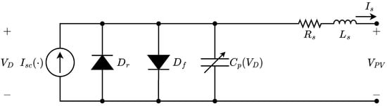
Figure 9.
Circuit schematic of the proposed full circuit PV model (FCPVM). Developed from [18].
3.1. The Large-Signal DC Sub-Model (LSDCSM)
For the DC case, |, and |. For this reason, element can be substituted with an open circuit, and element , can be substituted with a short circuit. Performing these amendments to the FCPVM results in the LSDCSM—shown in Figure 10.

Figure 10.
Circuit schematic of the large-signal DC sub-model (LSDCSM). Developed from [18].
The dual-diode implementation was used to circumvent the inherent shortcomings of the SPICE large-signal diode model (LSDM). This default SPICE model, which is illustrated in Figure 11 (and modelled after [26]), comprises the following elements: a resistance, ; a diode, ; and a conductance, . Element models the nonlinear operation of the diode. Element models the linear behaviour of the diode due to the effects of contact resistances between the diode junction and the leads connected to the junction, as well as the resistance of the leads themselves. Element exists to aid with the solver convergence [26].

Figure 11.
Circuit schematic of the SPICE large-signal diode model (LSDM). Developed from [26].
The current-voltage relationship of the SPICE LSDM is defined mathematically by Equations (1)–(4). The following definitions relate specifically to diode : represents the diode voltage, represents the reverse breakdown voltage, represents the saturation current, N represents the emission coefficient, represents the thermal voltage [26]. and represent the current through and voltage over the complete model.
For :
For :
For :
For :
Parameter is calculated using Equation (5). In Equation (5), k represents the Boltzmann constant, T represents the analysis temperature, and q represents the charge on an electron. For completeness, it should be noted that T is specified by the user in units of degrees Celsius (°C), and that SPICE automatically converts this value to the equivalent value in units of Kelvin (K) before inserting it into Equation (5). The parameters required for the calculation of the thermal voltage are listed in Table 2 below. The remaining parameters of the SPICE large-signal model, as well as their definitions, are listed in Table 3.
Table 2.
Default parameters for the calculation of the thermal voltage, , utilised in the SPICE LSDM. From [18,26].
Table 3.
Default parameters of the SPICE LSDM. From [18,26].
Figure 12 (adapted from [26]) illustrates the current–voltage relationship of the default SPICE LSDM. In this illustration, it is clear that this model considerably simplifies the current–voltage relationship in the reverse bias region, especially where is between and . When applying this SPICE model to a PV context, implementation of the SDM amends this response by including parameter in parallel with a diode junction—resulting in an offset linear current-voltage relationship in this specific region. The DC sub-model goes one step further, and instead of supplementing the default SPICE LSDM with a resistor, a second instance of the default SPICE LSDM, with opposing polarity, is added. This second instance represents element in the LSDM. The governing parameters of are adjusted such that the resulting combined response is more representative of actual PV reverse-bias operation than either a single default SPICE LSDM, or its parallel combination with a resistance, can achieve. This is demonstrated in Section 5.
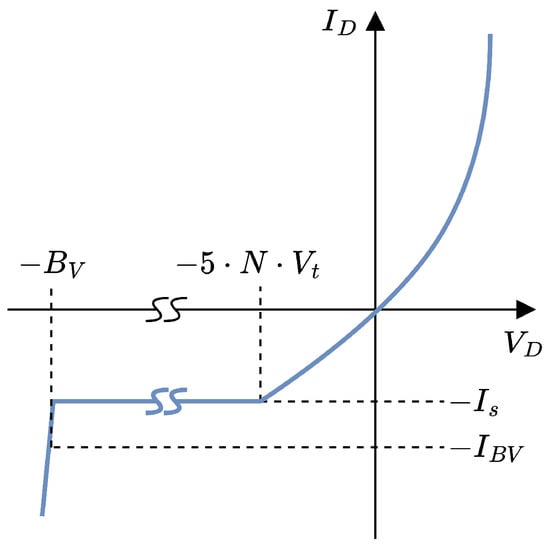
Figure 12.
A parametric illustration of the current–voltage relationship of the default SPICE LSDM. Developed from [18,26].
It is critical to note that the default SPICE LSDM fails to include either an inductance or a completely user-definable capacitance that is voltage-dependent—these are components that are key for simulations involving AC or transient conditions. These components can, however, easily be inserted using additional SPICE components. The following sub-model presents the inclusion of these components.
3.2. The Small-Signal AC Sub-Model (SSACSM)
Equation (6), below, derives an expression for the impedance of the SSACSM—this impedance is referred to as .
where
and f represents the frequency in Hertz (Hz).
3.2.1. Sampling Complexities
When measuring and modelling the impedance of a DUT, a few key points need to be considered.
As previously mentioned, the authors of [21] used a signal generator and an oscilloscope to measure PV cell impedances, which were then extracted mathematically. This technique is valid, however, it is critical that a comprehensive frequency sweep (across the intended frequency band for which the model is expected to function) is performed. This will allow the researcher to correctly identify areas within the magnitude of the impedance where particular circuit elements are dominant. Incorrect choice of sampling points, or too wide a frequency spacing, may result in inaccurate parameter values. To the credit of the authors of [21], this was done, however, it is imperative that this is done every time.
Furthermore, as the impedances of parasitic and radiating elements become more dominant as frequency increases, one should not over-extrapolate the measured data.
To illustrate the two above-mentioned concepts, was calculated using Python [27] for a frequency band between 1 and 50 . For this, the following hypothetical parameter values were used: was chosen as 1 Ω; was chosen as 30 kΩ; was chosen as 200 ; and was chosen as 300 . A parasitic capacitance of 1 was then added in parallel with the calculated impedance, producing an impedance which is referred to hereafter as the actual impedance. In practice, this small capacitance could represent the capacitance between two closely-positioned DC conductors which travel between a PV array and a maximum power point tracking (MPPT) input of a solar charge controller. Parameters , , and were then extracted at 500 Hz, 100 kHz, and 1 MHz, respectively. Parameter was extracted at the resonant point between regions of dominance between the parallel combination of and , and . Equation (6) was then calculated using the extracted parameters, producing an impedance which is referred to hereafter as the calculated impedance.
Magnitude and phase plots of the actual and calculated impedances, shown in Figure 13, were produced using the Matplotlib Python library [28].
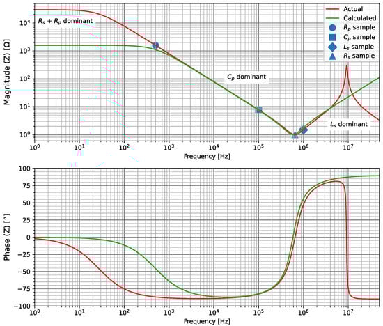
Figure 13.
Impedance curves for the small-signal AC sub-model (SSACSM), where the “actual” trace represents the true impedance of the DUT, and the “calculated” trace represents the reconstructed impedance. Good agreement is not shown. This illustrates the importance of: (1) correct sampling and (2) avoiding over-extrapolation.
For simplicity, the calculated impedance is analysed first. As expected, the magnitude plot decreases linearly (given logarithmic vertical and horizontal axes) where component dominates. Similarly, the magnitude increases linearly where component dominates. The magnitude is relatively constant at low frequencies, where dominates. At the resonant point between regions of dominance between the parallel combination of and , and , parameter dominates.
When comparing the magnitude of the calculated impedance to the magnitude of the actual impedance below 1 MHz, it is noticed that a poor choice of sampling frequencies resulted in a suboptimal model, particularly at low frequencies (as ) was sampled in a region where was dominant. Furthermore, was not absolutely dominant at 1 MHz, which produced a suboptimal fit at 1 MHz and beyond. was sampled in a region where was dominant, therefore the magnitudes of the calculated and actual impedances agree well in this region. In this case, correcting the choice of sampling frequencies would produce a relatively accurate model of the actual impedance below 1 MHz. This demonstrates the necessity of sampling the entire range of operation of the intended model.
Above 1 MHz, the influence of the 1 nF parasitic capacitance becomes dominant. Equation (6) does not cater for the influence of this additional element, therefore the calculated impedance cannot accurately follow the actual impedance in this region. Equation (6) suggests that the magnitude of the impedance would increase with frequency ad infinitum, whereas the inclusion of the parasitic capacitance prevents that as the magnitude of its impedance dominates that of element . Even if Equation (6) were to be amended to consider this element, then sampling at frequencies higher than 1 MHz would be required. This further demonstrates the necessity of sampling the entire range of operation of the intended model, and emphasises the risks of over-extrapolating measured data.
The discrepancy between the phases of the actual and calculated impedances further illustrates the effects of the above-mentioned issues. This emphasises the importance of considering all relevant components in order to ensure accurate simulation results.
The dynamic range of the measurement equipment should also be considered within the context of the measurement setup. For example, an oscilloscope and signal generator-based approach may not be able to accurately determine parameter due to the limited resolution and high noise floor. The lack of the ability to perform a calibration routine would also make exclusion of the parasitic elements of the test setup itself difficult. In this article, AC measurements conducted using a vector network analyser (VNA)—specifically an Omicron Lab Bode 100—which provides accurate magnitude and phase results. The specific measurement configurations are detailed later, in Section 4.
3.3. Voltage-Dependent Nonlinear Capacitance
The influence of element dominates the total impedance of a PV cell, , within a specific frequency band. In this band, the value of can be determined using the imaginary part of . For this, Equation (8) is used, where f represents the frequency in Hertz. For completeness, it is noted that, due to the dominance of a capacitive element, the term in Equation (8) is negative. This negative term is then cancelled out by the negative term in the numerator of Equation (8), thereby resulting in a positive value for the capacitance, .
P-N junction capacitance varies with the applied voltage [29]. Therefore, the capacitance should be measured over a range of DC bias levels. A mathematical expression is then fit to the measured results, as in [30]. This expression, however, is not yet suitable for direct implementation in large-signal SPICE simulations. A function, described in the following subsection, is first applied to the aforementioned expression to produce a voltage-dependent capacitance which correctly exhibits large-signal behaviour.
3.3.1. Implementation of a Voltage-Dependent Capacitance in SPICE
Once the circuit parameters have been obtained, the FCPVM can be constructed in SPICE. The particular SPICE-based simulation package used in this article is LTspice, which is produced by Analog Devices [31]. Components and are implemented using standard resistors, components and are implemented using separate instances of the default SPICE LSDM, and component is implemented using a standard inductor. Capacitor requires a more intricate implementation.
In general, a voltage-dependent capacitor could be defined in the following two manners: (1) the total capacitance, which is calculated as a function of the charge stored in the capacitor () and the applied voltage (v), as shown in Equation (9), and (2) the local capacitance, which is calculated as a (local) derivative of with respect to v, as shown in Equation (10) [30]. is generally derived from experiments involving charge injection, whereas is generally derived from experiments involving the a small-signal perturbation, superimposed on a DC voltage [30]. The latter describes the procedure used later in Section 5.2. Figure 14, adapted from [30], illustrates this discrepancy. It is clear that only for a non-voltage-dependent capacitor does hold, as the relationship between Q and V would be linear.
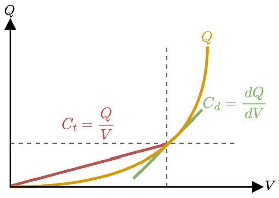
Figure 14.
The concepts of total capacitance () and local capacitance ().
In addition, if Equation (9) is rearranged such as to make the subject of the formula, and then differentiated with respect to time, t, this produces Equation (11)—where the current flowing through the capacitor is represented by i [30]. In the case of small-signal perturbations, one can ignore the second term in Equation (11). For the large-signal case, the full equation is required [30].
In [30], the following link between and is derived. First, the subject of Equation (10) is changed, forming Equation (12), which is then integrated with respect to v. This produces Equation (13). Substituting Equation (13) into Equation (9) produces Equation (14)—an expression which allows for the determination of using . This is particularly useful, as measurement data from small-signal-based methods can be utilised in large-signal applications [30]—negating the need for a charge injection-based measurement method.
Now that (1) a method of sampling the local capacitance of a PV cell has been presented, and (2) a method of converting the sampled capacitance to the total capacitance (given its voltage–dependent nature), the resulting total capacitance can be implemented in LTspice. For this, the current source-based technique, suggested by [30], is employed.
In this technique, Equation (11) is used to control a behavioural current source. This behavioural current source is labelled C_p in Figure 15, which illustrates the LTspice implementation of the FCPVM, below. The DDT operator in LTspice is used to realise the terms in Equation (11). A separate circuit, comprising a resistor and a behavioural voltage source, and shown on the right of Figure 15, is then utilised to implement the voltage–dependent capacitance. The voltage of this behavioural voltage source, labelled C_Rep, is controlled by the calculated total capacitance curve, using the voltage over element C_p (i.e., (V+) – V(Cathode)) as its input. Element C_Rep then produces a voltage value representing the desired capacitance (i.e., ), which is then used as an input to element C_p, along with the value of the voltage over element C_p. The value of element R_Cap is irrelevant in the abovementioned calculations, so long as it is greater than zero. Parameters {alpha} and {beta} in Figure 15 relate to constants within the calculated total voltage–capacitance curve, and are covered later in Section 5.2.
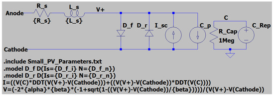
Figure 15.
The FCPVM, implemented in LTspice. Developed from [18].
For ease-of-use, the required parameters can be included within a text file, such as in Figure 16, that is imported once per simulation run. Furthermore, the circuit in Figure 15 can be represented by a sub-circuit element in LTspice, as in Figure 17.
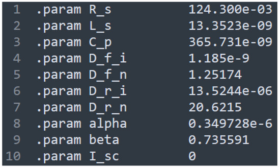
Figure 16.
An example of a text file, which includes the necessary FCPVM parameters (for the large PV module, in this case), which is imported by LTspice once per simulation run.

Figure 17.
An example of how a custom symbol may be used to represent a sub-circuit (in this case, the FCPVM from Figure 15). Developed from [18].
Table 4 summarises the suitability of the models discussed thus far which are suitable for direct implementation in SPICE (enabling their use in a future CST CEM simulation).
Table 4.
Summarising the suitability of the examined SPICE-compatible circuit PV models within different contexts.
As the FCPVM, including its origins and LTspice implementation, have been discussed, the article will now introduce the multitude of measurement setups utilised to obtain the necessary model parameters.
4. Experimental Tests
The two PV modules are examined using two classes of measurement setups. The first class of measurement setup utilises small-signal AC measurements. The second class of measurement setup utilises large-signal DC measurements. Two sub-classes of the small-signal AC measurement setup are employed—one which applies DC bias voltage, and one which does not. Three configurations of the unbiased small-signal AC measurement setup are used to ensure the necessary dynamic range. Trendlines for all measurements are fit in Python by means of the curve_fit function from SciPy Optimize [32]. This function uses a least squares-based approach which is nonlinear. All measurements were performed in a completely dark environment, therefore the photocurrent, , in the model was set to zero in each case.
4.1. Small-Signal AC Measurements
A low-frequency VNA, specifically an OMICRON Lab Bode 100 [33], was used to perform small-signal impedance measurements of both PV modules. These measurements allowed for parameters , , and to be determined. Parameters and were assessed first as they do not change with the operating point. For this, a measurement setup was used which did not apply a DC bias to the PV modules. Following this, parameter was extracted from impedance measurements which utilised a test setup that enabled multiple levels of DC reverse bias to be applied. A Bayonet Neill–Concelman (BNC) connector was soldered between the output terminals of each PV module to enable connection to the test setups.
4.1.1. Without DC Bias
Initial impedance measurements were performed using the one-port measurement method [34]. This method uses the internal radio frequency (RF) source and amplifier of the VNA to produce a sinusoidal signal. The VNA uses both receiver channels to measure the voltage across the internal 50 Ω resistance, in order to calculate the current flowing into the DUT. The phasors of the voltage over and current through the DUT are then used to calculate the impedance of the DUT, essentially converting a complex one-port S-parameter () to an impedance—as per Equation (15). A schematic of this method, adapted from [33], is shown in Figure 18. An Open-Short-Load (OSL) calibration allows for the measurement setup to be calibrated to the plane to which the DUT is connected. In general, the optimal measurement range of this method is from 0.5 Ω to 10 kΩ, however this range can be extended further by means of a careful calibration [34]. This method is not limited in frequency (i.e., measurements between 1 Hz and 50 MHz, the full frequency range of the Bode 100 VNA, are permissible) [34].
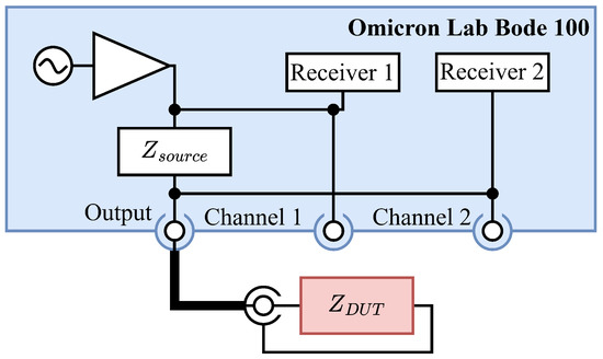
Figure 18.
One-port measurement method schematic.
As parameter was observed to be small, and within but near the limit of the one-port measurement method, a more accurate method was utilised in order to guarantee measurement accuracy. The shunt-thru measurement method was chosen to measure the total impedance of the PV modules modules in the region where the influence of was dominant [34]. This configuration, shown in Figure 19, emulates a Kelvin connection [34]. The RF source and amplifier applies a current through the DUT, and an independent receiver (connected to Channel 2) measures the voltage drop over the DUT. The resulting impedance of the DUT is determined from a 2-port S-parameter () measurement using Equation (16). The optimal measurement range of this method is from 0.5 mΩ to 100 Ω. For completeness, it should be noted that caution should be employed when attempting to use this method to measure inductances below 1 nH [34]. This measurement method can be susceptible to the effects of common-mode currents (induced within the loop formed between the Output and Channel 2 terminals). As a precautionary mitigation measure, clip-on ferrite beads were connected to all coaxial cabling.

Figure 19.
Shunt-thru measurement method schematic.
Since the values of parameters and are not influenced by the operating point of a PV cell, the source level was increased to the greatest level allowed by the VNA (without risking overload of the receivers). Even if large-signal operation of the PV cells were to occur, the values of the aforementioned would not have been affected. This practice of using high source levels resulted in an improved signal-to-noise ratio. These source levels, specified for a 50 Ω system, were 6 and , for the one-port and shunt-thru methods, respectively. The aforementioned measurement method allow for impedance measurements which are suitable for the extraction of small-signal AC parameters which do not change with the level of DC bias. The following subsection introduces a measurement method which allows for the analysis of small-signal AC parameters which do change with the level of DC bias.
4.1.2. With DC Bias
The capacitance of a PV cell junction varies with the operating point [29,35]. Therefore, a method of measuring the impedance of the PV modules at different levels of DC bias was required. Figure 20 shows a block diagram of a circuit, initially presented in [18], which allows for this type of measurement to be performed. This circuit, termed the Full Measurement Circuit, is made up of two sub-circuits—a Measurement Bridge and a DC Bias Tee. The Measurement Bridge, based off of the circuit in [36], serves the following two purposes: (1) it increases the measurable range of the VNA to multiple hundred kilo-ohms, and (2) it protects the Channel 1 (CH1) and Channel 2 (CH2) inputs of the Bode 100 from the potential application of a DC voltage resulting from an unintended exposure of the PV modules to solar irradiance [36]. The DC Bias Tee allows for the application of a DC voltage to the DUT without the risk of consequential DC current entering the Measurement Bridge, thereby further protecting the Bode 100. In the practical circuit, shown in Figure 21, a number of different possibilities for exist. These are selectable using different DIP (dual in-line package) switch combinations within the circuit. It is good practice to choose a sufficiently large value of , such that the impedance of the DUT is much lower than the impedance of within the intended measurement band—this minimises the possible influence of the DC Power Supply on the measured impedance. As with the unbiased small-signal AC measurements, an OSL calibration allows for the consideration of the layout and the parasitic elements of the Full Measurement Circuit by the VNA. For easy reproduction, Table 5 lists the values of the components employed in the Full Measurement Circuit.

Figure 20.
The measurement setup for small-signal AC impedance measurements with a DC bias. Developed from [18].

Figure 21.
A photograph of the constructed measurement circuit. The aluminium lid was replaced prior to commencement of the measurements. Developed from [18].
Table 5.
The values of the components employed in the Full Measurement Circuit. From [18].
When evaluating the impedance of a nonlinear device, one has to consider the trade-off between the test setup linearity and the signal-to-noise ratio. A low source level, which results in a low signal-to-noise ratio, provides greater surety that the nonlinear operation of the DUT will not be excited—at the risk of noisy measurement data. Conversely, a high source level, which results in a good signal-to-noise ratio, provides a stable and consistent measurement that is not corrupted by noise—at the risk of innacuracies resulting nonlinear operation where linearity is required. Therefore, choosing the correct source level is critical. The case of both the small and the large PV modules, the source level was able to be set as high as 13 without causing nonlinear operation. This was high enough to produce a good signal-to-noise ratio, but low enough not to cause nonlinear operation of the PV modules or saturation of the receivers within the Bode 100. Linearity was checked using a 100 MHz digital storage oscilloscope, connected in parallel with the measurement setup using a BNC T-Piece—no rectification effects were observed across the band. A separate OSL calibration was used for this linearity check. The oscilloscope was also removed, and another OSL calibration was performed, prior to the recording of any PV module impedance measurements.
Now that the measurement setups required for the small-signal AC parameters to be obtained have been described, the DC measurement setup is introduced.
4.2. Large-Signal DC Measurements
DC measurements were then performed, using the setup shown in Figure 22. This setup comprises: a DC voltage source, a digital storage oscilloscope, and a multimeter. Since all measurements were performed in a completely dark environment, the photocurrent, , was therefore set to zero in the LSDCSM. The DC voltage source was used to apply a voltage to each PV module. This voltage was recorded using the digital storage oscilloscope. The current provided by the DC voltage source was measured using the multimeter. The instruments employed were carefully chosen to ensure operation within the tolerances specified by their respective manufacturers. In this measurement setup, the DC voltage source is stepped through the desired range, whilst and are recorded simultaneously at each step. For the purposes of this article, the forward bias refers to the case where the voltage of the DC source, , is positive. For completeness, it is therefore stated that the reverse bias refers to the case where the voltage of the DC source, , is negative.
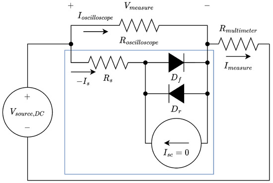
Figure 22.
DC measurement setup. The area in blue represents an instance of the LSDCSM. Developed from [18].
In this test setup, the influence of the oscilloscope is modelled by a resistance, —which was measured to be 1.195 MΩ. Ohm’s Law was used to calculate the current through the oscilloscope (i.e., ), and this current was subtracted from . Therefore, any remaining current, represented in Figure 22 as (-), had to have flowed through the PV modules. This compensation was particularly relevant when the reverse-bias operation of the PV modules were considered, as the current flowing through the oscilloscope was non-negligible.
Voltage was observed at the positive and negative terminals within the junction box of the PV modules. Therefore, the resistive effect of any wiring connected to these terminals was removed.
The combined resistance of the inter-cell wiring and contact resistances within the PV modules, , was also considered using Ohm’s Law—i.e., current (-) was multiplied by , and then subtracted from . What remained were current–voltage curves for the forward and reverse bias cases, to which Equation (1) could be fit, resulting in parameters for components and which were implementable in the default SPICE LSDM.
The forward bias operation of both PV modules was considered first. In this bias, the leakage current through component was assumed to be negligible. The voltage of the DC source was then slowly increased until the voltage per cell, following the aforementioned compensations, was equal to 0.6 V. Further voltage and current were available, however, the experiment was truncated so as to avoid too large an increase in the PV cell temperatures as a result of the dissipated power. This would have caused a noticeable change in the thermal voltage, , which would result in a divergence of the measured current–voltage curve from Equation (1). This divergence would not be compensable, since the SPICE solver considers the junction temperature in the LSDM to be constant within each simulation run.
The reverse bias operation of both PV modules were then considered. The DC source voltage was increased until enough data was gathered to enable Equation (1) to be fit to the post-compensation current–voltage curve. For the small PV module, this required a voltage of 0.975 V per cell. For the large PV module, this required a voltage of 4.2 V per cell—a total of 302.4 V for the full large PV module.
The extracted parameters for the forward and reverse bias cases are presented in Section 5.
5. Results
This section presents the results from the different test setups.
5.1. Small-Signal AC Results
The small-signal AC results are presented first. These were initially gathered using the unbiased test configuration. Then, the configuration which did apply a DC voltage bias was utilised. This allowed for the determination of parameters , , and .
5.1.1. Unbiased Small-Signal AC Results
The unbiased impedances of the two PV modules was first analysed using a one-port measurement method with the VNA, configured as follows: 801 logarithmically-spaced measurement points, a start frequency of 1 Hz, a stop frequency of 50 MHz, 0 dB of receiver attenuation on both receivers, and a receiver bandwidth of 30 Hz. A good balance between sweep time and measurement accuracy was achieved by this configuration. The Output terminal of the VNA was connected to the DUTs using a 30 cm BNC-BNC cable. This BNC-BNC cable then connected to the (aforementioned) BNC connectors, soldered between the output terminals (in the junction box) of each PV module.
An OSL calibration was performed prior to the commencement of the measurements, this compensated for the effects of parasitic and non-ideal elements within the measurement setup.
The base 10 logarithm of the magnitude of Equation (6) as the objective function for the curve_fit function. This enabled parameters for , , and (unbiased) to be extracted. As the magnitude of the measured impedance spanned multiple orders of magnitude, the sensitivity of the curve fitting procedure, without the base 10 logarithm, would have been negatively influenced by the largest magnitude values—which would have dominated the least squares sum. The use of the base 10 logarithm improved the outcome of the curve fitting procedure by reducing the dominance of large magnitude values, and increasing the influence of small magnitude values.
Even with the assistance of the base 10 logarithm, is still easily hidden within the overall magnitude data. Furthermore, the broad sweep utilised in the one-port measurements may have skipped over the frequency at which element is dominant. Therefore, the impedance measurements were repeated using the shunt-thru method for the segments of the frequency band where the influence of element was dominant. These measurements entailed a sweep of 801 linearly-spaced measurement points. Once the resonant point of each PV module had been identified in greater resolution, the recorded impedance was extracted at this point. Furthermore, in order to extract a more accurate value for , the value of the term (from Equation (6)) was calculated at the resonant point of each PV module. Then, the values produced by this calculation were subtracted from the real values of the impedance at the same resonant point. This resulted in the value for parameter for each PV module. The aforementioned parameters are listed on a per-cell basis in Table 6.
Table 6.
Per-cell small-signal AC parameters for the two PV modules.
Using the parameters from Table 6, an LTspice simulation was performed for each PV module (using the SSACSM circuit). The measured (one-port results) and simulated impedances for the small and large PV module are shown in Figure 23 and Figure 24, respectively. In general, good agreement, in both magnitude and phase, is demonstrated between the measured and simulated results. In these plots, the resonance between element and the parallel combination of elements and is clearly demonstrated. Element dominates the impedance below this frequency, and element dominates the impedance above this frequency.
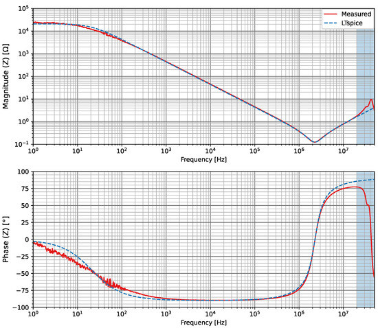
Figure 23.
Small PV module measured (one-port) and simulated per-cell impedance curves (frequency range 1 Hz to 50 MHz).

Figure 24.
Large PV module measured (one-port) and simulated per-cell impedance curves (frequency range 1 Hz to 50 MHz).
Figure 25 and Figure 26 show the measured (shunt-thru results) and simulated impedances of the small and large PV modules around their respective resonant points. Again, good agreement between the measured and simulated results is demonstrated. Over the displayed range, the Root-Mean-Square Error (RMSE) is 2.461 mΩ for the magnitude and 1.076° for the phase of the complex impedance of the small PV module. For the complex impedance of the large PV module over the same frequency range, the RMSE is 1.429 mΩ for the magnitude and 1.632° for the phase.
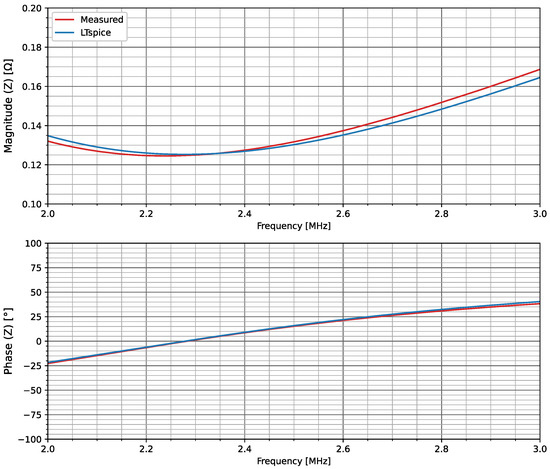
Figure 25.
Small PV module measured (shunt-thru) and simulated per-cell impedance curves (frequency range 2 MHz to 3 MHz).

Figure 26.
Large PV module measured (shunt-thru) and simulated per-cell impedance curves (frequency range 200 kHz to 300 kHz).
The frequency ranges covered by Figure 23 and Figure 24 demonstrate that the SSACSM is appropriate up to a particular frequency. One issue, however, with the SSACSM, is that with increasing frequency, one would expect the impedance of the PV module to increase ad infinitum. This is not the case as undesirable (i.e., parasitic and radiating elements) will begin to become more influential with increasing frequency.
For the small PV module, the influence of an undesirable element becomes noticeable above 20 MHz in the measured magnitude curve, however, the measured phase curve begins to diverge from the simulated phase curve as early as 3 MHz. At 40 MHz, a resonance occurs, and above this frequency an undesirable capacitance dominates the measured impedance. This causes a divergence from the impedance predicted by the SSACSM. Increasing the frequency further would undoubtedly uncover the influences of additional undesirable elements. For the region below 20 MHz (where the effects of undesirable elements are not yet dominant) in Figure 23, the RMSE is 15.76 Ω for the magnitude and 5.992° for the phase of the complex impedance of the small PV module.
Due to the increased complexity of the layout of the large PV module, the opportunity for an increased number of parasitic elements arises. Furthermore, due to the increased size of the large PV module (relative to the wavelengths of the frequencies involved), the likelihood of encountering radiating elements increases. For this PV module, the measured and simulated impedance magnitudes begin to disagree at approximately 1 MHz. The phases, again, begin to disagree earlier, at approximately 300 kHz. Multiple resonances are observed in the magnitude at and above 9 MHz, with corresponding changes also seen in the phase. As with the small PV module, the magnitude does not increase infinitely with frequency it is now bounded by the magnitudes of the peaks and troughs of the resonances between 9 MHz and 50 MHz. For the region below 1 MHz (where the effects of undesirable elements are not yet dominant) in Figure 24, the RMSE is 0.2270 Ω for the magnitude and 6.556° for the phase of the complex impedance of the large PV module.
The SSACSM could be amended with extra circuit elements, which could then be fit to the measured data in order to account for the effects of these undesirable elements. However, this process becomes especially challenging if sub-resonances (such as at 10 MHz in the magnitude plot for the large PV module) are to be considered. Future analyses, outside of the scope of this article, may wish to differentiate between parasitic, radiating, and mutually-coupled elements.
This section examined small-signal AC parameters of the small and large PV modules which do not change with the operating point. The following section examines the remaining small-signal AC parameter—which does change with the operating point.
5.2. DC Biased Small-Signal AC Results—Determining the Nonlinear Voltage-Dependent Capacitance
Biased measurements of the impedance of the small and large PV modules were performed using the following settings: 801 logarithmically-spaced frequency points, a start frequency of 100 , a stop frequency of 50 , 0 dB of attenuation on both receivers, and a receiver bandwidth of 30 Hz. The voltage of the DC source was varied in 1 V steps between 0 V and 35 V, with an impedance measurement being taken at each step.
This resulted in a set of 36 impedance measurements of both the small and large PV modules, which are shown in Figure 27 and Figure 28, respectively. These figures, which are presented on a per-cell basis (including the legends), show a 1 kHz–50 MHz sub-band of the impedance results. In these figures, one can clearly see the region in which the impedance of the PV cells is dominated by the capacitance of the cells themselves. For the small PV module, this region is shown in Figure 27 between 1 kHz and approximately 2.5 MHz. For the large PV module, this region is shown in Figure 28 between 1 kHz and 250 kHz. This dominant capacitance, and therefore the overall impedance, varies with the application of a bias voltage. As the magnitude of a reverse bias voltage is increased, the width of the depletion region increases—this decreases the capacitance of the PV cell junction, thereby increasing the impedance (for a constant frequency). As the impedance of the capacitance changes, the resonant point (at which the magnitude of the impedance is minimised) is shifted for each level of reverse bias.

Figure 27.
Small PV module measured per-cell impedance curves at multiple levels of reverse bias (frequency range 1 kHz to 50 MHz).
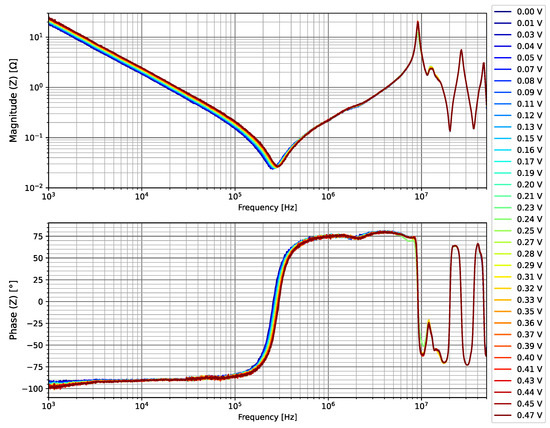
Figure 28.
Large PV module measured per-cell impedance curves at multiple levels of reverse bias (frequency range 1 kHz to 50 MHz).
As in Section 4.1.1, the effects of undesirable elements are prominent at higher frequencies. Figure 27 and Figure 28 show that the impedances of these elements do not change with reverse bias. Therefore, these figures further support the notion that these impedances are not wholly governed by the operation of the PV cells themselves, but rather the layout of the cells within the PV modules.
The impedances of the small and large PV modules were sampled at 18.336 kHz and 16.781 kHz, respectively. These represented frequencies at which the capacitances of each PV module were dominant (i.e., the measured phase was near ). Furthermore, the magnitude of impedances at these frequencies was near (i.e., within the same order of magnitude as) the resistance of the 50 Ω standard used in the OSL calibration—thus ensuring measurement accuracy. The resulting voltage–capacitance curves for the small and large PV modules are shown in Figure 29 and Figure 30, respectively. The RMSE for the fit capacitance over the displayed frequency range was for the small PV module and 0.0429 μF for the large PV module. Note that these figures are presented on a per-cell basis, and that the voltage axis in these curves has been corrected for the voltage drop over component in the measurement setup.
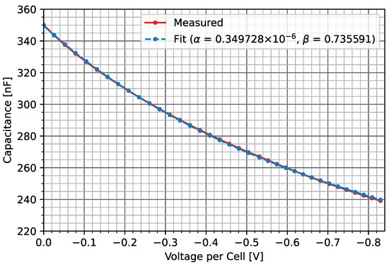
Figure 29.
Small PV module measured and fit per-cell capacitance curves at multiple levels of reverse bias.

Figure 30.
Large PV module measured and fit per-cell capacitance curves at multiple levels of reverse bias.
As a mathematical expression for the capacitance–voltage relationship was required for implementation in LTspice, Equation (17) was fit to the measured capacitance–voltage curve. The shape of the curve produced by Equation (17) is governed by two constants: and . The constants resulting from the curve fitting procedure are presented for each PV module in Table 7.
Table 7.
Capacitance modelling parameters for the two PV modules.
As Figure 29 and Figure 30 present measured capacitance–voltage measurements obtained using a small-signal based method, this measurement data represents a local capacitance—referred to as in Section 3.3.1. Following this, again as per Section 3.3.1, it is necessary to apply Equation (14) to Equation (17), thereby producing Equation (18). Equation (18), therefore, represents a total capacitance—referred to as in Section 3.3.1. It is this total capacitance which allows the model to accurately handle both large-signal and small-signal stimuli. Thus, the controlling equation for the dependent voltage source, represented C_Rep in Figure 15, was set to Equation (17).
Following this, the voltage-dependent capacitance was constructed in LTspice using the method described previously (in Section 3.3.1).
At this point, the only remaining parameters required for the FCPVM were those that governed DC operation. These are covered in the following section.
5.3. Large-Signal DC Results
In the large-signal DC current–voltage measurements, the terminals of the voltage probe were connected to the input and output terminals of the junction box of each PV module. This removed the possibility of any influence from the wires, typically supplied with a PV module, connected to these terminals. Ohm’s Law was used in each case to compensate for the effect of the oscilloscope input resistance, as well as the the influence of component (measured in Section 5.1.1), before curve fitting was applied. As the measured data spanned multiple orders of magnitude, the natural logarithm of Equation (1) was used as the objective function for in all DC curve fitting cases—this assisted the curve-fitting procedure. The natural logarithm of the corresponding measurement data was also therefore used as the input data. The thermal voltage, , was calculated according to the parameters listed previously in Table 2. As low power levels were employed, the PV cell temperatures, T, were assumed to be equal to the ambient temperature—which was set to the same as the temperature as in Table 2 by means of a climate control system. Parameter was set to zero in the curve fitting procedure, as it only exists to assist convergence within the SPICE solver.
5.3.1. Forward Bias Results
In the forward bias case, the voltage of the DC source was increased until the current–voltage curve exhibited the standard "knee" diode turn-on characteristic. This is shown for the small and large PV module on a per-cell basis in Figure 31 and Figure 32, respectively. The parameters resulting from the forward-bias curve fitting procedure are presented in Table 8. These parameters were then applied to the FCPVM, and a DC-sweep of the model was performed in LTspice. The recorded simulation output is also presented in the aforementioned figures. In general, the measured and simulated results show good agreement, particularly between 0.5 V and 0.6 V. Above 0.58 V for the small PV module, and 0.55 V for the large PV module, the current–voltage plot exhibits a linear trend, as the effect of element begins to become dominant. The overall forward bias RMSE over the displayed voltage range is for the small PV module and for the large PV module. As mentioned earlier, higher currents were not tested as these would result in an increase in the PV cell temperatures, resulting in a change in the thermal voltage, which SPICE does not recalculate within a simulation run.

Figure 31.
Small PV module measured and simulated current–voltage relationship for positive DC voltages.
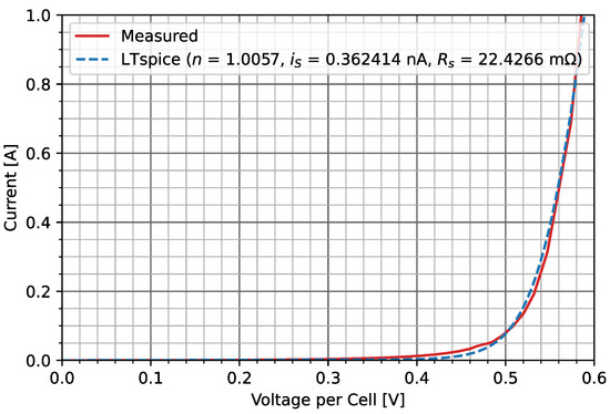
Figure 32.
Large PV module measured and simulated current–voltage relationship for positive DC voltages.
Table 8.
Forward bias () large-signal DC parameters for the two PV modules.
5.3.2. Reverse Bias Results
In the reverse bias case, DC source voltage was increased until a weak exponential current–voltage relationship was exhibited. This is shown in Figure 33 and Figure 34 for the small and large PV modules, respectively. The small PV module exhibited this trend with a smaller per cell voltage range than the large PV module. This provided sufficient information for the aforementioned natural logarithm-based curve fitting procedure. Prior to curve fitting, the effect of the oscilloscope, element , and the reverse leakage current through element were compensated for. The reverse leakage current through element occurs as a pre-breakdown current in the default SPICE LSDM, specified previously as − for this element in Table 8. Table 9 presents the results from the reverse bias curve fitting procedure.
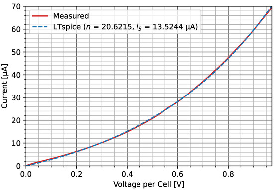
Figure 33.
Small PV module measured and simulated current–voltage relationship for negative DC voltages.
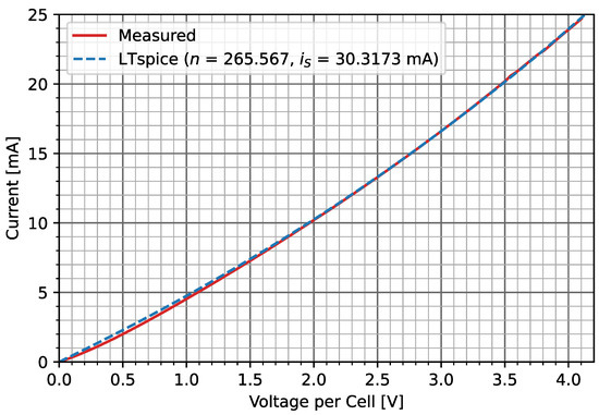
Figure 34.
Large PV module measured and simulated current–voltage relationship for negative DC voltages.
Table 9.
Reverse bias () DC large-signal parameters for the two PV modules.
As before, the parameters extracted from the curve fitting procedure were applied to the FCPVM, and a DC-sweep of the model was performed in LTspice. The recorded simulation output is also presented in the aforementioned figures.
Figure 33 and Figure 34 both show good agreement between the measured and simulated results. In both cases, a slight disagreement between the measured and simulated results did occur within the lower 20% of the measured voltage range. However, these disagreements are considered negligible for the large-signal intended uses of the FCPVM. In each case, as these results exhibit a nonlinear current–voltage relationship in reverse bias, they present an improvement on the general practice of using a resistive component to model reverse bias operation. The overall reverse bias RMSE over the displayed voltage range is 0.2595 μA for the small PV module and for the large PV module.
For completeness, a parallel combination of a resistive and diode element was assessed for its ability to model reverse bias operation. This approach was successfully demonstrated in [18] for modelling the reverse bias operation of Schottky diodes. However, the configuration proposed by the the FCPVM exhibited superior accuracy.
All the necessary parameters for the FCPVM have now been determined. The accuracy of the small-signal AC parameters have been demonstrated using frequency-domain AC simulations. The accuracy of the DC parameters have been demonstrated using DC sweep simulations. The following section demonstrates the working of the full model under both small-signal AC operation and large-signal transient operation.
6. Full Model Demonstrations
The FCPVM was implemented in LTspice, as per Figure 15. In this section, its operation is demonstrated in the time domain using the following two types of stimuli: (1) small-signal continuous waveform (CW), and (2) large-signal transient. The parameters for a single cell from the small PV module were used in this demonstration. The photocurrent was set to zero for these demonstrations.
6.1. Small-Signal Continuous Waveform
To show the ability of the FCPVM to handle small-signal AC CW stimuli, it was connected to a voltage source producing a sinusoidal 1 mVpeak signal. Two cases were simulated for, one at a low frequency (10 kHz), and one at a high frequency (20 MHz).
The low frequency case is considered first. This case utilises a frequency which corresponds with a region in which the capacitance of the PV cell should dominate the overall impedance, as per the small-signal AC impedance plot shown previously in Figure 23 in Section 4.1.1. For this case, the voltage over and the current through the PV cell is shown in the time domain in Figure 35. As expected for a small-signal stimuli, the simulated current reaches equal magnitudes in forward and reverse bias. Furthermore, the simulated voltage lags the current by +91.0. The magnitude of the current reaches an amplitude of 21.974 μA. In phasor form, this results in an impedance of , which corresponds well with the measured impedance at this frequency in Figure 23.
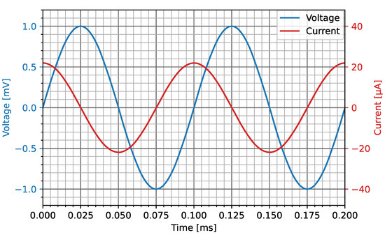
Figure 35.
Simulated voltage and current curves (1 mV, 10 kHz input signal applied).
The high frequency case is then considered. This case utilises a frequency which corresponds with a region in which the inductance should dominate the overall impedance, as per the aforementioned small-signal AC impedance plot.
For this case, the voltage over and the current through the PV cell is shown in the time domain in Figure 36. Again, as expected for a small-signal stimuli, the simulated current reaches equal magnitudes in forward and reverse bias. The voltage now leads the current by +86.4, and the magnitude of the current reaches an amplitude of 602.19 μA. In phasor form, this corresponds to an impedance of , which aligns well with the small-signal AC simulated impedance at this frequency in Figure 23. Note that the small-signal AC simulated impedance, and not the measured impedance, in Figure 23 is referred to in this case. This is because at this frequency the phase of the measured impedance has already begun to diverge from the model-predicted phase due to the influence of undesirable elements—which are considered to be outside of the scope of this article. Nevertheless, good agreement between the intended and implemented model has now been demonstrated for the small-signal case.
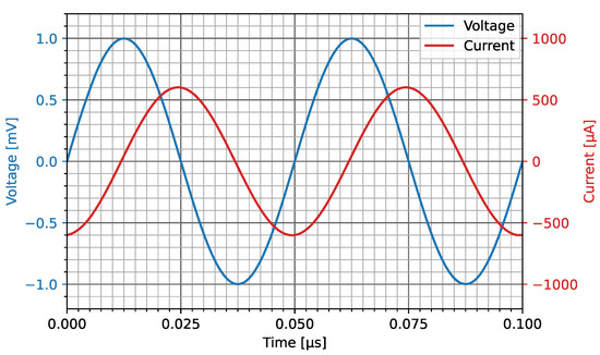
Figure 36.
Simulated voltage and current curves (1 mV, 20 MHz input signal applied).
6.2. Large-Signal Transient
To show the behaviour of the FCPVM to large-signal transient stimuli, a pulse generator circuit was constructed in LTspice. This circuit, initially presented in [18], and similar to the constructed setup in [12], is shown in Figure 37. Transient simulations were performed with the FCPVM connected (separately) in both the forward and reverses biases.

Figure 37.
The pulse generating circuit used to demonstrate large-signal transient operation of the FCPVM. Developed from [18].
In this simulation, capacitor C1 was charged to an initial voltage of 5 V. Switch S1 closes 100 μs after the simulation begins. Resistor R4 represents the equivalent series resistance of capacitor C1. Resistors R1, R2, and R3, and inductor L1, represents a pulse-shaping network, which modifies the quasi-step voltage input at the output of switch S1. Parameters for the small PV module, on a per-cell basis, were used in these simulations.
The simulated voltage over and current through the forward biased full circuit PV module are shown in Figure 38. As anticipated, the model quickly becomes forward biased. A large forward current and a small voltage drop are observed.

Figure 38.
Simulated voltage and current curves (large-signal transient stimulus, applied in the forward bias).
The model was then connected in the reverse bias and the simulation was rerun, producing the current and voltage curves shown in Figure 39. As expected, a sharp voltage rise is initially experienced, and little reverse current flows throughout the duration of the simulation. Noteworthy is the small, initial spike in current—representing current that charges up the capacitance of the PV cell.

Figure 39.
Simulated voltage and current curves (large-signal transient stimulus, applied in the reverse bias).
Identical vertical axes were purposely used to represent results for the forward and reverse biased cases. This clearly demonstrates that the constructed model behaves differently as a result of the applied bias. If a linearised model were to be used for this purpose, such as in [8], then the forward and reverse bias cases would produce respective voltage and current waveforms which would be indistinguishable from each other—i.e., a gross oversimplification of current–voltage characteristics of a device that exhibits certain nonlinear behaviour. Therefore, it is critical that the correct model be utilised given the context of a particular simulation.
7. Discussion
A novel full circuit PV model (FCPVM) was proposed in this article. As outlined in Section 2 and Section 3, this model overcomes limitations of previous DC-only or small-signal AC-only circuit models, which were limited to their respective domains. The implemented model allows for large-signal DC, small-signal AC, large-signal AC, and transient conditions to be considered—separately or together in a time-domain analysis. This was demonstrated in Section 6.
The presented model utilises standard components within the freely-available SPICE simulator, allowing researchers to implement it without requiring the purchase of any software licences. Furthermore, the SPICE-based implementation allows for it to be implemented in CEM simulations of PV installations—thereby combining the circuit and electromagnetic domains.
The specific novel contributions of this article are elaborated on below.
Novel Contribution 1: The presented model improved on the reverse-bias behaviour of the default SPICE LSDM by the addition of a secondary diode component, placed in parallel (with opposing polarity) with the original diode component. Furthermore, this secondary diode component effectively replaced the parallel resistance, , usually included in the SDM—enabling nonlinear reverse-bias current–voltage behaviour. The resulting implementation showed good agreement between the measured and simulated results, particularly at large reverse-bias voltages—a region of interest in studies involving the simulation of surges within PV installations. This method is explained in Section 3 and demonstrated in Section 5.3.
Novel Contribution 2: In Section 3.3.1 and Section 5.2, the presented model explains and demonstrates (respectively) the correct SPICE implementation of a voltage–dependent capacitance within the context of PV-focussed simulations. This implementation, which utilises a total capacitance instead of a local capacitance, is critical to allow for the model to be used for both small and large-signal perturbations.
Novel Contribution 3: Parameters for both a small and a large PV module are presented in Section 5—allowing researchers to choose parameters which are most appropriate for their particular application. Parameters are presented on a per-cell basis, allowing them to be easily adjusted to apply to PV modules which do not include the same number of cells as the assessed modules. These parameters were based on the observed characteristics of two real PV modules, rather than analytically-focussed predictions. In all cases, these parameters were obtained from measurements which were carefully performed using appropriate hardware—as explained in Section 4. Parameters relevant to modelling dynamic conditions were obtained using a VNA in multiple measurement configurations: one-port (for accurate general broad-band impedance measurements), shunt-thru (for accurate low impedance measurements), and a combination of a measurement bridge and a DC bias tee (for impedance measurements at multiple operating points). These measurements all exhibited excellent dynamic range, and the number of measurement points employed overcame the possibility of incorrect or over-extrapolated data—which other measurement methods (such as with a signal-generator and oscilloscope) are prone to. Moreover, the VNA provided phase information in addition to magnitude information, allowing for a straightforward comparison between the measured and simulated results across the band. The VNA-based measurements employed an OSL calibration procedure, which ensured accurate results.
Novel Contribution 4: Parameters relating to DC operation were obtained after compensating for the parasitic effects of the test setup—such as the input resistance of the oscilloscope—or the voltage drop over resistance in the FCPVM. This was crucial step to ensure accurate results, and is covered in Section 4.2.
Novel Contribution 5: The VNA measurements uncovered the effects of undesirable elements within the PV modules at higher frequencies. These effects, which are demonstrated in Section 5.1.1, are due to the presence of parasitic elements, mutual coupling, and radiating elements within the PV modules. The presence of these elements inhibits the magnitude of the impedance of the PV modules from increasing with frequency ad infinitum—as standard models would suggest. Although outside of the scope of this article, these elements need to be considered in PV-focussed modelling in the MHz range, and above.
Author Contributions
Conceptualization, K.M.C.; methodology, K.M.C.; software, K.M.C.; validation, K.M.C.; formal analysis, K.M.C.; investigation, K.M.C.; resources, K.M.C., P.G.W. and A.J.R.; data curation, K.M.C.; writing—original draft preparation, K.M.C.; writing—review and editing, P.G.W. and A.J.R.; visualization, K.M.C.; supervision, P.G.W. and A.J.R.; project administration, P.G.W. and A.J.R.; funding acquisition, P.G.W. and A.J.R. All authors have read and agreed to the published version of the manuscript.
Funding
This research received no external funding.
Institutional Review Board Statement
Not applicable.
Informed Consent Statement
Not applicable.
Data Availability Statement
Data used in this study are available upon request to the corresponding author.
Acknowledgments
The authors would like to thank the Cape Peninsula University of Technology (CPUT) for the use of the OMICRON Lab Bode 100.
Conflicts of Interest
The authors declare no conflict of interest.
References
- Sadiku, M. Electromagnetic compatibility. IEEE Potentials 1992, 11, 16–18. [Google Scholar] [CrossRef]
- Smit, H. Investigating Surge Protection and Earthing Designs Used for Utility-Scale PV Plants. Master’s Thesis, Stellenbosch University, Stellenbosch, South Africa, 2021. [Google Scholar]
- Coetzer, K.M.; Wiid, P.G.; Rix, A.J. The MOV as a Possible Protection Measure for Bypass Diodes in Solar PV Modules. In Proceedings of the 2019 International Conference on Clean Electrical Power (ICCEP), Otranto, Italy, 2–4 July 2019; pp. 286–291. [Google Scholar] [CrossRef]
- International Electrotechnical Commission. Photovoltaic Power Generating Systems—EMC Requirements and Test Methods for Power Conversion Equipment; International Electrotechnical Commission: Geneva, Switzerland, 2021. [Google Scholar]
- Wilson, C.; Storey, M.; Tzioumis, T. Protection and self-protection of the Murchison Radio-astronomy Observatory from radio frequency interference. In Proceedings of the 2011 XXXth URSI General Assembly and Scientific Symposium, Istanbul, Turkey, 13–20 August 2011; pp. 1–3. [Google Scholar] [CrossRef]
- Haeberlin, H.; Minkner, R. A simple method for lightning protection of PV-systems. In Proceedings of the 12th European Solar Energy Conference and Exhibition, Amsterdam, The Netherlands, 11–15 April 1994. [Google Scholar]
- Haeberlin, H. Interference Voltages induced by Magnetic Fields of Simulated Lightning Currents in Photovoltaic Modules and Arrays. In Proceedings of the 17th European Photovoltaic Solar Energy Conference, Munich, Germany, 22–26 October 2001. [Google Scholar]
- Formisano, A.; Hernández, J.C.; Petrarca, C.; Sanchez-Sutil, F. Modeling of PV Module and DC/DC Converter Assembly for the Analysis of Induced Transient Response Due to Nearby Lightning Strike. Electronics 2021, 10, 120. [Google Scholar] [CrossRef]
- Zhang, Y.; Chen, H.; Du, Y. Transients in solar photovoltaic systems during lightning strikes to a transmission line. Int. J. Electr. Power Energy Syst. 2022, 134, 106885. [Google Scholar] [CrossRef]
- Coetzer, K.M.; Wiid, P.G.; Rix, A.J. Investigating Lightning Induced Currents in Photovoltaic Modules. In Proceedings of the 2019 International Symposium on Electromagnetic Compatibility—EMC EUROPE, Barcelona, Spain, 2–6 September 2019; pp. 261–266. [Google Scholar] [CrossRef]
- Coetzer, K.M.; Wiid, P.G.; Rix, A.J. PV Installation Design Influencing the Risk of Induced Currents from Nearby Lightning Strikes. In Proceedings of the 2019 International Conference on Clean Electrical Power (ICCEP), Otranto, Italy, 2–4 July 2019; pp. 204–213. [Google Scholar] [CrossRef]
- Coetzer, K.M. Investigating PV Module Failure Mechanisms Caused by Indirect Lightning Strikes. Master’s Thesis, Stellenbosch University, Stellenbosch, South Africa, 2019. [Google Scholar]
- 3DS CST Studio Suite. Available online: https://www.3ds.com/products-services/simulia/products/cst-studio-suite/ (accessed on 15 October 2022).
- Masters, G.M. Renewable and Efficient Electric Power Systems, 2nd ed.; Wiley-Interscience: Hoboken, NJ, USA, 2004; pp. 445–446. [Google Scholar]
- Jordehi, A.R. Parameter estimation of solar photovoltaic (PV) cells: A review. Renew. Sustain. Energy Rev. 2016, 61, 354–371. [Google Scholar] [CrossRef]
- Villalva, M.G.; Gazoli, J.R.; Filho, E.R. Comprehensive Approach to Modeling and Simulation of Photovoltaic Arrays. IEEE Trans. Power Electron. 2009, 24, 1198–1208. [Google Scholar] [CrossRef]
- da Luz, C.M.A.; Tofoli, F.L.; dos Santos Vicente, P.; Vicente, E.M. Assessment of the ideality factor on the performance of photovoltaic modules. Energy Convers. Manag. 2018, 167, 63–69. [Google Scholar] [CrossRef]
- Coetzer, K.M.; Rix, A.J.; Wiid, P.G. The Measurement and SPICE Modelling of Schottky Barrier Diodes Appropriate for Use as Bypass Diodes within Photovoltaic Modules. Energies 2022, 15, 4783. [Google Scholar] [CrossRef]
- Alrahim Shannan, N.M.A.; Yahaya, N.Z.; Singh, B. Single-diode model and two-diode model of PV modules: A comparison. In Proceedings of the 2013 IEEE International Conference on Control System, Computing and Engineering, Penang, Malaysia, 29 November–1 December 2013; pp. 210–214. [Google Scholar] [CrossRef]
- Babu, B.C.; Gurjar, S. A Novel Simplified Two-Diode Model of Photovoltaic (PV) Module. IEEE J. Photovoltaics 2014, 4, 1156–1161. [Google Scholar] [CrossRef]
- Kim, K.A.; Xu, C.; Jin, L.; Krein, P.T. A Dynamic Photovoltaic Model Incorporating Capacitive and Reverse-Bias Characteristics. IEEE J. Photovoltaics 2013, 3, 1334–1341. [Google Scholar] [CrossRef]
- Prajapati, M. Modeling and Analysis of EMI from DC Input of Photovoltaic Systems. Ph.D. Thesis, Nanyang Technological University, Singapore, 2019. [Google Scholar] [CrossRef]
- MATLAB—MathWorks—MATLAB & Simulink. 2020. Available online: https://www.mathworks.com/products/matlab.html (accessed on 28 July 2022).
- BYD Company. BYD P6C-36 Series-3BB. 2013. Available online: https://cdn.enfsolar.com/Product/pdf/Crystalline/54c7444bee304.pdf (accessed on 28 September 2022).
- ACDC Dynamics. Product Specification Sheet: SLP005-12. Available online: http://a365.acdc.co.za/Images//spec/SLP005-12.pdf (accessed on 28 July 2022).
- Roehr, W.D. Rectifier Applications Handbook (Motorola); Motorola, Inc.: Holtsville, NY, USA, 1993; Chapter 3; pp. 49–87. [Google Scholar]
- Python. Available online: https://www.python.org/ (accessed on 16 May 2022).
- Matplotlib: Visualization with Python. Available online: https://matplotlib.org/ (accessed on 16 May 2022).
- Neamen, D.A. Semiconductor Physics and Devices, 4th ed.; McGraw-Hill: New York, NY, USA, 2012; pp. 334–336. [Google Scholar]
- Zeltser, I.; Ben-Yaakov, S. On SPICE simulation of voltage-dependent capacitors. IEEE Trans. Power Electron. 2018, 33, 3703–3710. [Google Scholar] [CrossRef]
- LTspice Simulator. 2021. Available online: https://www.analog.com/en/design-center/design-tools-and-calculators/ltspice-simulator.html (accessed on 2 October 2022).
- Scipy. Available online: https://www.scipy.org/ (accessed on 1 October 2021).
- OMICRON Lab. Bode 100 User Manual ENU1006 05 03. 2017. Available online: https://www.omicron-lab.com/fileadmin/assets/Bode_100/Manuals/Bode-100-User-Manual-ENU10060503.pdf (accessed on 1 October 2022).
- OMICRON Lab. Bode 100 Application Note—Impedance Measurements Using the Bode 100 V1.0. 2020. Available online: https://www.omicron-lab.com/fileadmin/assets/Bode_100/ApplicationNotes/Impedance_Measurement_methods_using_the_Bode_100/2020-10-21_Bode_Appnote_Impedance_Measurements_V1_0.pdf (accessed on 14 September 2022).
- Hu, C. Modern Semiconductor Devices for Integrated Circuits; Prentice Hall: Upper Saddle River, NJ, USA, 2010. [Google Scholar]
- Hämmerle, F. Bode 100 Application Note—Solar Cell Impedance Measurement V2.0. 2017. Available online: https://www.omicron-lab.com/fileadmin/assets/Bode_100/ApplicationNotes/SolarCell/App_Note_Solar_Impedance_V2_0.pdf (accessed on 24 September 2022).
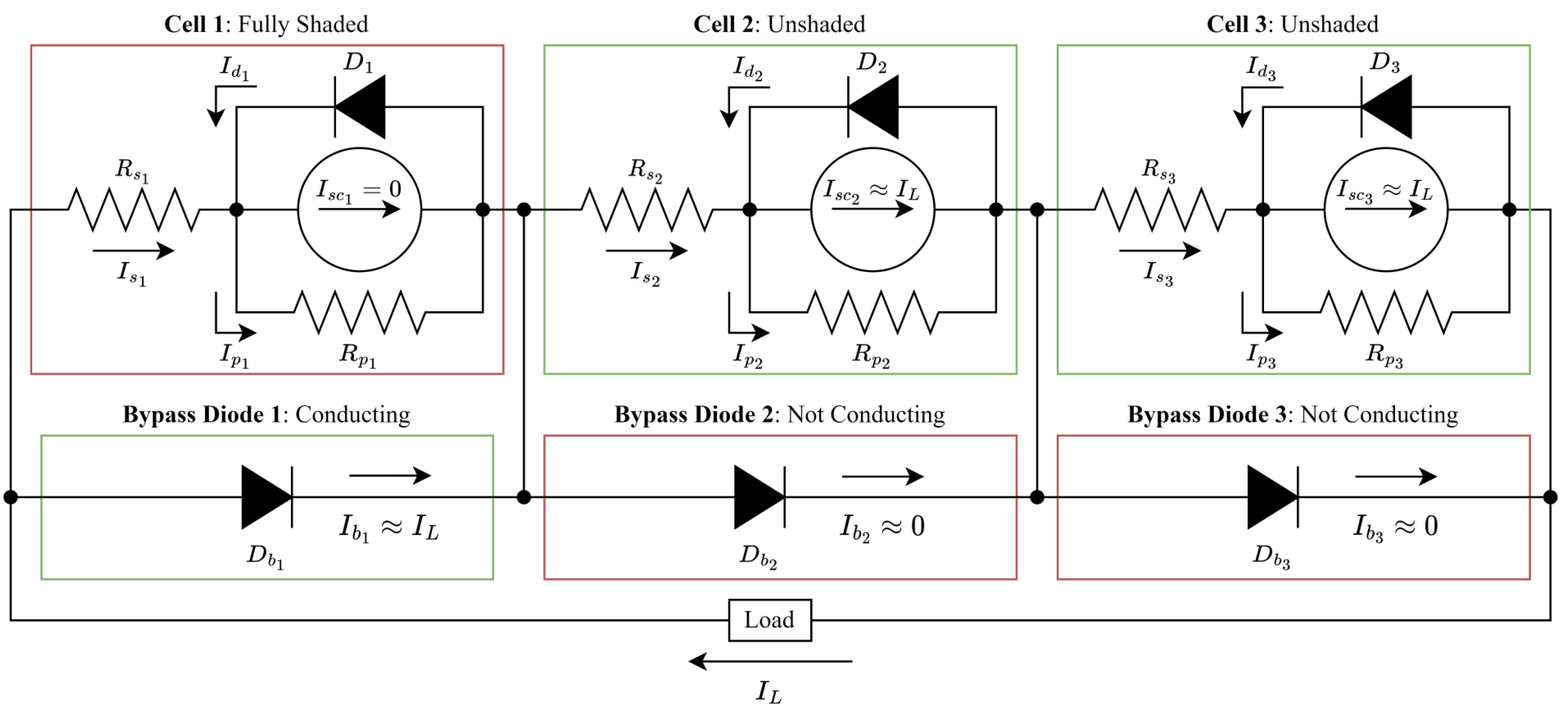
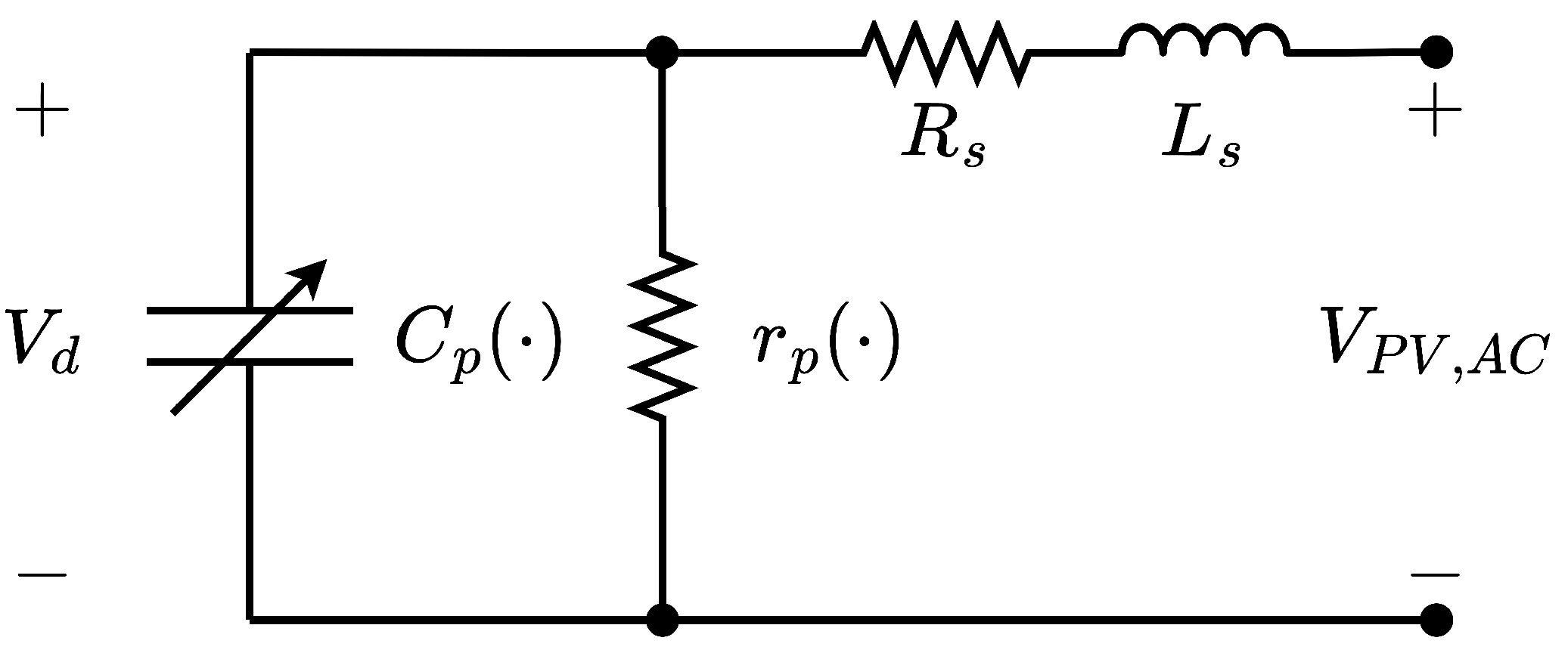
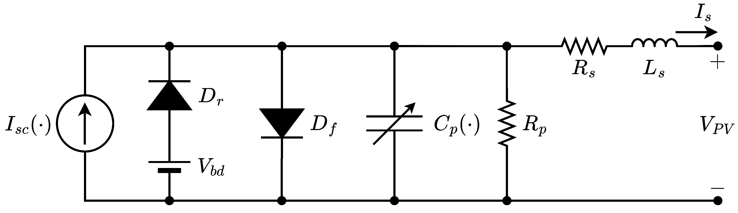
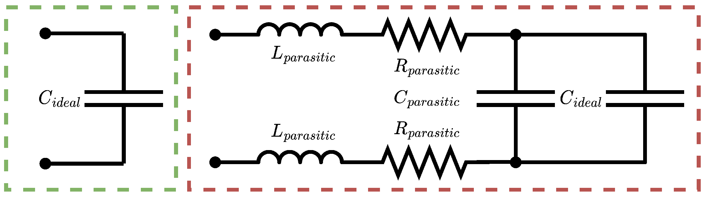

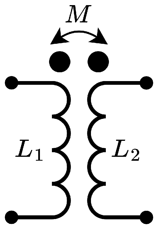
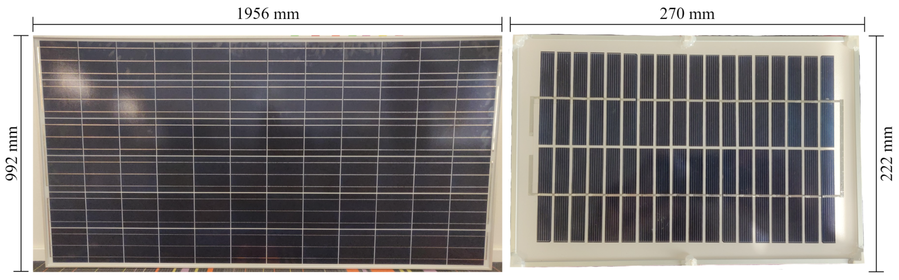

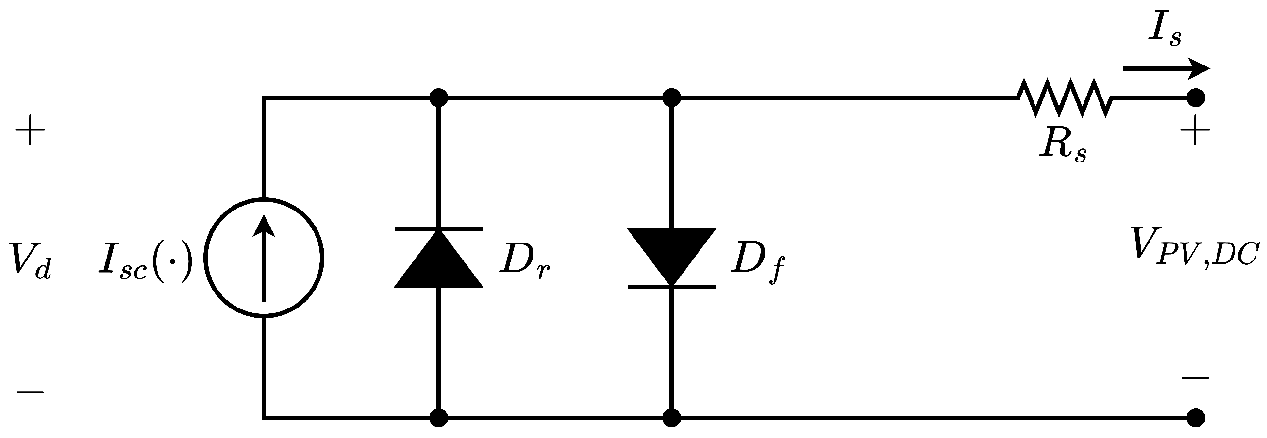
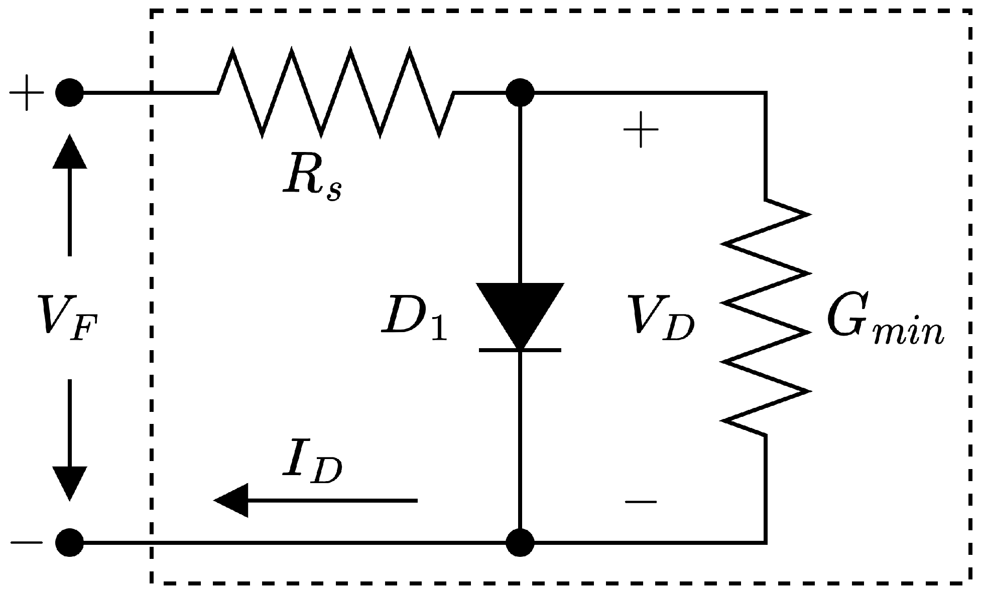
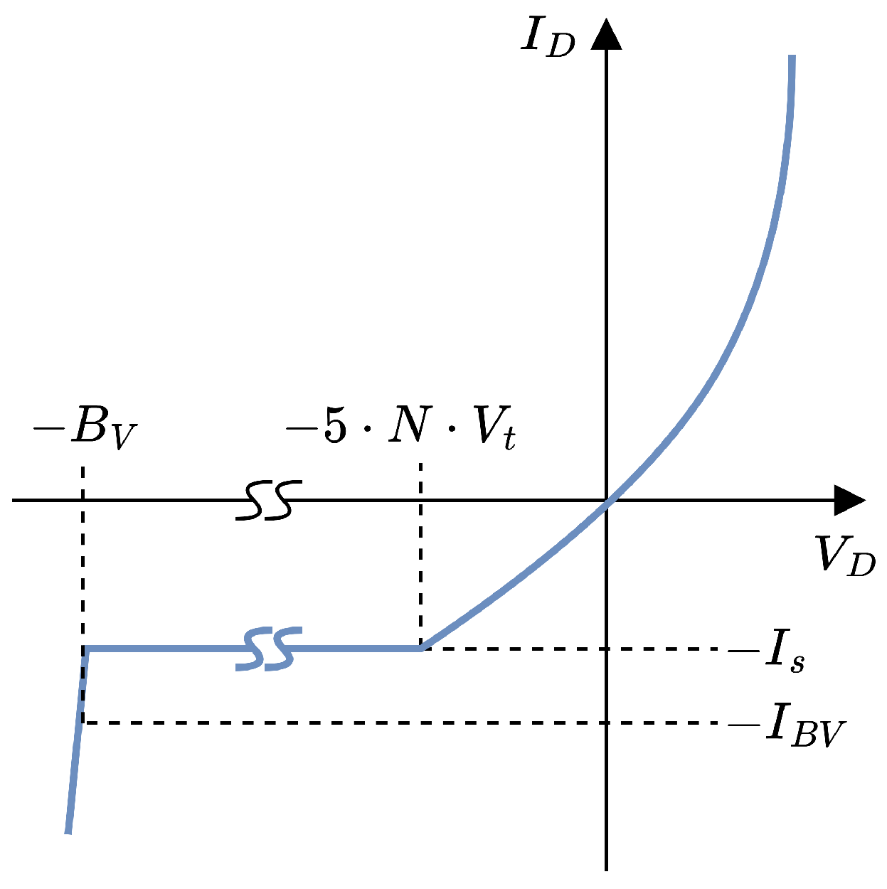
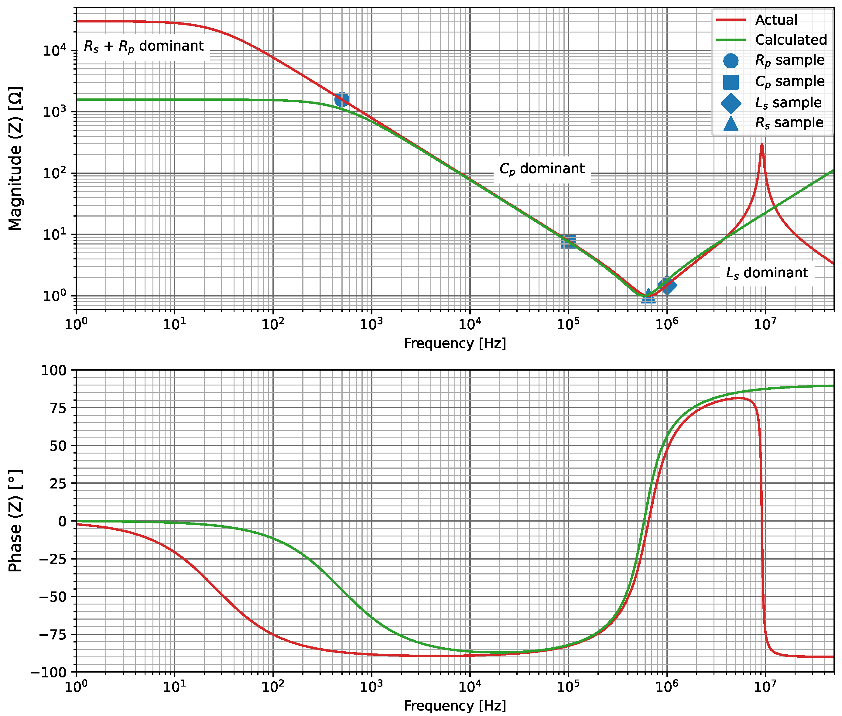
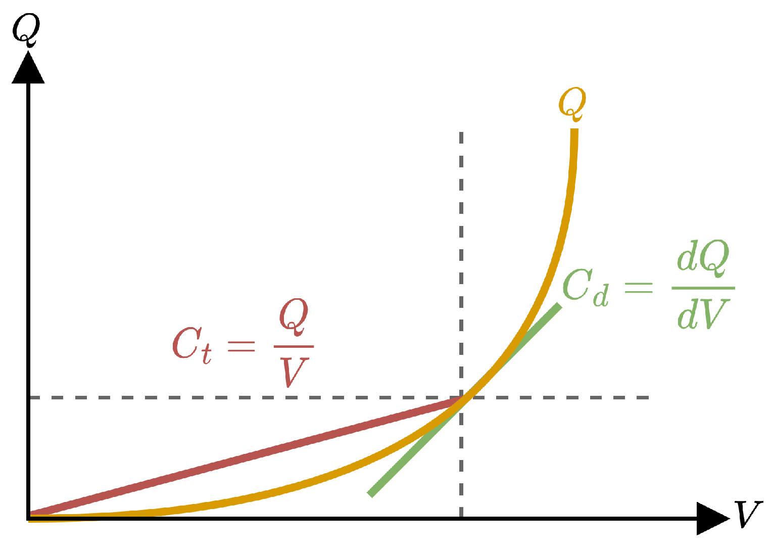
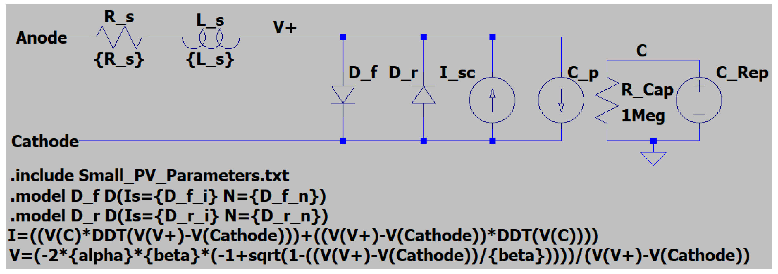
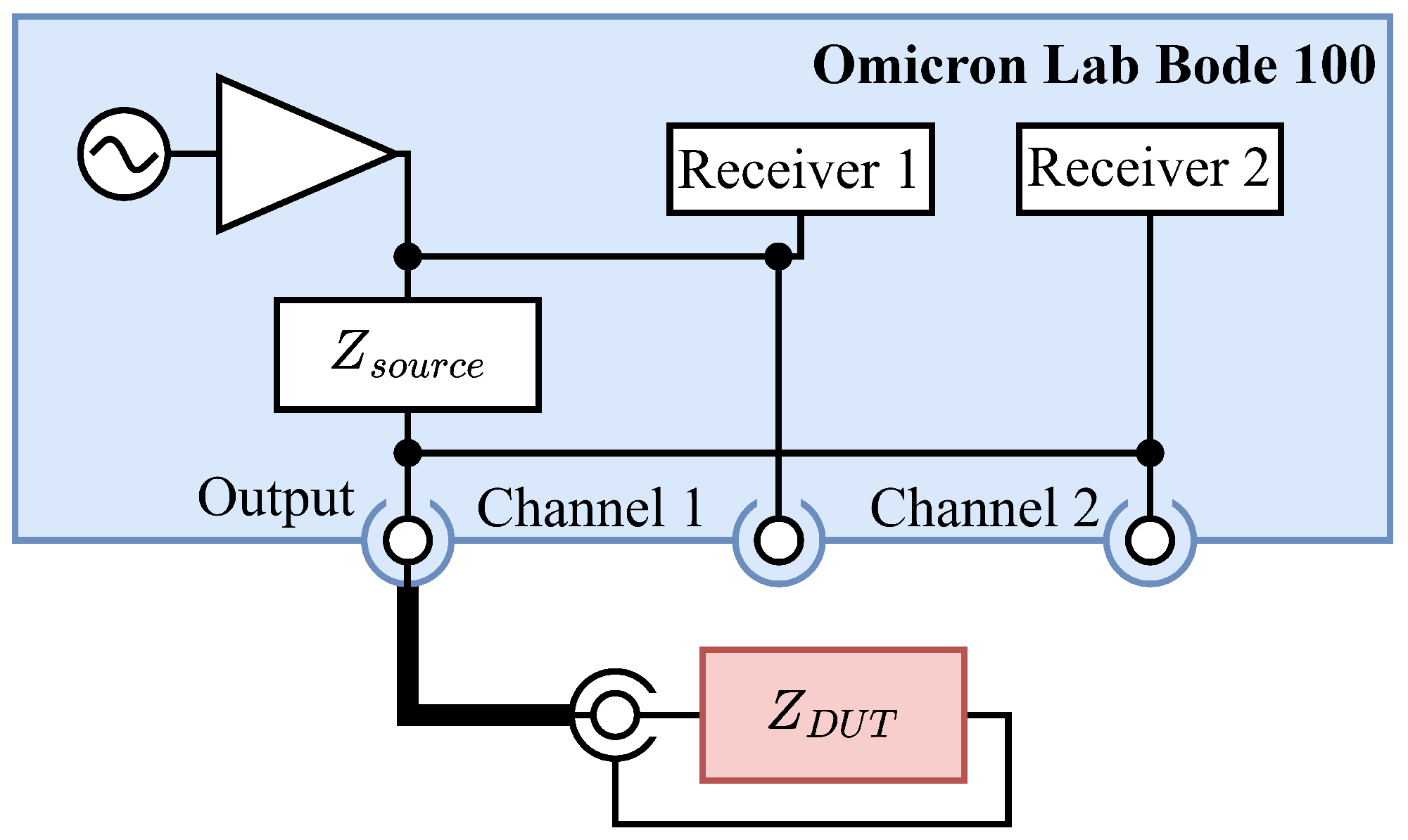
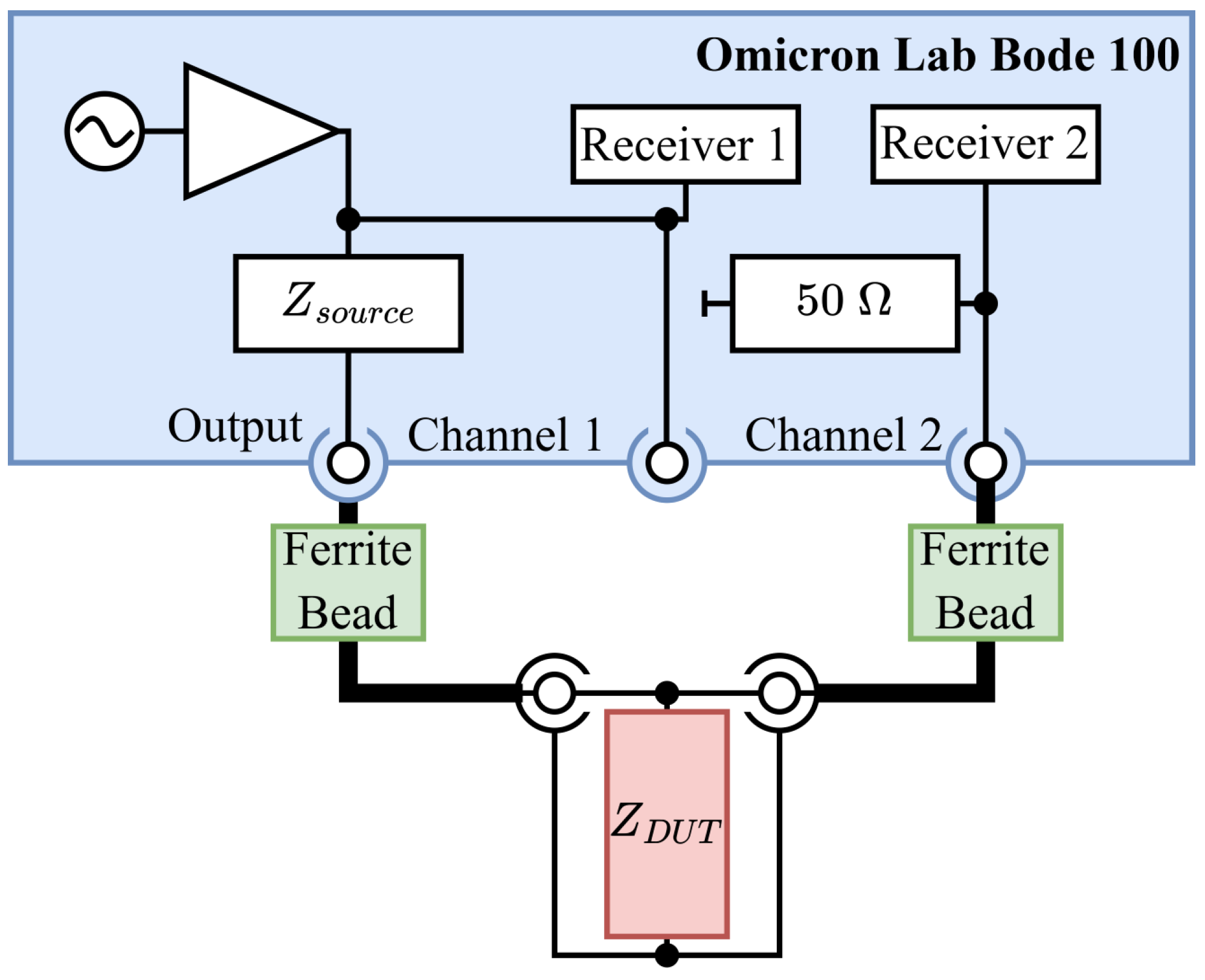
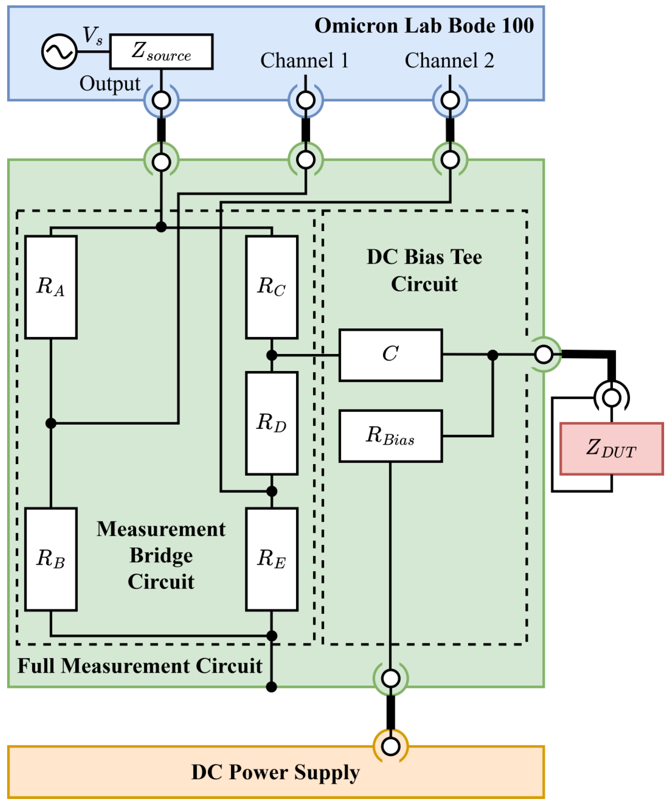
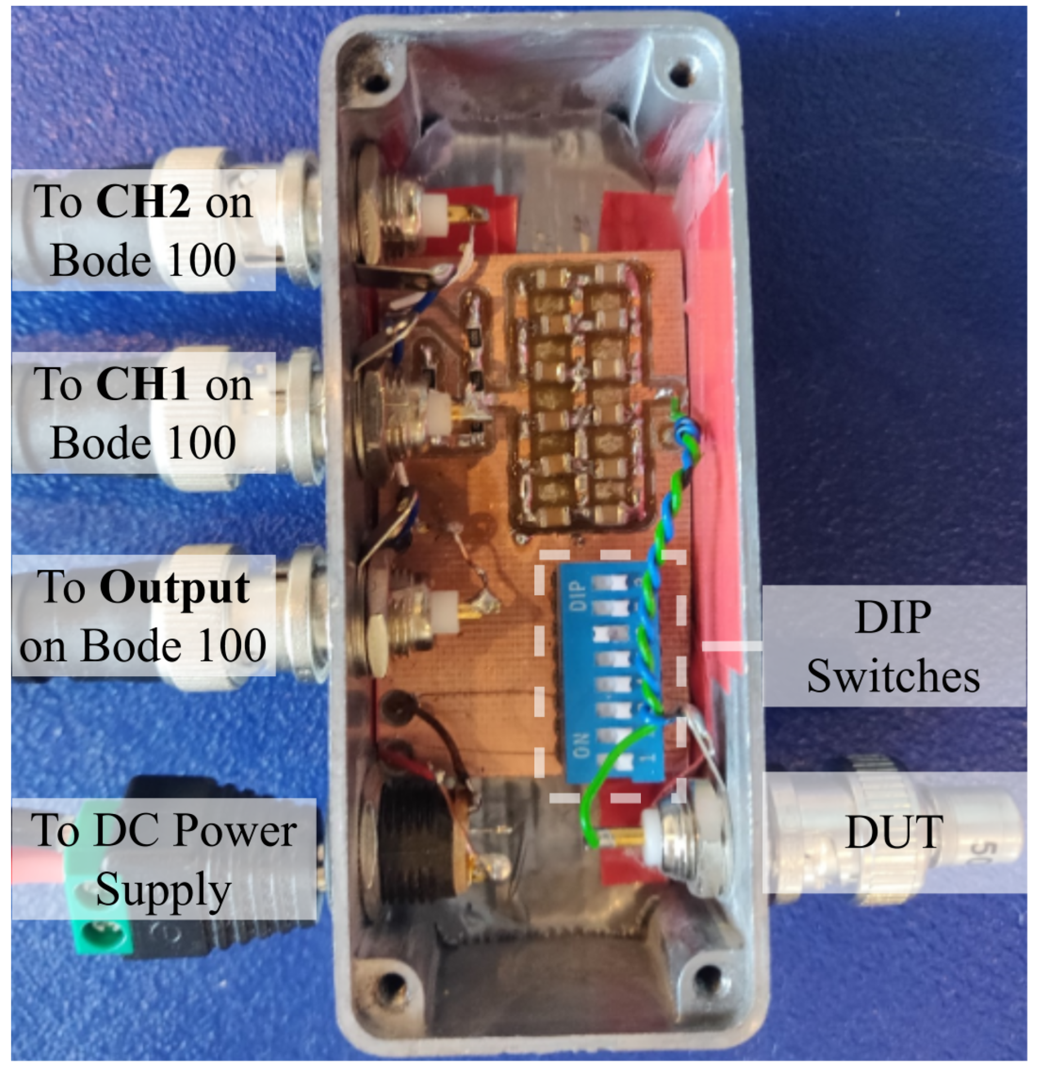
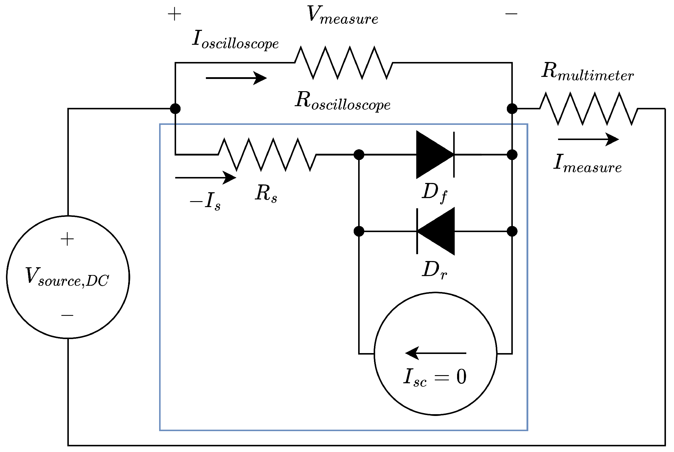
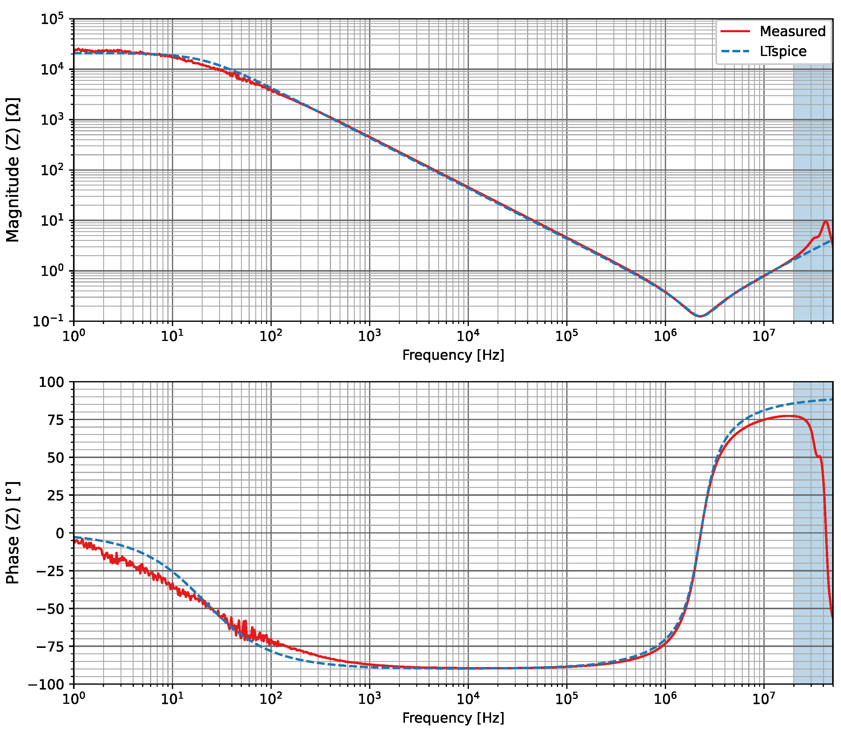
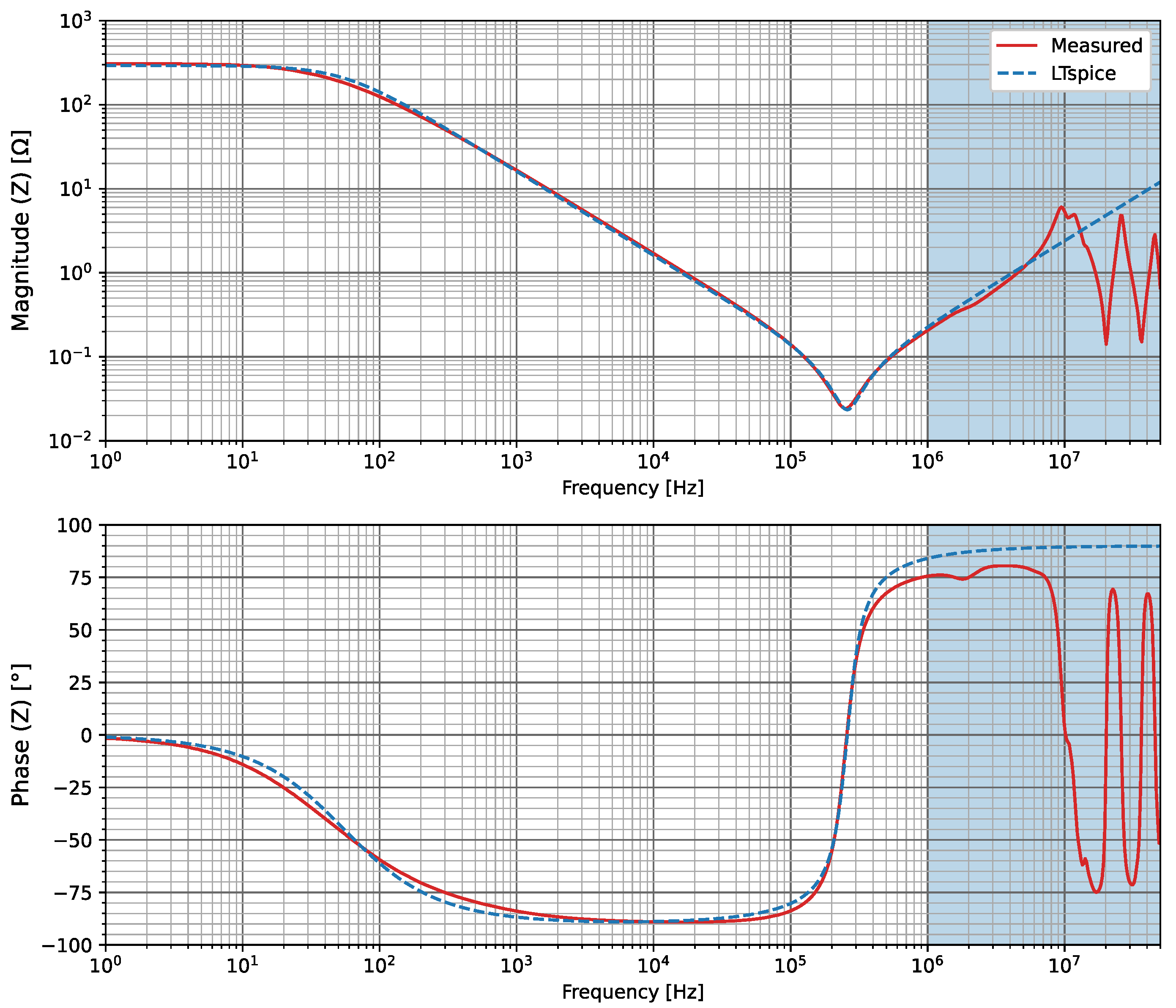
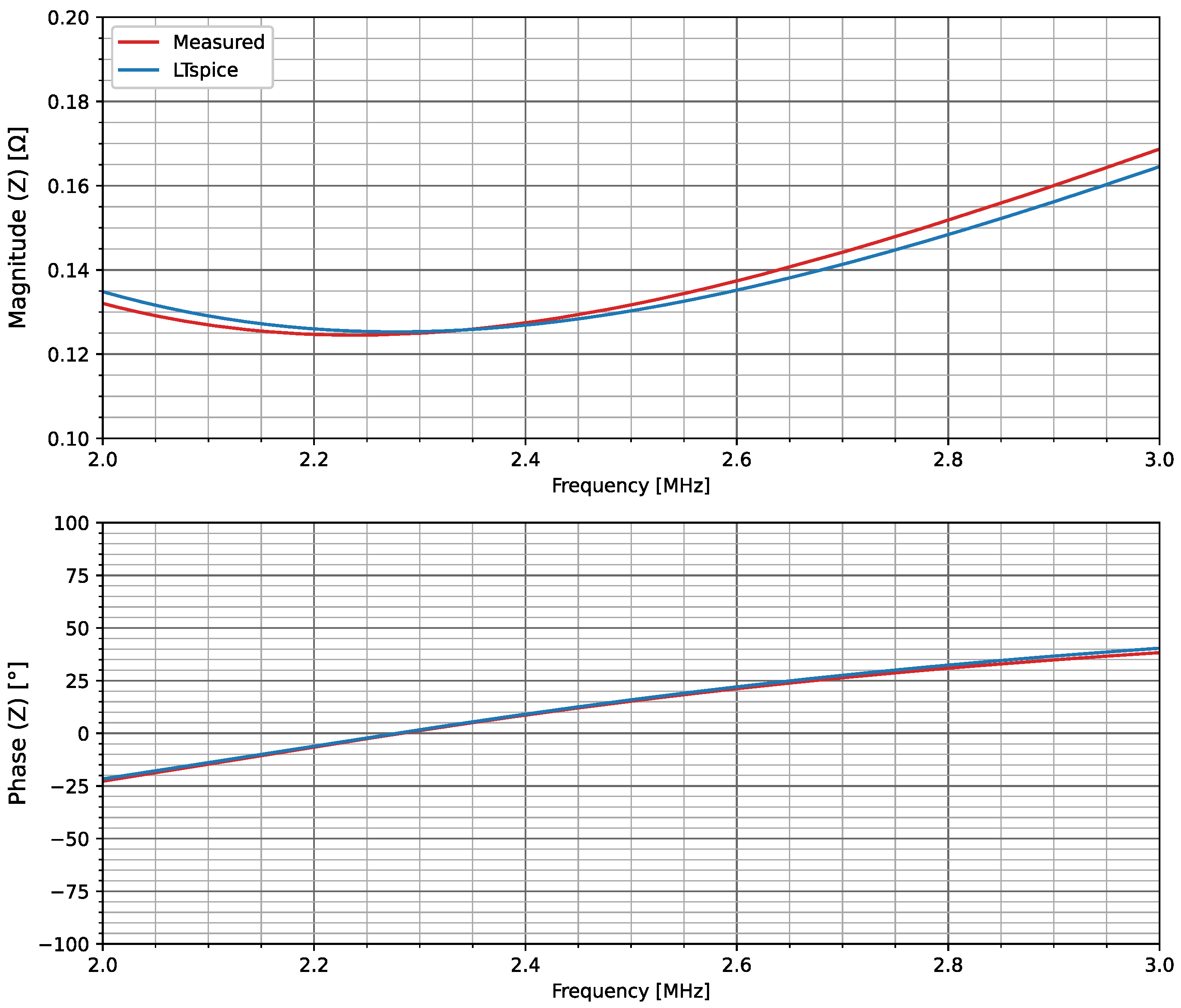
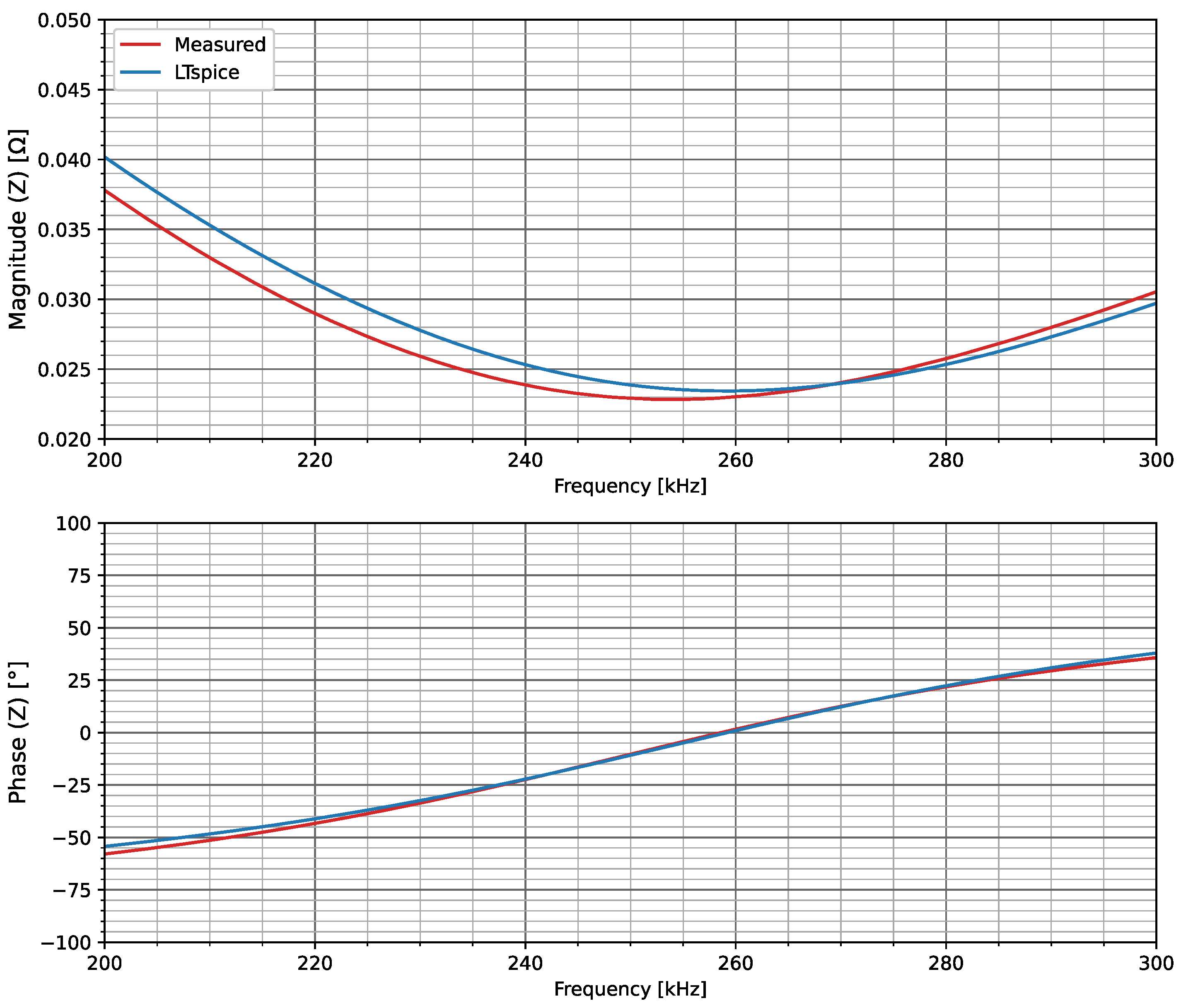
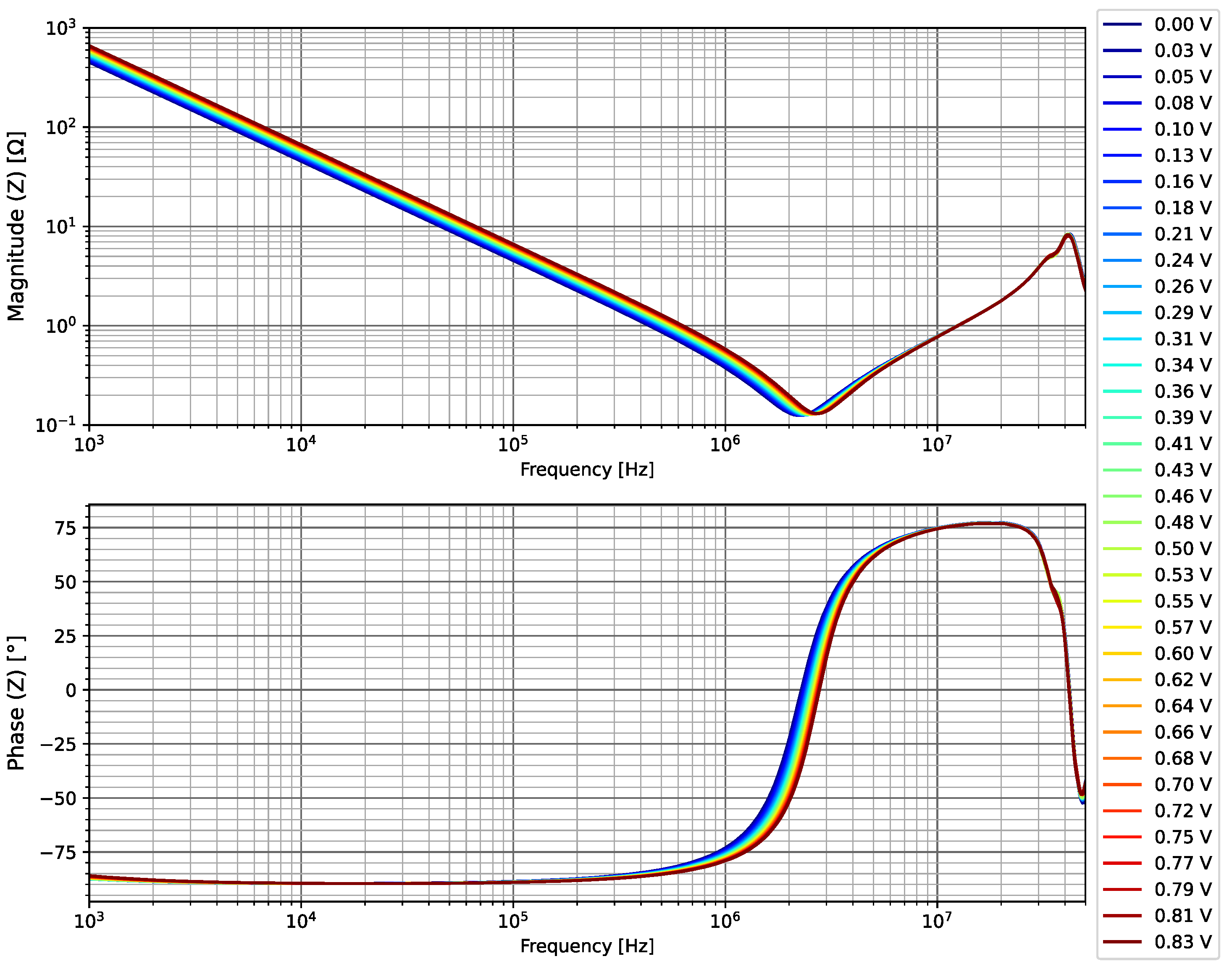
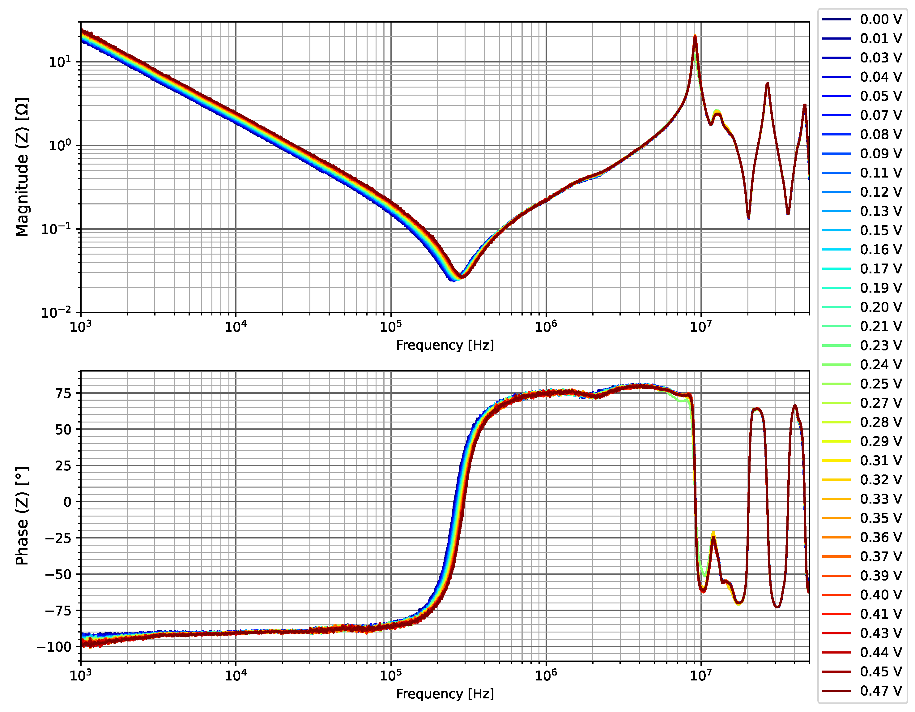
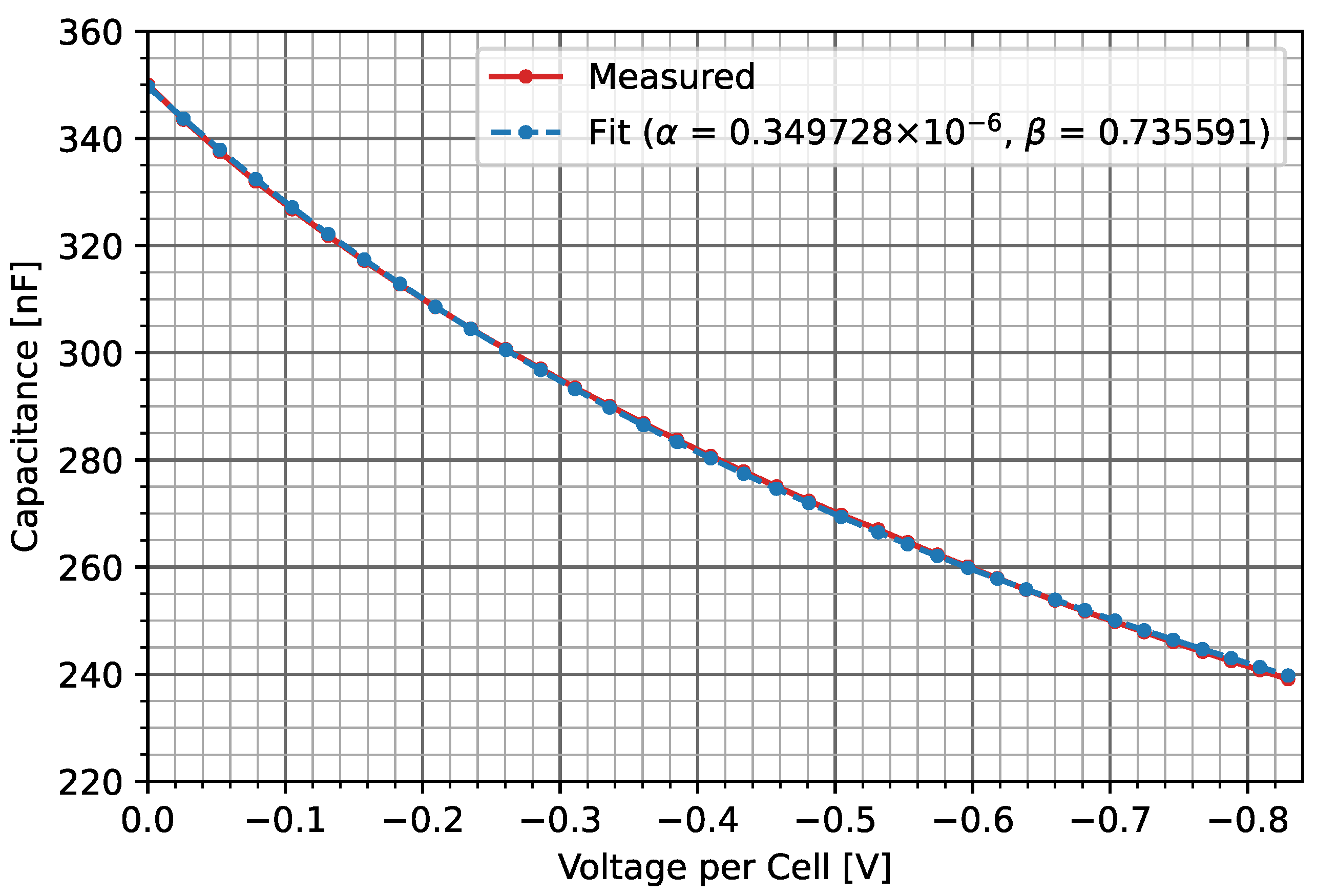
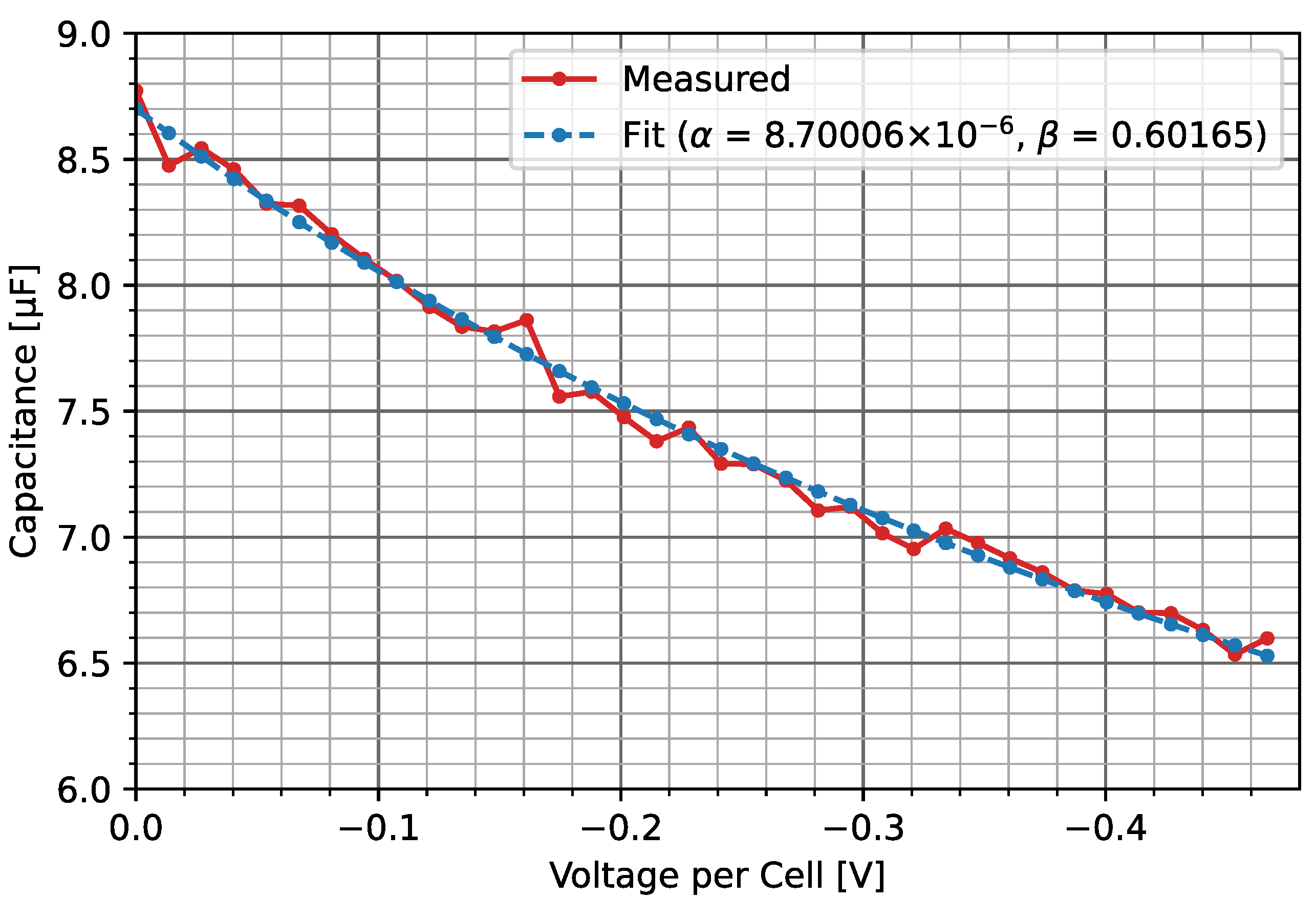
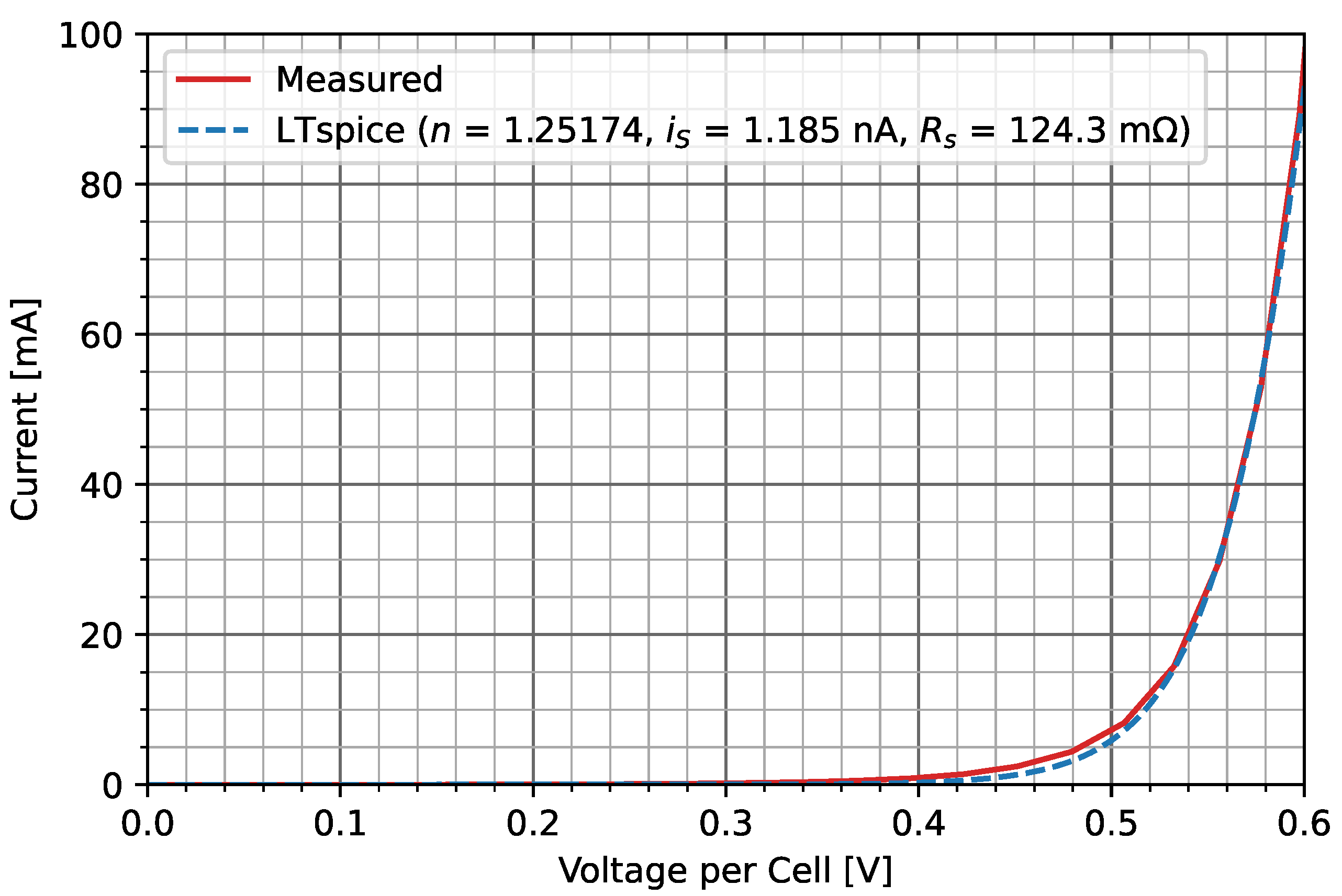
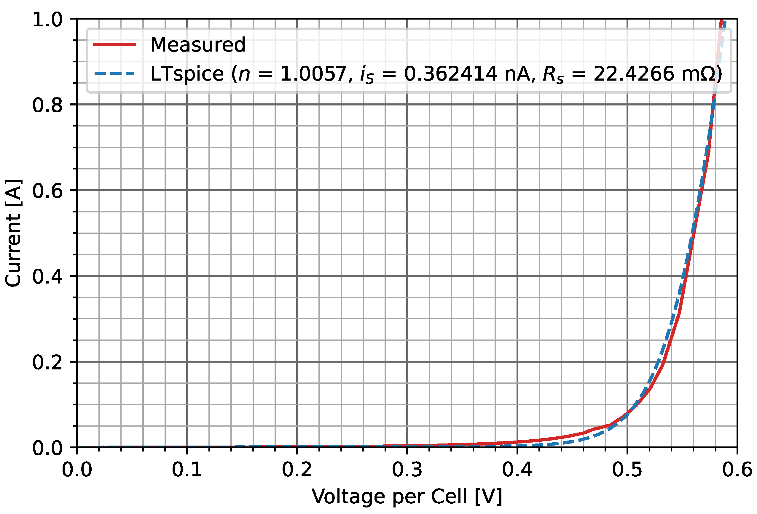
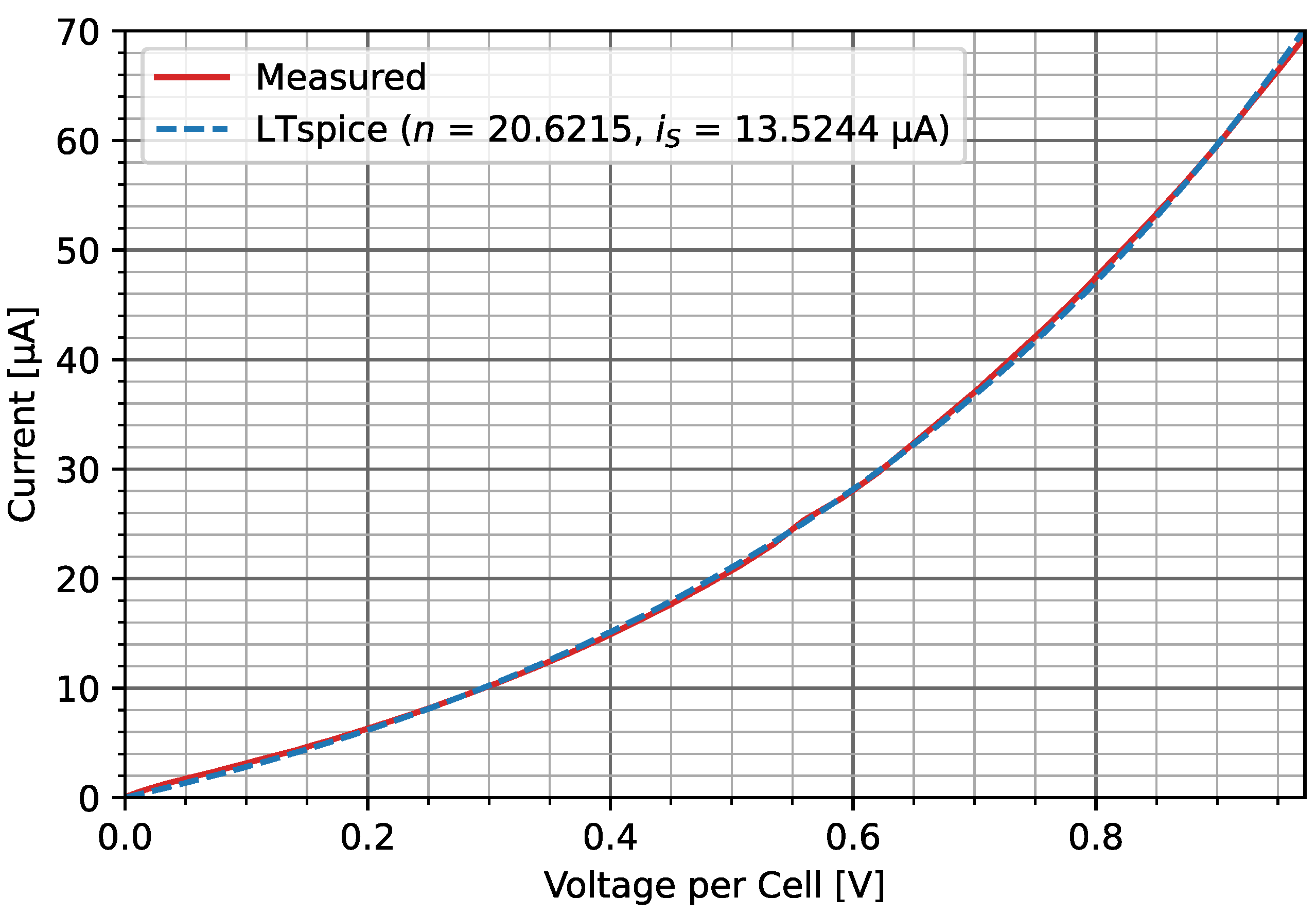
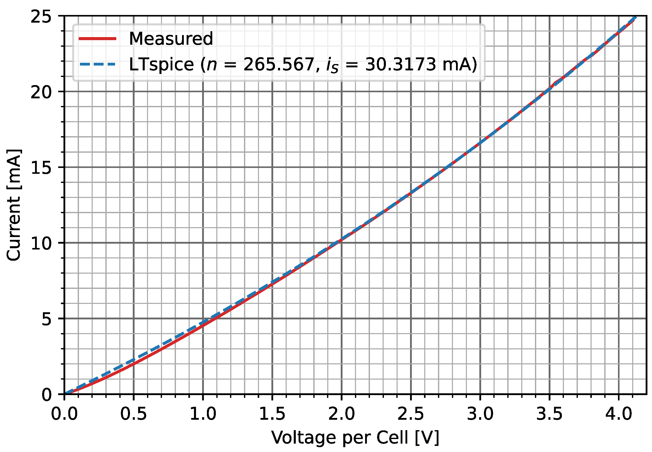
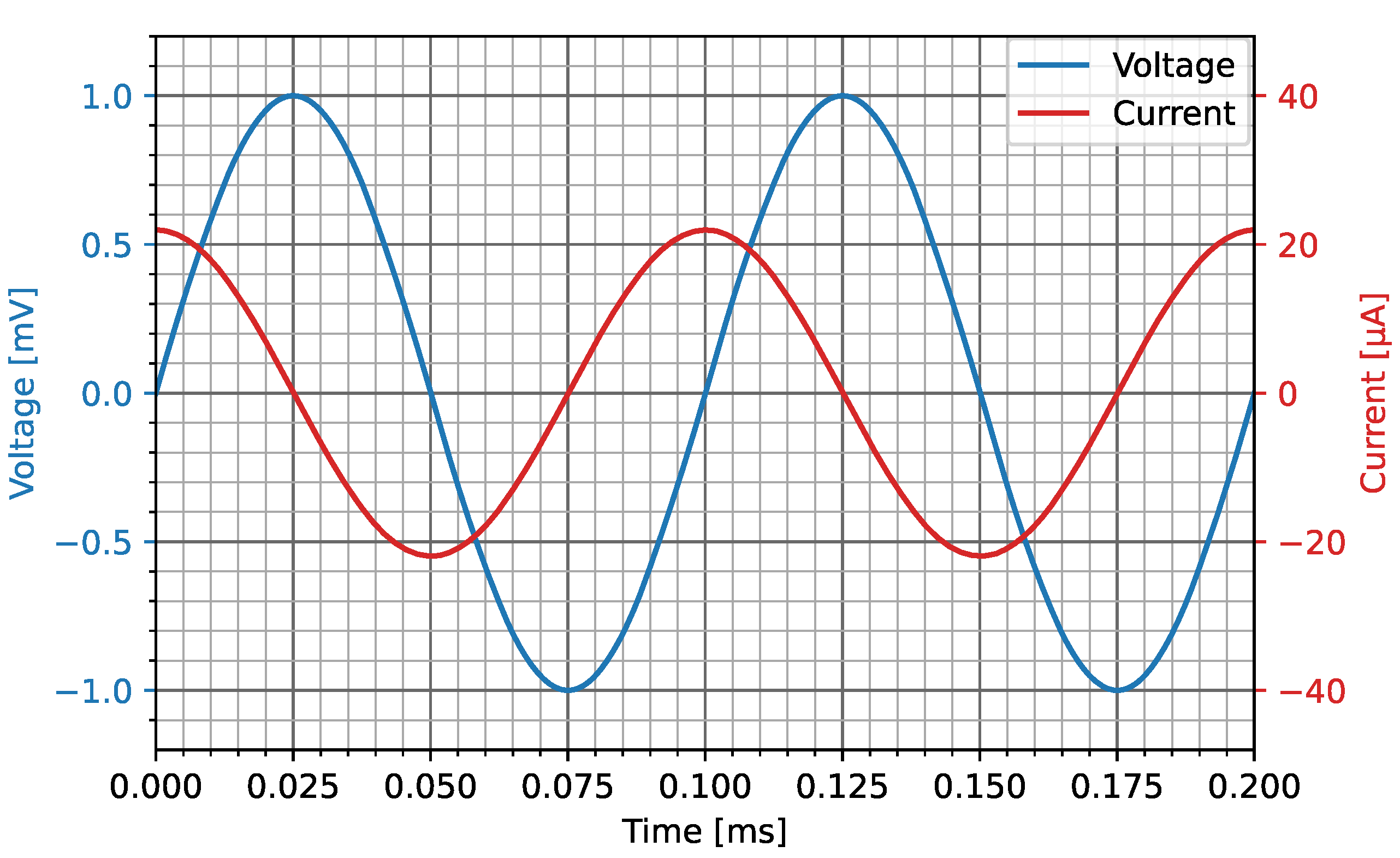
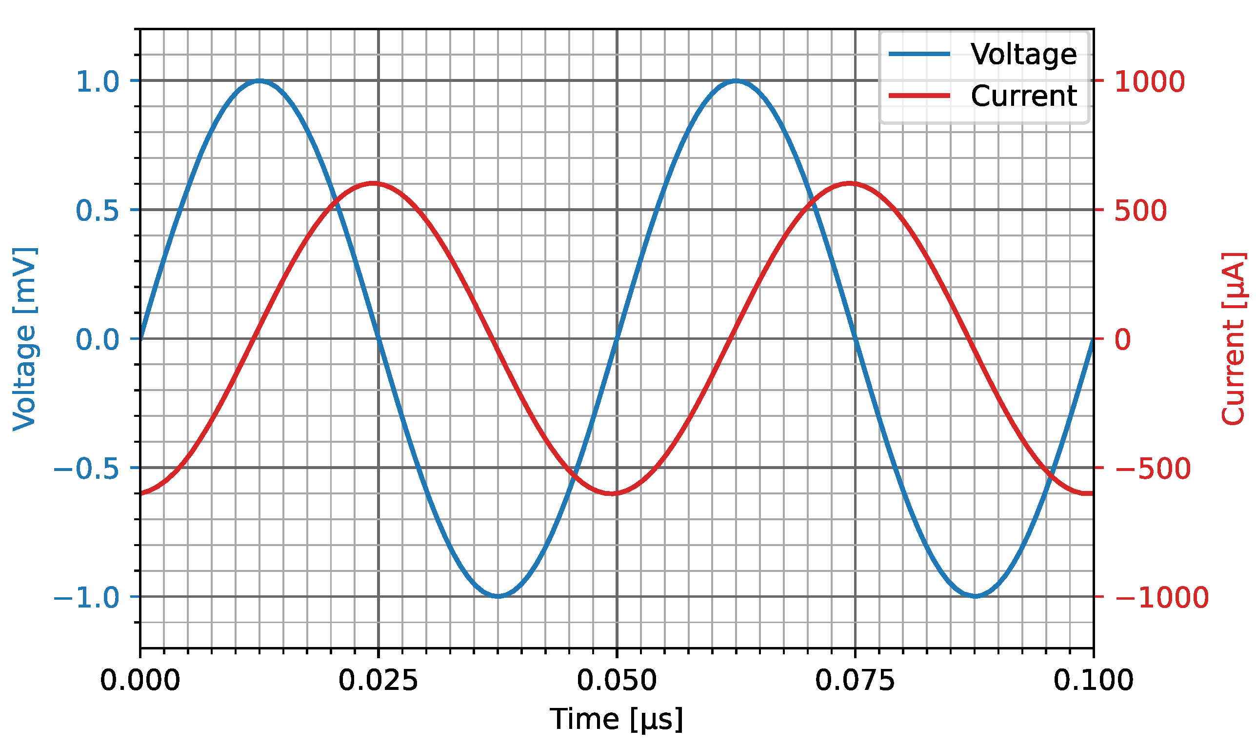
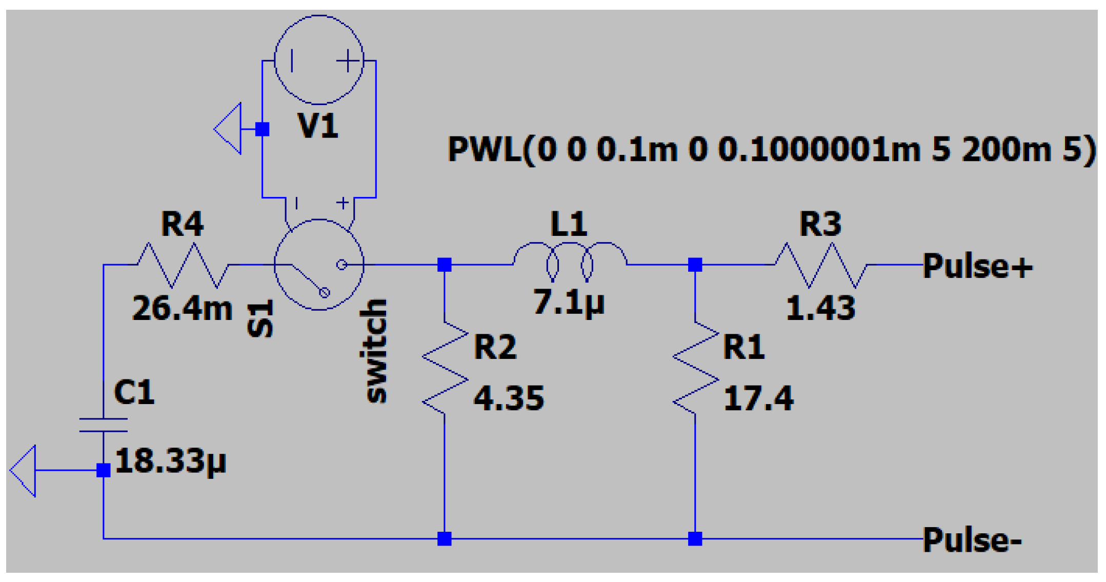
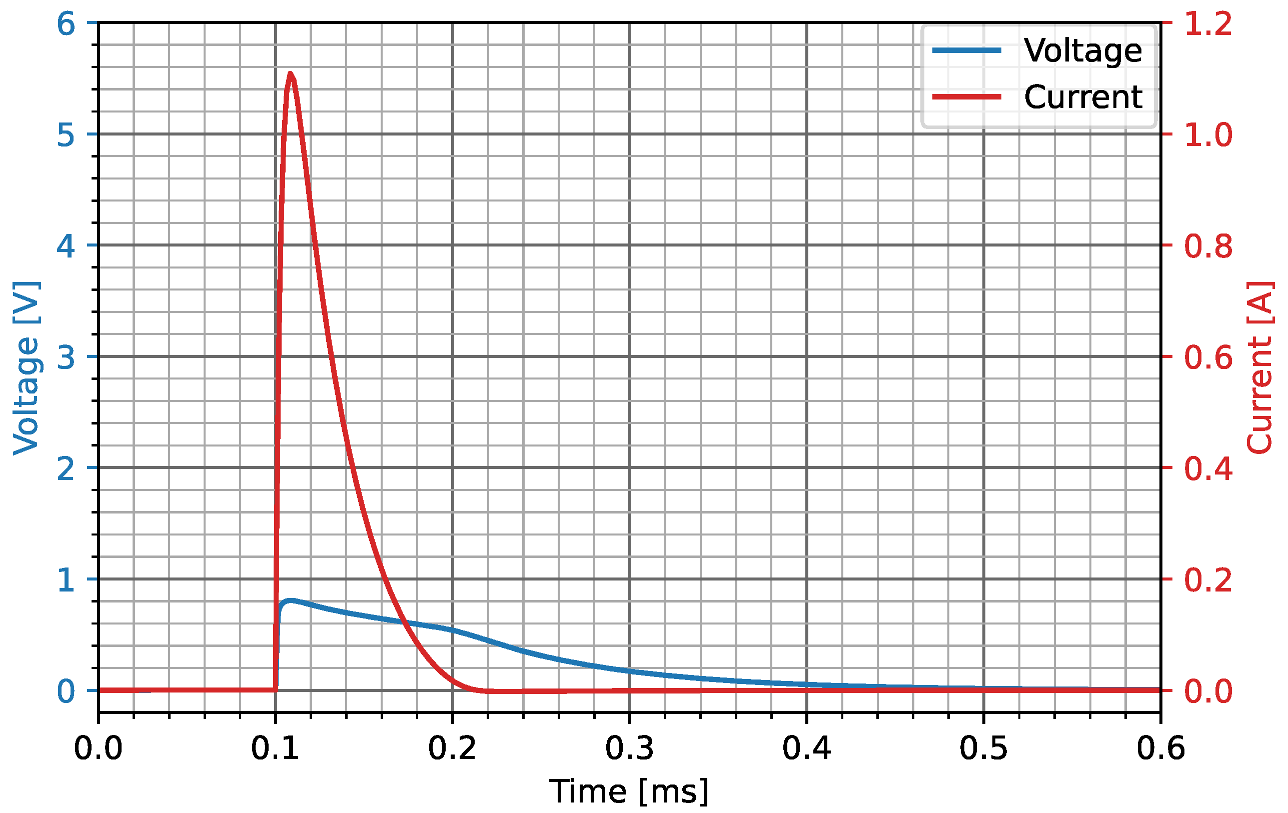
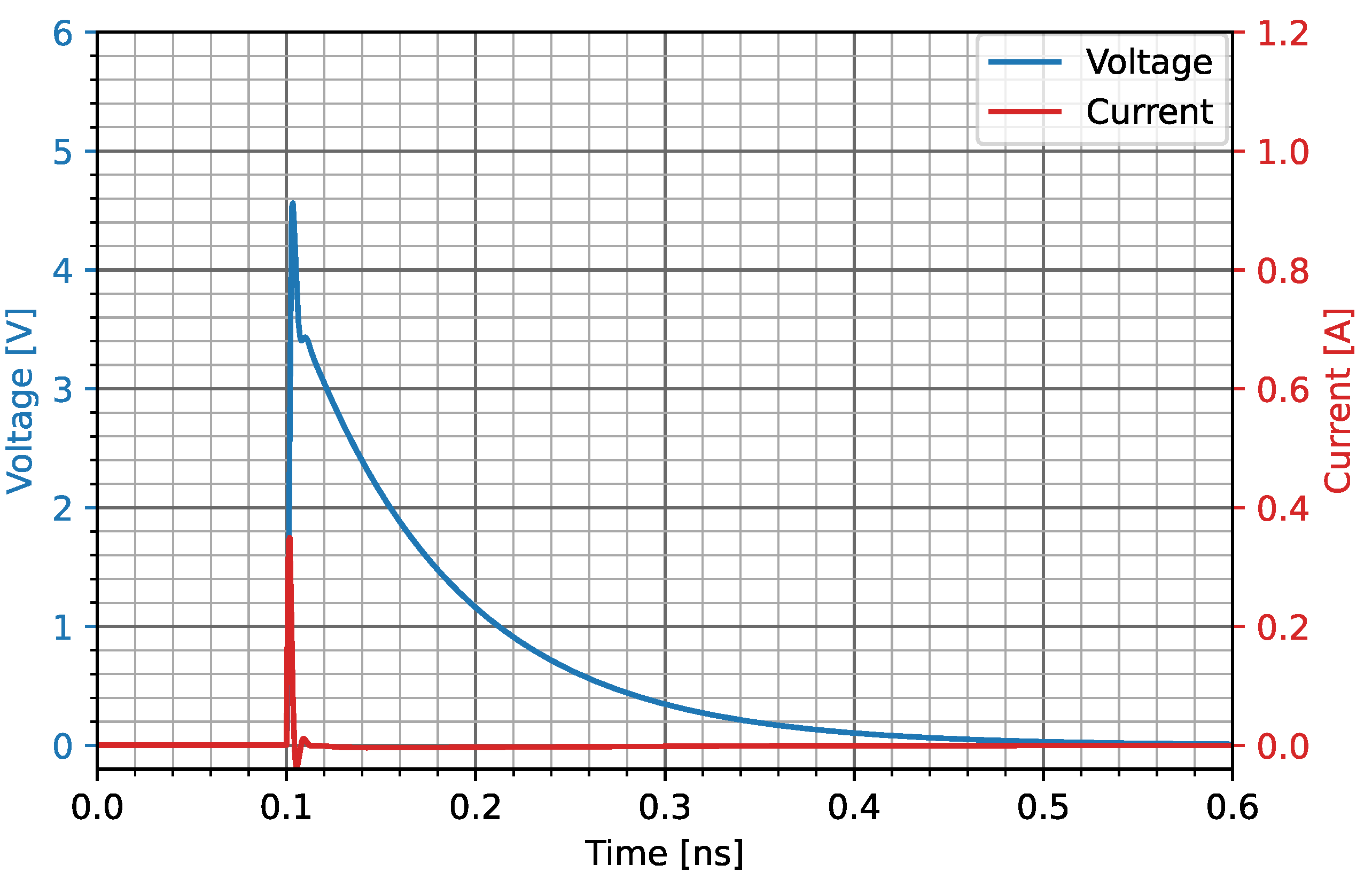
Publisher’s Note: MDPI stays neutral with regard to jurisdictional claims in published maps and institutional affiliations. |
© 2022 by the authors. Licensee MDPI, Basel, Switzerland. This article is an open access article distributed under the terms and conditions of the Creative Commons Attribution (CC BY) license (https://creativecommons.org/licenses/by/4.0/).