1. Introduction
The concept of reliability originated in the aviation field. In the 1950s, reliability engineering emerged and developed in the US military. People began to develop a series of military standards for reliability. In the 1960s, the results of reliability research began to be applied to the civilian industry. Based on this, reliability knowledge gradually formed a somewhat complete theoretical system. Reliability theory can directly affect the quality and cost of products, and indirectly influence the service quality delivered through those products [
1,
2,
3].
Highly reliable power supplies play an increasingly important role in applications such as telecommunication power supplies [
4], electric aircraft [
5,
6,
7], large-scale scientific facilities, high-tier data centers, hospitals, etc. [
8,
9,
10]. In these applications, the continuity of power supply is critical [
11]. However, field experience showed that power devices, such as insulated-gate bipolar transistors (IGBTs) and metal-oxide-semiconductor field-effect transistors (MOSFETs), are vulnerable to failure [
12,
13].
One of the most significant approaches to boosting system reliability is fault-tolerant techniques. To increase the continuity of the power supply, many fault-tolerant methods have been introduced [
14,
15,
16]. The fault-tolerant solutions usually employ hardware redundancy [
17,
18]. Reference [
13] presents a comprehensive review of fault tolerance methods for power electronic converters when power devices fail. The authors summarize four types of fault-tolerant solutions of hardware redundancy and classify them as system level, module level, leg level, and switch level. First, system-level redundancy at least doubles the system cost, while the cost of paralleled power modules operating in
N + 1 mode only increases by 1/(
N + 1). The leg level and switch level generally have two types of faults: open circuit failure (OC) and short circuit failure (SC). Refs. [
16,
19] introduced a topology that configures the full-bridge structure into a half-bridge structure. Nevertheless, it is required that the fault type of the switches is SC fault and other switches on the same bridge must keep open. Ref. [
20] proposed a fault-tolerant direct current (DC)-DC converter derived from a resonant converter. The switch’s failure type is also an SC fault. However, the probability of an OC is fault not less than that of an SC fault, so both faults should be considered, which adds complexity to the hardware solution and operation mode, and is not conducive to the reliability of the power supply. Once the power module fails (whether it is an OC or an SC of components), the module or system generally ends up as an OC because of the protection mechanism. In summary, the module level has more advantages in redundancy and fault tolerance.
At the leg level and switch/component level (we use component level in this article), we can focus on the optimization of design and component selection rather than fault tolerance due to the above analysis. Circuit failures are mostly caused by damaged components. The reliability of components is related to the component’s temperature, voltage (power stress), quality and environmental conditions, etc. It is difficult to improve the reliability of the components by improving the manufacturing technology or environmental conditions for technically mature and quality-qualified components. Temperature is relatively easy to reduce through pertinency design. For electronic components, reliability is a function of temperature, and they are positively correlated. The reliability and lifetime of a transistor directly depend on its operation temperature [
21,
22]. Wang proposed in [
23] that the transistors have the highest failure rate in power electronic converters due to temperature fluctuations. They found that during the operation of the IGBT, the heat generated by the semiconductor power loss will be transmitted to the heat sink to produce junction temperature fluctuations, causing the bond wire to generate shear stress at its welding point, and the changing stress produces cracks that cause the bond wires to fall off. In the design process of the power module, special attention should be paid to devices with high power and high heat. Devices with low reliability are often high-power devices, such as transistors, inductors, capacitors, and sampling resistors. Because the transistor is the core device of current conversion and the structure is complex, it not only has high power but also low reliability. To reduce the heat of the transistors, the buck circuit of the SLAC National Accelerator Laboratory power system is designed with two bridge arms that work alternately to reduce the switching frequency by half, and MOSFETs are used to replace the freewheeling diode to obtain a smaller resistance [
24,
25]. Therefore, at the leg level and component level, we can reduce the operating temperature of the power supply through methods such as topology design, derating design, and operation strategy [
26].
At the module level, the redundant structure of
N + 1 modules can significantly improve the reliability of the power supply [
27], while it is also important to improve the reliability of each parallel module. The design and operation strategy at the leg level and component level are important factors [
28].
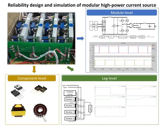
In this article, we have conducted a comprehensive analysis of the reliability design of high-power current sources. We propose a set of methods for power reliability design at the module level, leg level, and component level. The new approaches in this paper are as follows:
- (1)
At the module level, we proposed the most favorable form and the operation strategy of module redundancy for power supply reliability, and provided an analysis method to determine the optimal number of parallel modules;
- (2)
At the leg level, we reduced the power consumption and temperature of the transistors by utilizing the zero voltage switching (ZVS) characteristics of the PSFB topology;
- (3)
At the component level, we reduce the power consumption and temperature of the components through derating design. We calculated the design parameters of the components and set aside margins when selecting the components.
In
Section 2.1, we analyze and compare three forms of power redundancy, and choose the optimal form and the optimal number of modules. Then we show the of design the overall structure of the power supply and the topology of each module. In
Section 2.2 and
Section 2.3, we propose reliability design methods at the leg level and component level of the power supply respectively. In
Section 2.4, we point out the effectiveness of the power supply reliability design and some reliability weaknesses through the analysis of the power consumption of key components of the power supply. In
Section 3, we simulate the power redundancy strategy and the design of key parts, and we also verify the correctness of the design parameters. The conclusions of this paper are summarized in
Section 4.
2. Design of the Highly Reliable Current Source
2.1. Selection of Redundancy Forms and Design of Fault Tolerance Mechanisms at the Module Level
2.1.1. Selection of Redundancy Forms
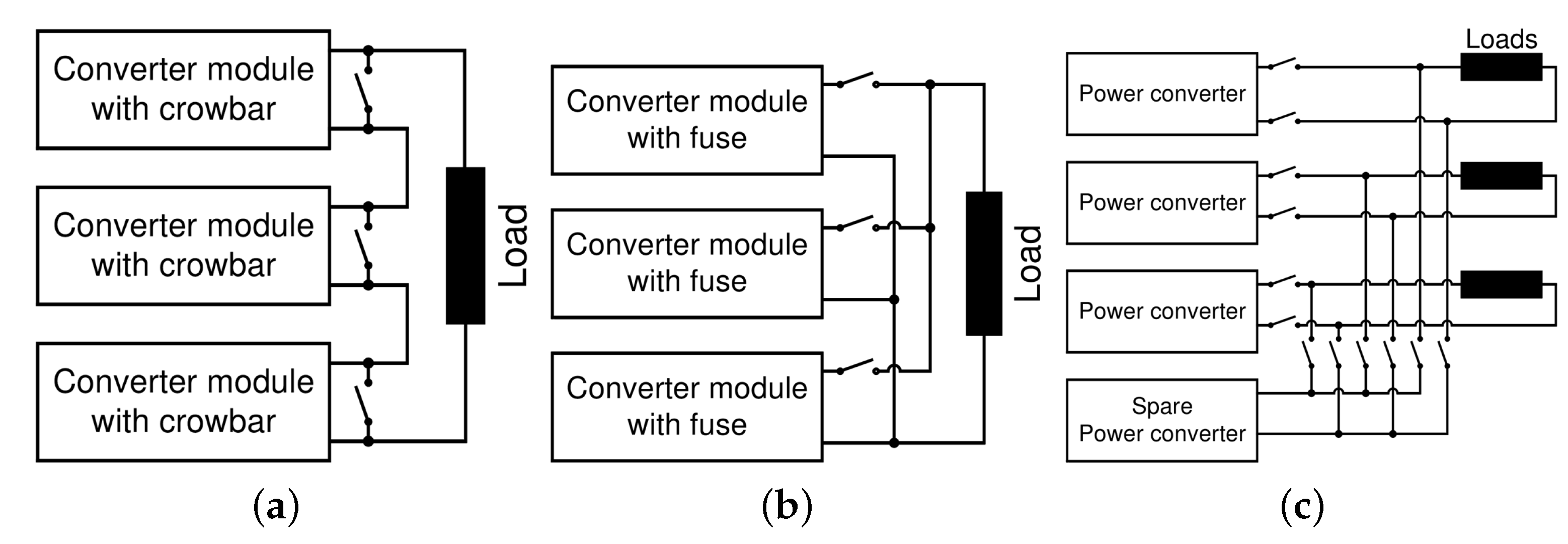
Module redundancy can significantly improve the reliability of the power supply. The first thing we need to determine is the form of redundancy. Redundancy can be designed in three forms: series redundancy, parallel redundancy, and hot spare [
29], as shown in
Figure 1. We will analyze the reliability advantages of the form of redundancy we chose and the fault-tolerant approach we designed.
We know that the power module in
Figure 1a is a voltage source and the power module in
Figure 1b is a current source because voltage sources are not allowed in parallel and current sources are not allowed in series. Additionally, the failure of the module is almost always OC as described earlier. When a module in
Figure 1a fails, the crowbar must be used to short-circuit the module, while in
Figure 1b, when a module fails, there is no need to deal with the module (in the case of an SC, the fuse is burned, and the module is still OC). The crowbar structure in
Figure 1a will introduce additional risks to the reliable operation of the power supply. Moreover, each module in
Figure 1a outputs 1/3 the voltage, and each module in
Figure 1b outputs 1/3 the current. The transistors usually have a far greater ability to bear voltage than to bear current, so it is more reasonable for all modules to share the current in the design of high-power power supplies. For
Figure 1c, which is called hot spare, when a module fails, the switching control of the backup module is difficult. Additionally, the backup module needs to be connected to every power supply module, so the circuit is complicated. When designing for power availability, we should simplify the circuit rather than increase the complexity. Moreover, when the backup module is switched, the output voltage or output current of the power supply fluctuates greatly, which also affects the reliability of the power supply. Therefore,
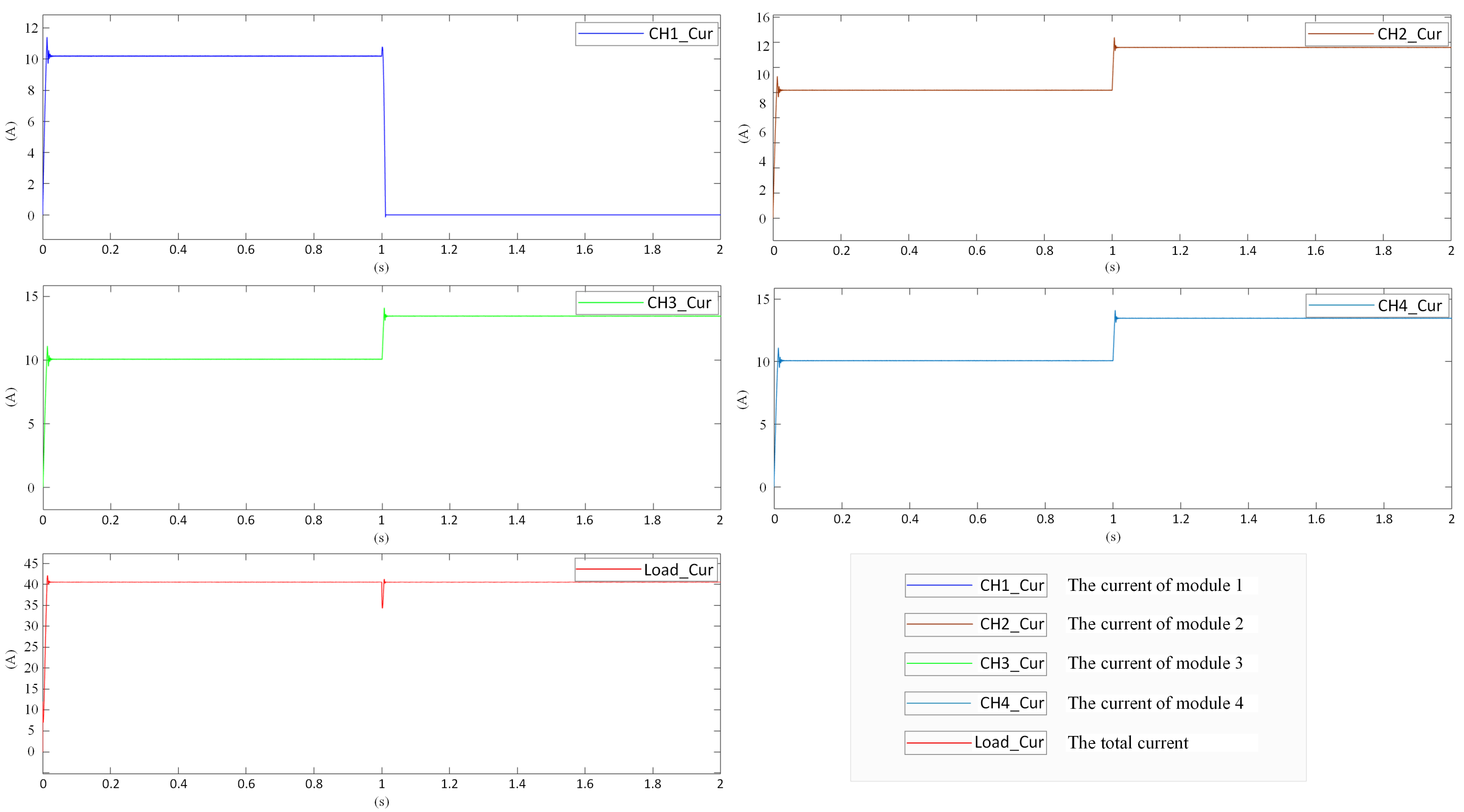
Figure 1b’s redundant structure has more advantages in reliability. The operation mode is that each module runs below the rated current. When one module fails (OC), the remaining modules increase the current, work at the rated power, and the total output returns to the state before the failure. Each module operates with derating, resulting in lower power consumption, lower temperature, and higher reliability.
2.1.2. Determination of the Number of Modules
The choice of how many modules to connect in parallel is based first on the needs of the actual situation. We analyze the optimal number of modules from three factors, reliability of power modules, current fluctuations after failure, and cost. Mean time between failures (MTBF) was chosen as the evaluation parameter for reliability. The formula for calculating the reliability of the
N + 1 system is as follows [
30].
where
N is the number of modules and
is the failure rate of each power module working at rated power. The equation shows that the
of the
N + 1 system is a decreasing value over time, unlike most products which are constant. Additionally, since the power supply system is repairable, we assume that the reliability of the power supply is approximately restored to its highest level after each repair, so the
of the
N + 1 system decreases periodically. We assume that the power supply system is repaired in the 12th month of each year, then the
of the power supply system reaches the minimum value at the end of the 11th month, and we take this value, so
t = 8016 h. We have surveyed the products of our partner power supply manufacturers and found that the
of power supply modules is mostly between 1 year and 10 years. To simplify the calculation, we set
h and
h to approximately represent the number of hours of 1 year and 10 years, respectively. The corresponding module failure rates
are
h and
h, respectively. We get the
Table 1.
From
Table 1, we know that when
h, the lowest
of the 4 + 1 power supply is higher than the
of a single module; when
h, the lowest
of the 6 + 1 power supply is higher than the
of a single module. and the higher the
of a single module, the more obvious the reliability advantage of the
N + 1 power supply. For the current fluctuation after the fault, if the power supply is in the form of a hot spare, the delay time for the standby module to replace the faulty module is long, so the current usually fluctuates around 1/
N + 1 [
31]. If the redundant form of
Figure 1b is used, due to the freewheeling capability of the inductor in the power supply, the current fluctuation range after a module fault will not exceed I/(
N + 1) (where I is the rated current), which is also an advantage of this structure. The current fluctuation is usually in the range of (0.2 0.6)I/(
N + 1) [
15,
32,
33]. In this paper, we choose 0.4I/(
N + 1). Regarding the cost, in order to simplify the calculation, we set the cost of the power supply without redundancy as C, and the cost of
N + 1 power supply increases by at least C/
N. To display the curves of the three variables in the same coordinate, we normalized the variables, as shown in
Figure 2.
We hope that the current fluctuation and the proportion of additional costs are small and the MTBF is large. In
Figure 2, when the number of power modules is 2 + 1, 3 + 1, and 4 + 1, the curvature of the three curves is large. That is to say, the power supply obtains the best cost performance in this interval. Therefore, the 3 + 1 or 4 + 1 form is more reasonable. In this paper, we choose four power modules, that is, the 3 + 1 form.
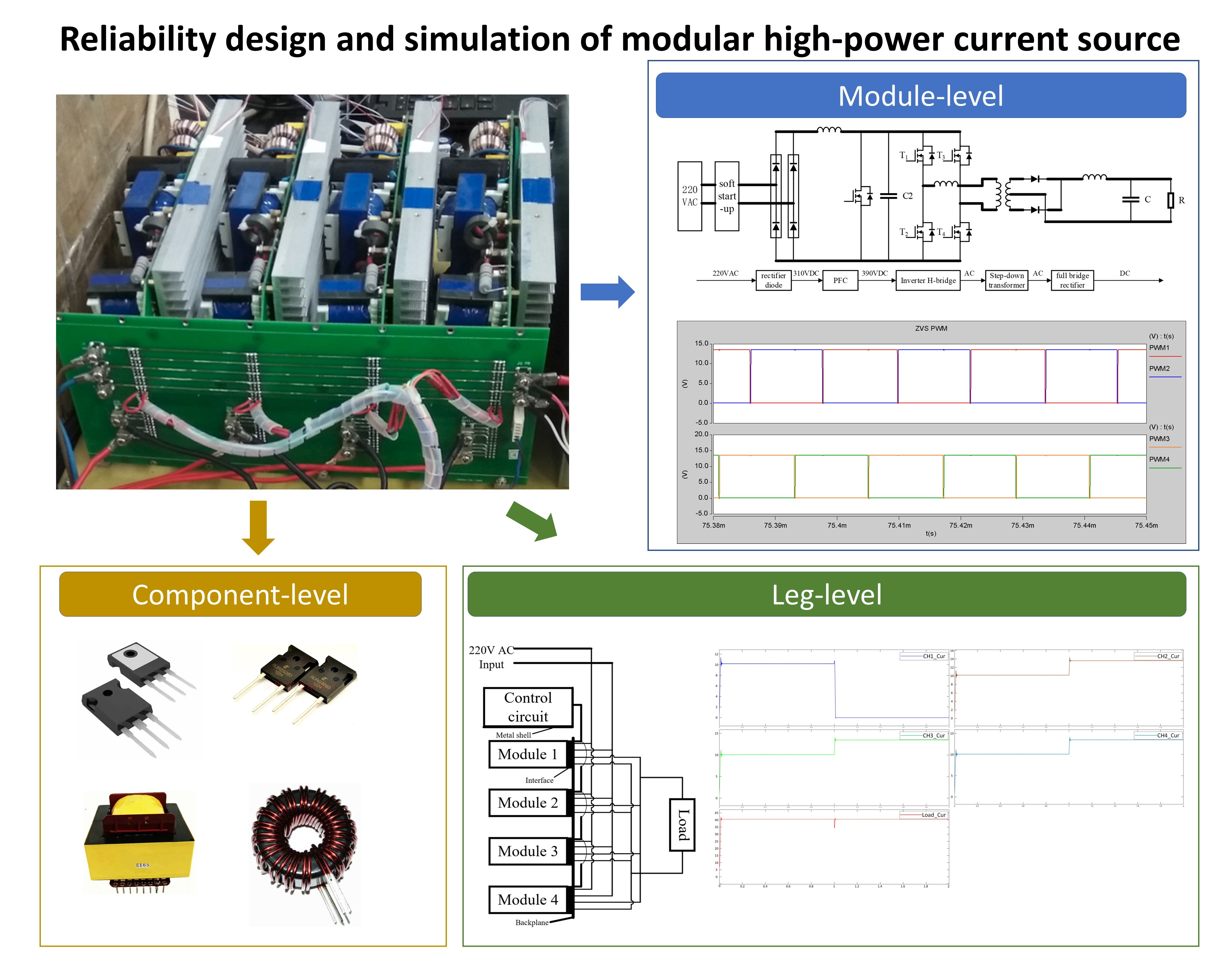
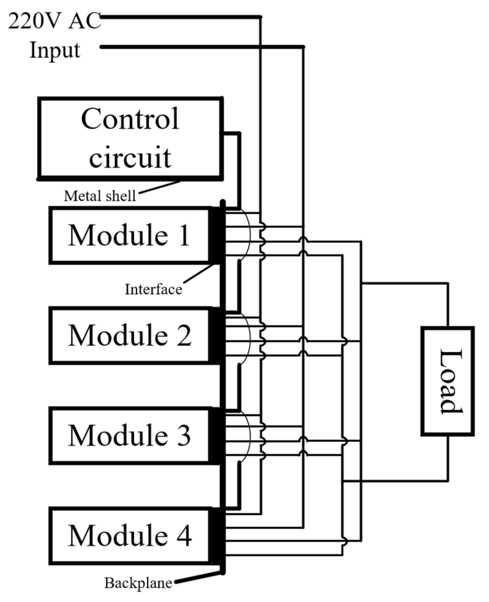
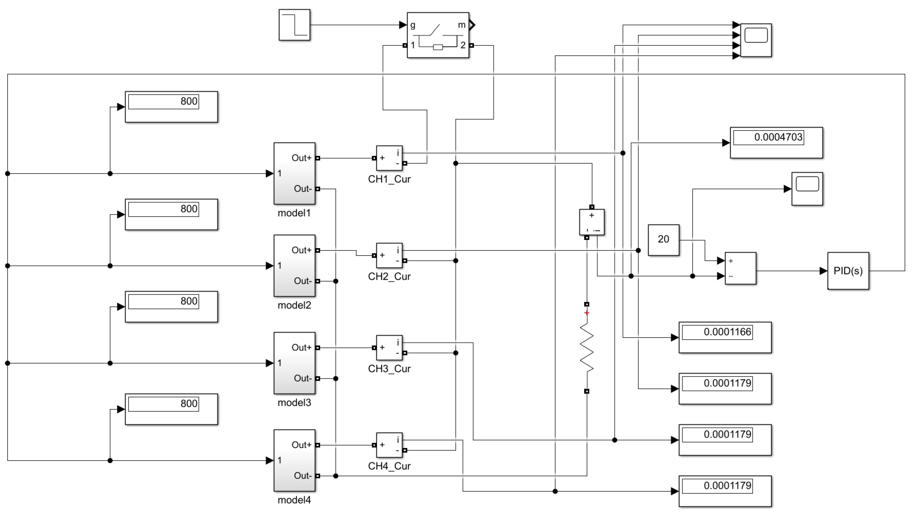
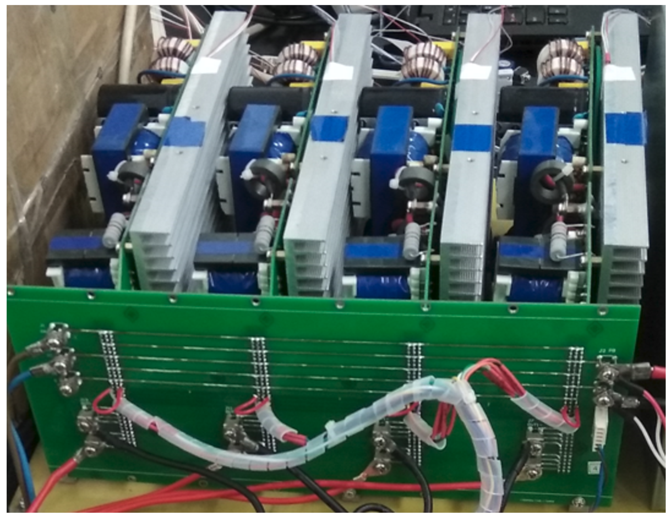
We use a backplane to connect four identical power modules in parallel. The power control circuit is arranged in the control box, and the control box uses a metal layer to shield the signal interference of the power module. The block diagram of the power supply design is shown in
Figure 3.
2.1.3. Main Parameters and Topology of the Module
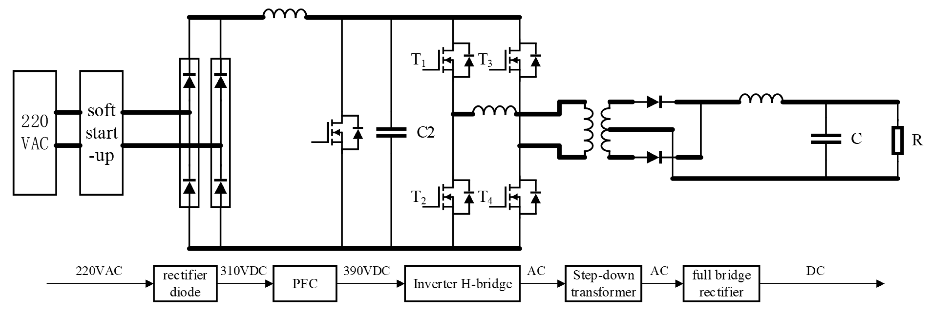
After we determine the form of redundancy, we need to design the topology of each module of the current source. We added a power factor correction (PFC) structure to the front part of the power supply, not only to improve the power factor of the power supply but also to reduce the pollution of the power supply to the grid. The object of our research is high-power current sources, so we tried our best to make the power of the prototype as high as possible, each module was designed to 1000 W. At the output side, we use a transformer to achieve step-down and isolation to get a low-voltage, high-current output, which is very important for the safety of the experimenters. On the main side of the transformer, we need to design an H-bridge to change DC to alternating current (AC) so that the power can be transferred through the transformer. This also prepares the ground for the realization of ZVS. The main system parameters of the module are shown in
Table 2.
The topology of the power module is shown in
Figure 4.
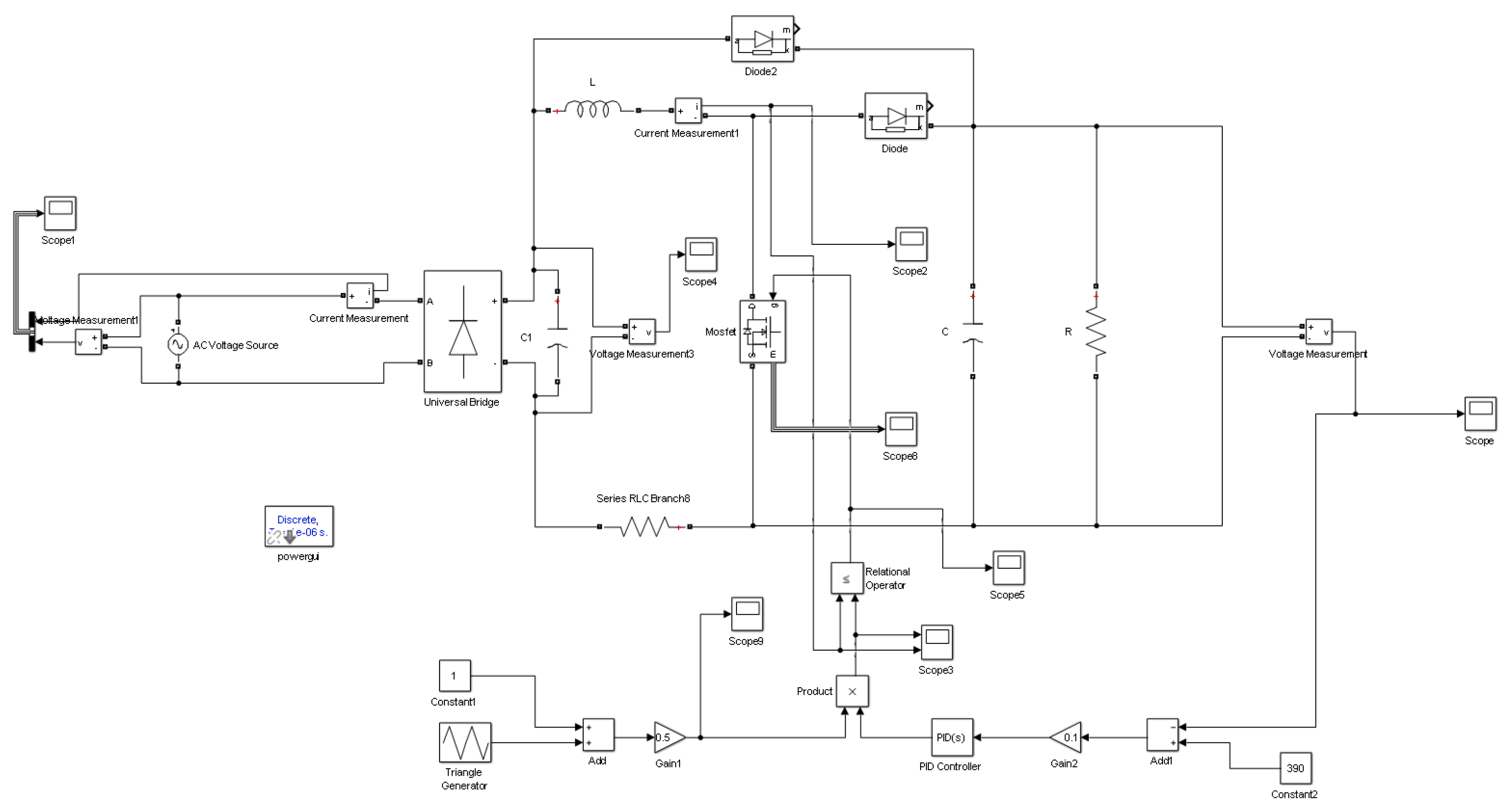
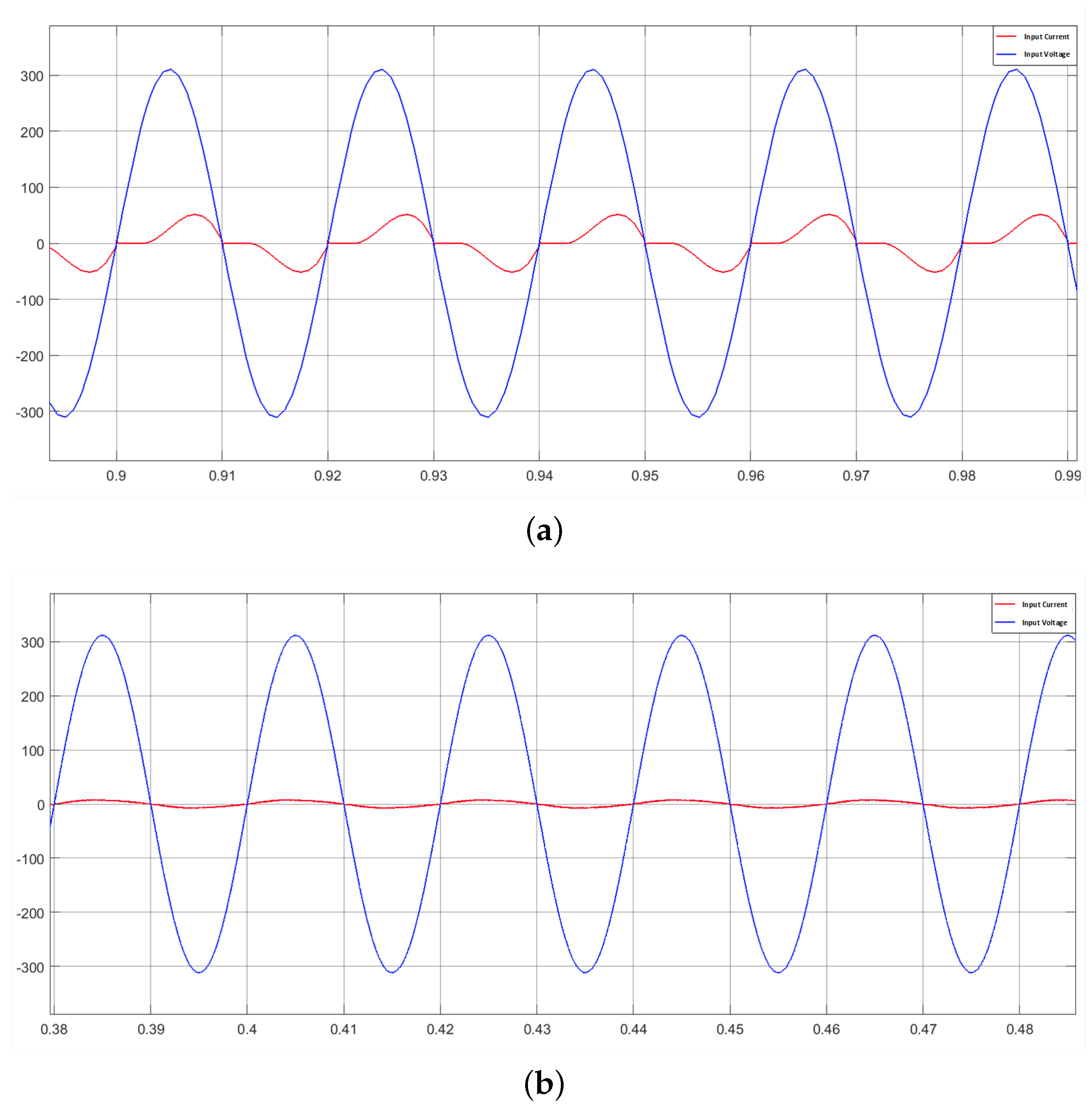
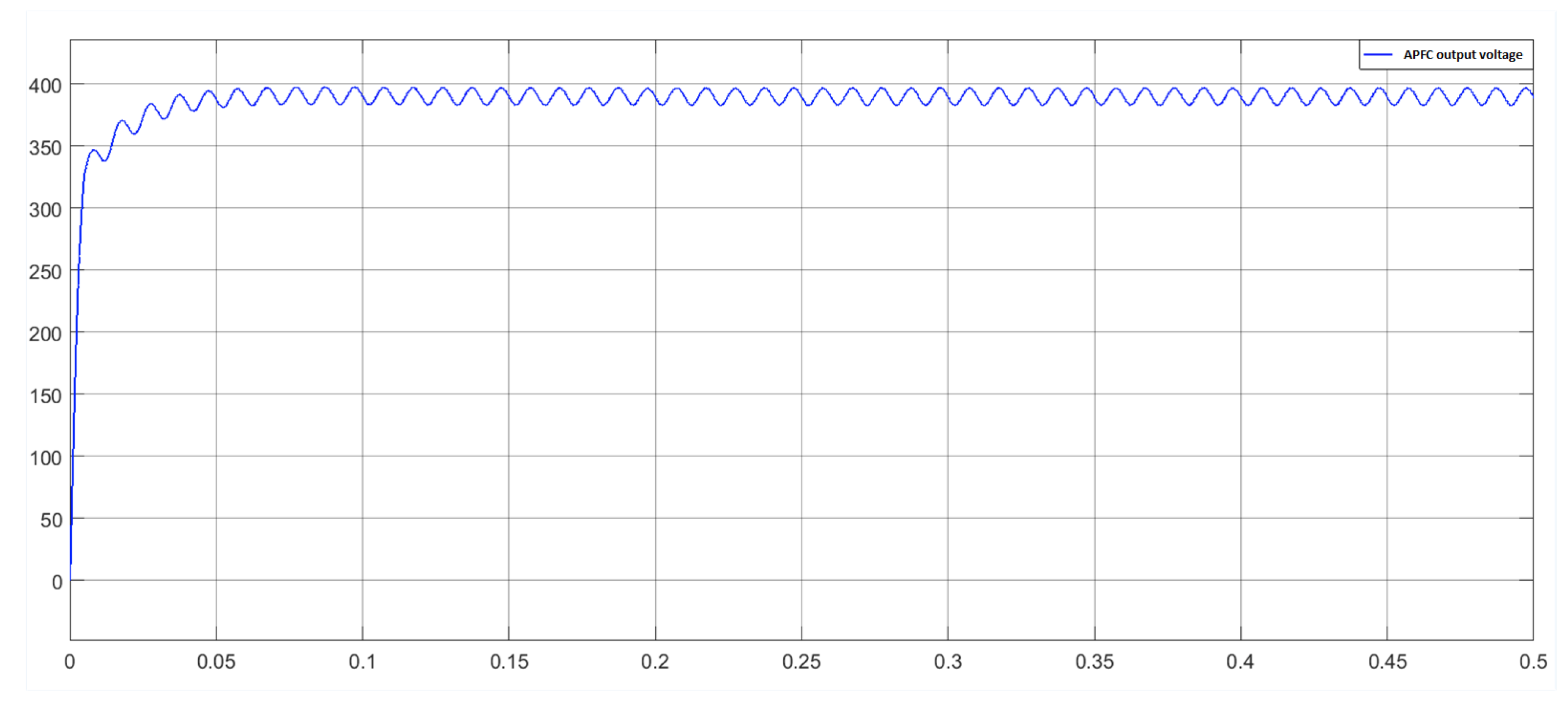
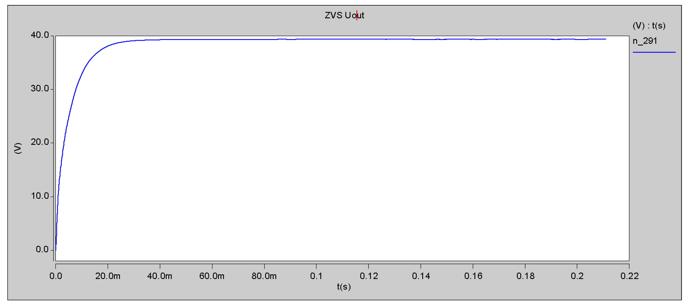
The power supply mainly includes two parts: power factor correction (PFC) and DC/DC. A PFC circuit is added before the converter. The power factor and power of the power supply can be improved. First, 220 V AC is rectified and filtered into about 310 V DC voltage, and then boosted to about 390 V by PFC BOOST. The DC/DC section contains inversion and rectification. The 390 V voltage is inverted by the H-bridge. After inversion, the transformer is used to step down and boost the current. The transformer also plays the role of isolating the high voltage to ensure the safety of the operator. Finally, full-wave rectification is performed to output 50 V/20 A DC power. The module power is designed to be 1000 W.
2.2. Design of PSFB Topology at the Leg Level
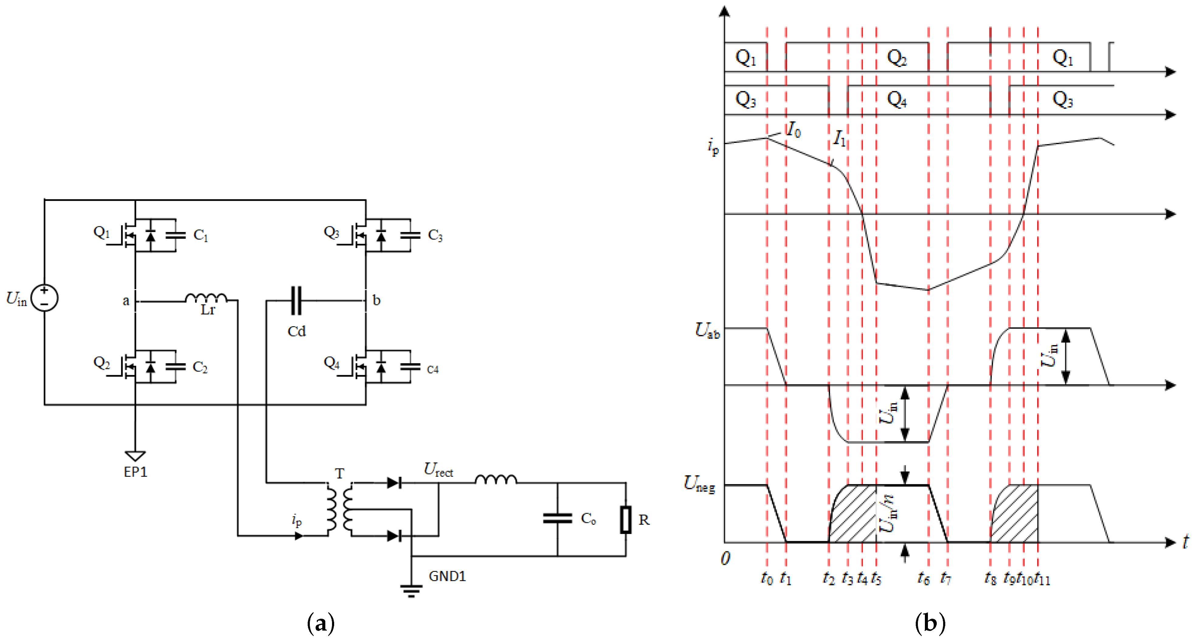
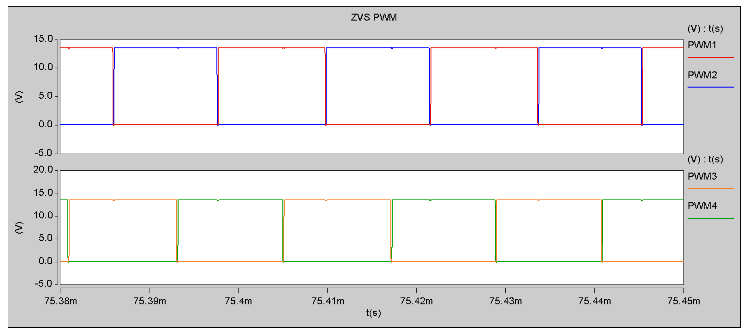
The reliability model of each power module is a series model (that is, if any one device is damaged, the power supply will fail). As mentioned above, when objective conditions such as environment and manufacturing process are determined, temperature is the factor that most affects the reliability of electronic devices. The reliability of electronic devices is a function of temperature, and the two are inversely related. Usually, high-frequency devices consume more power, such as transistors, sampling resistors, diodes, high-frequency inductors, and capacitors. The heat generated by power consumption will cause the temperature of the device to rise, and the failure rate of electronic components such as switches and inductors will be greatly increased at high temperatures. Among all the components, the transistors have the highest manufacturing complexity and the lowest reliability. Therefore, besides cooling, it is necessary to reduce the loss of the transistors as much as possible. In this paper, we use PSFB to realize ZVS [
34], which can greatly reduce the temperature of transistors operation. The circuit is shown in
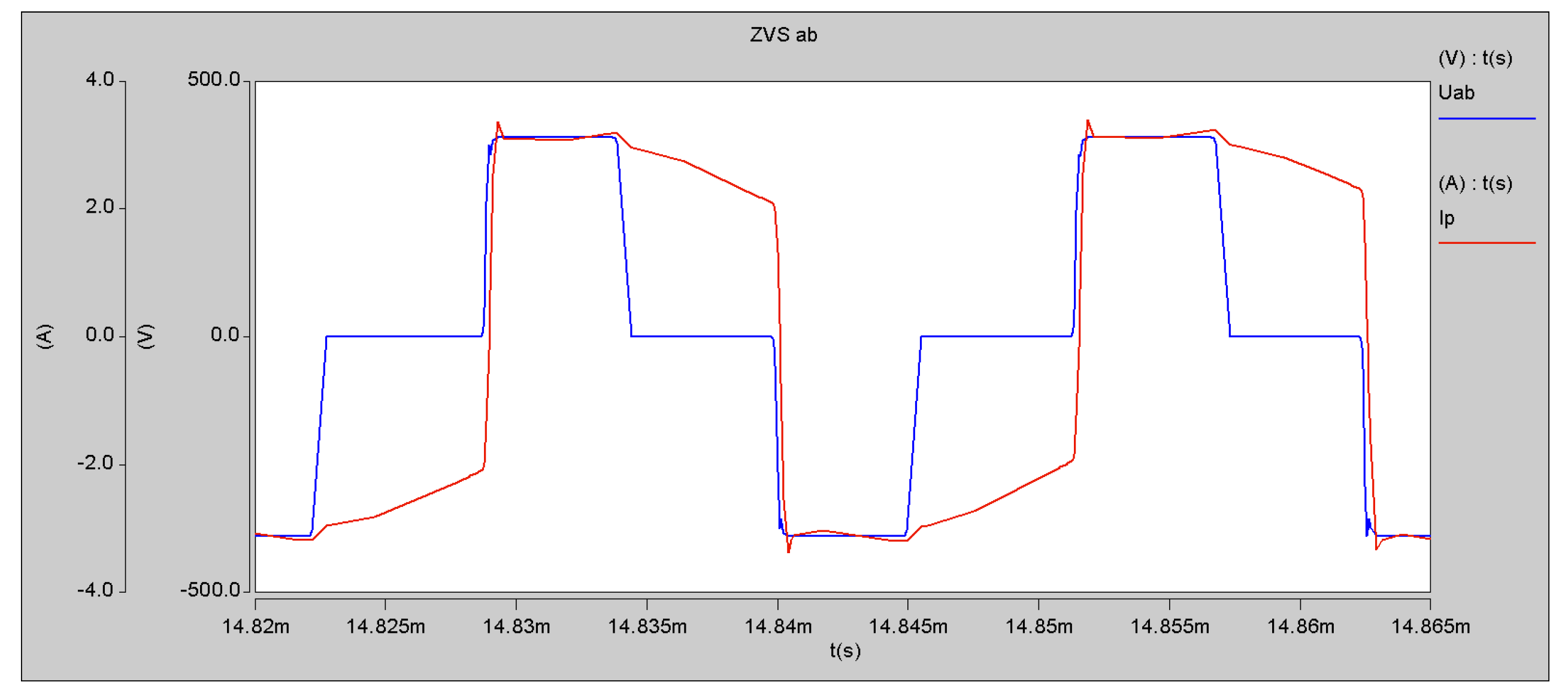
Figure 5a. Q1–Q4 are transistors, C1–C4 are capacitors, Lr is the resonant inductor (including the leakage inductance of the high-frequency transformer), the capacitor Cd is the blocking capacitor, and T is the high-frequency transformer. Using the junction capacitance of the power components and the leakage inductance of the transformer as the resonant element, the resonance is realized in the dead time, so that the four transistors of the H-bridge are turned on and closed at zero voltage in turn to achieve ZVS. The ZVS of the leading leg is affected by output filter inductance and transformer leakage, while the lagging leg is affected by leakage inductance. There are 12 operating modes of PSFB during a complete operating cycle, as shown in
Figure 5b. The positive and negative half-cycles are symmetrical to each other, and each has six operating modes, including two freewheeling processes and four resonance processes.
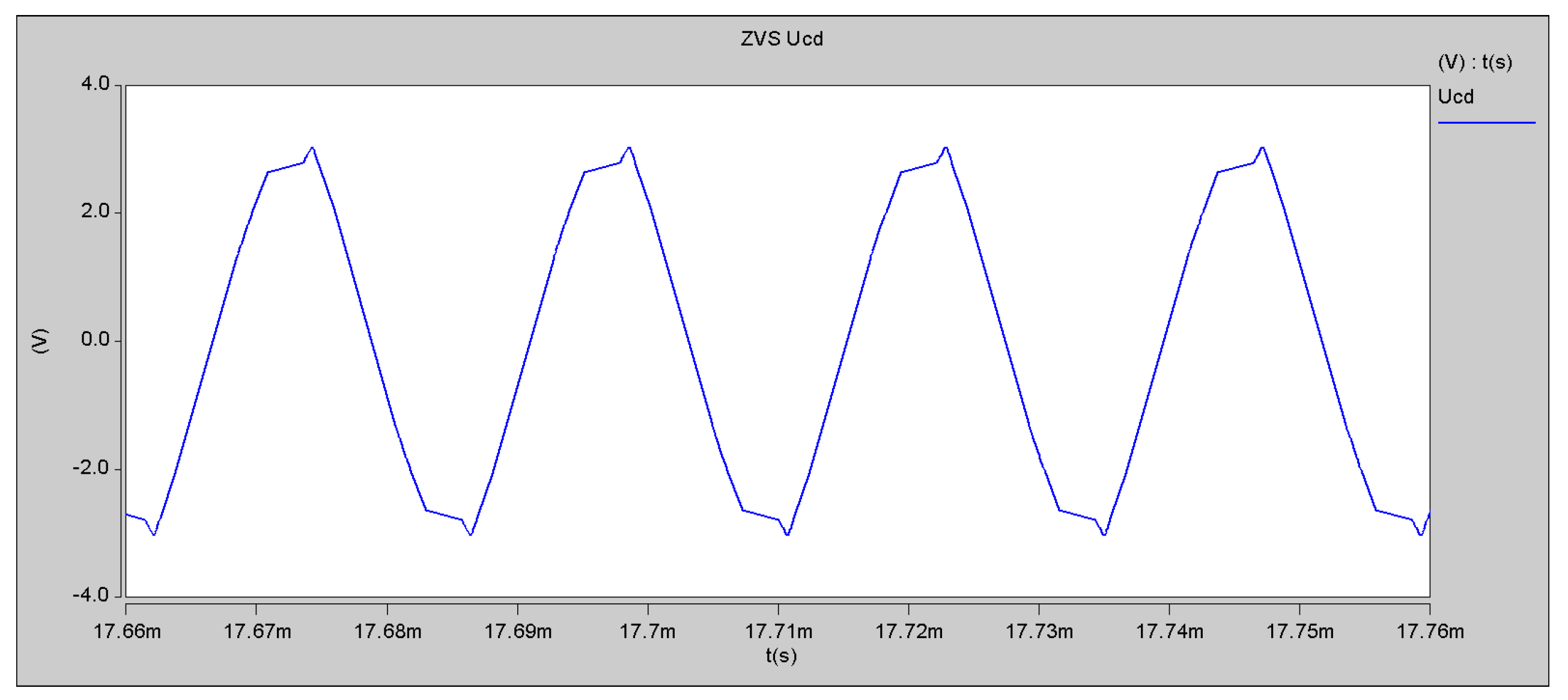
is the voltage difference at the midpoint of the two legs,
is the current at the primary side of the transformer, and
is the voltage at the cathode of the rectifier diodes.
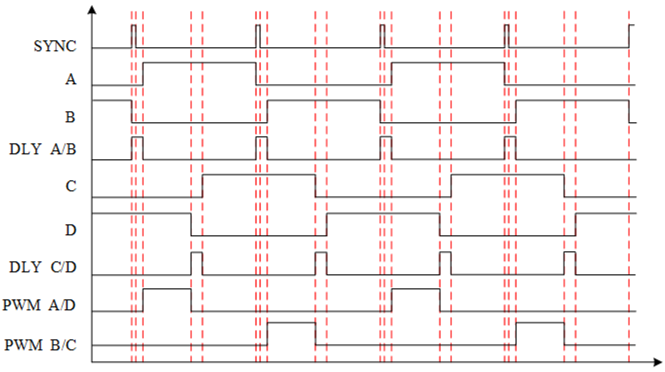
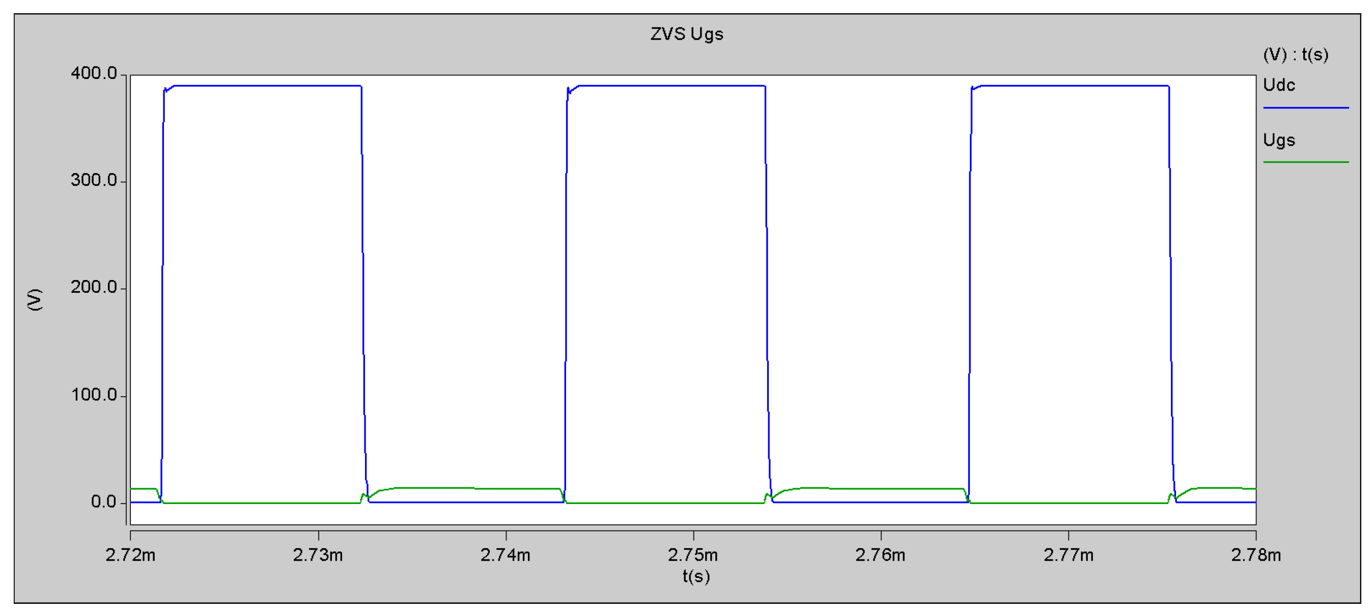
The output terminals A/B and C/D can drive the two legs of Q1/Q2 and Q3/Q4, respectively, and the two legs can independently set the dead time. All pulse width modulation (PWM) duty cycles are close to 50%. When the Q1 and Q4 transistors are turned on at the same time, the current is positive; when the Q2 and Q3 transistors are turned on at the same time, the current is negative. A freely adjustable dead time is set before each output stage. When the Q1 and Q4 transistors cannot be turned on at the same time, the forward current is cut off. Before turning on Q3, due to the dead time setting, the leakage inductance current will continue to flow in the direction of Q2→Q3, which is also the process of C2 and C3 discharging, so that the voltage of Q2 and Q3 transistors sequentially drops to 0, creating conditions for ZVS. The waveform of the control signal of PSFB is shown in
Figure 6.
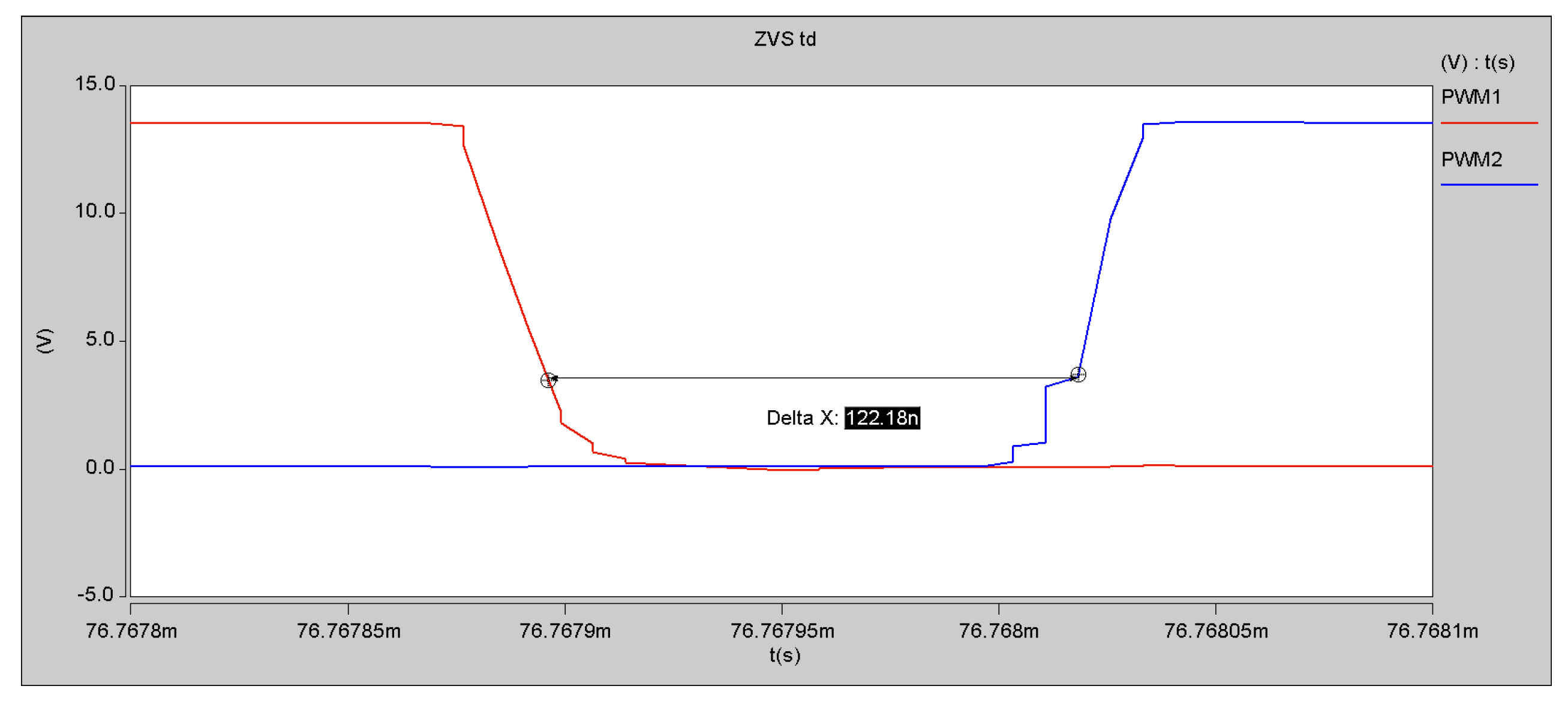
Correct setting of dead time is a necessary condition for the transistor to achieve zero voltage turn-on. The ZVS of the leading leg is determined by the output filter capacitor and transformer leakage inductance, while the lagging leg is determined only by the leakage inductance. The leakage inductance energy is usually small. If its energy is not enough to help the output capacitor of the lagging leg discharge completely, and the primary current reverses in advance, a hard switching phenomenon will occur, and an auxiliary circuit design is required for this. The delay time is
where
is the current value of the first working mode. Dead time is set by adjusting the resistance value of
connected to Pin 15 and Pin 7. In this circuit, take
= 5.1 KΩ, then
This value meets the design requirements. The selected MOSFETS is IRFP460, the turn-off time is 45 ns, and the dead time can ensure the reliable turn-off of MOSFETS. In this paper, L1 = 22 is set by simulation.
2.3. Derating Design at the Component Level
At the component level, we mainly achieve reliability improvement through derating design. The 3 + 1 power supply works at 3/4 of the rated power. When one of the modules fails, the other three modules automatically work at the rated power. In the design process of the power module, special attention should be paid to the components with high power and high heat generation, and the derating design should be carried out for the components with low reliability. Usually, these components are transistors, high-frequency inductors, capacitors, sampling resistors, etc.
- (1)
Transistor parameters
Assuming that the PFC output voltage fluctuates by 5%, the maximum reverse voltage that the power semiconductor switch can withstand is 390 × 1.05 = 409.5 V. Its peak current is:
- (2)
High frequency transformer parameters
The power capacity of the 1000 W, 50 kHz switching power supply is designed as
where
is the apparent power of the transformer, for a full-wave structure transformer, there is
(
P is the input power of the transformer,
is the working efficiency of the transformer, take 0.95);
f is the switching frequency;
is magnetic induction, to prevent core saturation, the value should be lower than 1/3 of the maximum value of the hysteresis loop. Take 0.12 T here.
J is the current density on the wire, generally not more than 600 A/cm
. Take 350 A/cm
here.
is the window usage coefficient, which is related to the wire diameter and the number of windings, and the typical value is 0.4.
We choose ferrite core EE65, the cross-sectional area of its central column is = 5 cm, the window area is = 4.83 cm, and its capacity is × = 24.15 > 7.34, which is sufficient.
Table 3 lists key component derating design parameters.
2.4. Power Consumption Assessment of Key Components
Semiconductor transistors, power diodes, high-frequency transformers, and filter inductors generate significant heat and they are the weak links in power reliability. The power consumption of the input rectifier bridge, PFC transistor, H bridge, and output rectifier diode are estimated separately below. Grid fluctuations are not considered.
- (1)
Rectifier bridge
The effective value of the rectifier bridge current is
where
is the efficiency of the PFC. The average current value of the rectifier bridge is
Then the power of the rectifier bridge is
where
is the forward voltage drop of the diode.
- (2)
PFC transistor
The PFC switch tube is SPW35N60CFD, and its conduction loss is [
35]
Through manual query, the PFC switch tube rise time
= 25 ns, fall time
= 12 ns, and output capacitance
= 1400 PF. Then the switching loss is
Therefore, the total power consumption of the PFC switch is
- (3)
H bridge
Since the circuit works in the ZVS state, the switching loss is very small and can be ignored. The conduction loss of the H-bridge is proportional to the duty cycle, and its maximum conduction loss is
- (4)
Output rectifier diode
Diode losses mainly include conduction loss
, reverse loss
, and reverse recovery loss
. When outputting 50 V/20A DC in the rated working state, then
where
is the duty cycle of the diode, which is taken as 0.5, and
is the reverse voltage of the diode.
It can be seen that the power consumption of the H bridge is low due to the realization of ZVS. The high power consumption of PFC transistors is one of the obstacles to their application in high-power power supplies. The diode has the highest power dissipation of all components due to its large on resistance (1.85 Ω).


