Article

Analysis and Design of Three-Phase LLC Resonant Converter with Matrix Transformers

Department of Electronic and Computer Engineering, National Taiwan University of Science and Technology, Taipei 10607, Taiwan
*
Author to whom correspondence should be addressed.
Energies 2022, 15(4), 1315; https://doi.org/10.3390/en15041315
Submission received: 30 December 2021 / Revised: 3 February 2022 / Accepted: 8 February 2022 / Published: 11 February 2022

Abstract

:
This study presents the topology of a three-phase LLC resonant converter with matrix transformers. The three-phase LLC resonant converter has the advantages of conventional LLC resonant converters, including zero-voltage switching at the primary side, zero-current switching at the secondary side, high-frequency feasibility, and high efficiency. Moreover, it has additional advantages that differ from conventional LLC, including low output capacitor current ripple, natural current sharing in three resonant currents, and a high power level. As a result of the above mentioned characteristics, LLC topology has been used in many electric vehicle charging systems, server power systems, and other high-power applications. However, as the power level becomes higher and higher, the input voltage is usually too high to reduce conduction loss, and the output current also increases. This situation makes transformer design more difficult. The increasing current means more core and copper loss, and the heat dissipation of the transformer becomes more difficult. Matrix transformer technology can improve this problem directly and simply. By utilizing matrix transformers, which are primary series connected and secondary parallel connected, the primary voltage stress and secondary current stress of the transformers can be reduced, and the output current can be distributed. The analysis of the proposed converter in this study includes a circuit operation introduction, a time-domain analysis, calculation of the transfer ratio curve in the frequency domain, and a loss analysis. The theoretical analysis and performance of the proposed converter are verified. A three-phase LLC resonant converter with matrix transformers prototype is built with a high input voltage of 800-VDC and high output current of 200-A. The output voltage is 100-VDC. The waveform and efficiency data will be shown in the experimental results.

1. Introduction

LLC topology has developed rapidly in recent decades. The applications are becoming increasingly extensive [1,2,3,4,5]. From the server power supply to the wireless charger to the electric vehicle charger, the applications are pervasive. The applied power level has increased from hundreds of watts to tens of kilowatts. Faced with increasing demand, LLC topology is still developing. For example, interleaved LLC improves the power level, but the problem of an unbalanced resonant current exists [6,7,8]. The three-phase LLC improves power level further while still maintaining the benefits, such as zero-voltage switching and high efficiency, and also improves disadvantages, such as a high output ripple current and unbalanced current. In addition, different transformer connection methods can lead to different circuit characteristics [9,10,11]. In general, the three-phase LLC has two types of transformer connections: one is Y-connection, and the other is Δ-connection. Y-connection such as Figure 1 is suitable for high-voltage applications, and Δ-connection is suitable for high-current places [12].
To increase the output power level further, this study proposes matrix transformer technology. Matrix transformers with different connection methods can disperse the stress of power components, improve heat dissipation problems, and increase the power level. When working with two transformers, there are four types of different connections that can improve different problems, such as series–series, series–parallel, parallel–parallel, and parallel–series connections [13,14,15,16]. Where [13] and [14] use two transformers to improve the power level, [15] uses a series–series connection to reduce the voltage stress of the transformers and ensure the currents are balanced on the primary side. The authors of [16] use a series–parallel connection to reduce the turns of the primary windings and current stress on the secondary windings. In addition, the conduction loss of rectifier diodes is also reduced. The authors of [17] use a parallel–series connection to achieve a very high step-up ratio (up to 650) as well as high voltage operation (~2-kV). In [18,19], the authors use parallel–series connections to improve performance by reducing the turns of primary windings, decreasing the loss of coils, and reducing cross-regulation problems. In addition to the above voltage/current stress and power level effects, the matrix transformer can be used in planar transformers to improve circuit performance. In papers [20,21], matrix transformers were used to increase the possibilities of the circuit. With integrated transformer technology and advances in high-frequency technology, these two studies not only achieve a high step-down voltage and high efficiency, but also promote switching frequency to 1-MHz. Moreover, the matrix transformer method can be applied to many topologies, for example, the LLC converter [22], AC–DC inverter [23] and flyback converter [24]. The height of double transformers can also be reduced to facilitate occasions with height restrictions. In brief, a series/parallel connection can reduce the voltage/current stress of transformers, and more importantly, matrix transformers can increase the possibilities of the circuit. This study combines double-transformer technology and three-phase Y–Y LLC topology to verify and realize the above advantages.
For the analysis of the three-phase LLC resonant converter with matrix transformers, this paper will first introduce the composition of the proposed converter, then use a frequency-domain analysis to derive the curve of the voltage transfer ratio of the proposed converter. Next, it will introduce the operation principle, a time-domain analysis of different operating states, and a control block diagram. In Section 3, it will provide the components selection and a loss analysis. Finally, the experimental results of the three-phase LLC resonant converter with matrix transformers prototype will be presented. The input voltage is 800-VDC, the output voltage is 100-VDC, and the max output power is 20-kW. The highest efficiency is 97.61%.

2. Three-Phase LLC Resonant Converter with Matrix Transformers

Figure 2 shows the schematic of the three-phase LLC resonant converter with matrix transformers. The topology is composed of three sets of half-bridge LLC. Each half bridge consists of a series resonant tank and a separate set of transformers (T1A and T1B). Three sets of transformers are connected to one another in a Y-type structure at the primary side. Therefore, the voltage stress on the primary side of the transformer is reduced, given the series voltage division, and the current stress on the secondary side is halved because of the parallel connection. Given the reduction of voltage and current stress, transformers and rectifier diodes will have more flexible choices. The heat dissipation capacity is also good.
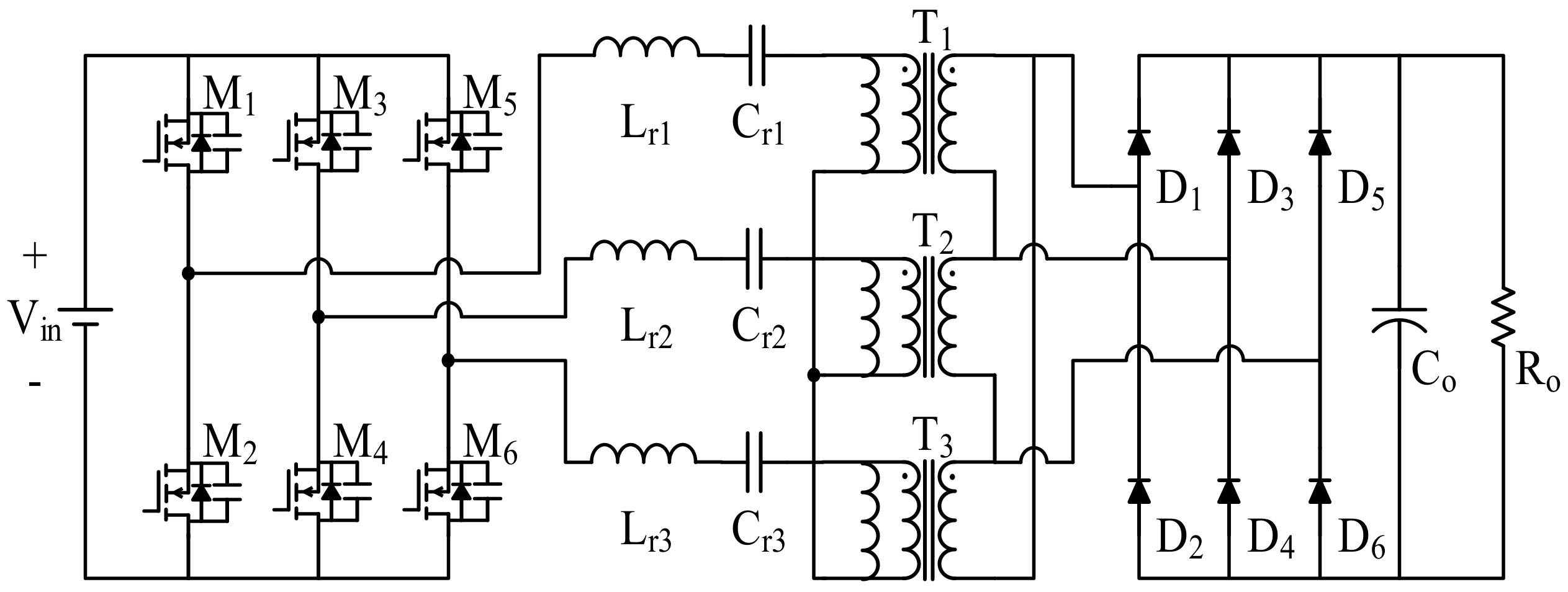
The common point N of Y-connected matrix transformers should be floating. The turns ratio of all transformers is n:1. Transformers TA and TB can be freely selected to be connected in parallel or to output individually. The control method is pulse frequency modulation. Each set of half-bridge signals is in 120° phase shift, and each duty cycle is almost 50%.
This section will provide an analysis of the voltage transfer ratio by using a first harmonic analysis (FHA) of the proposed converter and will introduce circuit operation in different states (regions 1 and 2) and a time-domain analysis. Where Region 1 is the region in which the switching frequency is higher than the first frequency f r 1 , Region 2 is the region in which the switching frequency is lower than the first frequency f r 1 . Circuit analysis is complicated, and thus simplifying the analysis is necessary. The following are our assumptions:
  • The parasitic capacitance of the MOSFET is neglected.
  • Output capacitance C o is large enough so that the output voltage is a constant value.
  • All components are ideal such that the conduction losses of all switches and diodes are neglected.

2.1. Calculation of Voltage Transfer Ratio Curve by FHA

This study uses the FHA method to derive the curve of the voltage transfer ratio. The transfer ratio ( G = n V o V i n ) can be derived by calculating the relationship between the voltage and the current in the first harmonic type and the one cycle. Figure 3 is the single-phase schematic of the proposed converter. The transfer ratio G can be redefined as (1).
G = V o V i n = V o I o I o I A I A V a N V a N V A N V A N V i n
The separate calculation results of (1) are listed in Table 1. All results are presented with the FHA coefficient.
All calculation results are multiplied to obtain the voltage transfer ratio G .
G = H j ω 2 n
The frequency response H j ω can be depicted as Figure 4 and Figure 5. The definitions of all signs are as follows:
  • Frequency response H j ω = 1 ω 1 2 ω 2 2 ω 1 2 ω 2 1 K 2 + Q ω ω 1 ω 1 ω 2
  • Switching angular frequency ω = 2 π f
  • First resonant angular frequency ω 1 = 2 π f r 1
  • Second resonant angular frequency ω 2 = 2 π f r 2
  • Quality factor value Q = L r / C r n 2 R o
  • Ratio of magnetizing inductance to resonant inductance K = L m L r
  • f is switching frequency
  • First resonant frequency f r 1 = 1 2 π L r C r
  • Second resonant frequency f r 2 = 1 2 π L r + L m C r
The condition of Figure 4 is the transfer ratio curve of different Q values under the condition of fixed K = 5, and the condition of Figure 5 is the transfer ratio curve of different K values under the condition of fixed Q = 0.3.
Figure 4 and Figure 5 show that the operate condition depends on the switching frequency and slope of the transfer ratio curve. If the circuit operates at the positive slope, it will be inductive; otherwise, it will be capacitive. If the switching frequency operates at higher than f r 1 (Region 1), the magnetizing inductor will be clamped in all conditions and will not participate in resonance. If the switching frequency operates lower than the f r 2 (Region 2) and positive slope, the magnetizing inductor will decouple in specific stages and participate in resonance. The next section will introduce the operation principle of the two regions.

2.2. Operation Principle and Time Domain Analysis of the Three-Phase LLC Resonant Converter with Matrix Transformers

The operation waveforms of the three-phase LLC resonant converter with matrix transformers in Region 1 are shown in Figure 6. Among them, vgsM1~vgsM6 are control signals of six MOSFETs M1~M6. iLr1, iLr2, and iLr3 are the resonant inductor current. iLm1A, iLm2A, and iLm3A are the magnetizing inductor current. i1A, i2A, and i3A are the transformer secondary current. iD1A, iD2A, iD1B, and iD2B are the rectifier diodes current. The above waveforms definitions can be found in Figure 2. The operation stage in a cycle can be divided into 12 parts (t0~t12). Given that the positive and negative cycles are symmetrical, only the positive cycle will be explained.
Moreover, for the mathematical expression of the resonant tank, the following definitions are required:
Z o = L r C r , Z o is the characteristic impedance.
The statement diagram of each stage is shown in Figure 6.
Stage 1 (t0t1):
As shown in Figure 7a, switches M4 and M5 are turned on and switches M2, M3, and M6 are turned off. Given the continuity of the resonant current i L r 1 , the body diode of switch M1 is turned on. Voltage v A N changes to 1 3 V i n from 1 3 V i n and v a N is 2 3 n V o . The current value i 1 A drops quickly to 0, and then this stage ends. In Region 1, all transformers transfer energy to the secondary side. The resonant inductor current i L r 1 , the resonant capacitor voltage v C r 1 , and the magnetizing inductor current i L m 1 A are shown as follows:
i L r 1 t = i L r t 0 cos ω t t 0 + 1 3 V i n + 2 3 n V o v C r t 0 Z o sin ω t t 0
v C r 1 t = Z o i L r t 0 sin ω t t 0 1 3 V i n + 2 3 n V o v C r t 0 cos ω t t 0 + 1 3 V i n + 2 3 n V o
i L m 1 A t = i L m 1 A t 0 1 3 n V o L m 1 A t t 0
Stage 2 (t1t2):
In this stage, switches M4 and M5 keep turning on, and switches M2, M3, and M6 keep turning off. Switch M1 will turn on after dead time. The current i 1 A drops to 0 and turns to the positive current of Stage 1. Voltage v a N changes to 2 3 n V o . The resonant inductor current i L r 1 , the resonant capacitor voltage v C r 1 , and the magnetizing inductor current i L m 1 A are shown as follows:
i L r 1 t = i L r t 1 cos ω t t 1 + 1 3 V i n 2 3 n V o v C r t 1 Z o sin ω t t 1
v C r 1 t = Z o i L r t 1 sin ω t t 1 1 3 V i n 2 3 n V o v C r t 1 cos ω t t 1 + 1 3 V i n 2 3 n V o
i L m 1 A t = i L m 1 A t 1 + 1 3 n V o L m 1 A t t 1
Stage 3 (t2t3):
As shown in Figure 7c, switches M1 and M4 are turned on, and switches M2, M3, and M5 are turned off. Given the continuity of the resonant current i L r 3 , the body diode of switch M6 is turned on. Voltage v a N changes to 2 3 V i n from 1 3 V i n , and V a N keeps 2 3 n V o . The current value i 3 A drops quickly to 0, and this stage ends. The resonant inductor current i L r 1 , the resonant capacitor voltage v C r 1 , and the magnetizing inductor current i L m 1 A are shown as follows:
i L r 1 t = i L r t 2 cos ω t t 2 + 2 3 V i n 2 3 n V o v C r t 2 Z o sin ω t t 2
v C r 1 t = Z o i L r t 2 sin ω t t 2 2 3 V i n 2 3 n V o v C r t 2 cos ω t t 2 + 2 3 V i n 2 3 n V o
i L m 1 A t = i L m 1 A t 2 + 1 3 n V o L m 1 A t t 2
Stage 4 (t3t4):
In Stage 4, switches M1 and M4 keep turning on, and switches M2, M3, and M5 keep turning off. Switch M1 turns on after dead time. The current value i 3 A drops to 0 at Stage 3 and turns to negative current at this stage. Voltage v a N changes to 4 3 n V o . The resonant inductor current i L r 1 , the resonant capacitor voltage v C r 1 , and the magnetizing inductor current i L m 1 A are as follows:
i L r 1 t = i L r t 3 cos ω t t 3 + 2 3 V i n 4 3 n V o v C r t 3 Z o sin ω t t 3
v C r 1 t = Z o i L r t 3 sin ω t t 3 2 3 V i n 4 3 n V o v C r t 3 cos ω t t 3 + 2 3 V i n 4 3 n V o
i L m 1 A t = i L m 1 A t 3 + 2 3 n V o L m 1 A t t 3
Stage 5 (t4t5):
Following the same rule as in Stages 1 and 3, switches M1 and M6 are turned on, and switches M2, M4, and M5 are turned off. Given the continuity of the resonant current i L r 2 , the body diode of switch M3 is turned on. Voltage v A N changes to 1 3 V i n from 2 3 V i n , and voltage v a N keeps 4 3 n V o . The current value i 2 A drops quickly to 0, and this stage ends. The resonant inductor current i L r 1 , the resonant capacitor voltage v C r 1 , and the magnetizing inductor current i L m 1 A are as follows:
i L r 1 t = i L r t 4 cos ω t t 4 + 1 3 V i n 4 3 n V o v C r t 4 Z o sin ω t t 4
v C r 1 t = Z o i L r t 4 sin ω t t 4 1 3 V i n 4 3 n V o v C r t 4 cos ω t t 4 + 1 3 V i n 4 3 n V o
i L m 1 A t = i L m 1 A t 4 + 2 3 n V o L m 1 A t t 4
Stage 6 (t5t6):
In Stage 6, switches M1 and M6 keep turning on, and switches M2, M4, and M5 keep turning off. Switch M3 turns on after dead time. The current value i 2 A drops to 0 at Stage 5 and turns to positive current at this stage. Voltage v a N changes to 2 3 n V o . The resonant inductor current i L r 1 , the resonant capacitor voltage v C r 1 , and the magnetizing inductor current i L m 1 A are as follows:
i L r 1 t = i L r t 5 cos ω t t 5 + 1 3 V i n 2 3 n V o v C r t 5 Z o sin ω t t 5
v C r 1 t = Z o i L r t 5 sin ω t t 5 1 3 V i n 2 3 n V o v C r t 5 cos ω t t 5 + 1 3 V i n 2 3 n V o
i L m 1 A t = i L m 1 A t 5 + 1 3 n V o L m 1 A t t 5
Figure 8 shows the operation waveforms of the three-phase LLC resonant converter with matrix transformers in Region 2. The definition of all symbols is the same as Region 1. v x is also the transformer primary voltage similar to v L m . The difference is that when the stage is 1, 3, and 5, voltage v L m is related to output voltage. When the stage is 2, 4, and 6, the transformer is decoupled. Thus, voltage v L m is a variable value.
Stage 1 (t0t1):
As shown in Figure 9a, switches M4 and M5 are turned on, and switches M2, M3, and M6 are turned off. Given the continuity of the resonant current i L r 1 , the body diode of switch M1 is turned on. Voltage v A N changes to 1 3 V i n from 1 3 V i n , and voltage V a N is 2 3 n V o . The current value i 1 A rises from 0, and the current value i 1 B drops to 0; then, this stage ends. In this stage, all transformers transfer energy to the secondary side. The resonant inductor current i L r 1 , the resonant capacitor voltage v C r 1 , and the magnetizing inductor current i L m 1 A are as follows:
i L r 1 t = i L r t 0 cos ω t t 0 + 1 3 V i n + 2 3 n V o v C r t 0 Z o sin ω t t 0
v C r 1 t = Z o i L r t 0 sin ω t t 0 1 3 V i n + 2 3 n V o v C r t 0 cos ω t t 0 + 1 3 V i n + 2 3 n V o
i L m 1 A t = i L m 1 A t 0 1 3 n V o L m 1 A t t 0
Stage 2 (t1t2):
In this stage, switches M1, M4, and M5 keep turning on, and switches M2, M3, and M6 keep turning off. The current value i 3 A keeps 0; thus, transformers T3A and T3B are decoupling. Given the decoupling, the transformer voltage depends on the divided impedance between all resonance tanks and the output load. Voltage v a N is defined as v x t . The resonant inductor current i L r 1 , the resonant capacitor voltage v C r 1 , and magnetizing inductor current i L m 1 A are as follows:
i L r 1 t = i L r t 1 cos ω t t 1 + 1 3 V i n v x t v C r t 1 Z o sin ω t t 1
v C r 1 t = Z o i L r t 1 sin ω t t 1 1 3 V i n v x t v C r t 1 cos ω t t 1 + 1 3 V i n v x t
i L m 1 A t = i L m 1 A t 1 + 1 2 v x t L m 1 A t t 1
Stage 3 (t2t3):
As shown in Figure 9c, switches M1 and M4 are turned on, and switches M2, M3, and M5 are turned off. Given the continuity of the resonant current i L r 3 , the body diode of switch M6 is turned on. Voltage v A N changes to 2 3 V i n from 1 3 V i n , and voltage v a N changes to 4 3 n V o from v x . The current value i 3 A rises from 0, and the current value i 2 A drops to 0; then, this stage ends. In this stage, all transformers transfer energy to the secondary side. The resonant inductor current i L r 1 , the resonant capacitor voltage v C r 1 , and the magnetizing inductor current i L m 1 A are as follows:
i L r 1 t = i L r t 2 cos ω t t 2 + 2 3 V i n 4 3 n V o v C r t 2 Z o sin ω t t 2
v C r 1 t = Z o i L r t 2 sin ω t t 2 2 3 V i n 4 3 n V o v C r t 2 cos ω t t 2 + 2 3 V i n 4 3 n V o
i L m 1 A t = i L m 1 A t 2 + 2 3 n V o L m 1 A t t 2
Stage 4 (t3t4):
In this stage, switches M1, M4, and M6 keep turning on, and switches M2, M3, and M5 keep turning off. The current value i 2 A keeps 0; thus, transformer T2A and T2B are decoupling. Given the decoupling, the transformer voltage depends on the divided impedance between all resonance tanks and the output load. Voltage v a N is defined as v x t . The resonant inductor current i L r 1 , the resonant capacitor voltage v C r 1 , and the magnetizing inductor current i L m 1 A are as follows:
i L r 1 t = i L r t 3 cos ω t t 3 + 2 3 V i n v x t v C r t 3 Z o sin ω t t 3
v C r 1 t = Z o i L r t 3 sin ω t t 3 2 3 V i n v x t v C r t 3 cos ω t t 3 + 2 3 V i n v x t
i L m 1 A t = i L m 1 A t 3 + 1 2 v x t L m 1 A t t 3
Stage 5 (t4t5):
As shown in Figure 9e, switches M1 and M6 are turned on, and switches M2, M4, and M5 are turned off. Given the continuity of the resonant current iLr2, the body diode of switch M3 is turned on. Voltage v A N changes to 1 3 V i n from 2 3 V i n , and voltage v a N changes to 2 3 n V o from v x . The current value i 2 A rises from 0, and the current value i 1 A drops to 0; then, this stage ends. In this stage, all transformers transfer energy to the secondary side. The resonant inductor current i L r 1 , the resonant capacitor voltage v C r 1 , and the magnetizing inductor current i L m 1 A are as follows:
i L r 1 t = i L r t 4 cos ω t t 4 + 1 3 V i n 2 3 n V o v C r t 4 Z o sin ω t t 4
v C r 1 t = Z o i L r t 4 sin ω t t 4 1 3 V i n 2 3 n V o v C r t 4 cos ω t t 4 + 1 3 V i n 2 3 n V o
i L m 1 A t = i L m 1 A t 4 + 1 3 n V o L m 1 A t t 4
Stage 6 (t5t6):
In this stage, switches M1, M3, and M6 keep turning on, and switches M2, M4, and M5 keep turning off. The current value i 1 A keeps 0; thus, transformers T1A and T1B are decoupling. Given the decoupling, the transformer voltage depends on the divided impedance between all resonance tanks and the output load. The voltage v a N is defined as v x t . The resonant inductor current i L r 1 , the resonant capacitor voltage v C r 1 , and the magnetizing inductor current i L m 1 A are shown as follows:
i L r 1 t = i L r t 5 cos ω t t 5 + 1 3 V i n v x t v C r t 5 Z o sin ω t t 5
v C r 1 t = Z o i L r t 5 sin ω t t 5 1 3 V i n v x t v C r t 5 cos ω t t 5 + 1 3 V i n v x t
i L m 1 A t = i L m 1 A t 5 + 1 2 v x t L m 1 A t t 5

2.3. Control Block Diagram

A control block diagram of the three-phase LLC resonant converter with matrix transformers is shown in Figure 10. The control function includes an error amplifier of the PI controller and voltage control oscillator (VCO) for regulated output voltage, and uses the driver IC to isolate the primary and secondary sides.

3. Components Selection and Loss Analysis

Before implementing the experimental circuit, a component selection and loss analysis are necessary. Table 2 is the prototype specification of the three-phase LLC resonant converter with matrix transformers. All component designs and selection are as follows:
The results of the voltage transfer ratio show that the proposed converter and traditional LLC are the same. Therefore, the circuit design and component selection are also similar. Differences are the voltage waveform of the transformers and the utilization of matrix transformers to replace the single transformer. The matrix transformers are series at the primary side and parallel at the secondary side. This kind of composition exists and gains 0.5 times in the circuit. Efficiency is better when operating at the resonance frequency. Thus, the transformer turns ratio can be calculated as follows:
n = V i n 2 V o = 800 2 100 = 4
Figure 11 is the voltage waveform of matrix transformers at the secondary side. Derived from Faraday’s formula, the maximum magnetic flux density B m a x can be expressed as Equation (39).
B m a x = 1 3 V o + 2 3 V o + 1 3 V o 1 6 T s 2 A e N s 10 4 T e s l a = 1 9 V o A e N s f 10 4 T e s l a
After arranging the Equation (39) and plugging the magnetic material data, the minimum secondary turns N s are presented as follows:
N s = 100   V 10 4 9 5.3   c m 40   k H z 0.32   T = 1.638
According to the minimum turns required to be an integer, the number of turns at the secondary side is 2. Therefore, the number of turns at the primary side is 8.
Through simulation, stress analysis loss, analysis, and choice of voltage transfer ratio curve, the component selection results are shown in Table 3. Table 4 provides the voltage/current stress relation formula of the MOSFET and diode. The simulation value is shown in Table 5. The calculation method of loss analysis is shown in Table 6, and the loss ratio distribution diagram is shown in Figure 11. The power components loss analysis includes the MOSFET, diode, transformer, and inductor. The symbols used in the calculation method and material data are described in Table 7.
Figure 12 shows the power loss of the conventional three-phase Y–Y LLC and the three-phase Y–Y LLC with matrix transformers at 50% and 100% load, respectively. The estimation of component loss only includes the MOSFET, diode, transformer, and inductor. The converter with matrix transformer’s total losses at 50% and 100% load are 220-W and 442-W. The estimated efficiency is 97.9% and 97.8%. Results show that the main power loss is the conduction loss of the rectifier diode. The power loss of each rectifier diode and transformer at 100% load is about 24.4-W and 9.1-W. Compare this to the general three-phase Y–Y LLC resonant converter: the power loss of each rectifier diode and transformer at 100% load would be up to about 56.8-W and 22.9-W. This means the matrix transformer method improves efficiency and makes component selection easier.

4. Experimental Results

To verify the feasibility of dual-transformer technology, a 20-kW, input voltage 800-V and output voltage 100-V prototype is built and tested in this study. Figure 13 shows the MOSFET waveform of each low-side signal of the three-phase LLC resonant converter with matrix transformers.
In Figure 13, the phases of each MOSFET are 120° apart from each other. The following data show the waveform from 25% load to 100% load in Figure 14, Figure 15, Figure 16 and Figure 17.
Figure 18 shows the zero voltage turn-on waveform at 25% load. The statement of MOSFET is zero-voltage switching. Figure 19 shows the wave form of the output voltage ripple at 100% load. The output voltage ripple is composed of two parts; one waveform is close to the switching frequency, whereas the other one is a higher frequency, which is caused by MOSFET switching noise. In Figure 19, the peak–peak value of the lower frequency voltage ripple v o is approximately 1 V .
Given that the output transfer ratio is designed at the resonant point, the switching frequency almost does not change from light load to full load. The amplitudes of the three resonant currents are also closed, which means no unbalanced current problem occurs. Figure 20 shows the efficiency of the three-phase LLC resonant converter with matrix transformers. The highest efficiency is 97.61% at 110 A. Full load efficiency is 97.18%. Compared with the prior loss analysis, the experimental results are close to the loss analysis (96.2% at half load and 97.2% at full load). Figure 21 shows the prototype of the proposed converter, and Figure 22 shows the height of the proposed prototype.

5. Conclusions

To increase the output power level of the three-phase LLC resonant converter with matrix transformers, this study proposes dual transformers to replace the original transformer and achieve this purpose. Circuit topology, operation mode, operation principle, time-domain analysis, and frequency analysis are all discussed in the article. It is proposed that this method can reduce transformer voltage/current stress and increase output power while maintaining the advantages of the original topology. Finally, a 20-kW prototype three-phase LLC resonant converter with matrix transformers is built, the experimental results verify the above analysis, and efficiency performance is high.

Author Contributions

Supervision, J.-Y.L.; Writing—Original Draft, Y.-F.L.; Writing—Review, P.-H.L. and H.-Y.Y.; Writing—Review & Editing, Y.-F.L. All authors have read and agreed to the published version of the manuscript.

Funding

This research received no external funding.

Institutional Review Board Statement

Not applicable.

Informed Consent Statement

Not applicable.

Data Availability Statement

Not applicable.

Conflicts of Interest

The authors declare no conflict of interest.

References

  1. Zeng, J.; Zhang, G.; Yu, S.S.; Zhang, B.; Zhang, Y. LLC resonant converter topologies and industrial applications—A review. Chin. J. Electr. Eng. 2020, 6, 73–84. [Google Scholar] [CrossRef]
  2. Musavi, F.; Craciun, M.; Gautam, D.S.; Eberle, W.; Dunford, W.G. An LLC resonant DC–DC converter for wide output voltage range battery charging applications. IEEE Trans. Power Electron. 2013, 28, 5437–5445. [Google Scholar] [CrossRef]
  3. Duan, C.; Bai, H.; Guo, W.; Nie, Z. Design of a 2.5-kW 400/12-V high-efficiency DC/DC converter using a novel synchronous rectification control for electric vehicles. IEEE Trans. Transp. Electrif. 2015, 1, 106–114. [Google Scholar] [CrossRef]
  4. Sun, X.; Shen, Y.; Zhu, Y.; Guo, X. Interleaved boost-integrated LLC resonant converter with fixed-frequency PWM control for renewable energy generation applications. IEEE Trans. Power Electron. 2014, 30, 4312–4326. [Google Scholar] [CrossRef]
  5. Zheng, C.; Chen, B.; Zhang, L.; Chen, R.; Lai, J.S. Design considerations of LLC resonant converter for contactless laptop charger. In Proceedings of the 2015 IEEE Applied Power Electronics Conference and Exposition (APEC), Charlotte, NC, USA, 15–19 March 2015; IEEE: New York, NY, USA, 2015; pp. 3341–3347. [Google Scholar]
  6. Hu, Z.; Qiu, Y.; Wang, L.; Liu, Y.F. An interleaved LLC resonant converter operating at constant switching frequency. IEEE Trans. Power Electron. 2013, 29, 2931–2943. [Google Scholar] [CrossRef]
  7. Xue, B.; Wang, H.; Liang, J.; Cao, Q.; Li, Z. Phase-shift modulated interleaved LLC converter with ultrawide output voltage range. IEEE Trans. Power Electron. 2020, 36, 493–503. [Google Scholar] [CrossRef]
  8. Yu, K.; Du, J.; Ma, H. A novel current sharing method for multi-module LLC resonant converters. In Proceedings of the IECON 2017-43rd Annual Conference of the IEEE Industrial Electronics Society, Beijing, China, 29 October–1 November 2017; IEEE: New York, NY, USA, 2017; pp. 613–618. [Google Scholar]
  9. Arshadi, S.A.; Ordonez, M.; Eberle, W.; Craciun, M.; Botting, C. Three-phase LLC battery charger: Wide regulation and improved light-load operation. IEEE Trans. Power Electron. 2020, 36, 1519–1531. [Google Scholar] [CrossRef]
  10. Rahman, A.N.; Lee, C.Y.; Chiu, H.J.; Hsieh, Y.C. Bidirectional three-phase LLC resonant converter. In Proceedings of the 2018 IEEE Transportation Electrification Conference and Expo, Asia-Pacific (ITEC Asia-Pacific), Bangkok, Thailand, 6–9 June 2018; IEEE: New York, NY, USA, 2018; pp. 1–5. [Google Scholar]
  11. Fei, C.; Gadelrab, R.; Li, Q.; Lee, F.C. High-frequency three-phase interleaved LLC resonant converter with GaN devices and integrated planar magnetics. IEEE J. Emerg. Sel. Top. Power Electron. 2019, 7, 653–663. [Google Scholar] [CrossRef]
  12. Jacobs, J.; Thommes, M.; De Doncker, R.W.A.A. A transformer comparison for three-phase single active bridges. In Proceedings of the 2005 European Conference on Power Electronics and Applications, Dresden, Germany, 11–14 September 2005; IEEE: New York, NY, USA, 2005; p. 10. [Google Scholar]
  13. Lin, B.R.; Yang, W.R.; Chen, J.J.; Huang, C.L.; Yu, M.H. Interleaved LLC series converter with output voltage doubler. In Proceedings of the 2010 International Power Electronics Conference-ECCE ASIA-, Sapporo, Japan, 21–24 June 2010; IEEE: New York, NY, USA, 2010; pp. 92–98. [Google Scholar]
  14. Lin, B.R.; Wu, S.F. Implementation of a series resonant converter with series–parallel transformers. IET Power Electron. 2011, 4, 919–926. [Google Scholar] [CrossRef]
  15. Pittini, R.; Huang, L.; Zhang, Z.; Andersen, M.A. Primary parallel secondary series flyback converter (PPSSFC) with multiple transformers for very high step-up ratio in capacitive load charging applications. In Proceedings of the 2014 IEEE Applied Power Electronics Conference and Exposition-APEC 2014, Fort Worth, TX, USA, 16–20 March 2014; IEEE: New York, NY, USA, 2014; pp. 1440–1447. [Google Scholar]
  16. Kim, H.S.; Jung, J.H.; Baek, J.W.; Kim, H.J. Analysis and design of a multioutput converter using asymmetrical PWM half-bridge flyback converter employing a parallel–series transformer. IEEE Trans. Ind. Electron. 2012, 60, 3115–3125. [Google Scholar]
  17. Lee, S.; Yi, J.; Kim, W.; Cho, B.H. A parallel-series connected four-transformer half bridge DC-DC converter for electric vehicle application. In Proceedings of the 2013 IEEE ECCE Asia Downunder, Melbourne, VIC, Australia, 3–6 June 2013; IEEE: New York, NY, USA, 2013; pp. 711–715. [Google Scholar]
  18. Lin, B.R.; Wu, S.F. ZVS resonant converter with series-connected transformers. IEEE Trans. Ind. Electron. 2010, 58, 3547–3554. [Google Scholar] [CrossRef]
  19. Shen, Y.; Zhao, W.; Chen, Z.; Cai, C. Full-bridge LLC resonant converter with series-parallel connected transformers for electric vehicle on-board charger. IEEE Access 2018, 6, 13490–13500. [Google Scholar] [CrossRef]
  20. Fei, C.; Lee, F.C.; Li, Q. High-efficiency high-power-density LLC converter with an integrated planar matrix transformer for high-output current applications. IEEE Trans. Ind. Electron. 2017, 64, 9072–9082. [Google Scholar] [CrossRef]
  21. Mu, M.; Lee, F.C. Design and optimization of a 380–12 V high-frequency, high-current LLC converter with GaN devices and planar matrix transformers. IEEE J. Emerg. Sel. Top. Power Electron. 2016, 4, 854–862. [Google Scholar]
  22. Mahdizadeh, A.H.; Afjei, E. LLC Resonant Converter Utilizing Parallel-Series Transformers Connection. In Proceedings of the 2019 International Power System Conference (PSC), Tehran, Iran, 9–11 December 2019; IEEE: New York, NY, USA, 2019; pp. 472–477. [Google Scholar]
  23. Meneses, D.; Garcia, O.; Alou, P.; Oliver, J.A.; Prieto, R.; Cobos, J.A. Forward micro-inverter with primary-parallel secondary-series multicore transformer. In Proceedings of the 2014 IEEE Applied Power Electronics Conference and Exposition-APEC 2014, Fort Worth, TX, USA, 16–20 March 2014; IEEE: New York, NY, USA, 2014; pp. 2965–2971. [Google Scholar]
  24. Lo, Y.K.; Lin, J.Y. Active-clamping ZVS flyback converter employing two transformers. IEEE Trans. Power Electron. 2007, 22, 2416–2423. [Google Scholar] [CrossRef]
Figure 1. The conventional three-phase Y–Y connection LLC converter.
Energies 15 01315 g001
Figure 2. Schematic of the proposed three-phase LLC resonant converter with matrix transformers.
Energies 15 01315 g002
Figure 3. Single-phase schematic of the proposed converter.
Energies 15 01315 g003
Figure 4. Relationship between transfer ratio and Q value.
Energies 15 01315 g004
Figure 5. Relationship between transfer ratio and K value.
Energies 15 01315 g005
Figure 6. Operation waveforms of the three-phase LLC resonant converter with matrix transformers in Region 1.
Energies 15 01315 g006
Figure 7. Operation station of the three-phase LLC resonant converter with matrix transformers in Region 1 at (a) Stage 1, (b) Stage 2, (c) Stage 3, (d) Stage 4, (e) Stage 5, and (f) Stage 6.
Energies 15 01315 g007
Figure 8. Operation waveforms of the three-phase LLC resonant converter with matrix transformers in Region 2.
Energies 15 01315 g008
Figure 9. Operation station of the three-phase LLC resonant converter with matrix transformers in Region 2 at (a) Stage 1, (b) Stage 2, (c) Stage 3, (d) Stage 4, (e) Stage 5, and (f) Stage 6.
Energies 15 01315 g009
Figure 10. Control block diagram.
Energies 15 01315 g010
Figure 11. Voltage stress of matrix transformers at secondary side.
Energies 15 01315 g011
Figure 12. Loss ratio distribution at 50% and 100% load.
Energies 15 01315 g012
Figure 13. MOSFET waveform of the proposed converter (Time: 5 µs/div; v g s M 2 : 10 V/div; v g s M 4 : 10 V/div; v g s M 6 : 10 V/div; i L r 3 : 10 A/div).
Energies 15 01315 g013
Figure 14. Operation waveform of the proposed converter at 25% load (Time: 2 µs/div; v g s M 6 : 10 V/div; i L r 1 : 10 A/div; i L r 2 : 10 A/div; i L r 3 : 10 A/div).
Energies 15 01315 g014
Figure 15. Operation waveform of the proposed converter at 50% load (Time: 2 µs/div; v g s M 6 : 10 V/div; i L r 1 : 10 A/div; i L r 2 : 10 A/div; i L r 3 : 10 A/div).
Energies 15 01315 g015
Figure 16. Operation waveform of the proposed converter at 75% load (Time: 2 µs/div; v g s M 6 : 10 V/div; i L r 1 : 10 A/div; i L r 2 : 10 A/div; i L r 3 : 10 A/div).
Energies 15 01315 g016
Figure 17. Operation waveform of the proposed converter at 100% load (Time: 2 µs/div; v g s M 6 : 10 V/div; i L r 1 : 10 A/div; i L r 2 : 10 A/div; i L r 3 : 10 A/div).
Energies 15 01315 g017
Figure 18. Operation waveform of zero-voltage turn on at 25% load (Time: 2.2 µs/div; v g s M 3 : 10 V/div; v d s M 3 : 200 V/div; i L r 3 : 10 A/div).
Energies 15 01315 g018
Figure 19. Operation waveform of output voltage ripple at 100% load (Time: 2.2 µs/div; v g s M 3 : 10 V/div; v d s M 3 : 200 V/div; i L r 3 : 50 A/div; v o _ r i p p l e : 2 V/div).
Energies 15 01315 g019
Figure 20. Efficiency of the three-phase LLC resonant converter with matrix transformers.
Energies 15 01315 g020
Figure 21. Prototype of the three-phase LLC resonant converter with matrix transformers.
Energies 15 01315 g021
Figure 22. Height of the three-phase LLC resonant converter with matrix transformers.
Energies 15 01315 g022
Table 1. Design parameters of the experiment and simulation.
Separate PartCalculation Results
V o I o R o
I o I A 6 n π
I A V a N π 2 24 n 2 R o
V a N V A N H j ω
V A N V i n 2 π
Table 2. Prototype specification.
ItemValue
Input voltage V i n 800 V
Output voltage V o 100 V
Output current I o 200 A
Output power P o 20 kW
Switching frequency40~250 kHz
Table 3. Components list.
ItemValue
MOSFETFF23MR12W1M1_B11
DiodeDSS2x101-02A
Transformer turns ratio4:1
Magnetizing inductor 50   μ H
Resonant inductor 20   μ H
Magnetic material3C95
Table 4. Relation formula of MOSFET and diode stress.
ItemRelation Formula
MOSFETVoltage stress V i n
Current IRMS π 12 I o n
DiodeVoltage stress V o
Average current I o 6
Table 5. Voltage/current stress simulation result of MOSFET and diode.
Item50% Load100% Load
MOSFETVoltage stress800 V800 V
Current IRMS10.09 A15.10 A
DiodeVoltage stress100 V100 V
Average current17.20 A32.20 A
Table 6. Calculation method of loss analysis.
ComponentLoss TypeCalculation Method
MOSFETConduction loss I M O S F E T _ R M S 2 R D S _ O N
Switching loss E o f f f
DiodeConduction loss V f I D i o d e _ A V G
Magnetizing inductorCore loss P c v V e
Copper loss I T r _ p r i _ R M S 2 R p r i + I T r _ s e c _ R M S 2 R s e c
Resonant inductorCore loss P c v V e
Copper loss I L r _ R M S 2 R L r
Table 7. Symbol description.
ItemDescription
I M O S F E T _ R M S RMS current flow across the MOSFET
R D S _ O N Resistance between the drain and source in MOSFET
E o f f Turn-off energy loss per pulse
P c v Core loss volume density
V e Effective core volume
A e Effective cross-sectional area
N s Number of turns
I T r _ p r i _ R M S RMS current flow across the transformer primary side
I T r _ s e c _ R M S RMS current flow across the transformer secondary side
I L r _ R M S RMS current flow across the resonant inductor
R p r i Copper resistance of transformer primary side
R s e c Copper resistance of transformer secondary side
R L r Copper resistance of resonant inductor
Publisher’s Note: MDPI stays neutral with regard to jurisdictional claims in published maps and institutional affiliations.

