Abstract
Ca-doped TiO2 films were synthesized by the modified sol-gel method and employed as the electron transport material of perovskite solar cells (PSCs). Morphological, optoelectronic, thermal, and electrical studies of thin films were investigated through XRD, RAMAN, SEM, AFM, UV-Vis, FTIR, and IV characteristics. Ca doping was detected with the help of structural properties while morphological analysis revealed that thin films based on Ca-doped titania are crack-free, homogenous, and uniformly distributed. Further optoelectronic properties have shown a promising conversion efficiency of 9.79% for 2% Ca-doped titania followed by 1% Ca-doped titania, while 3% have shown the lowest conversion efficiency among these prepared samples. The 2% an optimized doping of Ca has shown an almost two-fold increase in conversion efficiency in comparison to pristine TiO2, along with an increase in current density from 15 mA⋅cm−2 to 19.3 mA⋅cm−2. Improved energy efficiency and higher current density are attributed to faster electron transportation; moreover, the optimized percentage of Ca doping seems to be an effective approach to improve the PSCs’ performance.
1. Introduction
Photovoltaic technology holds great potential to meet the growing demand for energy in the world; however, it contributes only over 2% of the world’s energy output due to the high cost of photovoltaic solar cells [1]. Solar energy is a complement to meeting future energy needs, with various advantages over other renewable and eco-friendly energy sources. Perovskite solar cells (PSCs) have shown rapid and immense enhancement in power conversion efficiency (PCE), majorly attributed to carrier mobility [2]. The PSCs have exceptional optoelectronic properties due to low cost [3], rapid extraction, the transportability of the electron transport layer (ETL), and the electron blocking properties of the hole transport layer (HTL) [4,5,6]. Studies have shown that the engineering of interfaces and contact layers leads to the enhanced photovoltaic performance of PSCs [7]. Therefore, in addition to the high-quality absorber layer such as the wide bandgap [8], the performance of PSCs significantly depends on the choice of ETL, HTL materials, and electrical contacts [9]. N-type ETL in planar PSCs majorly consists of titanium dioxide (TiO2), responsible for suppressing the front surface that leads to recombination and ensuring efficient transport of photo-generated electrons [10]. Many other ETLs have been studied previously and have shown promising performance, such as ZnO, PCBM, and C60. PCBM have shown an enhanced conversion efficiency from 13% to 17% due to the reduction in trap states when spray coated [11]. PCBM/C60 was also used in a study resulting in high charge extraction efficiency [12]. ZnO is another promising candidate that is used as the ETL in perovskite solar cells, and recently doped ZnO has shown the power conversion efficiency of 8.98% [13] due to having similar properties to TiO2; however, TiO2 is extensively studied in PSCs as an ETL and as a front contact in PSC-based tandem solar cells [14]. One of the limitations of the TiO2 ETL is the presence of trap sites leading to carrier accumulation and low conductivity, as observed in DSSCs applications [15]. Therefore, there is a crucial need to enhance its carrier transportability to enhance the overall performance of PSCs.
Various studies have been conducted to enhance the optoelectronic properties [16] of TiO2-based ETLs. For instance, a TiO2/ZnO film was investigated as an ETL layer in planar PSCs with improved morphological as well as optical properties of the ETL, leading to an enhanced performance by suppressing the recombination in the PSCs [17]. Studies have suggested an increase in conductivity and a reduction in the surface defect density is subjected to TiO2 doping with metal and nonmetal, e.g., W, N, Ca2+, etc. [18]. Different metals like Ta [19], Co [20], and Mg [21] have also been reported as potential dopants into TiO2 to tailor its properties as an ETL. Though Ca is used as a dopant for organic electron transport materials [22], in inorganic semiconductors such as TiO2 for PSCs it is yet to be explored and needs intensive exploration to achieve enhanced performance. Recent studies have shown room to improve both the electrical and the optical properties by metal doping in TiO2 that is employed as an ETL for PSCs [23]. Therefore, it can be concluded that metallic dopants such as Ca can improve the performance of TiO2 in PSCs and further investigation is required in this area.
In our current study, Ca-doped TiO2 was prepared by the sol-gel solution method with Ca doping varying from 1% to 3%, which are later used as the ETL for PSCs for the first time. Further, the prepared samples were characterized for structural, morphological, and optoelectronic properties by using X-ray diffraction (XRD), Raman analysis, a scanning electron microscope (SEM), an atomic force microscope (AFM), and the Hall effect. Finally, thin films based on Ca-doped titania and pristine titania were prepared and employed as the ETL in PSCs to investigate the PSCs performance under one sun conditions.
2. Materials and Methods
2.1. Synthesis of TiO2 Sol-Gel
TiO2 sols were prepared by using titanium (IV) tetraisopropoxide (TTIP) (Sigma-Aldrich, St. Louis, MO 63118, USA). Distilled water was mixed and stirred for 1 hr at 60 °C followed by HCl (37% pure), which was added dropwise into the solution to achieve a uniform dispersion. The 0.745 mL (9.07 mmol) of HCl was added into 1.05 mL (5.06 mmol) of TTIP to obtain a pale yellow solution having a pH in the range of 4–6. Here, TTIP was used as a Ti source, and for Ca doping calcium nitrate, (Ca (NO3)2·4H2O) (Sitara Chemical Industries Ltd., Faisalabad, Pakistan) was used. Pristine TiO2 was synthesized by using the sol-gel method, while compositional engineering was employed to obtain Ca-doped TiO2 (Ti1-X CaXO, where x = 0.01 for 1%, 0.02 for 2%, and 0.03 for 3% Ca doping by weight).
2.2. Fabrication of Perovskite Solar Cell
Fluorine-doped tin oxide (FTO) glass substrates (Sigma-Aldrich, USA, sheet resistance 10 Ω/sq) were cleaned in an ultrasonic bath sequentially using distilled water and ethanol (ACS reagent, Washington, DC, USA, 97%). Substrates were then dried using an air stream and were subjected to ultraviolet ozone treatment for 20 min to remove organic materials. For undoped ETL samples, a thin layer of TiO2 (40 nm) was deposited on the FTO substrate using the sol-gel precursor solution containing titanium (IV) isopropoxide (TTIP, 0.12M), ethanol, and HCL (0.12M) by spin coating at 3500 RPM. Deposited film was dried at room temperature and subjected to heat treatment at 450 °C for 1 h. For Ca-doped TiO2 films, calcium nitrate (Ca (NO3)2·4H2O) was used as a dopant. An amount of 1 wt%, 2 wt%, and 3 wt% of Ca (NO3)2⋅4H2O) were added to TTIP, ethanol, and HCL, and spin-coated (SAI IVP250) at 3500 RPM to get 1 wt%, 2 wt%, and 3 wt% Ca-doped TiO2 thin films (40 nm).
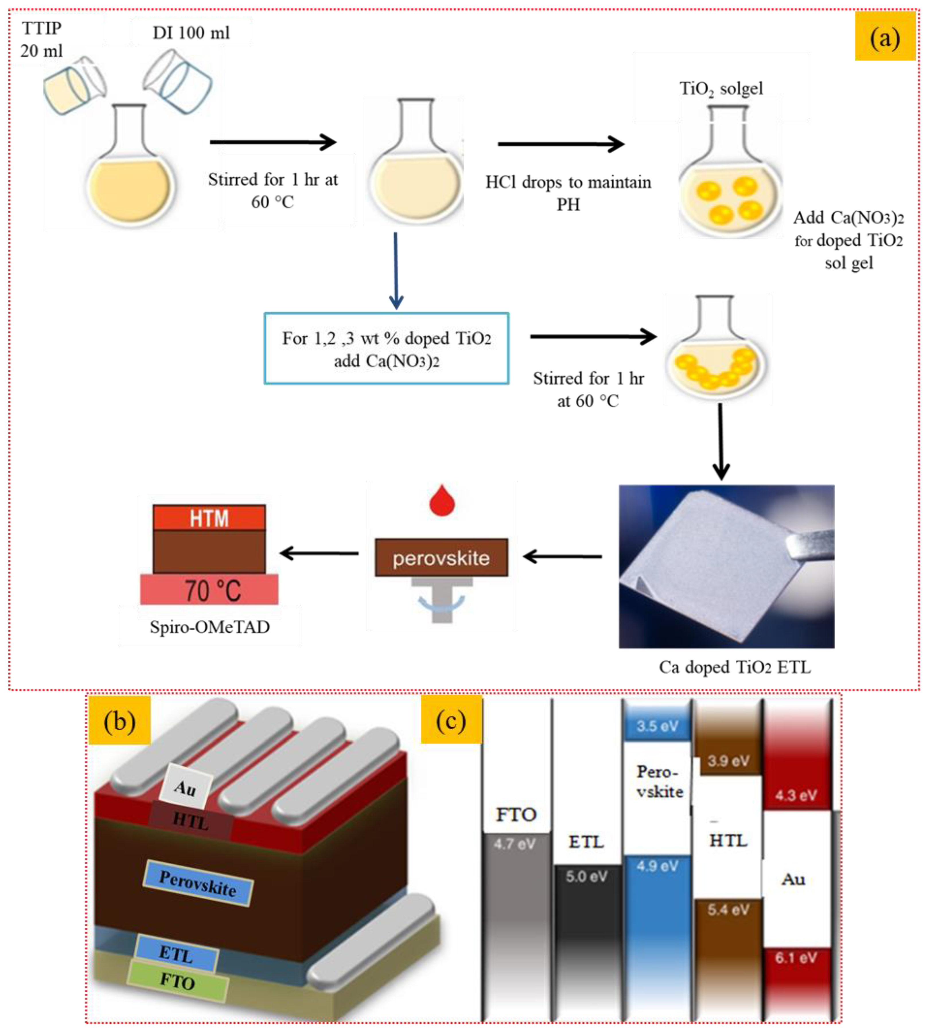
To deposit the perovskite absorber layer, 20 μL of precursor solution containing lead bromide (PbBr2) (Sigma-Aldrich, USA) (0.2 mM), formamidinium iodide (FAI) (Sigma-Aldrich, USA) (1 mM), methylammonium bromide (MABr) (Sigma-Aldrich, USA, 0.2 mM), and lead iodide (PbI2) (1.1 mM) dissolved in dimethylformamide (DMF) (ACS Reagent, 0.8 mL) and 0.2 mL dimethyl sulfoxide (DMSO) (ACS, USA, 0.2 mL) was spin-coated on prepared doped and undoped ETL layers at 4500 rpm for 7 s. To initiate crystallization of the perovskite layer. A total of 90 μL of anhydrous chlorobenzene (Sigma-Aldrich, USA) was dropped while the substrate continued the spinning for 10 s and was finally dried on a hot plate for 15 min at 100 °C. To deposit the HTL layer (350 nm), precursor solution containing spiro-OMeTAD (100 mg) and chlorobenzene (1.094 mL) was spin-coated on the absorber layer at 2000 rpm for 20 s. The perovskite layer and HTL were fabricated inside an N2-filled glove box. The thermal evaporator was used to deposit gold back electrodes (80 nm) under a vacuum of 10−7 Torr. The complete sol-gel process for the formation of the undoped and Ca-doped TiO2 thin films and spin-coating deposition is explained in Figure 1a. Schematic of the fabrication of the perovskite solar cell as a device architecture is presented in Figure 1b,c.
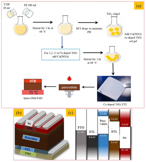
Figure 1.
Sol-gel formation and thin film deposition of Ca-doped TiO2 thin films; (a) synthesis of doped and undoped TiO2 and perovskite solar cell fabrication (b,c) Schematic of perovskite solar cell fabrication.
2.3. Material Characterizations
To determine the structural properties and to check the effect of the Ca-TiO2 structure, XRD analysis was characterized by D8 Advance (Bruker Advanced, Berlin, Germany) [24] and a radiation wavelength of 1.5418 Å in the range of 2θ = 10° to 80° with a step size of 0.05°/5 s. MDI Jade 6.5 software was used to investigate the crystallinity. Further crystallite size, microstrain, and dislocation density were calculated by using the Sherrer’s equation and Williamson and Smallman’s relation, as presented in the following Equations (1)–(3) [25,26,27,28].
where D is an average crystallite size and β is the full width at half maxima (FWHM) of (101) peak.
To support the structural analysis and phase composition, Raman spectroscopy was performed using a Raman spectroscope (RENISHAW Invia 2000, Gloucestershire, UK) with an argon laser emitting a power of 514 nm.
Moreover, to examine the morphology and surface analysis of the thin films were examined using scanning electron microscopy (SEM) (JEOL JSM6490A, Tokyo, Japan) with an accelerating voltage of 20kV, and the gold coating was done on all the samples to avoid self-charge generation [29]. For the surface roughness and topography of the thin films, analysis was performed with an atomic force microscope (JEOL SPM5200l, Tokyo, Japan) and operated in ‘tapping mode’.
UV-Vis spectroscopy is used to check the absorbance in the 200 nm–800 nm wavelength range by using the UH4150AD UV-Vis-NIR (Agilent Technologies, Santa Clara, CA, USA).
2.4. Electrical Characteristics Testing
Hall effect system 5300G (Abet Technologies, Inc., Milford, CT, USA) was used to measure the resistivity, conductivity, sheet resistance, and sheet carrier mobility. Measurements were taken under dark conditions and at a temperature of 300 K. Further, the IV characteristics of the fabricated PSC devices for all undoped and doped samples were measured with a solar simulator model Newport 94043A (Abet Technologies, Inc., USA) under 1 sun conditions with a light intensity of 1000 W/m2. The efficiency of the PSC devices was calculated by Equation (4).
In the above Equation (1), η represents the efficiency, Voc is the open-circuit voltage, Jsc is for the short circuit current density, and FF represents the fill factor.
3. Results and Discussion
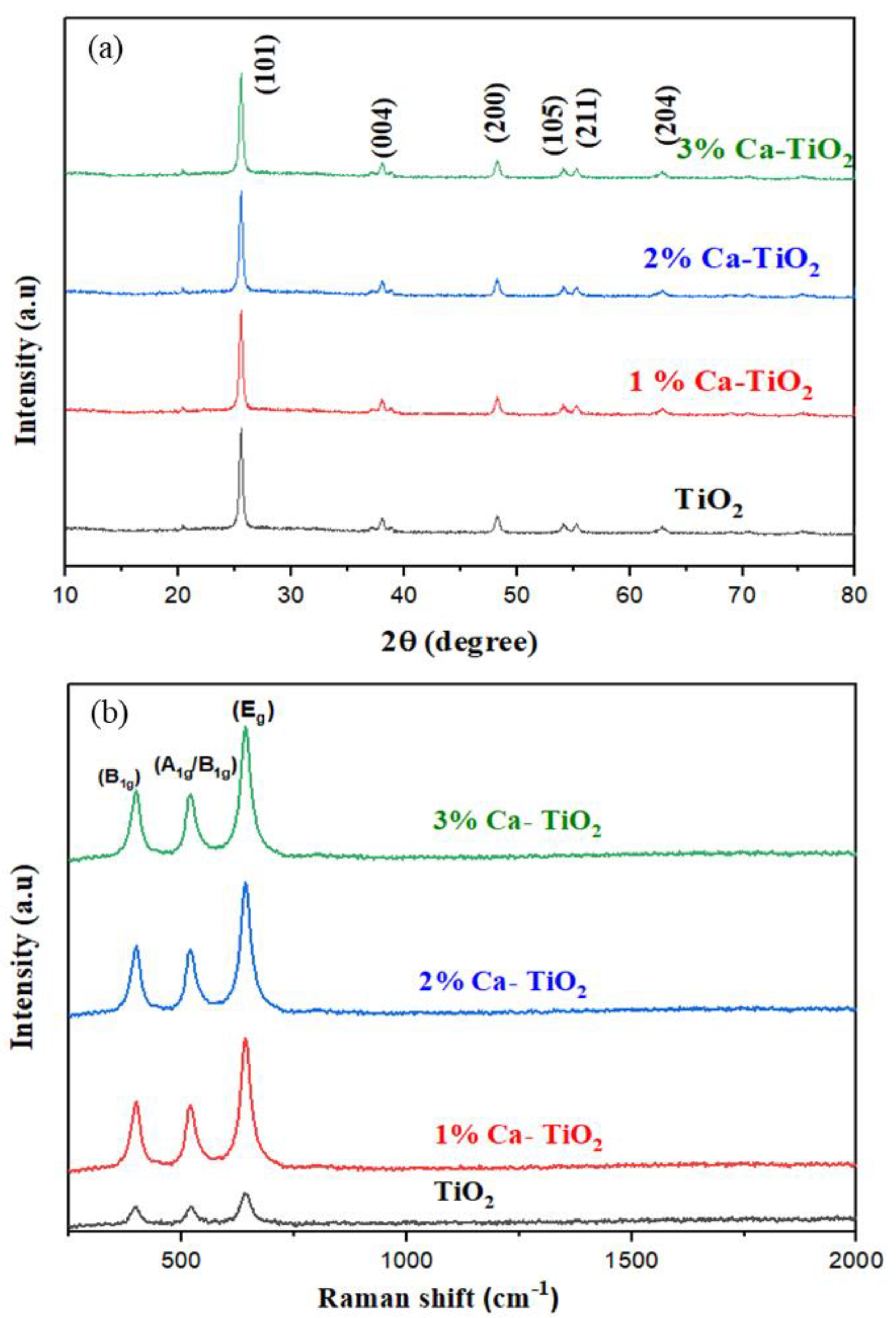
The XRD patterns for the undoped and 1, 2, 3 wt% Ca-TiO2 samples are shown in Figure 2a. The obtained spectra are highly corresponding to the anatase phase titania (JCPDS card no. 21-1272), which has the peaks from (101), (004), (200), (105), (211), and the (204) crystal planes. Major peaks are seen at 2θ = 25.3°, 37.13°, 37.9°, 38.1°, 48.2°, 54.1°, 55.2°, 62.9°, and 68.9° [30]. No extra peak for Ca was observed in the XRD pattern due to the low wt% of the Ca in the doped samples, while the change in the intensity is likely due to the presence of Ca in the titania lattice. The crystallite size of the TiO2, 1 wt% Ca-TiO2, 2 wt% Ca-TiO2, and 3 wt% Ca-TiO2 is 25 nm, 21 nm, 19 nm, and 17 nm, respectively, calculated by using the Scherrer equation [31] that is attributed to Ca doping, which may inhibit the growth of the titania crystallite. As the ionic radius of Ca2+ (0.099 nm) is greater in comparison to Ti4+ (0.068 nm), the Ca2+ ion is doped into a substitutional site of TiO2, resulting in the decrease in the electron density. When the Ca is doped in the substitutional site, it approaches isomorphous substitution. Thus, according to the XRD pattern, the crystal anatase structure was not significantly influenced by the other TiO2 phases or any dopant-induced degradation phases [32].
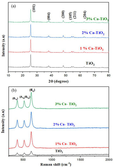
Figure 2.
(a) XRD pattern for undoped TiO2, 1 wt%, 2 wt%, and 3 wt% Ca-doped TiO2; (b) Raman spectra of undoped TiO2, 1 wt%, 2 wt%, and 3 wt% Ca-doped TiO2.
Figure 2b represents the Raman spectra to support the result obtained from the XRD pattern for undoped TiO2 thin films and trace-quantity-doped TiO2 with Ca2+ films in an exciting region of 200–2000 cm−1. The peaks at 246–351 cm−1 are basically due to the O-O covalent interaction. The peaks around the active modes between 144 and 197 cm−1 represent the interaction in the unit cell between Ti–Ti. Raman bands situated at 392, 515, and 633 cm−1 are the notation of B1g, A1g, and Eg anatase phases, respectively. Eg bands appear mainly due to the linear vibration of the O-Ti-O, while the B1g band is due to the fluctuations in the O-Ti-O transition, and the A1g mode is due to the antisymmetric bend vibration of Ti-O-Ti in TiO2 [33]. The main reason is that Ca is present in a much lower concentration, and its inclusion as a dopant in the lattice and its effect is very low given the very weak Raman scattering power. That is why the peaks for Ca oxide are not observed, thus indicating that there are no separate crystalline oxides of Ca, which is well supported by the XRD results. However, a significant change in intensities supports Ca doping. All the peaks show a significant increase in intensities, with an increase in the concentration of Ca that supports the results obtained in the XRD patterns. On the other hand, the decrease in the crystallite size due to the dopant concentration is likely a driver behind the slight shift of the Raman peaks.
Strain analysis and crystallite size was calculated by using Equations (1)–(3) and are presented in Table 1.

Table 1.
Diffraction angle, full wave half maxima, crystallite size, microstrain, and dislocation density of pristine TiO2 1 wt%, 2 wt%, and 3 wt% Ca-doped TiO2.
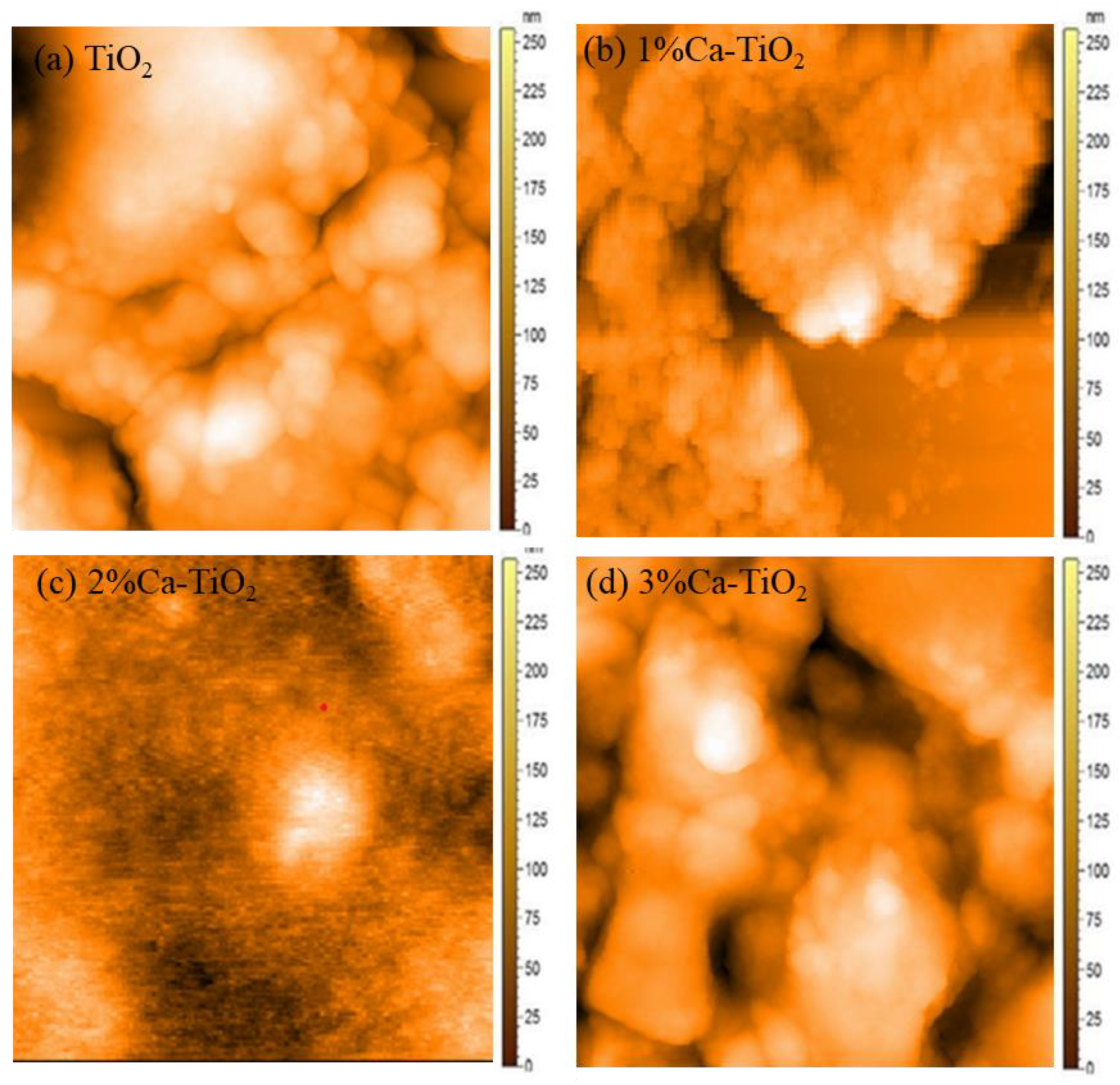
Figure 3a,b demonstrates the SEM micrographs of undoped, 1wt% Ca-doped TiO2 thin films. The TiO2 film deposited demonstrated a smooth surface, while the Ca-doped film showed a slightly porous surface. The micrographs depict the spherical nature of the particles along with the pinhole-free thin films [34]. All the films are quite uniform, crack-free, and also free from agglomeration. Generally, high oxygen pressure favors the formation of the condensed and smooth layer during deposition, since the ablated particles with smaller size after collision with oxygen are advantageous to a homogeneous distribution of the nanostructured layer. This is also mainly due to the anatase in the degenerated phase transition coupled with the growth of the crystals, which leads to the process of external aggregation and coarsening [35]. Such anatase to rutile phase distribution has been widely reported to occur in doped TiO2 films. The cracks conceivably contributed to lateral tension or stress, along with crystal growing.
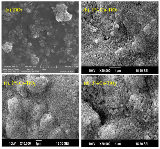
Figure 3.
SEM micrographs of (a) TiO2,1 μm (b) 1% Ca-TiO2, 1 μm (c) 2% Ca-TiO2, 1 μm and (d) 3% Ca-TiO2 1 μm.
Figure 3c,d shows micrographs for 2 wt% and 3 wt% Ca-TiO2 at 1 µm, depicting the additional integration of white matter that appears to be lighter in the micrographs. The accumulation of objects is enhanced by the enhancement of the dopant quantity. This can be described as the formation of doping oxide. Due to this character, the current density factor can also be enhanced, as well as a decrease in the particle size observed in the micrographs. Likely due to the addition of the dopant, the wt% results in decreasing particle size by limiting the growth factor. This decrement in crystallinity is also in agreement with our XRD results. In a previous study, when titania is doped with a dopant to tune the electronic properties, there comes a sufficient decrease in the grain size, consequently decreasing the particle size [36]. Hence, due to the smaller particle size, Ca-doped TiO2 thin films have grown quite uniform, homogenous, and highly dispersed on the surface.
The presence of dopants has a remarkable effect on the morphology of the films. Indeed, all the samples present different textures with uniform and homogenous surface deposition. The surface uniformity of the thin films is disturbed if there is corrosion or the cooling of the sol-gel products. The presence of liquid in the pores during the solvent evaporation can also be responsible for thin film distortion. Because of the fast drying, the spin-coated solution undergoes fast densification. As the solvent decreases, the sol becomes increasingly concentrated, and this is why the viscosity increases, leading to the formation of a rigid nanostructure that later shrinks further due to the tension in the liquid balanced by the compressive forces in the solid phase. Besides, the film is also affected by the tension caused by the oppressive pressure that places it on the rigid substrate. The fabricated films have shown cracks and similar irregularities can be seen in micrographs. The formation of defects may be due to the drying of the material and the difference between the thermal expansion coefficients of the composite film and the bottom layer [37].
Figure 4a shows a 2-D micrograph of pristine TiO2 film and Ca-TiO2. Here, no agglomeration was observed, and pinhole-free films were obtained. Similarly, Figure 4b shows a 2-D micrograph of the 1% Ca-doped TiO2 thin film. Results show some agglomeration but pinhole-free films. Similarly, Figure 4c shows the effects of 2% Ca on the TiO2 2-D thin film. The results revealed the agglomeration at specific points. Moreover, Figure 4d represents the 2-D micrographs of the 3% Ca-doped film. Here, small thick pinholes formed in the film were found along with agglomeration in some areas that can be attributed to the lower PSCs performance. This interaction can also be confirmed from the SEM micrographs, and results in the incorporation of Ca into the TiO2 structure [38]. All the thin films have a thickness in the nanometric range of 40–50 nm, measured by ellipsometry.

Figure 4.
AFM images of (a) TiO2, (b) 1% Ca-TiO2, (c) 2% Ca-TiO2, and (d) 3% Ca-TiO2.
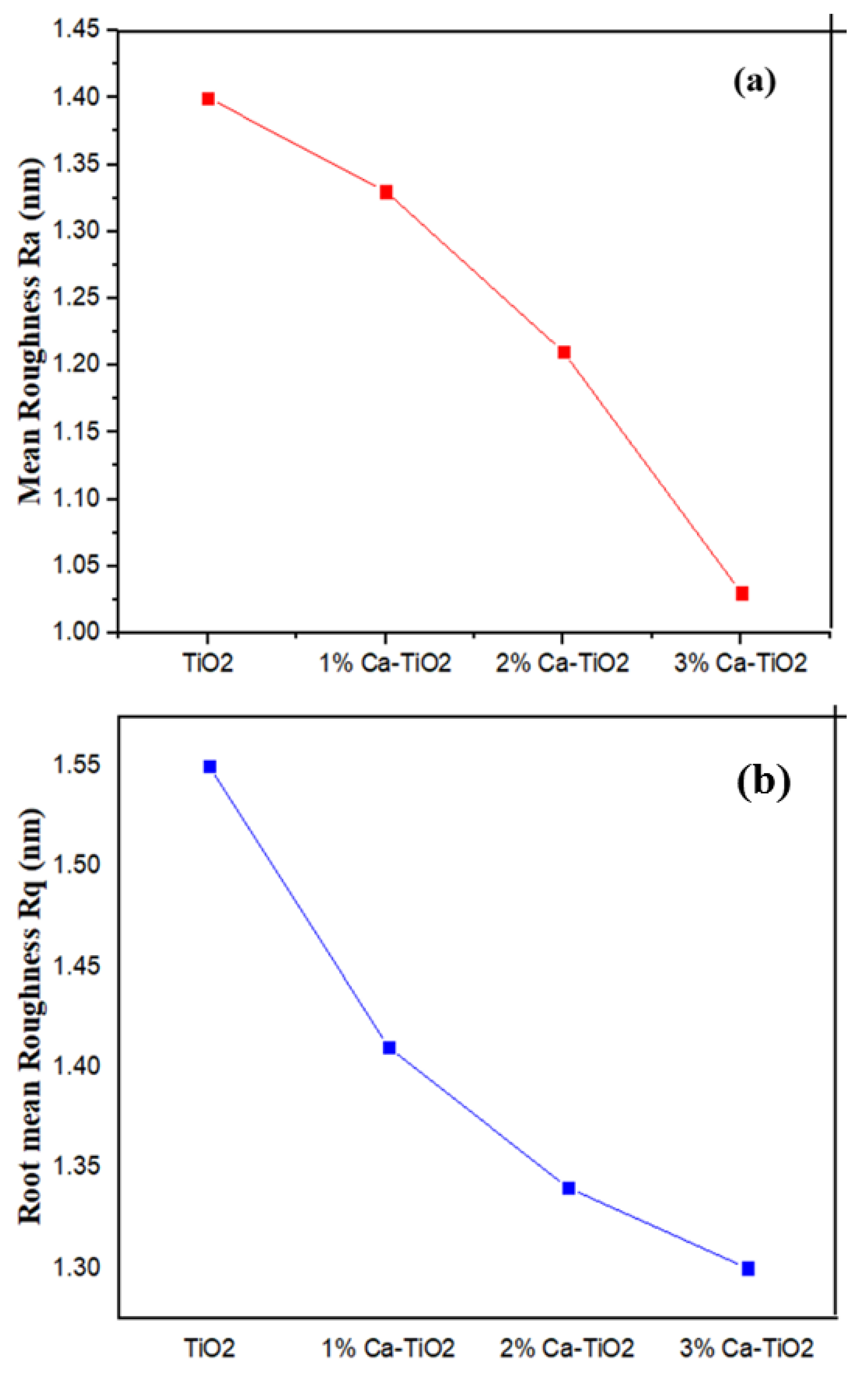
In addition, the roughness parameters (Ra) and the root mean square (Rq) is measured and shown in Figure 5a,b, respectively, and the relative values are shown in Table 2. The roughness for TiO2 is higher as compared to the Ca-doped TiO2 samples. The Ca-doped TiO2 samples demonstrated a continuous decrease in the roughness parameters associated with the increase in the Ca loading [39] that help the uniformity of thin films.
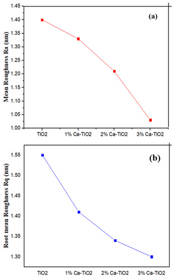
Figure 5.
(a) Mean roughness (Ra) comparison of undoped TiO2, 1 wt%, 2 wt%, and 3 wt% Ca-TiO2 and (b) root mean square roughness (Rq) comparison of undoped TiO2, 1 wt%, 2 wt%, and 3 wt% Ca-TiO2.
Table 2.
Mean roughness (Ra) and root mean square roughness (Rq) of prepared ETL.
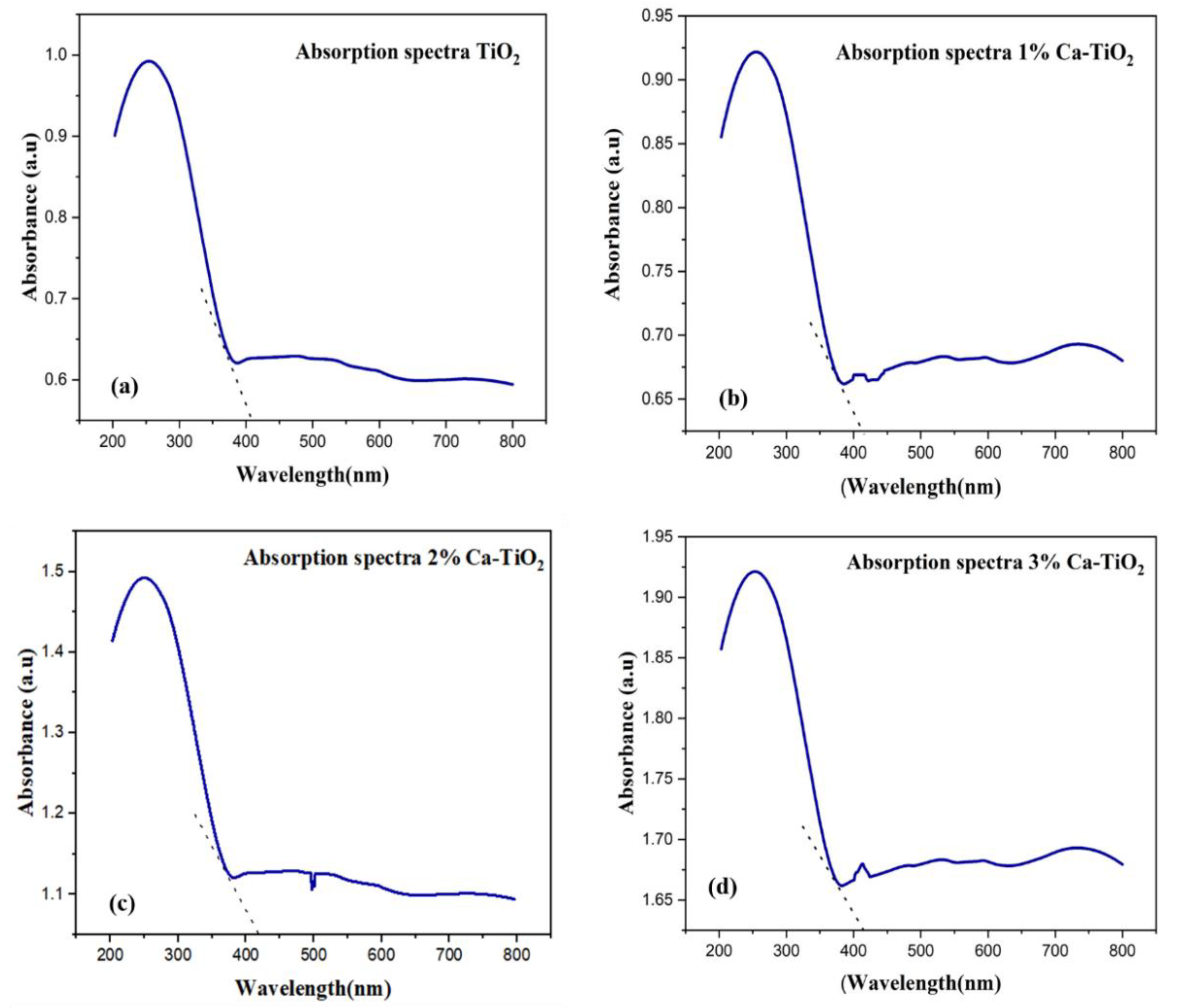
The UV-Vis absorption spectra of undoped TiO2 and Ca-doped TiO2 are presented in Figure 6. Undoped titania shows absorption values lesser as compared to Ca-doped titania, as shown in Figure 6a. For the Ca-doped titania, the absorption values are enhanced, as shown in Figure 6b–d, because of the higher thermodynamic forces which contribute to accelerating more photogenerated electrons from the absorber to the ETL [40]. A redshift is also observed in Figure 6b–d of the Ca-doped titania, which means the absorption range is shifted from the UV range to the visible. Enhanced absorption values in the range of 200–800 nm lead to the formation of another particle transition state for more electronic conduction and an effective reduction of the bandgap on doping, consequently enhancing the photovoltaic performance [41].
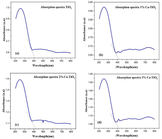
Figure 6.
Absorption (a) TiO2, (b) 1% Ca-TiO2, (c) 2% Ca-TiO2, and (d) 3% Ca-TiO2.
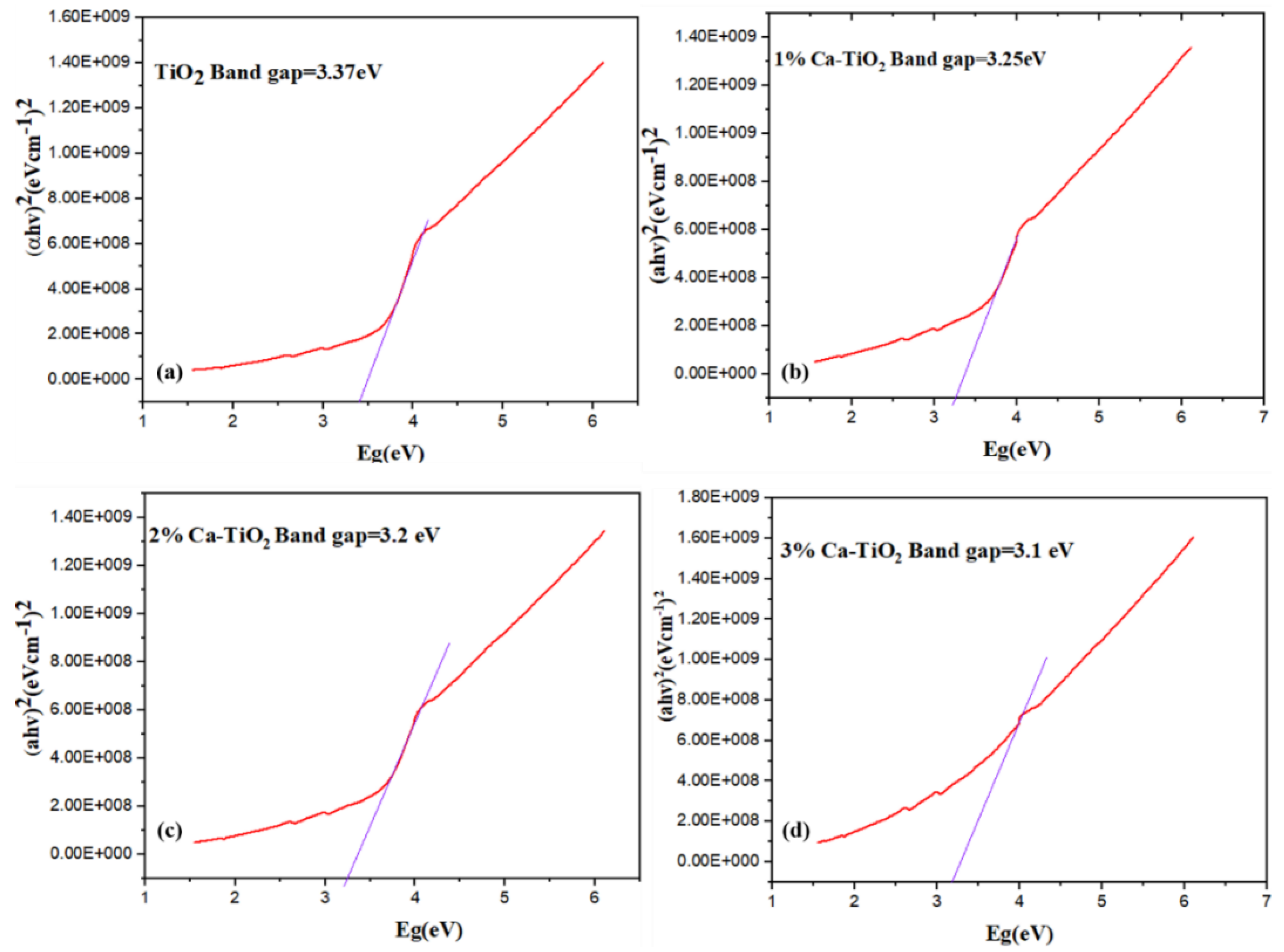
Figure 7a–d represents the Tauc plots for the bandgap calculations [42] of the undoped and doped titania. The bandgap value of the pristine TiO2 is 3.37 eV. In Figure 7b, the bandgap has reduced to 3.25 eV with the effective addition of 1 wt% Ca dopant, attributed to the decreased crystallite size, as discussed in the XRD [43]. In Figure 7c, when 2 wt% Ca is doped, the intermediate states are formed due to the formation of oxides because the Ca and the bandgap values are further reduced up to 3.2 eV. Ca doping also causes the formation of Ti3+, which favors the reduction in the recombination rate of carriers [44]. It is therefore suggested to optimize the Ca2+ substitution into titania, thus resulting in a large number of localized centers and a high conduction of electrons. In Figure 7d, the bandgap value is further reduced to 3.1 eV for 3 wt% Ca-doped titania.
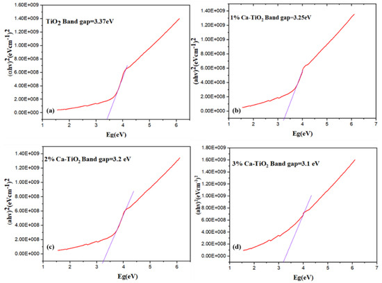
Figure 7.
Tauc plots for bandgap analysis of (a) pristine TiO2, (b) 1 wt% Ca-TiO2, (c) 2 wt% Ca-TiO2, and (d) 3wt % Ca-TiO2.
Table 3 displays the results for the resistivity and conductivity of the thin films based on the pure and doped titania. The pure TiO2 sample showed a high resistivity of 7.28 × 10⁻⁵ Ω cm. The 3% Ca-TiO2 also showed an increase in resistivity, while the 1% and 2% Ca-TiO2 illustrated a significant decrease in resistivity that can be due to the reduced bandgap, as observed in Tauc plot, and a better control on the electronic properties, thus resulting in an enhanced charge extraction and transportation. The increase in resistivity for 3% Ca-TiO2 can be attributed to a significant increase in the thickness, which has an adverse effect on the properties of thin films, especially when dealing in the nanometer ranges [45]. As conductivity is inversely proportional to resistivity, a substantial increase was observed for 1 wt% and 2 wt% Ca-doped titania. Pure titania showed a conductivity of 1.31 × 10⁴ mho-cm, while 1 wt% and 2 wt% showed conductivities of 1.35 × 10⁴ and 1.41 × 10⁴, respectively, which was gradually increased with the increasing dopant. Moreover, the 3 wt% Ca-doped titania showed a decrease in conductivity due to the distortion of the structure and structural instability [46]. Similar to the resistivity and conductivity, the carrier mobility first decreased and then increased as the Ca wt% percentage was increased from 0 (pure TiO2) to 3% [47]. A sharp decrease in the resistance is likely due to the increase in film roughness observed in AFM analysis.
Table 3.
Resistivity, conductivity, and the carrier mobility of all prepared thin films.
For the solar cell parameters, and to check the effect of the Ca tracing amount on the efficiency of the solar cells, J-V measurements were carried out for the undoped titania and the Ca-doped titania ETL-based PSCs, as shown in Figure 8. All the measured parameters are also listed in Table 4. The open circuit voltage is 0.84 V, 0.84, 0.83, and 0.83 V for the pristine titania and 1, 2, and 3 wt% Ca-doped titania, respectively. The current density values jumped from 15.38 mA/cm2 for the pure titania to 19.28 mA/cm2 for the 2 wt% Ca-doped titania due to the higher electronic conduction observed in the Hall effect measurements and the enhanced optical properties observed in the UV-Vis absorption spectra. The further bandgap reduction observed in the Tauc plot can also be responsible for the high electron mobility directly affecting the PSCs’ performance. In addition, the presence of Ca reduces the chances of charge recombination, thereby increasing the photocurrent, [48] possibly due to the diminished oxygen vacancies in the doped samples. In addition, doping may have also helped to decrease the annealing temperature and low temperature processing, and consequently helped to reduce the charge carrier recombination and encouraged the electron extraction, also making it suitable for flexible substrate applications [49]. The solar cell efficiency for 1, 2, and 3 wt% Ca is 9.48, 9.79, and 7.27%, respectively, where 2 wt% of Ca-doped titania indicates the highest efficiency of 9.79%, followed by the 1 wt% Ca-doped titania. While further increasing the dopant amount into the titania, electron trapping sites and grain boundaries formed, resulting in decreased efficiency [50].
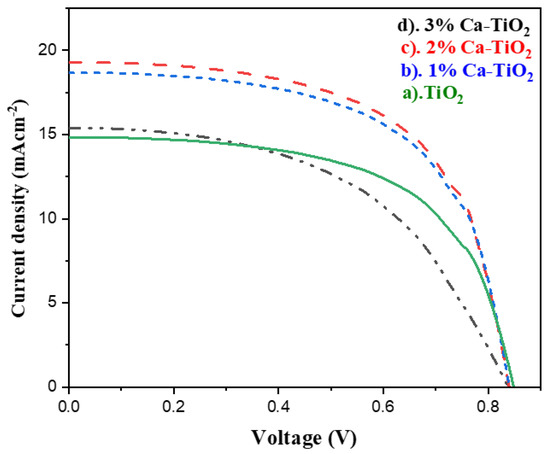
Figure 8.
J-V characteristics of PSCs based on (a) undoped TiO2, (b) 1 wt% Ca doped TiO2, (c) 2 wt% Ca-doped TiO2 photo anodes, and (d) 3 wt% Ca-doped TiO2 photo anode.
Table 4.
PSCS electrical measurements J–V.
Comparison of performance of different metal doped titania based PSCs is presented in Table 5. It is to just comprehend the performance of newly presented material.
Table 5.
Comparison of different metal-doped titania based PSCs’ performance.
4. Conclusions
In summary, different concentrations of Ca-doped TiO2-based thin films were successfully synthesized by employing the sol-gel method and investigated based on their photoelectric properties. The XRD results suggested that Ca-incorporated anatase titania has invariably formed in all the compositions and, more importantly, there is no evidence of secondary or impurity-related peaks detected for all the doped TiO2 samples. The SEM and AFM images revealed that all the thin films were uniform and crack-free with thicknesses in nanometric ranges. The microstructural features of the as-prepared samples were also supported by SEM. The UV-Vis spectroscopy has shown an increase in the absorption with the Ca addition and a simultaneous reduction in the bandgap. The highest conversion efficiency achieved for the 2 wt% Ca-doped titania is 9.79%, followed by the 1 wt% Ca-doped, which is 9.48%, attributed to the higher electronic conduction and the improved optical properties, as well as the enhanced carrier mobility of the optimized doping concentration.
Author Contributions
Conceptualization, A.H.K. and S.S.; methodology, Z.A., A.H.J., S.S. and M.A.; software, A.R. and A.H.J.; validation, A.R., R.J. and S.S.; formal analysis, Z.A., A.H.J. and M.A.; investigation, Z.A., A.H.J. and A.H.K.; resources, R.J. and A.H.K.; data curation, S.F.; writing—original draft preparation, Z.A., A.H.J., S.F., U.Y.Q. and A.H.K.; writing—review and editing, R.J., U.Y.Q., S.S. and A.R.; visualization, A.H.J.; supervision, S.S.; project administration, U.Y.Q. and R.J.; All authors have read and agreed to the published version of the manuscript.
Funding
This research received no external funding.
Institutional Review Board Statement
Not applicable.
Informed Consent Statement
Not applicable.
Data Availability Statement
Not applicable.
Acknowledgments
The authors extend their appreciation to the USPCAS-E NUST for the lab facilities.
Conflicts of Interest
The authors declare no conflict of interest.
References
- Ritchie, H.; Roser, M. Energy, Our World in Data. 2020. Available online: https://ourworldindata.org/energy (accessed on 20 December 2021).
- Valadi, K.; Gharibi, S.; Taheri-Ledari, R.; Akin, S.; Maleki, A.; Shalan, A.E. Metal oxide electron transport materials for perovskite solar cells: A review. Environ. Chem. Lett. 2021, 19, 2185–2207. [Google Scholar] [CrossRef]
- Tariq, M.A.; Shahzad, N.; Sattar, A.; Ahmad, M.; Anwar, M.; Shahzad, M.I. Role of bi-layered CuSCN based hole transport films to realize highly efficient and stable perovskite solar cells. Surf. Interfaces 2022, 28, 101657. [Google Scholar] [CrossRef]
- Yang, G.; Tao, H.; Qin, P.; Ke, W.; Fang, G. Recent progress in electron transport layers for efficient perovskite solar cells. J. Mater. Chem. A 2016, 4, 3970–3990. [Google Scholar] [CrossRef]
- Hossain, M.I.; Hasan, A.K.M.; Qarony, W.; Shahiduzzaman, M.; Islam, M.A.; Ishikawa, Y.; Uraoka, Y.; Amin, N.; Knipp, D.; Akhtaruzzaman, M.; et al. Electrical and Optical Properties of Nickel-Oxide Films for Efficient Perovskite Solar Cells. Small Methods 2020, 4, 2000454. [Google Scholar] [CrossRef]
- Ameer, A.; Shahzad, N.; Tariq, M.A.; Khan, Z.S.; Batool, B.; Haq, S.; Shahzad, M.I. NiO and MWCNT based hole transporting layers for solar cell applications. Bull. Mater. Sci. 2022, 45, 1–9. [Google Scholar] [CrossRef]
- Shadrokh, Z.; Sousani, S.; Gholipour, S.; Abdi, Y. Enhanced photovoltaic performance and stability of perovskite solar cells by interface engineering with poly(4-vinylpyridine) and Cu2ZnSnS4 & CNT. Sol. Energy 2020, 201, 908–915. [Google Scholar] [CrossRef]
- Ahmad, M.; Shahzad, N.; Tariq, M.A.; Sattar, A.; Pugliese, D. Investigating the Sequential Deposition Route for Mixed Cation Mixed Halide Wide Bandgap Perovskite Absorber Layer. Energies 2021, 14, 8401. [Google Scholar] [CrossRef]
- Kanwal, M.; Shahzad, N.; Tariq, M.A.; Shahzad, M.I. Effectively transparent electrical contacts for thermally sensitive solar cells. Sol. Energy Mater. Sol. Cells 2021, 224, 110973. [Google Scholar] [CrossRef]
- Choi, J.; Song, S.; Hörantner, M.T.; Snaith, H.; Park, T. Well-Defined Nanostructured, Single-Crystalline TiO2 Electron Transport Layer for Efficient Planar Perovskite Solar Cells. ACS Nano 2016, 10, 6029–6036. [Google Scholar] [CrossRef]
- Zheng, Y.; Kong, J.; Huang, D.; Shi, W.; McMillon-Brown, L.; Katz, H.E.; Yu, J.; Taylor, A.D. Spray coating of the PCBM electron transport layer significantly improves the efficiency of p-i-n planar perovskite solar cells. Nanoscale 2018, 10, 11342–11348. [Google Scholar] [CrossRef]
- Namkoong, G.; Mamun, A.A.; Ava, T.T. Impact of PCBM/C60 electron transfer layer on charge transports on ordered and disordered perovskite phases and hysteresis-free perovskite solar cells. Org. Electron. 2018, 56, 163–169. [Google Scholar] [CrossRef]
- Park, S.; Kang, R.; Cho, S. Effect of an Al-doped ZnO electron transport layer on the efficiency of inverted bulk heterojunction solar cells. Curr. Appl. Phys. 2020, 20, 172–177. [Google Scholar] [CrossRef]
- Shahiduzzaman, M.; Hossain, M.I.; Visal, S.; Kaneko, T.; Qarony, W.; Umezu, S.; Tomita, K.; Iwamori, S.; Knipp, D.; Tsang, Y.H.; et al. Spray Pyrolyzed TiO2 Embedded Multi-Layer Front Contact Design for High-Efficiency Perovskite Solar Cells. Nano-Micro. Lett. 2021, 13, 1–17. [Google Scholar] [CrossRef] [PubMed]
- Pan, M.; Liu, H.; Yao, Z.; Zhong, X. Enhanced Efficiency of Dye-Sensitized Solar Cells by Trace Amount Ca-Doping in TiO2 Photoelectrodes. J. Nanomater. 2015, 2015, 974161. [Google Scholar] [CrossRef]
- Hossain, M.I.; Shahiduzzaman, M.; Ahmed, S.; Huqe, R.; Qarony, W.; Saleque, A.M.; Akhtaruzzaman, M.; Knipp, D.; Tsang, Y.H.; Taima, T.; et al. Near field control for enhanced photovoltaic performance and photostability in perovskite solar cells. Nano Energy 2021, 89, 106388. [Google Scholar] [CrossRef]
- Fakharuddin, A.; Di Giacomo, F.; Ahmed, I.; Wali, Q.; Brown, T.M.; Jose, R. Role of morphology and crystallinity of nanorod and planar electron transport layers on the performance and long term durability of perovskite solar cells. J. Power Sources 2015, 283, 61–67. [Google Scholar] [CrossRef] [Green Version]
- Castro, Y.; Arconada, N.; Durán, A. Synthesis and photocatalytic characterisation of mesoporous TiO2 films doped with Ca, W and N. Boletín Soc. Española Cerámica Vidr. 2015, 54, 11–20. [Google Scholar] [CrossRef] [Green Version]
- Hsu, C.-H.; Chen, K.-T.; Lin, L.-Y.; Wu, W.-Y.; Liang, L.-S.; Gao, P.; Qiu, Y.; Zhang, X.-Y.; Huang, P.-H.; Lien, S.-Y.; et al. Tantalum-Doped TiO2 Prepared by Atomic Layer Deposition and Its Application in Perovskite Solar Cells. Nanomaterials 2021, 11, 1504. [Google Scholar] [CrossRef]
- Ren, X.; Xie, L.; Bin Kim, W.; Lee, D.G.; Jung, H.S.; Liu, F. Chemical Bath Deposition of Co-Doped TiO2 Electron Transport Layer for Hysteresis-Suppressed High-Efficiency Planar Perovskite Solar Cells. Sol. RRL 2019, 3, 1900176. [Google Scholar] [CrossRef]
- Arshad, Z.; Khoja, A.H.; Shakir, S.; Afzal, A.; Mujtaba, M.A.; Soudagar, M.E.; Fayaz, H.; Farukh, S.; Saeed, M. Magnesium doped TiO2 as an efficient electron transport layer in perovskite solar cells. Case Stud. Therm. Eng. 2021, 26, 101101. [Google Scholar] [CrossRef]
- Shelhammer, D.; Cao, X.; Liu, N.; Wang, H.; Zhou, Y. Doping effects and stability of calcium in organic electron-transport materials. Org. Electron. 2020, 84, 105799. [Google Scholar] [CrossRef]
- Ranjitha, A.; Thambidurai, M.; Shini, F.; Muthukumarasamy, N.; Velauthapillai, D. Effect of doped TiO2 film as electron transport layer for inverted organic solar cell. Mater. Sci. Energy Technol. 2019, 2, 385–388. [Google Scholar] [CrossRef]
- Javed, A.H.; Shahzad, N.; Butt, F.A.; Khan, M.A.; Naeem, N.; Liaquat, R.; Khoja, A.H. Synthesis of bimetallic Co-Ni/ZnO nanoprisms (ZnO-NPr) for hydrogen-rich syngas production via partial oxidation of methane. J. Environ. Chem. Eng. 2021, 9, 106887. [Google Scholar] [CrossRef]
- Musa, M.; Mamat, M.; Vasimalai, N.; Banu, I.S.; Malek, M.; Ahmad, M.; Suriani, A.; Mohamed, A.; Rusop, M. Fabrication and structural properties of flower-like TiO2 nanorod array films grown on glass substrate without FTO layer. Mater. Lett. 2020, 273, 127902. [Google Scholar] [CrossRef]
- Yusoff, M.M.; Mamat, M.H.; Ismail, A.S.; Malek, M.F.; Zoolfakar, A.S.; Suriani, A.B.; Ahmad, M.K.; Nayan, N.; Banu, I.B.S.; Rusop, M. Low-temperature-dependent growth of titanium dioxide nanorod arrays in an improved aqueous chemical growth method for photoelectrochemical ultraviolet sensing. J. Mater. Sci. Mater. Electron. 2019, 30, 1017–1033. [Google Scholar] [CrossRef]
- Yusoff, M.; Mamat, M.; Abdullah, M.; Ismail, A.; Malek, M.; Zoolfakar, A.; Al Junid, S.A.M.; Suriani, A.; Mohamed, A.; Ahmad, M.; et al. Coupling heterostructure of thickness-controlled nickel oxide nanosheets layer and titanium dioxide nanorod arrays via immersion route for self-powered solid-state ultraviolet photosensor applications. Measurement 2020, 149, 106982. [Google Scholar] [CrossRef]
- Yusoff, M.; Mamat, M.; Ismail, A.; Malek, M.; Khusaimi, Z.; Suriani, A.; Mohamed, A.; Ahmad, M.; Rusop, M. Enhancing the performance of self-powered ultraviolet photosensor using rapid aqueous chemical-grown aluminum-doped titanium oxide nanorod arrays as electron transport layer. Thin Solid Film. 2018, 655, 1–12. [Google Scholar] [CrossRef]
- Raza, J.; Khoja, A.H.; Naqvi, S.R.; Mehran, M.T.; Shakir, S.; Liaquat, R.; Ali, G. Methane decomposition for hydrogen production over biomass fly ash-based CeO2 nanowires promoted cobalt catalyst. J. Env. Che. Eng. 2021, 9, 105816. [Google Scholar] [CrossRef]
- Castro, Y.; Durán, A. Ca doping of mesoporous TiO2 films for enhanced photocatalytic efficiency under solar irradiation. J. Sol-Gel Sci. Technol. 2016, 78, 482–491. [Google Scholar] [CrossRef]
- Shakir, S.; Khan, Z.; Ali, A.; Akbar, N.; Musthaq, W. Development of copper doped titania based photoanode and its performance for dye sensitized solar cell applications. J. Alloy. Compd. 2015, 652, 331–340. [Google Scholar] [CrossRef]
- Cheng, X.; Yu, X.; Xing, Z.; Wan, J. Enhanced Photocatalytic Activity of Nitrogen Doped TiO2 Anatase Nano-Particle under Simulated Sunlight Irradiation. Energy Procedia 2012, 16, 598–605. [Google Scholar] [CrossRef] [Green Version]
- Liu, Q. Photovoltaic Performance Improvement of Dye-Sensitized Solar Cells Based on Mg-Doped TiO2 Thin Films. Electrochim. Acta 2014, 129, 459–462. [Google Scholar] [CrossRef]
- Lu, H.; Tian, W.; Gu, B.; Zhu, Y.; Li, L. TiO2 Electron Transport Bilayer for Highly Efficient Planar Perovskite Solar Cell. Small 2017, 13, 1701535. [Google Scholar] [CrossRef] [PubMed]
- Sriubas, M.; Bočkutė, K.; Virbukas, D.; Laukaitis, G. Investigation of the Properties of Ca-doped TiO2 Thin Films Formed by e-beam Evaporation. Procedia Eng. 2014, 98, 133–138. [Google Scholar] [CrossRef] [Green Version]
- Zhang, H.; Shi, J.; Xu, X.; Zhu, L.; Luo, Y.; Li, D.; Meng, Q. Mg-doped TiO2 boosts the efficiency of planar perovskite solar cells to exceed 19%. J. Mater. Chem. A 2016, 4, 15383–15389. [Google Scholar] [CrossRef]
- Istrate, A.-I.; Nastase, F.; Mihalache, I.; Comanescu, F.; Gavrila, R.; Tutunaru, O.; Romanitan, C.; Tucureanu, V.; Nedelcu, M.; Müller, R. Synthesis and characterization of Ca doped ZnO thin films by sol–gel method. J. Sol-Gel Sci. Technol. 2019, 92, 585–597. [Google Scholar] [CrossRef]
- Wang, J.; Yu, J.; Zhu, X.; Kong, X.Z. Preparation of hollow TiO2 nanoparticles through TiO2 deposition on polystyrene latex particles and characterizations of their structure and photocatalytic activity. Nanoscale Res. Lett. 2012, 7, 646. [Google Scholar] [CrossRef] [Green Version]
- Lu, P.-J.; Huang, S.-C.; Chen, Y.-P.; Chiueh, L.-C.; Shih, D.Y.-C. Analysis of titanium dioxide and zinc oxide nanoparticles in cosmetics. J. Food Drug Anal. 2015, 23, 587–594. [Google Scholar] [CrossRef] [Green Version]
- Tang, H.; Prasad, K.; Sanjinès, R.; Schmid, P.E.; Lévy, F. Electrical and optical properties of TiO2 anatase thin films. J. Appl. Phys. 1994, 75, 2042–2047. [Google Scholar] [CrossRef]
- Yang, M. Band Gap Engineering and Carrier Transport in TiO2 for Solar Energy Harvesting. Doctoral Dissertation, University of Pittsburgh, Pittsburgh, PA, USA, 2012. [Google Scholar]
- Javed, A.H.; Shahzad, N.; Khan, M.A.; Ayub, M.; Iqbal, N.; Hassan, M.; Hussain, N.; Rameel, M.I.; Shahzad, M.I. Effect of ZnO nanostructures on the performance of dye sensitized solar cells. Sol. Energy 2021, 230, 492–500. [Google Scholar] [CrossRef]
- Hernandez, J.V. Structural and Morphological Modification of TiO2 Doped Metal Ions and Investigation of Photo-Induced Charge Transfer Processes. Doctoral Dissertation, Université du Maine, Mexico City, Mexico, 2017. [Google Scholar]
- Liu, X.; Bi, Y. Synergistic effect of Ti3+ doping and facet regulation over Ti3+-doped TiO2 nanosheets with enhanced photoreactivity. Catal. Sci. Technol. 2018, 8, 3876–3882. [Google Scholar] [CrossRef]
- Zhang, X.; Stroud, D. Optical and electrical properties of thin films. Phys. Rev. B 1995, 52, 2131. [Google Scholar] [CrossRef] [PubMed]
- Ramaneti, R.; Lodder, J.C.; Jansen, R. Anomalous Hall effect in anatase Co:TiO2 ferromagnetic semiconductor. Appl. Phys. Lett. 2007, 91, 12502. [Google Scholar] [CrossRef] [Green Version]
- Tavakoli, M.M.; Yadav, P.; Tavakoli, R.; Kong, J. Surface engineering of TiO2 ETL for highly efficient and hysteresis-less planar perovskite solar cell (21.4%) with enhanced open-circuit voltage and stability. Adv. Energy Mater. 2018, 8, 1800794. [Google Scholar] [CrossRef]
- Minchi, L.; Cao, F.; Xinni, Z.; Youqiang, C.; Xuhua, L. Photocatalytic activity of Ca-TiO2 nanofibers with different concentrations of calcium. Chem. Phys. Lett. 2019, 736, 136807. [Google Scholar] [CrossRef]
- Shahiduzzaman, M.; Hossain, M.I.; Otani, S.; Wang, L.; Umezu, S.; Kaneko, T.; Iwamori, S.; Tomita, K.; Tsang, Y.H.; Akhtaruzzaman, M.; et al. Low-temperature treated anatase TiO2 nanophotonic-structured contact design for efficient triple-cation perovskite solar cells. Chem. Eng. J. 2021, 426, 131831. [Google Scholar] [CrossRef]
- Liu, Q.; Zhou, Y.; Duan, Y.; Wang, M.; Zhao, X.; Lin, Y. Enhanced conversion efficiency of dye-sensitized titanium dioxide solar cells by Ca-doping. J. Alloy. Compd. 2013, 548, 161–165. [Google Scholar] [CrossRef]
- Teimouri, R.; Heydari, Z.; Ghaziani, M.P.; Madani, M.; Abdy, H.; Kolahdouz, M.; Asl-Soleimani, E. Synthesizing Li doped TiO2 electron transport layers for highly efficient planar perovskite solar cell. Superlattices Microstruct. 2020, 145, 106627. [Google Scholar] [CrossRef]
- Nguyen, T.M.H.; Bark, C.W. Synthesis of Cobalt-Doped TiO2 Based on Metal–Organic Frameworks as an Effective Electron Transport Material in Perovskite Solar Cells. ACS Omega 2020, 5, 2280–2286. [Google Scholar] [CrossRef] [Green Version]


Publisher’s Note: MDPI stays neutral with regard to jurisdictional claims in published maps and institutional affiliations. |
© 2022 by the authors. Licensee MDPI, Basel, Switzerland. This article is an open access article distributed under the terms and conditions of the Creative Commons Attribution (CC BY) license (https://creativecommons.org/licenses/by/4.0/).