Article

Research on Constant Voltage/Current Output of LCC–S Envelope Modulation Wireless Power Transfer System

1
School of Electrical and Electronic Engineering, Chongqing University of Technology, Chongqing 400054, China
2
Energy Internet Engineering Research Center of Chongqing, Chongqing 400054, China
*
Author to whom correspondence should be addressed.
Energies 2022, 15(4), 1562; https://doi.org/10.3390/en15041562
Submission received: 17 December 2021 / Revised: 23 January 2022 / Accepted: 18 February 2022 / Published: 20 February 2022

Abstract

:
As a technology that makes power transfer more flexible, wireless power transfer (WPT) technology has become a hot research topic in recent years. However, most of the existing studies are based on a DC–DC WPT system. If applied to AC loads, the traditional system usually contains multiple energy conversion stages, which lead to a low transmission efficiency and therefore higher costs. Besides, the necessary large electrolytic capacitors make the system unreliable and bulky. The goal of this study is to design a reliable and efficient WPT system featuring constant current (CC) and constant voltage (CV) output for AC loads. In this work, an inductor–capacitor–capacitor series (LCC–S) enveloped modulation wireless power transfer (EM–WPT) system is proposed. The design of the proposed system is elaborated in this paper, including the working principle of the system’s power converters, the relationship between CC/CV output characteristics and the input current, and the control strategy of CC/CV output based on an AC–AC boost converter. Lastly, an experimental prototype is configured to verify the CC/CV characteristics. The measured overall efficiency of the system reaches 91% and the power factor of input power supply approaches 1.

1. Introduction

Wireless power transfer (WPT) technology, as a technology for transmitting power over a large air gap, has attracted the attention of power electronics academia in recent years. Due to the no physical electric connection, it has been used in a wide range of fields such as consumer electronics [1,2], biomedical implant [3], underwater vehicles [4], clean rooms [5], and electric vehicle (EV)charging [6,7,8,9].
Normally, the traditional WPT system consists of multiple power conversion stages, as shown in Figure 1. The first stage, the grid alternating current (AC), is converted to the direct current (DC) bus voltage by a single-phase rectifier. A power factor correction (PFC) circuit is necessary to eliminate power supply current distortion while maintaining a stable DC bus voltage. The next stage is DC–AC inverter, which realizes wireless power transmission by converting low frequency DC to high frequency AC while guaranteeing load requirements and soft switching condition of inverter [10]. An AC–DC rectification stage in the secondary side is used to rectify the induced high-frequency electromagnetic energy into DC electrical energy. The last stage is a DC–DC circuit or a DC–AC inverter as per the power requirements for loads. However, the multiple–stage conversion and the DC–link with large DC electrolytic capacitors can be costly and bulky. Such a system is unreliable, costly, bulky and unreliable because it contains many components [11].
In order to overcome these shortcomings and reduce the number of energy conversion stages, matrix converters based on a wireless power transfer system have been proposed [12]. Nevertheless, matrix converters require complex commutation control. Thus, it is necessary to adopt a simple control strategy of single–stage inductive power transfer (IPT) system to reduce the conversion stages and to increase the system reliability.
In general, the WPT system generates a high frequency current at the primary side through AC–DC–AC power conversion [13,14]. However, additional semiconductor switches, large DC electrolytic capacitors and control circuits may make the system more expensive, bulky and complex [15,16]. A direct AC–AC WPT system based on free oscillation and energy injection control is proposed in [17] to realize the generation of a high–frequency current in the primary coil. The structure of the convertor is simple, but the envelope characteristics of the track current and the design of the pickup are ignored. In addition, an AC–AC converter presented in [18] uses a low energy storage power supply. This technology still retains the AC–DC stage, but it needs to be emphasized that the rectifier is followed by a small filter capacitor to reduce the energy storage of the power supply. This technology can still directly generate a high frequency current at the primary side. In [19] is proposed a single-phase to three–phase converter without a DC link and diode bridge to improve system simplification and efficiency. In [20,21], a cost–effective WPT system for an induction motor was proposed. By using a simple AC chopper as a waveform shaping converter at the secondary side, the ideal AC power can be effectively injected into the motor, and the efficiency of the WPT system is improved by 5%.
The latest research into WPT shows that a single stage direct AC–AC converter can replace the first two power processing stages, namely the UPF rectifier and the high frequency DC–AC inverter [10]. In [22], a three–phase to single–phase matrix converter was proposed, which adopts phase shift modulation for series–compensated WPT converter. The semiconductor switch number that is required in the system is small, and the efficiency of the converter is high. Meanwhile, it is also worth mentioning that there is little research literature in the field of WPT that focuses on the situation of the load demand AC power. Most of the existing research is based on a DC–DC WPT system, such as lithium battery charging. The traditional WPT system uses an additional DC–AC inverter for AC load applications, which will lead to system complexity and cost. Two direct AC WPT systems have been implemented in [23] to realize the independent regulation of the multi–phase AC power supply and loads. There is no need for the power converter in the pick-up side as the AC power of multiple loads can be controlled directly by the system through the transmitter side without any power converter at the receiver side. Nevertheless, this design scheme contains large passive devices, thereby reducing the transmission efficiency and power density of the system. Generally, the motor windings cannot be directly injected by a high frequency AC output current that is produced by the WPT system. In [24], a novel wireless secondary converterless bipolar driver for AC applications is proposed and implemented. Power equalization has been achieved by adopting the inductor–capacitor–inductor (LCL) compensation network; thus two receivers can be served and the low–frequency AC output can be controlled by one transmitter. In the application field of WPT technology, CC mode or CV mode is the most common working mechanism [25]. In recent research, the compensation is very important in reducing the VA rating of the compensation at both sides and the CC/CV charging. In [26], S–LCC, LCC–S and LCC–LCC are compared in detail. Especially, LCC–S compensation topology shows that the WPT system still has a good transmission efficiency in a wide range of load changes [27,28,29,30,31]. Similarly, these studies focus on the DC load (battery charging); little research has been done on AC applications. The main motivation of this paper is to propose an LCC–S Envelope Modulation Wireless Power Transfer System that realizes the CC/CV output for AC applications.
In [32], a magnetic coupling wireless power transmission technology is proposed based on the principle of envelope modulation. It carried out four typical EM–WPT systems. A kind of new AC–DC–AC high frequency convertor based on series resonance is proposed in [14]. A high–frequency current whose amplitude envelope changes regularly in half–waves is modulated in the transmitting coil to realize the wireless transmission of electric energy; this transmission mode eliminates the defects caused by the DC filtering and voltage regulation links in the traditional AC–DC–AC high–frequency converter, and reduces the difficulty of controlling the sinusoidal voltage output by the secondary loop. However, the traditional EM–WPT system is susceptible to the fluctuation of the input grid voltage, and has not yet achieved CC and CV output.
This paper aims to present an LCC–S–type EM–WPT system without any power storage links. This system is very different to the traditional WPT system because of its small size structure, its simple control and its lower cost. This technique adopts direct AC–DC–AC based on the principle of envelope modulation at the primary side, and in the secondary part, a low frequency AC output can be converted directly through the high frequency AC by the secondary AC–AC converter. In order to realize the AC CC and CV output, a boost converter is utilized to solve the fluctuations of input grid voltage and load. The basic circuit operation of the EM–WPT system and the control strategy of CC and CC output are fully discussed, and the theoretical results are verified by the experiments.

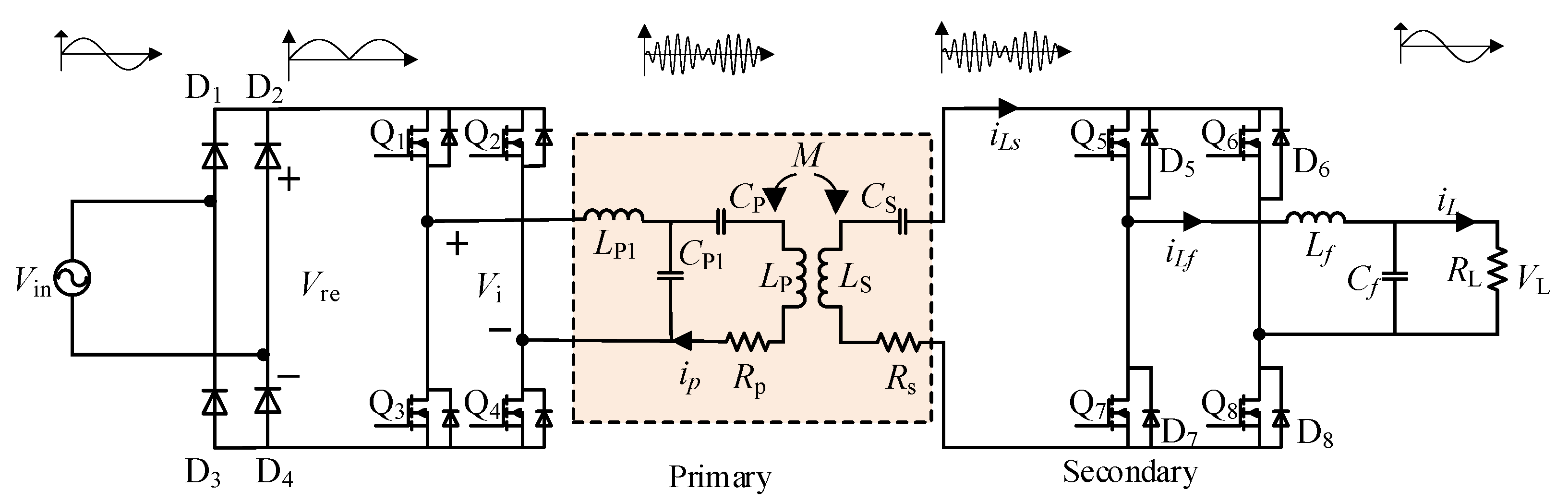
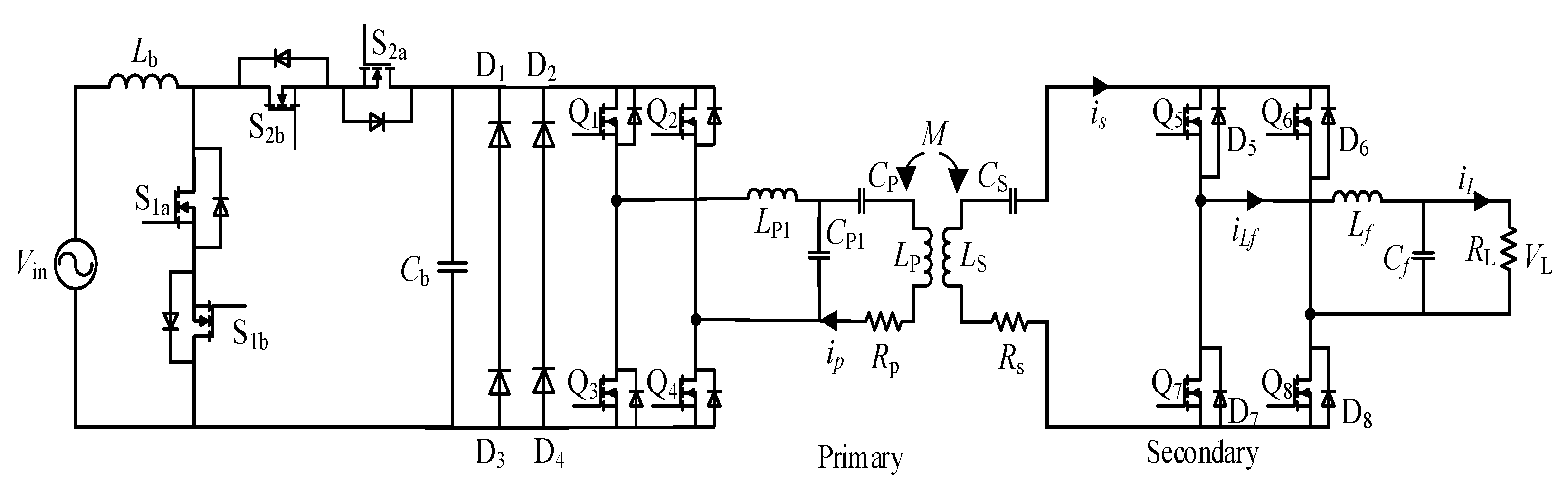
2. Circuit Operation of EM–WPT System

The EM–WPT system can be divided into voltage source system and current source system. The voltage source system usually adopts a series compensation network in the primary side circuit, while the current source system requires a parallel resonant network. This study uses a typical voltage–fed resonant tank as an example. The main LCC–S EM–WPT system is shown in Figure 2.

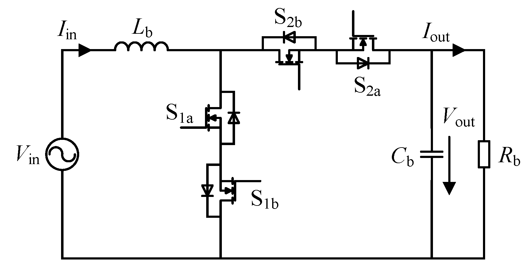
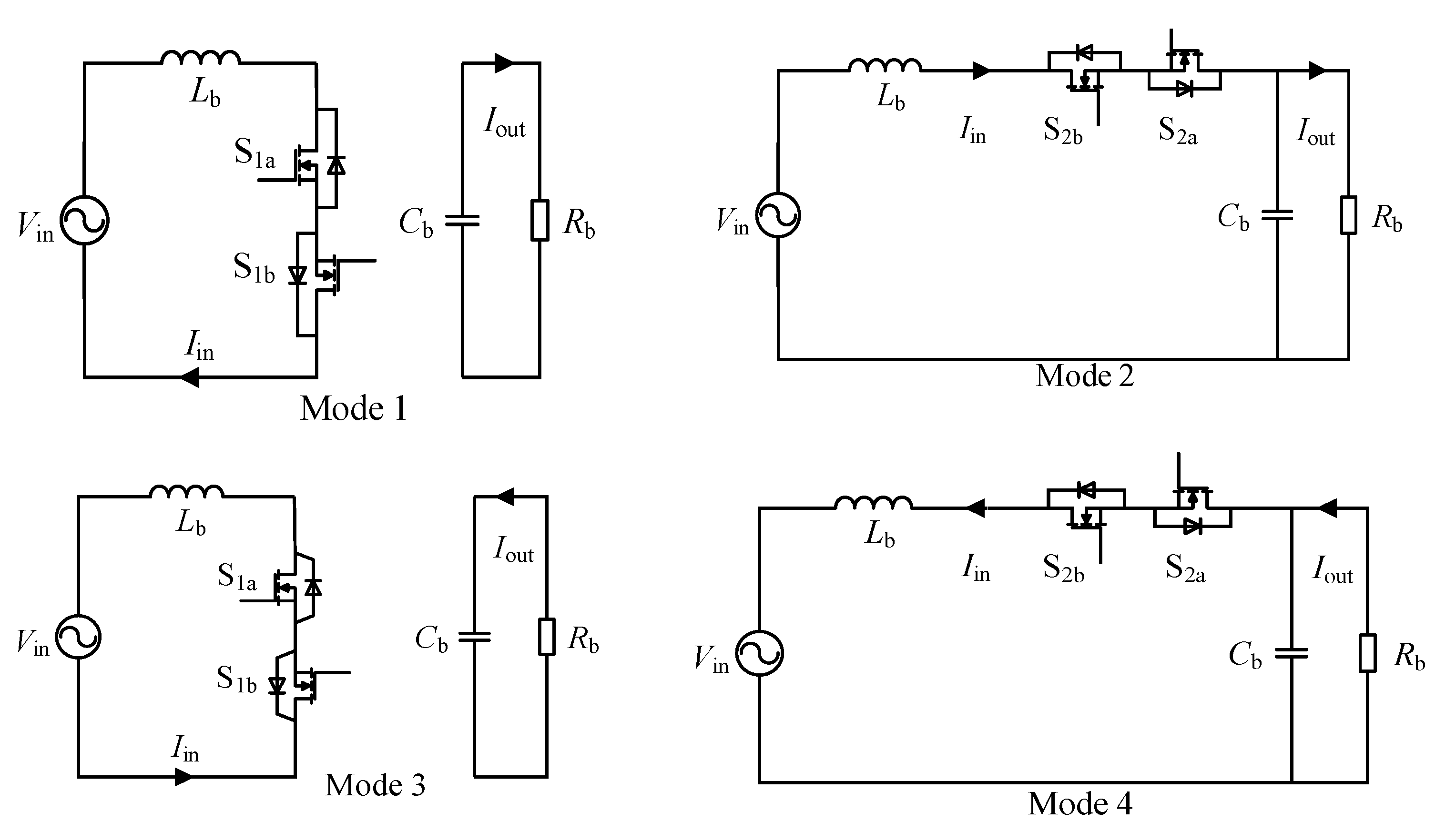
2.1. Primary AC–DC–AC Converter Operation

As shown in Figure 2, Vin is the input AC power. input rectifier bridge is composed of four diodes (D1–D4). The compensation inductor and compensation capacitor for the primary side are LP1 and CP1, respectively. LP and CP are the self-inductances and the series capacitors of the primary side, respectively. Rp is the equivalent series resistance of the primary transmitting coil. Such an LCC resonant network is assumed to be excited by a high frequency inverter to generate a low distortion high frequency sinusoidal current, which creates the zero current switching (ZCS) conditions for the inverter switches (Q1–Q4).
It can also be shown in Figure 2 that the role of the input rectifier bridge (D1–D4) without a large electrolytic capacitor is to perform a full-wave rectification. A series of the high frequency rectangular voltage waveforms, whose amplitude presents an AC envelope change, is converted by the four MOSFETs (Q1–Q4) from the input full-wave power (as shown in Figure 3). Thus, the transmitting coil current is modulated to a barracuda type. The working principle of the primary AC–DC–AC converter is seen in Figure 3.

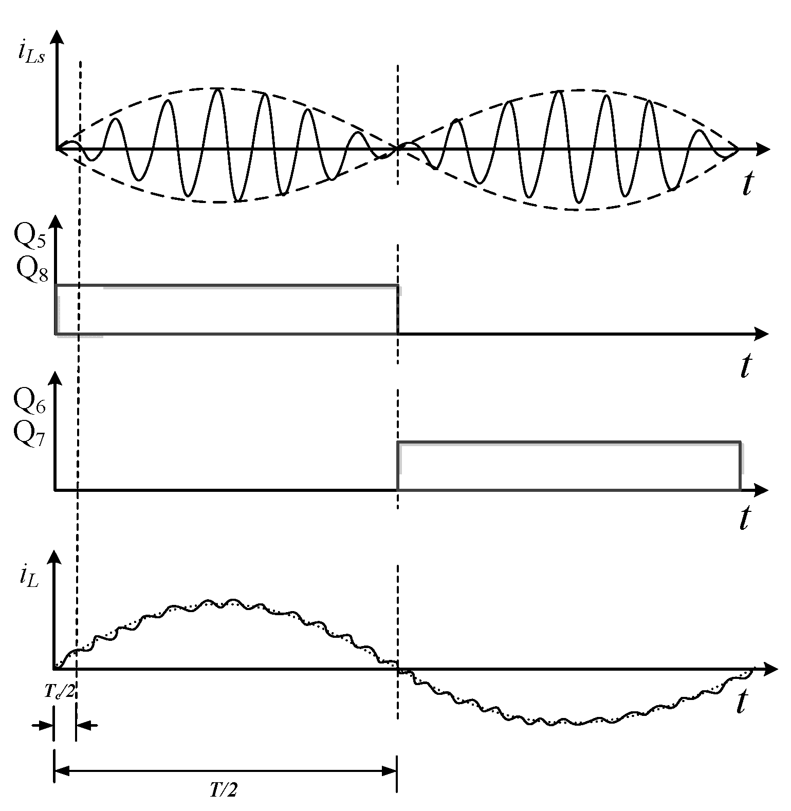
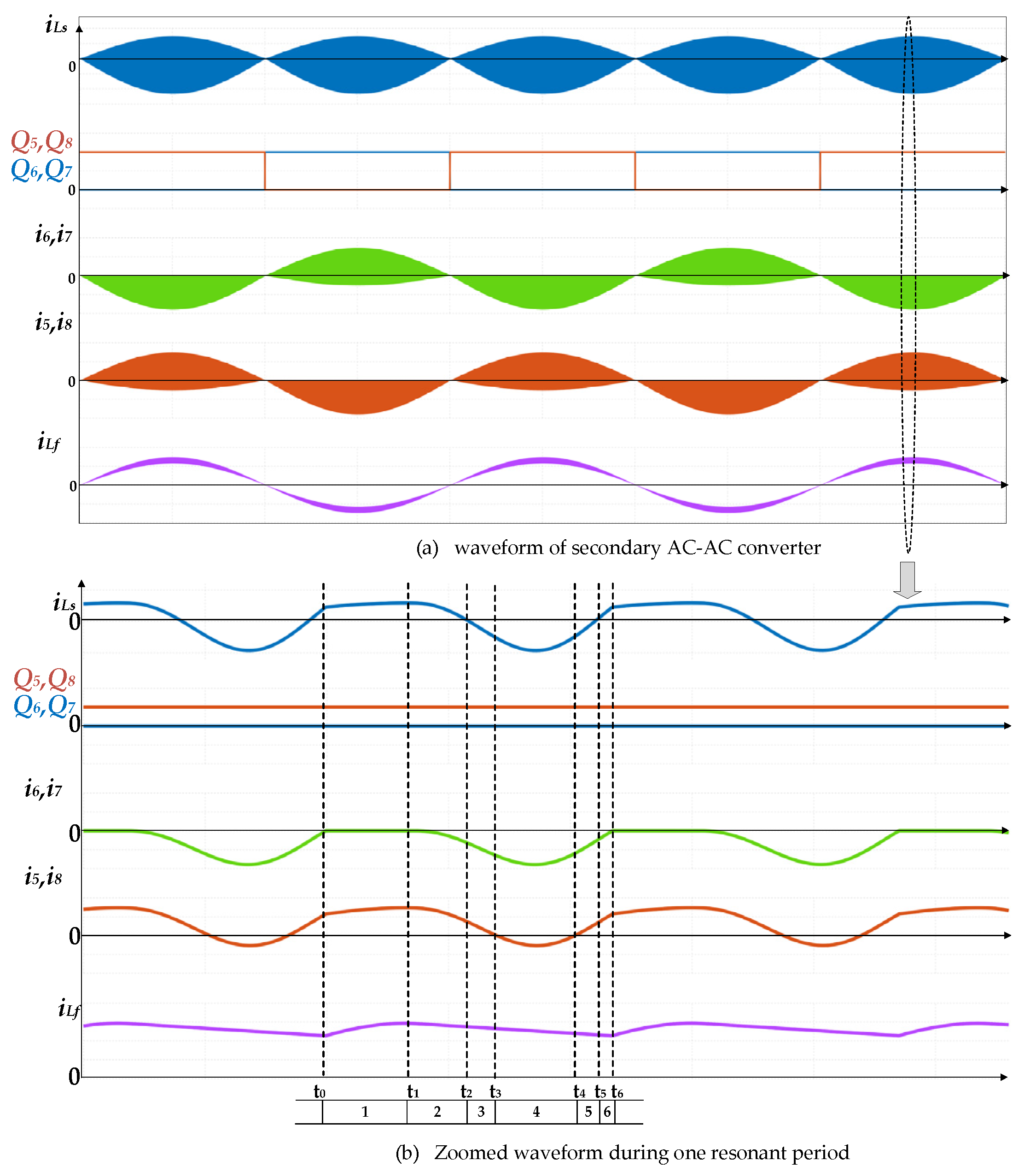
2.2. Secondary AC–AC Converter Operation

The secondary series resonant network consists of Ls and Cs; such a resonant network is completely tuned. M is the mutual inductance of Ls and Lp. The series resonant tank receives the energy by high-frequency magnetic coupling. The equivalent series resistance of the secondary resonant coil is Rs. A low frequency AC output to the load RL is converted directly by the secondary AC–AC converter, which consists of four switches (Q5–Q8) from the induced high frequency AC. The high frequency energy induced in the secondary part also presents a barracuda type, so the role of the side AC–AC converter can be seen as a demodulation of the barracuda–type energy. The working principle of the secondary AC–AC converter is seen in Figure 4.
The secondary side shown in Figure 2 only needs four switches (Q5–Q8) to achieve demodulation, the anti-parallel diodes (D5–D8) of switches of the secondary AC–AC converter are used to provide an energy release circuit for the output filter inductor, and power is provided continuous to the load. During half the cycle of the load voltage, Q5 and Q8 are fully on, and Q6 and Q7 are off (similarly, during the negative half of the load voltage, Q5 and Q8 are always off, and Q6 and Q7 are always on. The structure is symmetrical with the positive half cycle). The waveforms of the secondary AC–AC converter in the positive half cycle of load voltage are shown in Figure 5 and the operation modes of secondary AC-AC converter during one resonant period at iL > 0 are shown in Figure 6.
The secondary side demodulation has six modes in a resonant period, as shown in Figure 6.
Mode–1: Q5 and Q8 are on Q6 and Q7 are off, D1–D8 are off. The output filter circuit and load are connected to the secondary resonant network; the system charges the inductor Lf, and iLf rises.
Mode–2: During Mode 2, the resonant network of the secondary part will start to resonate, and the VLs potential will reverse. It can be observed that D6 and D7 conduct and establish a positive potential. This makes the VLs potential approximate to zero. The inductance Lf releases energy through the diode, and the resonant current iL decreases to zero. The diode currents i6 and i7 increase gradually, and i5 and i8 decrease positively. The inductance current iLf decreases.
Mode–3: The reverse diodes D6 and D7 still have a positive potential. However, due to the voltage clamping after the diode is switched on, the VLs potential is approximately zero. The inductance Lf continues to release energy through the diode-side resonant current iLs increases inversely. The diode currents i6 and i7 continue to increase gradually. The i5 and i8 decrease positively to zero, and the inductance current iLf continues to decrease.
Mode–4: The reverse diodes D6 and D7 still have positive potential. After the diode is switched on, the voltage is clamped, and the VLs potential is approximately zero. The inductance Lf continues to release energy through the diode, and the inductance current iLf continues to decline. The vice-side resonant current iLs reversely resonates. The diode currents i6 and i7 continue to resonate, and i5 and i8 reversely resonate to zero.
Mode–5: The reverse diodes D6 and D7 still have a forward potential, and the VLs potential is approximately zero. The inductor Lf continues to release energy through the diode, and the inductor current iLf continues to decrease. The secondary resonant current iLs reverses to zero, and the diode current i6 and i7 continue to gradually decrease in the same direction; i5 and i8 increase in the positive direction.
Mode–6: The reverse diodes D6 and D7 still have a positive potential, and the potential of VLs is approximately zero. The inductance Lf continues to release energy through the diode, and the inductance current iLf continues to decrease. The secondary resonant current iLs increases positively, and i5 and i8 increase positively. The directions of the diode current i6 and i7 remain unchanged, and gradually decrease to a zero cutoff, followed by the first mode.

3. Topological Characteristics Analysis and Control Strategy of CC and CV Output

3.1. LCC–S Topological Characteristics Analysis

Based on the AC impedance analysis method, the impedance and frequency characteristics of the WPT system can be explored, and the system can be analyzed from the perspective of the frequency domain. Assuming that all of the switching devices are ideal switches and the filter circuit is an ideal filter, and the energy enters the load without a loss as shown in Figure 7, the impedance model of the LCC–S EM–WPT system can be easily obtained.
As is shown in Figure 7, Vi is the excitation voltage of the primary resonance compensation tank; Ip, Is is the current of the transmitter coil and the receiver coil, respectively; Iin is the network input current, ICP1 is the current of the compensation capacitor CP1; ω is the system operating angular frequency. According to Figure 7, the KVL equations of the primary and secondary circuits of the LCC–S WPT system can be obtained as
{ j ω L P 1 I i n + I C P 1 j ω C P 1 = V i ( j ω L P + 1 j ω C P + R P ) I P I C P 1 j ω C P 1 j ω M I S = 0 ( j ω L S + 1 j ω C S + R S + R L ) I S j ω M I P = 0 I i n = I C P 1 + I P
The input impedance Zin of primary side and input impedance ZS of the secondary side are respectively given in the following Equation:
{ Z in = j ω L P 1 + 1 j ω C P 1 + 1 j ω L P + 1 j ω C P + R P + Z R Z S = j ω L S + 1 j ω C S + R S + R L
ZR is the reflection impedance from the secondary side to the primary side, and its expression is
Z R = ω 2 M 2 j ω L S + 1 j ω C S + R S + R L
In order to enhance the power transmission capability of the EM–WPT system, reactive power compensation is needed to perform on the system to make the system work in resonance. The system working angular frequency is ω = ω0 and ω0 is the resonance angular frequency of system. Under the condition of complete resonance of the system, the inductance and capacitance no longer consume energy, and the primary and secondary circuit impedances of the system are pure resistance. Thus, the values of the compensation components required to achieve resonance at the angular resonance frequency ω0 need to satisfy the following expression:
ω 0 = 1 L P 1 C P 1 = 1 L S C S = 1 L P C P 1 + 1 L P C P
When the system resonance network parameters meet Equation (4), the input impedance Zin, the current in the primary coil Ip and the pickup coil Ip can be obtained as
{ Z in = L P 1 2 M 2 R L I P = V i j ω L P 1 I S = M V i L P 1 ( R S + R L )
Finally, the resistance load RL voltage of the LCC–S WPT system and also the system output voltage, can be written as
V L = I S R L = M R L V i L P 1 ( R S + R L )
The simplification can be done when RL is much higher than RS, so the system output voltage and output current can be derived respectively as
V L M V i L P 1
I L = I S M V i R L L P 1
It can be seen from Equations (7) and (8) that under the resonance state, the output voltage of the LCC–S EM–WPT system is independent of the load, and is only affected by the input voltage Vi, the inductance LP1 and the mutual inductance M. The load current IL is affected by both load RL and input Vi.

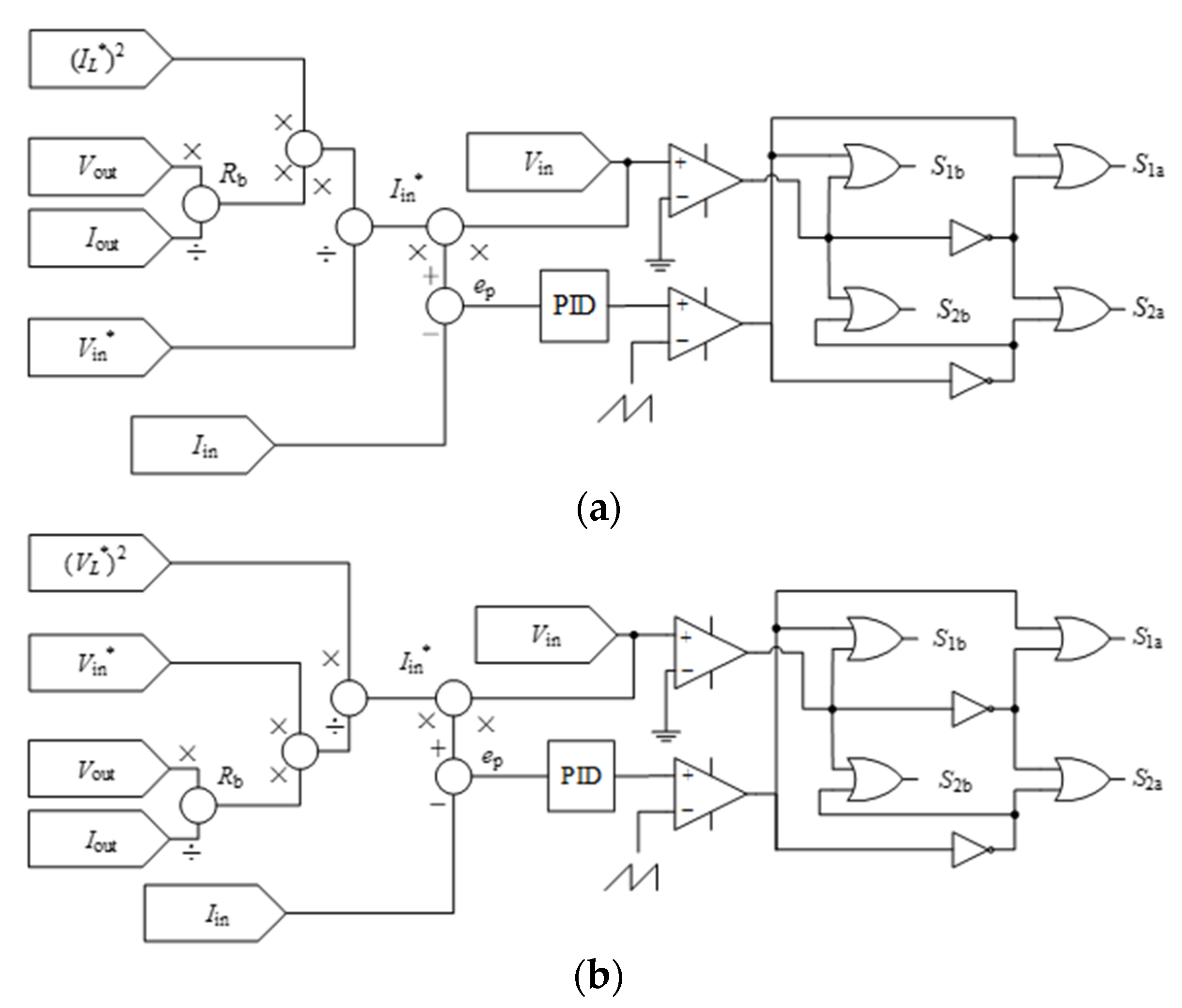
3.2. Control Strategy of CC and CV Output

According to Equation (7), when the system resistance load RL is much larger than the system internal resistance, the output voltage expression of the LCC–S WPT system is
V L = M V i L P 1 = j ω 0 M I P
The primary side current Ip can remain constant as long as the input voltage Vi remains unchanged. Therefore, the load voltage VL of the LCC–S EM–WPT system can remain constant when the load changes. However, if the input grid voltage fluctuates, the constant current condition of the primary coil becomes invalid. In order to achieve constant current on the primary side, it is necessary to add an AC–AC boost converter in front of the full–wave rectifier circuit, which is shown in Figure 8. The primary coil current IP can be kept constant by adjusting the input current of the converter when the grid voltage fluctuates or the load fluctuates. Finally, the AC CV output is achieved.
Based on the principle of energy conservation, the input and output power can be given as
I L 2 R L = V in I in
According to Equation (6), and taking into account the equivalent characteristics of the rectifier bridge load, it can be obtained that the load at full resonance of the system is
R L = π 2 M 2 V o u t 8 L P 1 2 I o u t
The boost circuit used in the DC–DC converter has a continuous input current, the input and output have the same polarity, and the structure is simple and easy to control. However, in AC–AC conversion applications, it is necessary to add a reverse switch tube to cope with the negative half–cycle of the alternating current, so as to realize the AC–AC conversion. The circuit is shown in Figure 9 [33].
In order to analyze the AC–AC boost converter, the circuit after the rectifier bridge is equivalent as Rb and the circuit can be shown as Figure 9. In Figure 9, Lb is the energy storage inductor; Cb is the energy storage capacitor; Rb is the equivalent load of the converter’s subsequent circuit; Iin is the input current, that is, the current flowing through the inductor Lb; Iout is the output current; and S1a, S2a, S1b and S2b are power switch tubes.
According to the change of input voltage polarity and the inductance current, the AC–AC Boost converter has four operating modes as shown in Figure 10:
Mode1 (Vin > 0, Iin increase): S1b and S2b are always turned on, S1a is turned on, S2a is turned off, and the inductor current Iin flows through the inductor Lb, the switching tubes S1a and S1b, and then returns to the power supply. During this time, the inductor Lb is in an energy storage state, and the inductor current Iin increases; the capacitor Cb discharges the load Rb, and the output current Iout decreases.
Mode2 (Vin > 0, Iin decrease): S1b and S2b are always on, S2a is on, and S1a is off. The inductor current Iin flows through the inductor Lb, the switches S2a and S2b, and then flows through the capacitor Cb and the resistive load Rb to return to the power supply. During this time, the inductor Lb is in a discharged state, and the inductor current Iin decreases; the output current Iout increases.
Mode3 (Vin < 0, Iin increase): S1a and S2a are always turned on, S1b is turned on, and S2b is turned off. The inductor current Iin returns to the power supply after passing through the inductor Lb, the switching tubes S1a and S1b, as shown in Figure 8. At this time, the inductor Lb is in an energy storage state, and the inductor current Iin increases; the capacitor Cb discharges the load, and the output current Iout decreases.
Mode4 (Vin > 0, Iin decrease): S1a and S2a are always on, S2b is on, and S1b is off. The inductor current Iin flows through the inductor Lb, the switches S2a and S2b, and then flows through the capacitor Cb and the resistive load Rb to return to the power supply, as shown in Figure 9. At this time, the inductor Lb is in a discharged state, and the inductor current Iin decreases; the output current Iout increases.
Through the analysis of the four operation modes of the AC–AC boost converter, it can be known that if the output current Iout is to be controlled to be constant, it can be achieved by controlling the change of the inductor current Iin. Assuming that the AC–AC boost converter has no energy loss, according to the conservation of Energy, by substituting Equation (11) into Equation (10), the input current reference Iin* with CC mode can be found as
I in * = I L 2 R L V in = π 2 M 2 I L 2 V o u t 8 L P 1 2 V in I o u t ( C C m o d e )  
the input current reference Iin* with CV mode can be obtained as
I in * = V L 2 R L V in = 8 L P 1 2 I o u t V L 2 π 2 M 2 V o u t V in ( C V m o d e )  
In Equation (8), if the system coupling device and the compensation network parameters remain unchanged, the mutual inductance M and Lp1 remain unchanged, assuming the input voltage remains unchanged, then the constant control of the output current can be achieved through detecting the output voltage Vout and the output current Iout; on the contrary, if the load does not change, the input voltage sags, then the input voltage needs to be detected to achieve a CC control. Therefore, the control logic of the AC–AC Boost converter with CC and CV output of the LCC–S EM–WPT system is shown in Figure 11 and the overall circuit structure of the system is shown in Figure 12.

4. Experiment Verification

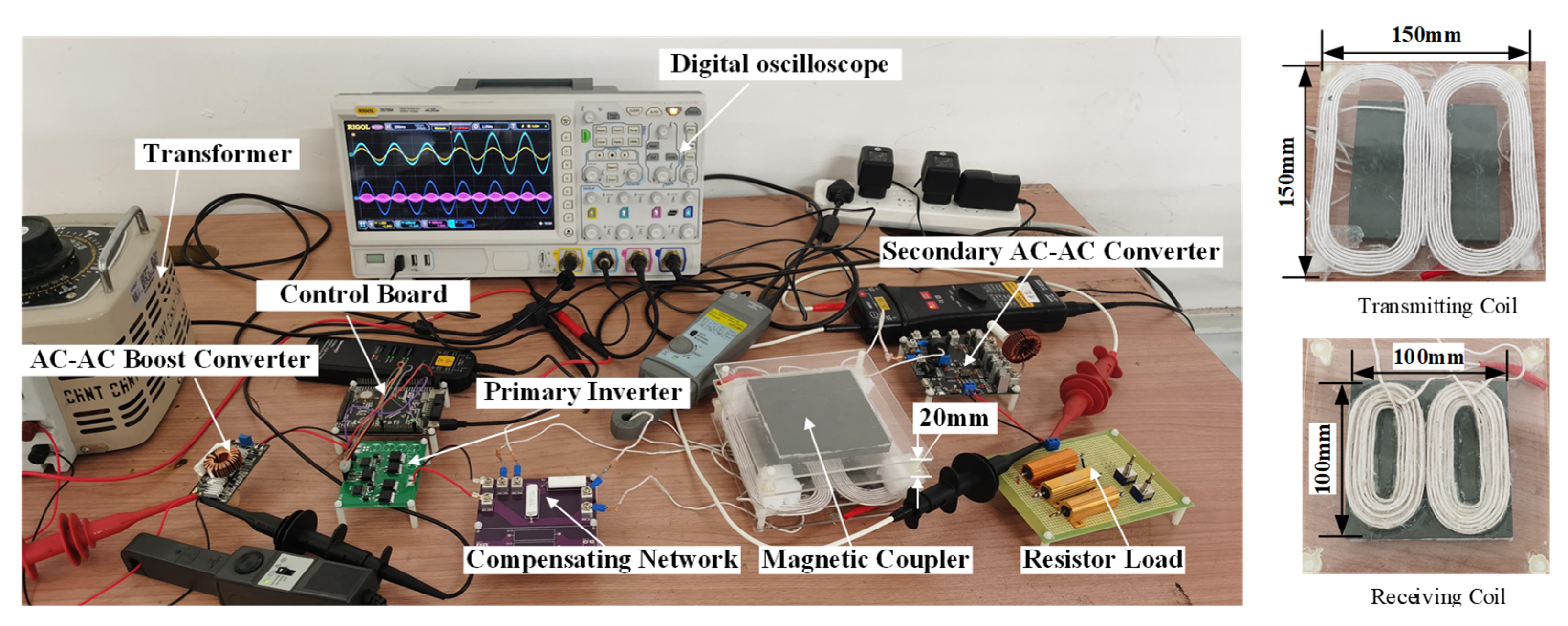
4.1. Setup of Experiment

In order to verify the CC and CV characteristics of the LCC–S EM–WPT system, an experimental prototype is fabricated, as is shown in Figure 13. The parameters are consistent with those in Table 1. According to SAE j2954 [34], the operating frequency of the system is set at 85kHz. Thus, SiC MOSFETs (IPP057N08N3G,80V/80A) are used in the primary and secondary converters and are driven by the high– and low–side gate driver IC (2EDS9265H). The Hall current sensor (ACS712–20A) is used to sample the current, the controller is STM32F407ZG. The size of the transmitting coil is 150 mm × 150 mm and the size of the receiving coil is 100 mm × 100 mm. The distance between transmitting and receiving coils is 20 mm. All the coils in the resonant network are made by the Litz wire with 200 strands. The coils are designed into a DD structure to eliminate the cross coupling effect caused by the transmitting coil.

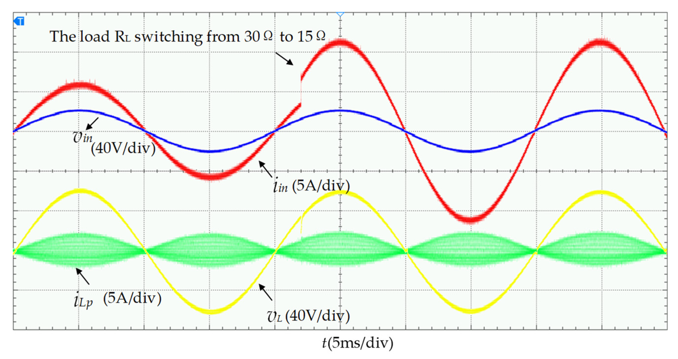
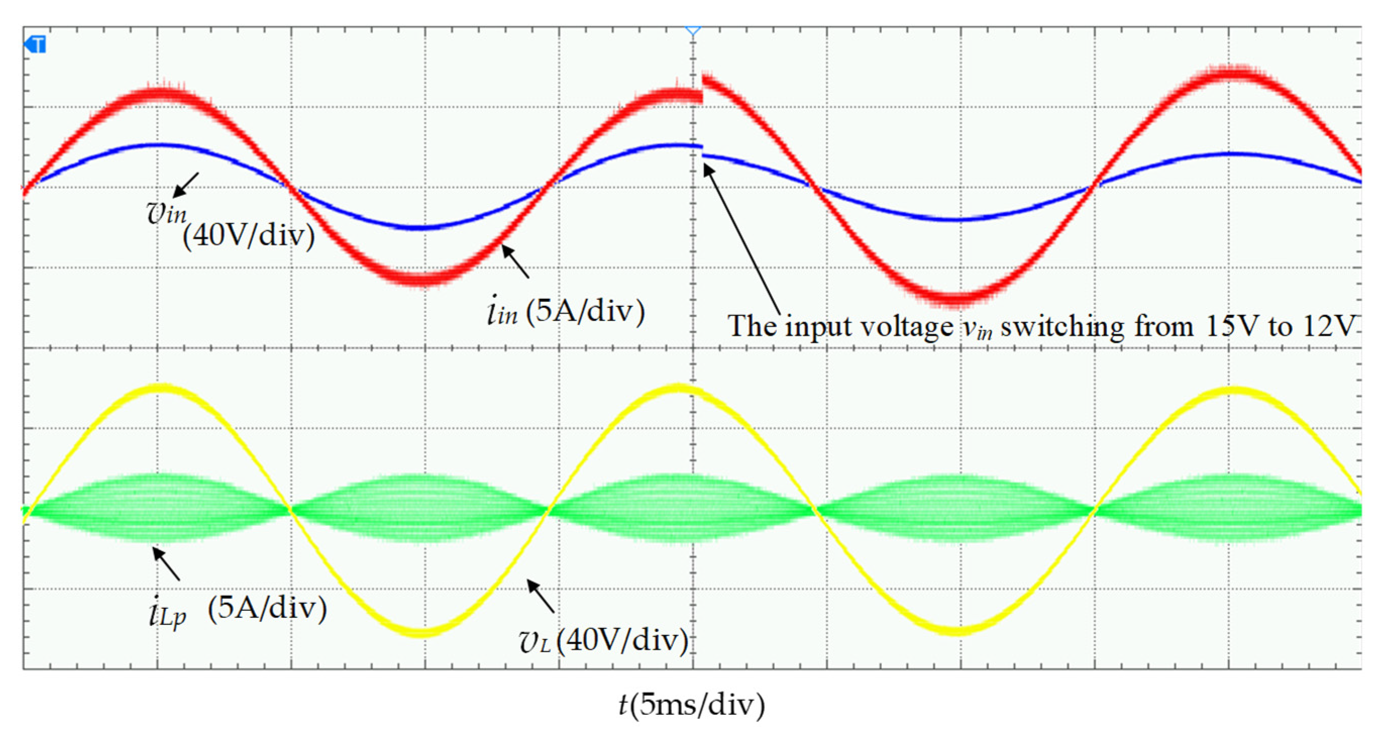
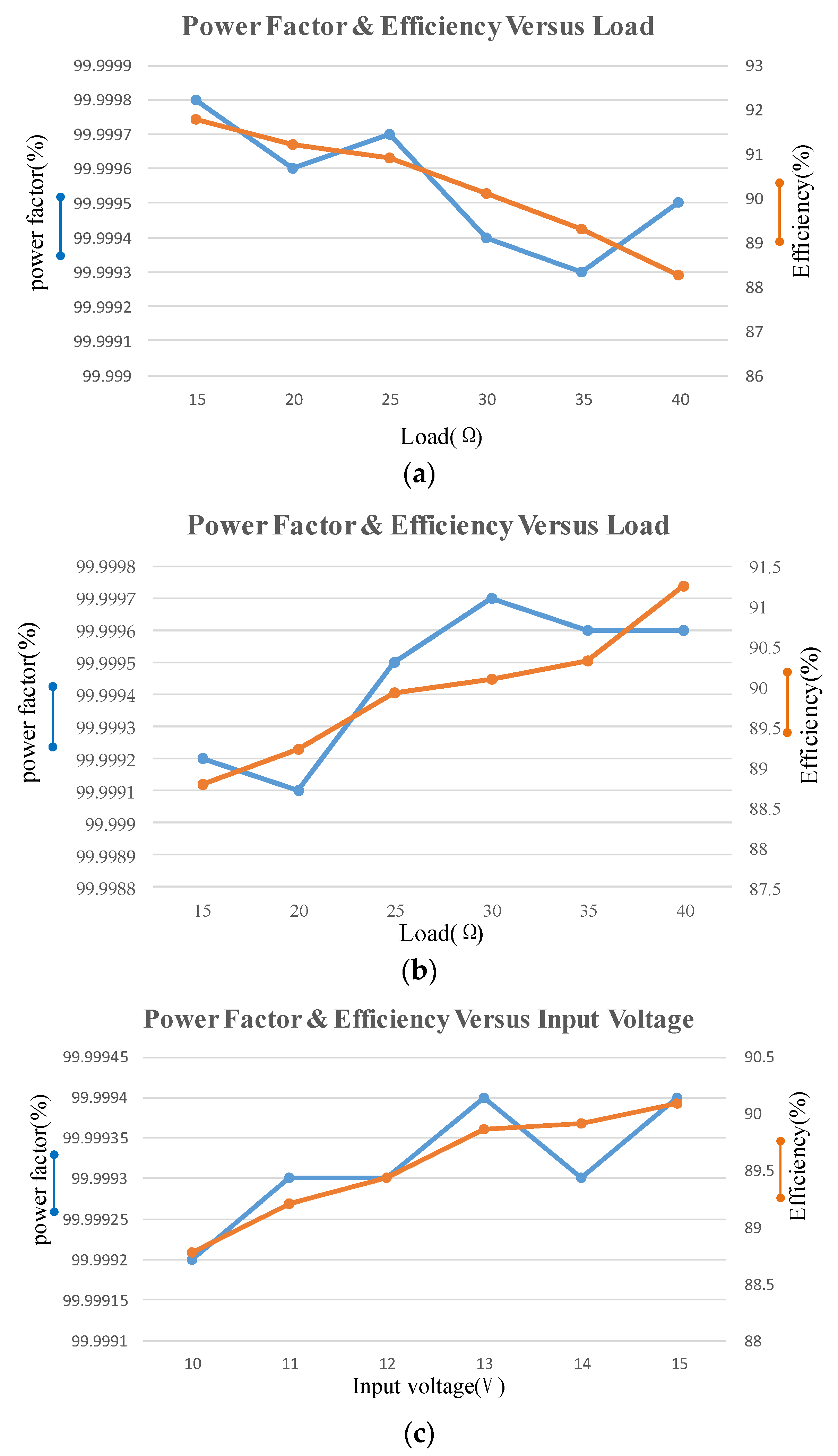
4.2. Analysis of Experimental Results

As per the parameters in Table 1. The experimental results of the proposed WPT system are shown below.
Figure 14 shows that when the load RL step from 30–50 Ω, the peak value of resonant current iin increases from 9A to 15A, the amplitude of output load current iL remains at 1.98 A, and the frequency remains at 49.7 Hz. The primary current iLp presents an envelope modulation shape and its value increases as the load switches. The experimental results are lower than the theoretical values obtained under ideal conditions. This is due to the coil resistance loss and the conduction loss of the converter in the actual system. In addition, the input current iL shown in Figure 13 increases slightly, which is due to the decrease of the reflection impedance and the increase in the input current after load switching. The load current ripple is mainly caused by the discharge time of the output filter capacitor Cf affected by the load resistance mutation. Considering that the system power is reduced by 40% under dynamic load switching, such a slight current ripple is not enough to affect our conclusion that the system has CC characteristics.
Figure 15 shows that peak resonant current iin rises to 11 A from 5.5 A when the load RL steps up from 30 Ω to 15 Ω, while the peak value of the load voltage VL still maintains at 49.6 V and the output AC frequency remains at 49.8 Hz. The primary current iLp remains constant during the load switching. Similarly, compared with the theoretical values obtained under ideal conditions, the experimental results are lower. The power of the system is doubled under the dynamic load switching condition; moreover, the load voltage VL shown in Figure 15. has no obvious overshoot during the load switching. This proves that the system does have the CC characteristic.
Figure 16 shows that the peak resonant current iin rises to 7 A from 5.5 A as the input grid voltage sags from 15 V to 12 V, while the peak value of the output load voltage VL still maintains at 49 and the output AC frequency remains at 49.7 Hz. The primary current iLp remains constant after the input grid voltage sag. The load voltage VL shown in Figure 16 also has no obvious overshoot when the input grid voltage sag happens. Actually, the fact that the power of the system is unchanged under the condition of an input grid voltage sag proves that the AC–AC boost converter is automatically adjusting the input power to maintain a constant output voltage.
From Figure 14, Figure 15 and Figure 16, the input current is very sinusoidal. The measured input power factor and efficiency are all plotted in Figure 17. From the perspective of an input power factor, under the conditions of the whole load range and input voltage fluctuation, the overall input power factor of the envelope modulation WPT system is close to 1. It is verified that the system not only has a high power factor, but can also better suppress the pollution of the high–frequency harmonic current reflected by the EM–WPT system on the power side. Under the CC characteristic, with the increase of the load resistance, the output power increases as the input current of the AC–AC boost converter begins to rise, and as the heat loss begins to increase, the system efficiency will decrease, which is a normal phenomenon. Similarly, under CV characteristics, with the increase in the load resistance, the output power decreases, the input current of boost converter begins to decrease, the heat loss decreases, and the system efficiency will increase. In short, the maximum measured efficiency was 91.78% and the measured input power factor approached unity.

5. Conclusions

This paper presents an EM–WPT system combined with an AC–AC boost converter for AC load applications. The AC–DC–AC converter on the system’s primary side is used to realize the high frequency envelope modulation of low frequency AC power, and the secondary direct AC–AC converter is to demodulate the envelope energy and output AC power to the load. Based on the conservation of energy, controlling the inductor current of the power supply in the closed–loop design not only realizes the CC and CV output of the load, but also achieves a high–quality source current. Both the working principle of the system’s converters and the LCC–S compensation topology are analyzed and designed in detail in this paper. Furthermore, experiments have been carried out and verified which show that the system has a high power factor and transmission efficiency, and can realize an AC constant voltage and constant current output despite the load change and input power sag. However, the magnetic coupling mechanism suitable for the EM–WPT system is not the focus of the paper and is yet to be studied.

Author Contributions

Conceptualization, L.Z. and Y.Y.; Methodology, L.Z.; Software, H.L.; Validation, Q.G. and S.X.; Formal analysis, L.Z.; Writing—Original Draft Preparation, L.Z.; Writing—Review and Editing, L.Z. and Y.Y.; Funding acquisition, L.Z. and Y.Y. All authors have read and agreed to the published version of the manuscript.

Funding

This research was financially supported by the Science and Technology Research Program of Chongqing Municipal Education Commission (KJQN201801142&KJQN202001144).

Conflicts of Interest

The authors declare no conflict of interest.

References

  1. Harshitha, H.M.; Sureshkumar, S.; Stacey, S.A.; Zabiulla, S.I.; Kumar, R.R. Wireless Power Transfer to Charge Low Power Device. In Proceedings of the 2021 International Conference on Design Innovations for 3Cs Compute Communicate Control, Bangalore, India, 10–11 June 2021; pp. 61–64. [Google Scholar]
  2. Lee, H.; Jung, S.; Huh, Y.; Kim, S.J. Wireless Power Receiver with Wide Dynamic Range for Biomedical Implants. In Proceedings of the 2019 IEEE Wireless Power Transfer Conference, London, UK, 18–21 June 2019; pp. 241–244. [Google Scholar]
  3. Yan, Z.; Song, B.; Zhang, Y.; Zhang, K.; Mao, Z.; Hu, Y. A Rotation-Free Wireless Power Transfer System with Stable Output Power and Efficiency for Autonomous Underwater Vehicles. IEEE Trans. Power Electron. 2019, 34, 4005–4008. [Google Scholar] [CrossRef]
  4. Chen, L.J.; Boys, J.T.; Covic, G.A. Power Management for Multiple-Pickup IPT Systems in Materials Handling Applications. IEEE J. Emerg. Sel. Top. Power Electron. 2015, 3, 163–176. [Google Scholar] [CrossRef]
  5. Zhang, Y.; Chen, S.; Li, X.; Tang, Y. Design Methodology of Free-Positioning Nonoverlapping Wireless Charging for Consumer Electronics Based on Antiparallel Windings. IEEE Trans. Ind. Electron. 2022, 69, 825–834. [Google Scholar] [CrossRef]
  6. Pries, J.; Galigekere, V.P.N.; Onar, O.C.; Su, G. A 50-kW Three-Phase Wireless Power Transfer System Using Bipolar Windings and Series Resonant Networks for Rotating Magnetic Fields. IEEE Trans. Power Electron. 2020, 35, 4500–4517. [Google Scholar] [CrossRef]
  7. Wu, L.; Zhang, B.; Zhou, J. Efficiency Improvement of the Parity-Time-Symmetric Wireless Power Transfer System for Electric Vehicle Charging. IEEE Trans. Power Electron. 2020, 35, 12497–12508. [Google Scholar] [CrossRef]
  8. Machura, P.; Santis, V.D.; Li, Q. Driving Range of Electric Vehicles Charged by Wireless Power Transfer. IEEE Trans. Veh. Technol. 2020, 69, 5968–5982. [Google Scholar] [CrossRef]
  9. Chu, S.Y.; Cui, X.; Zan, X.; Avestruz, A.T. Transfer-Power Measurement Using a Non-Contact Method for Fair and Accurate Metering of Wireless Power Transfer in Electric Vehicles. IEEE Trans. Power Electron. 2022, 37, 1244–1271. [Google Scholar] [CrossRef]
  10. Samanta, S.; Rathore, A.K. A New Inductive Power Transfer Topology Using Direct AC–AC Converter with Active Source Current Waveshaping. IEEE Trans. Power Electron. 2018, 33, 5565–5577. [Google Scholar] [CrossRef]
  11. Huynh, P.S.; Vincent, D.; Azeez, N.A.; Patnaik, L.; Williamson, S.S. Performance Analysis of a Single-Stage High-Frequency AC-AC Buck Converter for a Series-Series Compensated Inductive Power Transfer System. In Proceedings of the 2018 IEEE Transportation Electrification Conference and Expo, Long Beach, CA, USA, 13–15 June 2018; pp. 347–352. [Google Scholar]
  12. Weerasinghe, S.; Madawala, U.K.; Thrimawithana, D.J. A Matrix Converter-Based Bidirectional Contactless Grid Interface. IEEE Trans. Power Electron. 2017, 32, 1755–1766. [Google Scholar] [CrossRef]
  13. Wang, Z.H.; Sun, Y.; Dai, X.; Tang, C.S. Design of converter of DC-AC type contactless power transfer system. J. Chongqing Univ. 2011, 34, 38–43. [Google Scholar]
  14. Wang, Z.H.; Sun, Y.; Su, Y.G.; Dai, X.; Tang, C.S. A new type AC/DC/AC converter for contactless power transfer system. Trans. China Electrotech. Soc. 2010, 25, 84–89. [Google Scholar]
  15. Safaee, A.; Yazdani, D.; Bakhshai, A.; Jain, P.K. Multiblock Soft-Switched Bidirectional AC–AC Converter Using a Single Loss-Less Active Snubber Block. IEEE Trans. Power Electron. 2012, 27, 2260–2272. [Google Scholar] [CrossRef]
  16. Wu, H.H.; Covic, G.A.; Boys, J.T.; Robertson, D.J. A Series-Tuned Inductive-Power-Transfer Pickup with a Controllable AC-Voltage Output. IEEE Trans. Power Electron. 2011, 26, 98–109. [Google Scholar] [CrossRef]
  17. Li, H.L.; Hu, A.P.; Covic, G.A. A Direct AC–AC Converter for Inductive Power-Transfer Systems. IEEE Trans. Power Electron. 2012, 27, 661–668. [Google Scholar] [CrossRef]
  18. Wu, H.H.; Covic, G.; Boys, J. A low energy storage IPT system using AC processing controllers. In Proceedings of the 2011 6th IEEE Conference on Industrial Electronics and Applications, Beijing, China, 21–23 June 2011; pp. 351–356. [Google Scholar]
  19. Natanzi, A.J.; Vaez-Zadeh, S.; Babaki, A.; Zakerian, A. A Single-Phase Wireless Power Transfer System with a High-Frequency AC Link Converter in the Secondary for Three-Phase Applications. In Proceedings of the 2021 12th Power Electronics, Drive Systems, and Technologies Conference, Tabriz, Iran, 2–4 February 2021; pp. 1–5. [Google Scholar]
  20. Babaki, A.; Vaez-Zadeh, S.; Zakerian, A.; Natanzi, A.J. Analysis and Control of Wireless Motor Drives with a Single Inverter in Primary Side. IEEE Trans. Energy Convers. 2021, 36, 930–939. [Google Scholar] [CrossRef]
  21. Babaki, A.; Vaez-Zadeh, S.; Jahanpour-Dehkordi, M.; Zakerian, A. Wireless Motor Drives with a Single Inverter in Primary Side of Power Transfer Systems. In Proceedings of the 2019 IEEE PELS Workshop on Emerging Technologies: Wireless Power Transfer, London, UK, 18–21 June 2019; pp. 125–128. [Google Scholar]
  22. Bac, N.X.; Vilathgamuwa, D.M.; Madawala, U.K. A SiC-Based Matrix Converter Topology for Inductive Power Transfer System. IEEE Trans. Power Electron. 2014, 29, 4029–4038. [Google Scholar]
  23. Ota, H.; Liu, J.; Miura, Y.; Yanagisawa, Y.; Wada, A.; Sakabe, S.; Bevrani, H.; Ise, T. Multiphase Direct AC Wireless Power Transfer System: Comparative Proposals Using Frequency and Amplitude Modulations. IEEE J. Emerg. Sel. Top. Ind. Electron. 2021, 2, 101–112. [Google Scholar] [CrossRef]
  24. Jiang, C.; Chau, K.T.; Wang, H.; Lee, C.H.T.; Ching, T.W. Wireless Secondary-Converterless Bipolar Drive for AC Application. In Proceedings of the IECON 2019—45th Annual Conference of the IEEE Industrial Electronics Society, Lisbon, Portugal, 14–17 October 2019; pp. 4475–4480. [Google Scholar]
  25. Yan, Z.; Zhang, Y.; Song, B.; Zhang, K.; Kan, T.; Mi, C. An LCC-P Compensated Wireless Power Transfer System with a Constant Current Output and Reduced Receiver Size. Energies 2019, 12, 172. [Google Scholar] [CrossRef] [Green Version]
  26. Mahesh, A.; Chokkalingam, B.; Mihet-Popa, L. Inductive Wireless Power Transfer Charging for Electric Vehicles—A Review. IEEE Access 2021, 9, 137667–137713. [Google Scholar] [CrossRef]
  27. ElGhanam, E.; Hassan, M.; Osman, A. Design of a High Power, LCC-Compensated, Dynamic, Wireless Electric Vehicle Charging System with Improved Misalignment Tolerance. Energies 2021, 14, 885. [Google Scholar] [CrossRef]
  28. Lu, S.; Deng, X.; Shu, W.; Wei, X.; Li, S. A New ZVS Tuning Method for Double-Sided LCC Compensated Wireless Power Transfer System. Energies 2018, 11, 307. [Google Scholar] [CrossRef] [Green Version]
  29. Zhang, X.; Lai, Z.; Xiong, R.; Li, Z.; Zhang, Z.; Song, L. Switching Device Dead Time Optimization of Resonant Double-Sided LCC Wireless Charging System for Electric Vehicles. Energies 2017, 10, 1772. [Google Scholar] [CrossRef] [Green Version]
  30. Ali, N.; Liu, Z.; Armghan, H.; Ahmad, I.; Hou, Y. LCC-S-Based Integral Terminal Sliding Mode Controller for a Hybrid Energy Storage System Using a Wireless Power System. Energies 2021, 14, 1693. [Google Scholar] [CrossRef]
  31. Ali, N.; Liu, Z.; Hou, Y.; Armghan, H.; Wei, X.; Armghan, A. LCC-S Based Discrete Fast Terminal Sliding Mode Controller for Efficient Charging through Wireless Power Transfer. Energies 2020, 13, 1370. [Google Scholar] [CrossRef] [Green Version]
  32. Zhang, L. Research on Key Issues of Envelope Modulation Wireless Power Transfer Systems. Ph.D. Thesis, Chongqing University, Chongqing, China, 2017. [Google Scholar]
  33. Kabir, M.A.; Abedin, A.H.; Mustafiz, R.B.; Islam, M.K.; Choudhury, M.A. A Single Phase AC-AC Boost Converter with Improved Input Power Factor and THD. In Proceedings of the International Aegean Conference on Electrical Machines and Power Electronics and Electromotion, Joint Conference, Istanbul, Turkey, 8–10 September 2011; pp. 764–767. [Google Scholar]
  34. SAE International. Wireless Power Transfer for Light-Duty Plug-in/Electric Vehicles and Alignment Methodology. SAE J2954; SAE International: Warrendale, PA, USA, 2019. [Google Scholar]
Figure 1. Typical WPT system for EV charging applications.
Energies 15 01562 g001
Figure 2. Typical LCC–S EM–WPT system.
Energies 15 01562 g002
Figure 3. Working principle of the primary AC–DC–AC converter.
Energies 15 01562 g003
Figure 4. Working principle of the secondary AC–AC converter.
Energies 15 01562 g004
Figure 5. Waveforms of the secondary AC–AC converter in the positive half cycle of the load voltage.
Energies 15 01562 g005
Figure 6. Operation modes of AC–AC converter in one resonance cycle at iL> 0. (a) mode–1; (b) mode–2; (c) mode–3; (d) mode–4; (e) mode–5. (f) mode–6.
Energies 15 01562 g006
Figure 7. LCC–S WPT system impedance model.
Energies 15 01562 g007
Figure 8. Primary boost AC–DC–AC converter.
Energies 15 01562 g008
Figure 9. AC–AC boost converter.
Energies 15 01562 g009
Figure 10. Mode of the AC–AC boost converter.
Energies 15 01562 g010
Figure 11. Control block diagram of CC and CV output of AC–AC boost converter. (a) Control block diagram of CC output. (b) Control block diagram of CV output.
Energies 15 01562 g011
Figure 12. Circuit diagram of the proposed LCC–S EM–WPT system.
Energies 15 01562 g012
Figure 13. Experimental prototype.
Energies 15 01562 g013
Figure 14. Experimental results of proposed EM–WPT system with the load RL1 switching from 30–50 Ω of CC mode.
Energies 15 01562 g014
Figure 15. Experimental results of proposed EM–WPT system with the load RL1 switching from 30–15 Ω of CV mode.
Energies 15 01562 g015
Figure 16. Experimental results of proposed EM–WPT system with the input voltage vin switching from 15 V to 12 V of CV mode.
Energies 15 01562 g016
Figure 17. Measured input power factor and efficiency with CC mode and CV mode. (a) Power factor and efficiency versus load with CC mode. (b) Power factor and efficiency versus load with CV mode. (c) Power factor and efficiency versus input voltage with CV mode.
Energies 15 01562 g017
Table 1. System Parameters.
ParametersSymbolValue
Input AC supply magnitude (V)Vin15
Supply frequency (Hz)fin50
Boost energy storage inductance (μH)Lb20
Boost capacitance filter (μF)Cb2
Secondary inductance filter (μH) Lf1000
Secondary capacitance filter (μF)Cf0.274
Nominal resonant frequency (kHz)f085
Resonant inductance of primary side (μH)Lp217.1
Resonant capacitance of primary side (μF)Cp0.019
compensation inductorLp133.737
compensation capacitorCp10.104
Resonant inductance of secondary side (μH)Ls217.69
Resistance of secondary resonant inductor (Ω)Cs0.016
Mutual inductance (μH)M101.21
Resistance of primary resonant inductor (Ω)Rp0.074
Resistance of secondary resonant inductor (Ω)Rs0.077
Resistance of the load (Ω)RL30
AC output load voltage (V)VL50
AC output load current (A)IL2
Publisher’s Note: MDPI stays neutral with regard to jurisdictional claims in published maps and institutional affiliations.

