1. Introduction
The current source converter offers an alternative solution to the voltage source converter, however, less work has been done in the current source converter as compared to the voltage source converter. The current source converter offers advantages such as a long lifetime inductor and fast overcurrent protection [
1]—in fact, the current source is commonly used; for example, the photovoltaic (PV) is a current source. Many electric loads such as torque-controlled motors are current load and batteries are current-based charging. Using the inductor-based converter, the integrated fabrication of onboard converter to motors and PV panels is highly feasible and more advantageous than voltage source converter based on a bulk capacitor which has a short lifetime especially under strong sunlight or high operating temperature and with the inconvenient form factor. This paper aims to focus the work on the current source converter. A conventional power converter using switched-mode power conversion is based on an inductor and capacitor as interim energy storage. On the other hand, the power converter using a capacitor only as of the interim energy storage, namely switched-capacitor converter, is reported extensively in the last 20 years [
2,
3,
4] and its resonant converter to provide a soft-switching for switching devices [
5,
6,
7]. This concept has a few variations. It is a combination of classical switched-mode power with a switched-capacitor and can be applied to multiple voltage conversion [
5], step-up [
6], fractional [
7], and multiple inputs [
8]. The switched-capacitor conversion has also been well addressed in Luo converter [
9], hybrid DC–DC converter [
10], RC type [
11], chain structure [
12], and power management [
13]. The resonant conversion of the switched-capacitor is to reduce the switching current using zero-current during switching that is achieved by inserting a small inductor. The success of this method is to quantify the size of the inductor instead of based on uncertain leakage or series inductor in the circuit and components. The concept has also been extended to the application of multiple inputs for voltage summation [
14], multiple inputs for voltage subtraction [
15], AC-DC rectifier [
16], and battery string balancing for use in battery management system [
12,
17], and multi-level inverter [
18].
Recently a duality principle was proposed [
19] to generate the switched-inductor converter from the switched-capacitor converter. The principle allows swapping the inductor and capacitor, voltage and current source, and parallel and series connection to generate new circuits. The generated converter uses inductors only as energy storage devices. The application is mainly for the current source that is getting attention due to the widespread use of the PV system that is a current source [
1,
20] and current-type control of the electrical machine. It is a new concept of switching circuits as a counterpart to conventional switched capacitor converters, and it provides an alternative power conversion method for user selection. Inductor energy storage has a high potential as compared to capacitive energy storage. Switched-inductor power conversion recently received attention from the research field [
21,
22,
23,
24]. Their techniques included the coupling inductor switching [
21,
24] and non-coupling switching [
22,
23] and recent research in high magnetic strength soft magnetic of over 1.5 T [
25] and super-conductor magnetic energy storage exhibits 10 Wh/kg, which is much higher than that of super-capacitor energy storage. Inductors can be easily constructed according to users’ requirements, whereas the capacitor is needed to procure according to the power level, current level, and dielectric and its form factor are limited. The proposed concept in this paper has been developed into several basic topologies in switched-inductor converter under hard-switching that imposes high voltage stress on switching devices. In this paper, this concept is demonstrated here with its resonant version that is done by adding a small capacitor in the circuit to achieve the resonant switching in a duality of the resonant switched-capacitor power converter. A full set of the analytical formulation is described. The paper is an examination of the theoretical extension of the concept, to a circuit series of step-down converters in non-inverting and inverting power conversion solutions. The novelty of the paper is;
to illustrate the duality principle to the applications of the switched-inductor circuit and its high-order resonant counterparts.
The circuit family is new and the current mode development presented is one of the very few current base analyses for power coverers in recent years and;
it provides a good understanding and concept of operation and advantage of the current mode using switched-inductor power conversion.
The paper is organized as follows:
Section 2 presents three basic circuits of the resonant switched-inductors.
Section 3 presents the generalized method for higher order.
Section 4 provides the detailed analysis and the formulation of the step-down and inverted circuits.
Section 5 shows the design method, and
Section 6 demonstrates the experimental results.
Section 7 shows the benchmarking.
Section 8 presents the discussion of the main feature and application, and the paper is concluded in
Section 9.
2. Switched-Inductor Converter Generation
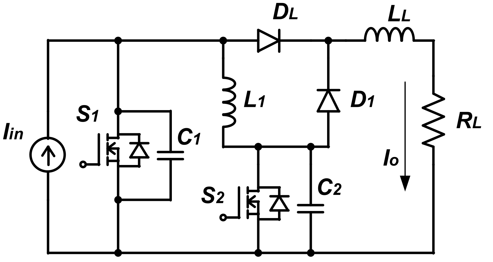
Figure 1 and
Figure 2 show the basic topology proposed for the 1/2 type and −1 type of the switched-inductor power converter (SIPC) with a conversion ratio of 1/2 and −1, respectively. Without
C1 and
C2, it is simply a switched-inductor converter [
19]. The converter is current based and, therefore, there is no output capacitor and only an output inductor. The present design is to add a small capacitor in parallel with the switching devices
S1 and
S2 to create a zero-voltage switching for reduction of switching loss. This is also known as soft-switching because the voltage is during the switching transition is zero and it is preferred switching method [
26].
C1 and
C2 are designed specifically so that it can activate the zero switching in a resonant manner and does not affect the current conversion characteristics of switched-inductor converter. The size of
C1 and
C2 is small, and usually, the multi-layer high-stability version can be used. The topology is also in duality to the switched-capacitor power converter (SCPC) and its resonant version [
7], which has a series inductor, instead, to connect with the transistor under zero current switching. Switched-inductors
L1 and
L2 are assumed to be large such that their ripple is negligible.
S1 and
S2 are turned on and off alternatively in a period with each turn-on time slightly higher than the 50% duty ratio. The overlapping of the turn-on time is a characteristic of current source circuits, and it ensures there is continuous current for the current source that is in duality to the dead-time in the voltage source system. It eliminates any incident of high voltage spike due to discontinuous conduction of input current
Iin by
S1 or
S2.
3. Generalization of Proposed Converters
The proposed power converter is named as a step-down resonant switched-inductor converters (SDRSIC), as shown in
Figure 3. It is obvious a current power converter that provides output to input conversions of 1/3, 1/4, and 1/
n as illustrated in
Figure 3a–c, respectively. The generation skill used here is by a generalized cell that gives the extension to the fractional current divider. A similar inductor and capacitor connection method can also be seen in [
27].
Figure 4 shows the switching cell to generate the
n-order. For
n-order, there are
n−1 switched inductors,
L1 to
Ln−1 plus one
LL to present the load; two diodes
Dna and
Dnb for paralleling
Ln with other switched inductors and two diodes
D(n−1)b and
Dnb for series connection of
Ln with others inductors for discharging and charging operations of
Ln, respectively.
LL together with
RL is to represent the current mode or inductive load. If the load is a current sink,
LL can be taken away. The size of
LL is not critical for the circuit.
The current divider from the input current is through the switching cells. Using 1/n type as an example, the current passes Ln through D(n−1)b and Dnb with other switching inductor cells during its series forward operation, and the currents of all inductors L2 to Ln−1 through D2a and D2c to D(n−1)a and D(n−1)c are summed together for parallel operation. D1a and D(1n−1)c are not needed for simplicity. That is to say, the switched inductors L1 to Ln−1 are for conducting the input current together in parallel and then all the inductors connected in series for releasing the current to load in the next half-cycle. The diodes govern the connection of the inductors in parallel or in series during charging and discharge, respectively.
The non-inverting resonant switched inductor converter has a conversion ratio of 1/(
n−1), with
n being the number of inductors.
Figure 5 shows the inverting circuit for (a) −1/2 type, (b) −1/3 type, and (c) −1/
n type. The inverting resonant switched inductor converter has a conversion ratio of −1/
n with
n inductors.
LL is an inductor to represent the current sink and smoothing of output current but is not a switched inductor.
The technical analysis is conducted below using the idealized analysis. It is assumed that there is no voltage drop on the diodes. The small overlapping time is not considered as they are usually very small as compared with the period and the switching signal duty ratio. The active switches operate with open-loop control at 50% duty cycle. The above assumption is to make the reader understand the basic principles of the proposed circuit series without the influence of the 2nd order effect. The output load is represented by resistor RL. The input side is a constant current source and all switching devices are ideal with no series resistance and on-state voltage.
4. Operational Principles
4.1. Step Down Resonant Converters—Non-Inverting
4.1.1. The Forward (Non-Inverting) Mode 1/3-Type SDRSIC
Four operational stages that depend on the switching states of the transistors are shown in
Figure 6. The operational waveforms, as shown in
Figure 7, are simulated to illustrate each stage. Parameters for the circuit simulation are listed as: inductors
L1 =
L2 = 500 μH, switching frequency
fS = 50 kHz, the resonant capacitor
C1 =
C2 = 0.01 μF, the Load
RL = 8 Ω and the input current
Iin = 6 A. The theoretical simulation waveforms are shown in
Figure 7.
Stage 1 [t0 − t1]: Figure 6a shows the switching states,
S1 is switched off and
S2 is switched on to start the resonance process at
t0.
Figure 6a shows the operation.
L1 and
L2 are in parallel through
S2,
D1c, and
D2a in forward conduction, and
LL through
DL, to carry the input current
Iin. The output is represented by
LL and
RL. The resonant tank is formed by
L1,
L2, and
C1. Voltage on
C1 performs a half-cycle sinusoidal voltage under zero voltage off and on at
t0 and
t1, respectively. Because the switch
S1 is in parallel with
C1, it is under zero voltage switching. It can also be seen that the inductor currents
iL1 and
iL2 swing from minimum at
t0 to maximum values at
t1. Energy is transferred from the source to the inductors.
The state equation is as follows.
where
iL1 and
iL2 are the current through
L1 and
L2, respectively.
The solution of (1) is then:
Then the solution is derived as
where
,
L1 =
L2.
Stage 2 [t1 – t2]:Figure 6b shows the switching states,
S1 is still switched off and
S2 is still switched on, but the resonance process has ended. The voltage on
C1 has completed a half-cycle sinusoidal voltage and continues to be zero from
t1 and
t2.
iL1 and
iL2 remain unchanged. The state equation is
Stage 3 [t2 – t3]: S1 is turned on at
t2 and its voltage is still zero and hence it is under zero voltage switching.
S2 is turned off and its parallel capacitor
C2 starts resonance with
L1 and
L2 connected in series as seen in
Figure 6c, therefore,
S2 is under zero voltage switching. The load is represented by
RL and
LL. The resonant current through
iL1 and
iL2 decreases from maximum to minimum. The resonant voltage across
S2,
vS2, is a sine wave resonance that swings from zero to maximum then back to zero in half a resonant cycle.
The time derivate of
iL1 and
vS2 is
Combines Equations (7) and (8) to give
Then the solution is
where
,
,
L1 =
L2.
Stage 4 [t3 − t4]: Between
t3 and
t4, the switching states of
S1 and
S2 are unchanged. The amplitudes of voltage and current for passive components are also unchanged because the resonance among
C2,
L1, and
L2 has already terminated. The amplitudes of
vS2 and
iL1 are then
During this stage, the load current is provided by the input current as well as the inductors L1 and L2.
4.1.2. Steady-State Equations of 1/3 Type SDRSIC
The input current
and the output current
can be examined by the continuity of the DC part of
iL1. Equating (5) and (11),
It follows that the current conversion relationship becomes
It is noted that the derivation of the conversion ratio is, in fact, independent of the resonant waveforms and the DC components manifest the conversion ratio.
By using input and output power balancing:
The values of voltages
and
can be solved
where
Ts is period of the switching frequency,
T1 and
T2 are the resonant cycles related to
ω1 and
ω2, respectively
To conclude, the amplitude of the key parameters of current and voltage of the resonant components for 1/3 type SDRSIC is
For
Stage 1 [t0 − t1]:
where,
,
,
C1 =
C2,
L1 =
L2.
For
Stage 3 [t2 − t3]:
where
,
C1 =
C2,
L1 =
L2.
4.1.3. General Formulation to 1/n-Type SDRSIC
The general equation of the converter family for type 1/n is described below. It can be deduced that there are (n − 1) switched inductor cells. The description for inductors L1, L2, L3, …, Ln is denoted by , …, , respectively.
For
Stage 1 [t0 − t1]:
where,
,
,
C1 =
C2 =
C,
L1 =
L2 =
L3 = … =
Ln−1 =
L.
For
Stage 3 [t2 − t3]:
where
,
C1 =
C2 =
C,
L1 =
L2 =
L3 = … =
Ln−1 =
L.
The switched-inductors are not needed to be exactly equal to the current sharing. The inductors are connected in both series and parallel in a different stage of operation and, therefore, the small variation in the tolerance does not affect the operation. Again, from the Equations (1) to (25), L1 and L2 do not affect the DC level of the current and hence any tolerance in L does not affect the DC level and the assumption of L1 = L2 is justified.
4.2. SDRSIC—Inverting Design
4.2.1. The Operation Mode 1/2-type SDRSIC
There are four stages of operations, and the equivalent circuit of each stage is shown in
Figure 8. The waveforms of each stage of operation, as shown in
Figure 9, have been illustrated in simulation, which was based on the parameters
L1 =
L2 = 500 μH,
fS = 50 kHz,
Iin = 6 A.
Stage 1 [t0 − t1]: S1 is switched off and
S2 is turned on, both at
t0. The circuit is shown in
Figure 8a to illustrate the equivalent operation.
L1 and
L2 are now in parallel connection through
D1c and
D2a, respectively, and their summed currents are through
S2. If
L1 =
L2, their currents share equally the input current
Iin. The resonance tank is formed by
C1, and
L1 //
L2 The resonant currents
iL1 and
iL2 increase to a maximum after half a resonance cycle, whereas
C2 resonates sinusoidally from zero, swings to maximum and returns to zero.
DL conducts I
o and freewheels the current through
LL and
RL.
The state equations of
vS2,
iL1, and
iL2 are
Equation (26) are using the assumption of
L1 =
L2 to get
iL1 =
iL2. Assuming
(27) and (26) are reduced to:
Then the solution is derived as
where,
,
,
C1 =
C2.
Stage 2 [t1 − t2]: The switching state of
S1 and
S2 remains the same as Stage 1. The equivalent circuit
Figure 8b illustrates the operation. The resonance on capacitor
C1 terminates due to the body-diode of
S1. The currents through
L1 and
L2 are kept at maximum throughout the period
t1 to
t2.
DL freewheels the load current
Io.
The amplitudes of
vS1 and
iL1 are
Stage 3 [t2 − t3]: This is another half cycle resonance when S1 is turned on and S2 is turned off. The resonant tank formed by C2 and series connection of L1 and L2. The voltage across C2 increases in a sinusoidal manner from zero and swings back to zero at t3 after half a resonant cycle. At the same time, the energy stored in inductors L1 and L2 is delivered to load RL. The current direction in RL is in −Io direction
The state equations of
C2,
L1, and
L2 are
Then the solution is
where
,
,
C1 =
C2.
Stage 4 [t3 − t4]: The transistor
S1 continues to be on and
S2 is still off. The resonance of
C2 stops and its voltage has swung to zero. For the duration
t3 to
t4,
iL1 and
iL2 have resonated to their lowest values and remain unchanged for the duration
t3 to
t4. The output current
Io and the ripple
Vy/
Z2 is supported by
iL1. The state equation is
4.2.2. Generalization of Steady-State Solution of Inverting 1/2 Type SDRSIC
The dc portion of the current in inductor
L1 as seen in (30) and (36) are continuous, i.e., the relationship input current
and the output current
is
Because of the power conservation,
The amplitude for switch voltages
Vx and
Vy can be solved
where
Ts is the period of the switching frequency,
and
are the period of resonant frequency for
ω1 and
ω2, respectively.
Finally, the general equations of −1/2 type SDRSIC are now:
For
Stage I [t0 − t1]:
where,
,
,
C1 =
C2,
L1 =
L2.
For
Stage III [t2 − t3]:
where
,
.
4.2.3. General Formulation to 1/n-Type SDRSIC
The generalized form of the inverting-type SDRSIC is shown in
Figure 5c. The individual current of inductors
L1,
L2,
L3, …,
Ln is denoted by
, …,
, respectively. The number of switched-inductor needed is
n and the equations for this generalized topology can be written in terms of
n as follows:
For
State 1 [t0 − t1]:
where,
,
,
C1 =
C2 =
C,
L1 =
L2 = … =
Ln =
L.
For
Stage 3 [t2 − t3]:
where
,
.
5. Example of Circuit Design
To further demonstrate the proposed circuit series, the design of an SDRSIC is shown in the following as an example to illustrate the application. The methods shown below are based on the equation of the resonant components, zero-voltage switching criteria and the resonant voltage equation. It is also a generalized method and can be applied to other switching of frequency and ratings.
- (1)
The proposed circuit is with the following parameters: Iin = 6 A Conversion ratio Io/Iin = 1/3 switching frequency fs = 50 kHz.
- (2)
The next step is to calculate resonant frequency
ωo. The switching cycle is needed to ensure that both resonant tanks derived by resonant frequencies
ω1 and
ω2 can complete the half cycle. Since
ω1 >
ω2. and therefore, to ensure that the zero-voltage switching can be guaranteed,
ωs >
ω2 is a sufficient condition [
24]. Around 10% is selected for their difference:
10% is usually good enough for most of the component’s tolerance in L1, L2, C1, and C2.
- (1)
The impedance defines the ripple on the inductor. A small ripple of 5% as compared to its DC value is used in the design. Equations (11) and (17) give the ripple equation:
where,
, hence, it gives
Z2 = 288 Ω.
- (2)
The L and C values of the resonant tanks are calculated by impedance equations and gives:
L1 = L2 = L = 0.42 mH
C1 = C2 = C = 0.01 μF
0.01 μF and 0.5 mH are used in the circuit prototype. In the circuit, the L1 and L2 are of less current than the input, the inductor used is RM12 of effective volume 8320 mm3. The output inductor is of a similar current; the same size is used for simplicity.
- (3)
The load is represented by a resistor with LL that is large to be regarded as a current sink.
- (4)
The switching devices’ rating voltage is derived from the amplitude of Vx and Vy. Using Equations (16) and (17), Vx = 28.8 V, Vy = 28.8 V. 100 V devices are selected for the prototype.
- (5)
The current passing through the switching devices
S2 is equal to its production summation of duty ratio and the summation of the inductor current during Stage 1 and 2:
where
d is the duty ratio and its equal to 0.5, therefore, the average current passes through the switching devices is 2 A.
- (6)
The current passing through switching device
S1 is shown in stage 3 and 4. Its current is the difference between the input current and inductor current
Therefore, the average current of S1 is then 2 A.
- (7)
The voltage ratings of the diodes are obtained by their voltage impressed to them during the off-stage. This can be deduced from
Section 4. The voltage rating of
D2b,
DL,
D1c, and
D2a are, respectively:
- (8)
The current ratings of the didoes are deduced from their average current and are shown below:
6. Experimental Results
The above converter was constructed to verify the proposed theory. The Bill of Materials (BoM) for the experiment is as follows:
L1 = L2 = LL = 0.5 mH, C1 = C2 = 0.01 μF, D1 = D2 = 45 V 16 A Schottky, S1 and S2 = 100 V 10 mΩ Mosfet.
The inductors were constructed using the conventional high-frequency inductor method on ferrite cores [
28]. The capacitors are polypropylene capacitors. The semiconductors are using a higher current rating for better thermal performance in order to produce a close to the idealized test. The test waveforms of the prototype are shown in
Figure 10. Again, a small overlapping, as illustrated in
Figure 10a, between the two gate signals to
S1 and
S2 are needed for the current source application. There is no voltage spike during the switching of
S1 and
S2 because the resonant switching has been applied through the parallel connection of two resonant capacitors
C1 and
C2 to
S1 and
S2. The resonant voltage across the
S1 and
S2 is in a sinusoidal manner to create the zero-voltage switching, as seen in
Figure 10b. The voltage waveforms show that the voltage across the Mosfet
VS1 and
VS2 are turned on and turned off under zero voltage. The voltage of
S1,
VS1, is the same as the input voltage.
Figure 10c,d shows the inductor currents
iL1 and
iL2 and output current
Io. The current through
L1 and
L2 is 1/3 of
Iin. Overall the results agree well with the theoretical prediction.
The experimental circuit of the converter was tested with various load conditions. The setup of the testing was simple, as the power current was a bench power supply with a current mode setting. The load was constructed by an inductor in series with a resistor that was current sink load and was in duality to a capacitor in parallel with a resistor for voltage output load.
The conversion ratio and the efficiency with load are shown in
Figure 11. The conversion ratio varied around 0.333 and 0.315 when the load changed from 1 to 5 Ω that only slightly drops from idealized 1/3, and is also a common loading effect of power converters, as shown in
Figure 11a. The Mosfet loss was less significant and the diode loss was more significant during light load.
Figure 11b shows the efficiency. Maximum efficiency of 96% is measured at a heavy load of 5 Ω. The converter is the resonant version and the soft-switching further reduces the switching loss and voltage transient. For the current source converter, a load with higher resistance gives higher power because the output power is given by
I2R instead of
V2/
R. Higher
RL or high output power usually implies higher efficiency. It is expected that at a very light load, the conversion ratio is 1/3, and the efficiency is getting lower further. The experimental results have also been compared with the simulation, as shown in
Figure 7. The maximum voltage impressed on the switches is represented by
VS2, which is 24.5 V which is the same as the experimental results. The switched-current on
L1 and
L2 were both varied between 2.05 A and 1.925 A with a mean of 1.99 A. This was the same as the experimental measurement of
iL1 and
iL2, as shown in
Figure 10c.
The photo of the prototype is shown in
Figure 12. It can be seen that the size of the inductor and the semiconductors of the circuit. The resistors are gate driver resistors. The resonant capacitors are small and are soldered under the PCB and tightly connected to the Mosfet.
7. Comparison with Voltage Mode Converters
7.1. Loss Analysis
The next analysis was to examine the performance of the proposed converter as compared with others. The proposed current converter was now compared with other voltage converters using the same conditions as shown in
Section 5, i.e., they were all in the same input voltage, current, power, and also switching frequency, a conventional switched-capacitor resonant step-up converter (SWRSUC), as shown in
Figure 13, of step-up voltage conversion ratio of 3 [
29] was used for the comparison. The same operation condition and criteria, including the switching frequency, were used. The output ripple was set at 5% of the DC average of the output. The equivalent current conversion is then 1/3. Both converters used two transistors and four diodes. SWRSUC used one resonant inductor and four capacitors, whereas the proposed SDRSIC converter used two resonant capacitors and three inductors. Therefore the component count between both converters was similar. The power losses between the two power converters were compared and are shown in
Figure 14. The classical boost converter was also included as a reference. The two converters under comparison are using voltage conversion of three, and hence, their current conversion ratio was 1/3, therefore, the comparisons were based on a fair manner with the same current and voltage conversion ratio, and the same current, voltage, and power. The switching loss exists in the Boost converter, but not the other two converters because soft-switching is used for SWRSUC and SDRSIC. The conduction loss for diode loss is higher in the proposed SDRSIC because the multiple diodes were used for parallel and series arrangement of the switched-inductors, however, it had much less transistor loss because it conducts less switched-inductor current. The inductor loss of SDRSIC was low because of low resonant amplitude and lower DC current. The 1/3 current ratio in this converter made each inductor lower loss and the inductance was small, whereas the conventional boost converter had a large inductor and also its current was large. Although even three inductors were used, the total size for inductors was small but compatible with the conventional boost converter. Because the resonant method is used, the potential for even high power density is promising. The capacitor loss was also low because the capacitor was only used for resonance and its size was small, whereas, for the boost converter and SWRSUC, the capacitors were for main energy storage with larger size and induced higher loss. The overall loss of the proposed converter was less as compared with SWRSUC and the classical boost converter.
The power loss of the proposed converter is independent of the switching frequency because zero-voltage switching is used. However, there was still a certain loss due to the high-frequency loss in the wiring and reactive components. The present design was catered for hundreds of kHz. The loss will be significant when the converter operates beyond MHz.
7.2. Power Density Analysis
It is interesting to compare the power density of the proposed converter with the switched-capacitor resonant converter and the conventional boost converter. The use of inductors for switched-inductor resonant converters as the energy storage is controversial. The analysis is mainly to estimate energy storage in L and C. The other components, such as semiconductors, are relatively small when surface-mount versions are used and are ignored in the following calculation.
The calculation is based on the three converters proposed in the loss analysis above. The L and C for the switched-capacitor resonant converter are designed according to Ref. [
30], and the design of the L and C for boost converter is based on the classical ripple equation [
30].
Table 1 shows the L and C parameters and their side.
The power density is, therefore, as shown in
Table 2:
It can be seen that the proposed switched-inductor resonant converter has the highest power density. Although the power density is not very high as compared with other latest literature, the switching frequency for the present converter is just 50 kHz. The converter is able to work at a higher frequency because of the resonant characteristics, hence, it is expected the power density of the proposed converter increases with the switching frequency. It has a high potential for higher power density frequency.
To compare with the switched-capacitor resonant converter, its capacitor size is large because the electrolytic capacitor cannot be used for high-frequency operation. Only polyester or polypropylene type can be used. The overall size is then large. The boost converter’s power density is between that of the other two converters because it only needs one capacitor and one inductor. However, its potential for further increase in power density using a higher switching frequency is not possible due to its hard switching.
8. Discussion
Switched-inductor converters are an alternative method of power conversion that uses inductors only as the power converter energy storage components. The current conversion ratio is a fraction. The step-down version proposed here has been examined and verified for its power conversion. Both non-inverting and inverting types of operation have been examined. Using an additional resonant capacitor has been proven to reduce the switching transient and is in a soft-switching mechanism. To extend and generalize the techniques, a generation cell is illustrated for 1/n-order conversion development. The paper presents a new method of current conversion using switching cells instead of current-mode control. The mathematics developed is beautiful using the resonant analysis and matches well in power conversion, resonant states, and steady-state. The key contribution is to promote a current-mode power converter and its duality method of generation. A new concept of switching inductors with soft-switching and its generalized equations of the 1/n-order circuits are proposed. The switching is conducted under zero-voltage switching for loss improvement. The loss comparison among other classical switched-capacitor under-voltage modes and the classical boost converter is made. A preferable low loss feature is found in the proposed converter.
The converter finds its potential in the current drive, including the current settings to the charger for battery systems. Different C-rate charging can be realized by the proposed circuit. The proposed converter has a future variation in coupling inductor and tapped inductor to enrich the future switched-inductor design such that switched-capacitor design cannot. Another application is the connection to the PV units that is a current-source. PV has extensive application in the feed-in tariff that increases its installation widely. The current output can therefore be converted to other ratios easily using the proposed technology. Even the battery charger is a current source. The proposed converters work well with the current load. Energy storage such as magnetic energy storage is current-based. The high flux density magnetic devices are emerging, so the energy storage design of the inductor is now higher than a capacitor. The lifetime of inductive energy storage is usually higher than capacitive devices. The preparation of the next era of current-mode power conversion is needed. Also, the breakdown in capacitors is much easier than inductive. For component recycling, the inductor is much easier than the capacitor near the end of life. Therefore there is a high potential for more inductor/current-based conversion in the future and its research work should be well prepared.
9. Conclusions
A current-mode switched-inductor circuit family has been presented and possesses the resonant soft-switching feature. The family consists of step-down, step-up, and inverting power conversion. The work proposed in the paper has presented the principle, operation, and series of circuits. It has come with equations, formation, design methods, and a number of modes of operations. The experimental results confirm the operation and proof of the concept. It also shows the readers the deadtime needed for the current mode. The presented material is a good tutorial paper as well as a good practical research paper.
Author Contributions
Conceptualization, K.W.E.C.; methodology, C.X.; experiment, C.X.; validation, C.X; formal analysis, C.X.; investigation, C.X.; resources, K.W.E.C.; writing and editing, C.X. and K.W.E.C.; supervision, K.W.E.C. and C.X.; project administration, C.X. and K.W.E.C.; funding acquisition, K.W.E.C. All authors have read and agreed to the published version of the manuscript.
Funding
This research was funded by the University Grants Committee General Research Grant, Hong Kong, under grant PolyU 152218/19E.
Institutional Review Board Statement
Not Applicable.
Informed Consent Statement
Not Applicable.
Conflicts of Interest
The authors declare no conflict of interest.
References
- Chen, D.; Jiang, J.; Qiu, Y.; Zhang, J.; Huang, F. Single-Stage Three-Phase Current-Source Photovoltaic Grid-Connected Inverter High Voltage Transmission Ratio. IEEE Trans. Power Electron. 2017, 32, 7591–7601. [Google Scholar] [CrossRef]
- Tran, V.T.; Nguyen, M.K.; Choi, Y.O.; Cho, G.B. Switched-Capacitor-Based High Boost DC-DC Converter. Energies 2018, 11, 987. [Google Scholar] [CrossRef] [Green Version]
- Chen, J.; Wang, C.; Li, J. An Input-Parallel-Output-Series Switched-Capacitor Three-level Boost Converter with a Three-Loop Control Strategy. Energies 2018, 11, 2631. [Google Scholar] [CrossRef] [Green Version]
- Khodaparast, A.; Azimi, E.; Azimi, A.; Adabi, M.E.; Adabi, J.; Pouresmaeil, E. A New Modular Multilevel Inverter Based on Step-Up Switched-Capacitor Modules. Energies 2019, 12, 524. [Google Scholar] [CrossRef] [Green Version]
- Taghvaie, A.; Adabi, J.; Rezanejad, M.A. A Self-Balanced Step-Up Multilevel Inverter Based on Switched-Capacitor Structure. IEEE Trans. Power Electron. 2018, 33, 199–209. [Google Scholar] [CrossRef]
- Duong, T.D.; Nguyen, M.K.; Tran, T.T.; Lim, Y.C.; Choi, J.H. Transformer-Less Switched-Capacitor Quasi-Switched Boost DC-DC Converter. Energies 2021, 14, 6591. [Google Scholar] [CrossRef]
- Da Silva, R.L.; Lazzarin, T.B.; Barbi, I. Reduced Switch Count Step-Up/Step-Down Switched-Capacitor Three-Phase AC–AC Converter. IEEE Trans. Ind. Electron. 2018, 65, 8422–8432. [Google Scholar] [CrossRef]
- Fong, Y.C.; Cheng, K.W.E.; Raman, S.R.; Wang, X. Multi-Port Zero-Current Switching Switched-Capacitor Converters for Battery Management Applications. Energies 2018, 11, 1934. [Google Scholar] [CrossRef] [Green Version]
- Berkovich, Y.; Axelrod, B.; Madar, R.; Twina, A. Improved Luo converter modifications with increasing voltage ratio. IET Power Electron. 2015, 8, 202–212. [Google Scholar] [CrossRef]
- Amjadi, Z.; Williamson, S.S. A Novel Control Technique for a Switched-Capacitor-Converter-Based Hybrid Electric Vehicle Energy Storage System. IEEE Trans. Ind. Electron. 2010, 57, 926–934. [Google Scholar] [CrossRef]
- Müller, L.; Kimball, J.W. A Dynamic Model of Switched-Capacitor Power Converters. IEEE Trans. Power Electron. 2014, 29, 1862–1869. [Google Scholar] [CrossRef]
- Fardahar, S.M.; Sabahi, M. New Expandable Switched-Capacitor/Switched-Inductor High-Voltage Conversion Ratio Bidirectional DC–DC Converter. IEEE Trans. Power Electron. 2021, 35, 2480–2487. [Google Scholar] [CrossRef]
- Stauth, J.T.; Seeman, M.D.; Kesarwani, K. Resonant Switched-Capacitor Converters for Sub-module Distributed Photovoltaic Power Management. IEEE Trans. Power Electron. 2013, 28, 1189–1198. [Google Scholar] [CrossRef]
- Yuanmao, Y.; Cheng, K.W.E. Level-Shifting Multiple-Input Switched-Capacitor Voltage-Copier. IEEE Trans. Power Electron. 2012, 27, 828–837. [Google Scholar] [CrossRef]
- Ye, Y.; Cheng, K.W.E. Multi-Port Voltage-Subtracting Circuit Based on Resonant Switched-Capacitor. IET Power Electron. 2012, 5, 693–701. [Google Scholar] [CrossRef]
- Tanaka, Y.; Iseki, H. Switched Capacitor Rectifier Circuit; U.S. Patent and Trademark Office: Washington, DC, USA, 1987.
- Yuanmao, Y.; Cheng, K.W.E.; Yeung, Y.P.B. Zero-Current Switching Switched-Capacitor Zero-Voltage-Gap Automatic Equalization System for Series Battery String. IEEE Trans. Power Electron. 2012, 27, 3234–3242. [Google Scholar] [CrossRef]
- Sano, K.; Fujita, H. Voltage-balancing circuit based on a resonant switched-capacitor converter for multilevel inverters. IEEE Trans. Ind. Appl. 2008, 44, 1768–1776. [Google Scholar] [CrossRef]
- Cheng, K.W.E.; Ye, Y.M. Duality Approach to the Study of Switched-Inductor Power Converters and its Higher Order Variations. IET Power Electron. 2015, 8, 489–496. [Google Scholar] [CrossRef]
- Salvador, M.A.; de Andrade, J.M.; Lazzarin, T.B.; Coelho, R.F. Nonisolated High-Step-Up DC–DC Converter Derived from Switched-Inductors and Switched-Capacitors. IEEE Trans. Ind. Electron. 2021, 67, 8506–8516. [Google Scholar] [CrossRef]
- Khan, S.; Mahmood, A.; Tariq, M.; Zaid, M.; Khan, I.; Rahman, S. Rahman: Improved Dual Switch Non-Isolated High Gain Boost Converter for DC microgrid Application. In Proceedings of the 2021 IEEE Texas Power and Energy Conference (TPEC), College Station, TX, USA, 4–5 February 2021. [Google Scholar]
- Bao, D.; Kumar, A.; Pan, X.; Xiong, X.; Beig, A.R.; Singh, S.K. Kumar Singh; Switched Inductor Double Switch High Gain DC-DC Converter for Renewable Applications. IEEE Access 2021, 9, 14259–14270. [Google Scholar] [CrossRef]
- Ye, Y.; Lin, J.; Li, Z.; Wang, X. Double-Tiered Cell Balancing System With Switched-Capacitor and Switched-Inductor. IEEE Access 2019, 7, 183356–183364. [Google Scholar] [CrossRef]
- Tang, Y.; Tong, H.; Afzal, R.; Guo, Y. High step-up ZVT Converter Based on Active switched Coupled inductors. IEEE Access 2020, 1, 1. [Google Scholar] [CrossRef]
- Ohta, M.; Hasegawa, R. Soft Magnetic Properties of Magnetic Cores Assembled With a High BS Fe-Based Nanocrystalline Alloy. IEEE Trans. Magn. 2017, 53, 2000205. [Google Scholar] [CrossRef]
- Leandro, G.M.; Barbi, I. Barbi: Switched-Capacitor LLC Resonant DC-DC Converter With Switch Peak Voltage of Vin/2. IEEE Access 2020, 8, 111501–111513. [Google Scholar] [CrossRef]
- Zhu, X.; Ye, K.; Liu, K.; Zhang, B. Non-isolated High Step-up DC-DC Converter with Passive Switched-Inductor-Capacitor Network. IEEE J. Emerg. Sel. Top. Power Electron. 2021, 1, 1. [Google Scholar] [CrossRef]
- Cheng, K.W.E. Computation of the AC Resistance of Multistranded Conductor Inductors with Multilayers for High Frequency Switching Converters. IEEE Trans. Magn. 2000, 36, 831–834. [Google Scholar] [CrossRef] [Green Version]
- Law, K.K.; Cheng, K.E.; Yeung, Y.B. Design and analysis of switched-capacitor based step-up resonant converters. IEEE Trans. Circuits Syst. I Regul. Pap. 2005, 52, 943–948. [Google Scholar] [CrossRef] [Green Version]
- Cheng, K.W.E. Classical Switched-Mode and Resonant Power Converters; The Hong Kong Polytechnic University: Hong Kong, China, 2002; ISBN 962-367-364-7. [Google Scholar]
Figure 1.
Non-inverting design of half-type resonant switched-inductor converter circuit.
Figure 1.
Non-inverting design of half-type resonant switched-inductor converter circuit.
Figure 2.
Inverting design of resonant switched-inductor converter circuit.
Figure 2.
Inverting design of resonant switched-inductor converter circuit.
Figure 3.
The step-down resonant switched-inductor converters using non-inverting design; (a) 1/3-type, (b) 1/4-type, (c) 1/n-type.
Figure 3.
The step-down resonant switched-inductor converters using non-inverting design; (a) 1/3-type, (b) 1/4-type, (c) 1/n-type.
Figure 4.
Switching inductor cell for fractional conversion generation.
Figure 4.
Switching inductor cell for fractional conversion generation.
Figure 5.
Inverting step down resonant switched-inductor converters; (a) −1/2-type, (b) −1/3-type, (c) −1/n-type.
Figure 5.
Inverting step down resonant switched-inductor converters; (a) −1/2-type, (b) −1/3-type, (c) −1/n-type.
Figure 6.
The operation stages of 1/3-type SDRSIC; (a) Stage 1, (b) Stage 1, (c) Stage 1 (d) Stage 4.
Figure 6.
The operation stages of 1/3-type SDRSIC; (a) Stage 1, (b) Stage 1, (c) Stage 1 (d) Stage 4.
Figure 7.
Simulation of 1/3-type SDRSIC to show the switching states.
Figure 7.
Simulation of 1/3-type SDRSIC to show the switching states.
Figure 8.
The equivalent circuit to show 4 stages for inverting 1/2-type SDRSIC; (a) Stage 1, (b) Stage 2, (c) Stage 3, (d) Stage 4.
Figure 8.
The equivalent circuit to show 4 stages for inverting 1/2-type SDRSIC; (a) Stage 1, (b) Stage 2, (c) Stage 3, (d) Stage 4.
Figure 9.
Theoretical simulation of inverting 1/2-type SDRSIC.
Figure 9.
Theoretical simulation of inverting 1/2-type SDRSIC.
Figure 10.
Measured waveforms for 1/3-type SDRSIC with Iin = 6 A and RL = 3 Ω, (a) Ch1 (B): VGS1; Ch2 (R): VGS2; (b) Ch2 (R): VGS1; Ch1 (B): VS1; Ch3 (G): VS2; (c) Ch1 (top): VGS1; Ch2 (middle): iL1; Ch4 (bottom): iL2; (d) Ch2 (top): VGS2; Ch4 (middle): Iin; Ch3 (bottom): Io.
Figure 10.
Measured waveforms for 1/3-type SDRSIC with Iin = 6 A and RL = 3 Ω, (a) Ch1 (B): VGS1; Ch2 (R): VGS2; (b) Ch2 (R): VGS1; Ch1 (B): VS1; Ch3 (G): VS2; (c) Ch1 (top): VGS1; Ch2 (middle): iL1; Ch4 (bottom): iL2; (d) Ch2 (top): VGS2; Ch4 (middle): Iin; Ch3 (bottom): Io.
Figure 11.
Experimental results of conversion ratio and efficiency of the 1/3 type proposed converter under Iin = 2 A − 6 A; (a) current ratio against output resistance, (b) conversion efficiency against load.
Figure 11.
Experimental results of conversion ratio and efficiency of the 1/3 type proposed converter under Iin = 2 A − 6 A; (a) current ratio against output resistance, (b) conversion efficiency against load.
Figure 12.
The prototype converter.
Figure 12.
The prototype converter.
Figure 13.
The conventional switched-capacitor resonant step-up converter (SWRSUC) used for comparison.
Figure 13.
The conventional switched-capacitor resonant step-up converter (SWRSUC) used for comparison.
Figure 14.
Loss Comparison among different converters.
Figure 14.
Loss Comparison among different converters.
Table 1.
Comparison of converter size and power density.
Table 1.
Comparison of converter size and power density.
| | L | C | L Size (Ferrites or Air Core) | C Size (Polyester) | Total Size |
|---|
| Switched-inductor SDRSIC | 0.42 mH + 0.42 mH | 0.01 μF + 0.01 μF | 8320 mm3 (RM12) + 8320 mm3 (RM12) | 113 mm3 + 113 mm3 | 16,866 mm3 |
| Switched-capacitor SWRSUC | 0.023 μH | 180 μF + 47 μF + 47 uF | 1570 mm3 (air-core) | 72,475 mm3 + 18,924 mm3 + 18,924 mm3 | 111,893 mm3 |
| Boost | 148 μH | 56 μF | 4310 mm3 (RM10) | 21,460 mm3 | 25,770 mm3 |
Table 2.
The power density of the three converters.
Table 2.
The power density of the three converters.
| SDRSIC | SWRSUC | Boost |
|---|
| 1.18 W/cm3 | 0.18 W/cm3 | 0.78 W/cm3 |
| Publisher’s Note: MDPI stays neutral with regard to jurisdictional claims in published maps and institutional affiliations. |
© 2022 by the authors. Licensee MDPI, Basel, Switzerland. This article is an open access article distributed under the terms and conditions of the Creative Commons Attribution (CC BY) license (https://creativecommons.org/licenses/by/4.0/).


