Abstract
Partial discharge (PD) detection can be considered one of the most useful tools for assessing the insulation conditions of the power apparatus in high-voltage systems. Under AC conditions, this analysis is widely employed in online and offline tests, such as type tests or commissioning, and can be carried out by applying the phase-resolved PD (PRPD) method, since the patterns can give information about the defect classification. Under DC voltages, the classic pattern recognition method cannot be performed, and the measurements show complexities related to the nature of the phenomena. For this reason, to date, a standard for PD measurements under DC does not exist. In previous papers, a new method for PD detection under DC stress voltages has been proposed by the authors. It is based on the application of a direct current periodic (DCP) waveform useful in obtaining PRPD patterns. The dependence of partial discharge inception voltage (PDIV) and PD repetition rate (PDRR) on the δ shape parameter of the DCP for different materials, as well as the capability to recognize different discharge phenomena, provided valid indications on the behavior of PD in the transition from AC to DC. The aim of this paper is to evaluate the time dependence of PD occurring in a dielectric by applying the DCP waveform. In our previous studies, the investigations were focused on the PD behavior under different values of the DC voltage periodic part. In another work, the DCP waveform with both positive and negative polarity was applied to several dielectric materials. In the proposed work, instead, the DCP waveform is applied for a long time in order to observe its effect on the PD behavior for 72 h. In this way, due to the space charge accumulation phenomenon, the aging effect, also due to the space charge accumulation phenomenon, is evaluated. The methodological approach was to acquire PRPD patterns over time and evaluate their trends in comparison with the sinusoidal case. The experimental results show that, with a DCP waveform having δ = 0.6, the aging effect similar to that provided by pure DC stress is observed, while the acquired PRPD patterns are easily interpretated, as in the AC case.
1. Introduction
PD measurements are a widespread approach to determine the status of efficiency of insulation systems [1]. In a HVAC apparatus, the defect recognition techniques are typically based on PRPD pattern acquisitions and postprocessing algorithms adopting statistical parameters and neural networks [2,3,4]. Conversely, in HVDC systems, PD measurements are much less standardized, so much so that, often, the standards propose to use AC stresses for the type tests of DC components. In particular, the CIGRÈ Technical Brochure (TB) 496 [5] and the Standard IEC 62895:2017 [6] are the main international standards for testing HVDC cable systems. Both standards prescribe the prequalification and the electrical-type test on entire cable systems. Moreover, they suggest the use of AC stress in order to test components employed in HVDC transmission systems, such as joints. For testing the dielectric of polymeric extruded HVDC cable joints, Mazzanti et al. published two interesting articles on tests for extruded HVDC cable joints [7,8]. In Reference [7], a review focused on typing, the design and testing techniques (especially for PD and space charge measurements) of extruded cable joints are reported in detail.
In Reference [8], instead, a novel protocol for PD measurements during routine tests in HVDC extruded cable joints carried out by means of AC voltages and VHF/UHF electromagnetic wireless sensors was proposed. In summary, the protocol set the calibration of the VHF/UHF sensor, the measurement setup, the measurement procedure and the acceptance criteria.
However, the different solutions reported above do not take into account that DC degradation phenomena under DC are very different from those under AC ones, and the influence of some parameter like space charge diffusion due to the electric field and thermal gradient can reduce misunderstandings and evaluation errors.
The adoption of AC stress for PD tests on components employed in HVDC systems is due to the fact that PD measurements under constant stress waveforms results are complicated. The main causes of these difficulties can be attributed to the nature of PD phenomena under DC stress, as well as to the supply conditions [9].
To overcome the problems described above, in a previous paper, the authors proposed a new stress voltage waveform called DC periodic (DCP), created by the superposition of a continuous component and a sinusoidal one [10,11,12]. In this way, the specimen under testing results were stressed, with a waveform having the same features of the DC voltage. Due to the sinusoidal part of the DCP waveform, the polarization effect increases the PD amount. Moreover, the synchronization of the occurring PD can be carried out, and the PRPD pattern can be obtained; therefore, the recognition techniques suitable under AC stress can be used.
In Reference [10], where the DCP waveform was introduced for the first time, PD measurements were made in only one insulating material and by applying the DCP with only positive polarity. In order to confirm the advantages provided by the new DCP waveform, in another work published by the authors [12], several insulating materials, such as XLPE, PET, Kapton and M.I. paper, were tested. In addition, PD measurements were carried out by stressing the specimens with the DCP in both positive and negative polarity. Additionally, in this case, the measurement results confirmed the good performance of the proposed waveform.
However, in the two previously published articles, the reported PRPD patterns were obtained after a few minutes of the applied DCP stress.
As is well-known, under DC stress, the accumulation of space charge is one of the main degradation phenomena. Furthermore, considering that the availability of a charge is a necessary condition for the PD activity; the two phenomena are closely related.
Based on the above, the aim of the present work is to evaluate the effect (in terms of PD behavior) produced by the DCP waveform applied for a long time on a specimen containing an air void defect. This is in order to evaluate the effect of the DCP on the aging phenomena typically due to space charge accumulation, treeing, cavity erosion, etc.
Unfortunately, the amount of accumulated charge within the air void cannot be directly evaluated. This because the pulsed electroacoustic (PEA) method presents difficulties in the measurement of charges in specimens containing an air layer [13]. Nevertheless, the effect of the DCP waveform on the space charge accumulation phenomenon has already been evaluated in a single-layer specimen [14]. In that work, the authors found that no substantial differences occurred between the charges accumulated under the DCP and those accumulated under pure DC stress.
However, the goal of the present work is to evaluate the effect on PD behavior of the DCP waveform applied for a long time with the aim to confirm, after several hours of applied stress, the advantages provided by the proposed waveform. In particular, the aim of this work is focused on the acquisition of patterns like those obtained under AC voltage but generated with a waveform producing the same effect of DC stress.
This article is structured as follows. First of all, the previously developed DCP waveform is mathematically and graphically described. Then, the arranged measurement setup and the measurement procedure are reported. In the following section, the PRPD patterns obtained under the sinusoidal stress, as well as under two different shapes of DCP stress, are reported and described in detail. Finally, Section 5 collecting the main differences among the obtained PD patterns is reported.
2. Experimental Approach
The adopted waveform was introduced by the authors with the aim of deepening the study of the PD phenomenon under DC.
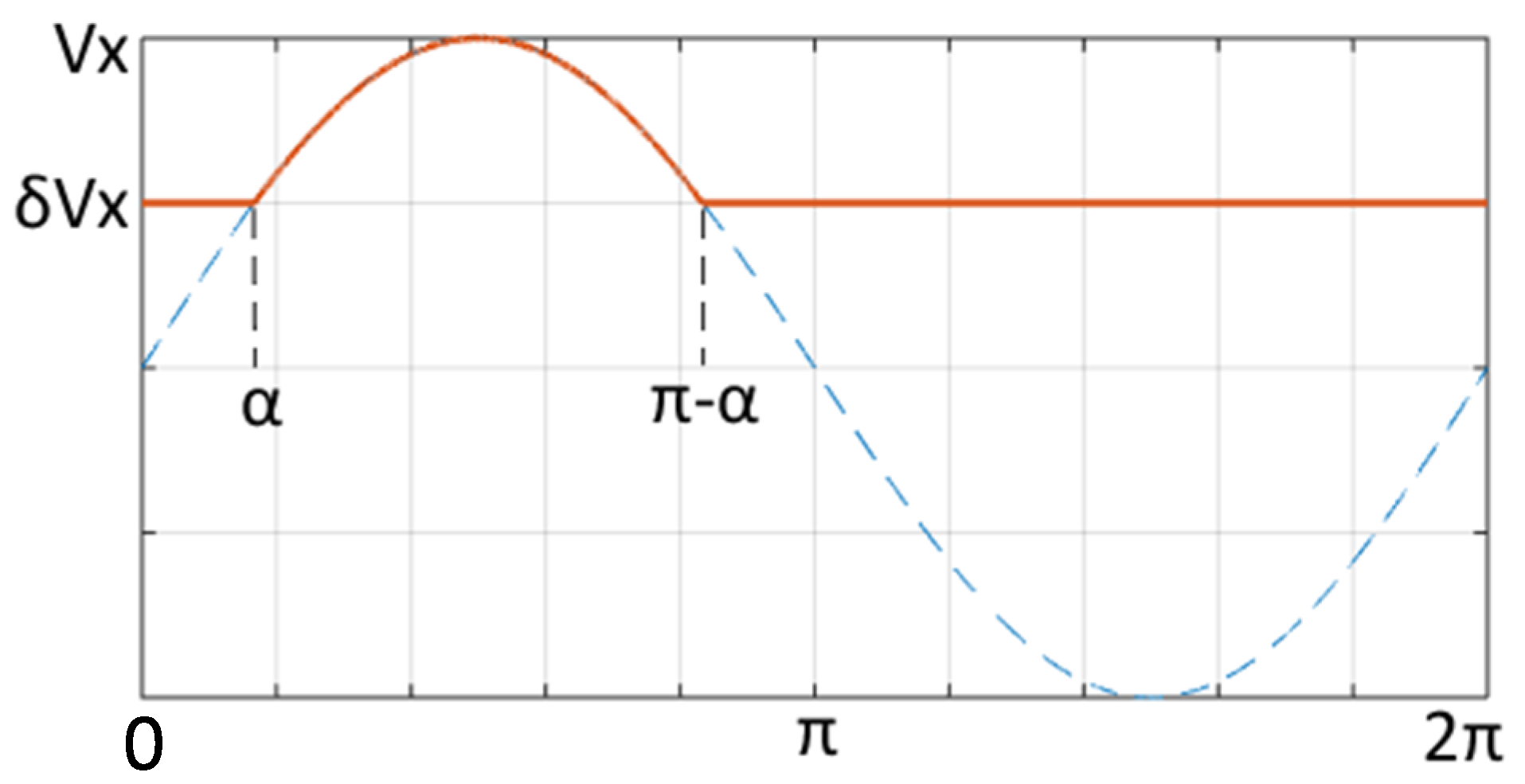
The DCP waveform, fully described in a previous paper [10], comes from the mathematical relationship reported in Equation (1), while Figure 1 shows its shape.
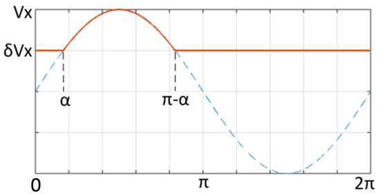
Figure 1.
DCP waveform in positive polarity with the variable δ parameter.
The DCP function is a combination between a constant part and a sinusoidal part. On the basis of a parameter named “delta” (δ), it can transit from a half-wave sinusoid, for δ = 0, to a pure DC waveform for δ = 1.
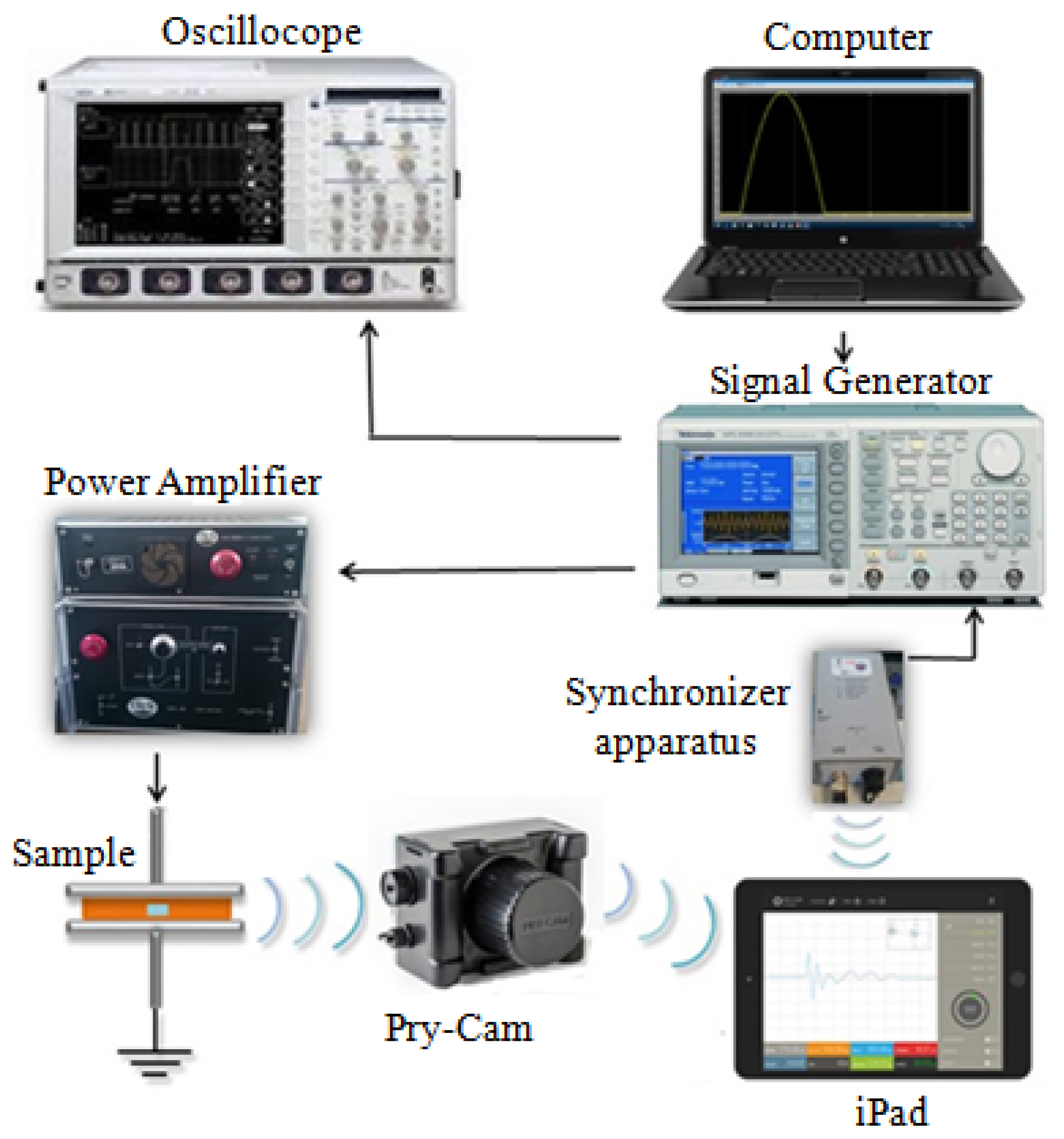
This approach enables having a unipolar waveform whose shape can vary gradually from half-sinusoid to pure DC. Furthermore, the sinusoidal part is the one that allows the discharge synchronization with the phase of the applied voltage and, therefore, the realization of the PRPD pattern [10]. The laboratory setup is schematically reported in Figure 2.
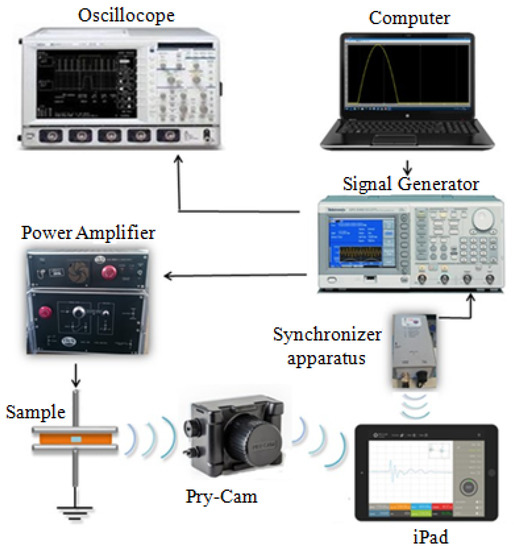
Figure 2.
Laboratory setup for the generation of DCP waveforms and acquisition of PD patterns.
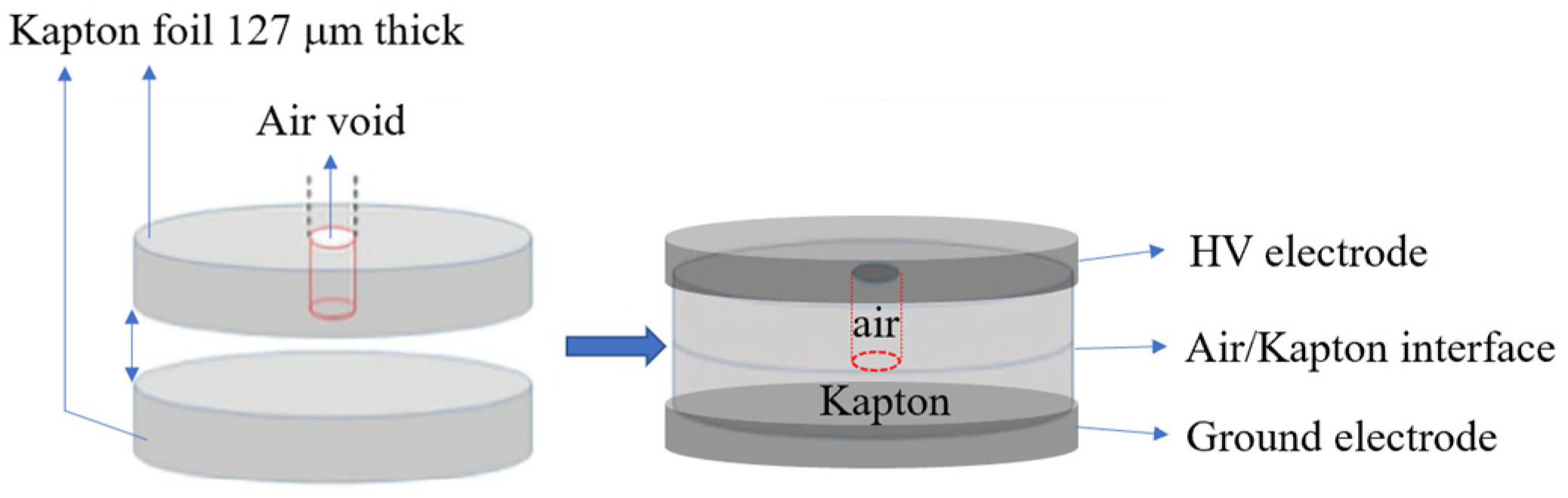
A PC, connected with a Tektronix signal Generator AFG 31000, generates waveforms adopting a MATLAB/Simulink function. Then, the signal is sent to a Trek 662 power amplifier and, subsequently, to a test sample. The selected specimen is a Kapton bilayer with 127-μm thickness each and with a 6-mm circular hole in the upper layer. The material is inserted between two stainless-steel plane electrodes in order to simulate an internal cavity, as shown in Figure 3. The stainless-steel electrodes, made with a radius and a thickness of 30 mm and 7 mm, respectively, have a semicircular smoothed border in order to prevent edge effects. Furthermore, the specimen, with a radius approximately 5 mm wider than that of the electrodes, is immersed in silicone oil to avoid the appearance of corona discharges or partial discharges along the Kapton surface [10].
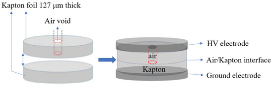
Figure 3.
Specimen under test.
The acquisition of PD was performed by a Pry-Cam® portable instrument Wi-Fi connected with a tablet [15,16]. For all acquisitions, the instrument was placed approximately 20 cm from the earth connection cable, the gain was left constant with a full scale of 245 mV and all acquisitions were stopped after acquiring about 15,000 pulses. The trigger threshold was set at 15.43 mV in order to eliminate the background noise generated by the amplifier [16].
The measurements were aimed to assess the time trend of the PD phenomenon by comparing the results obtained under sinusoidal and DCP waveforms. This verifies the possible influence of aging phenomena on the PD evolution.
The selected DCP for the experimental tests in the present article are characterized by δ = 0 and δ = 0.6. The first value was chosen because it involves a waveform with the highest sinusoidal part, whilst the DCP with δ = 0.6 generates an accumulation of charges similar to that obtained under pure DC stress [12].
3. Experimental Measurements
The experimental measurements addressed the comparison among partial discharge acquisitions performed under pure sinusoidal voltage and the DCP voltages with two different values of δ. The measurement data are shown in Table 1. As can be observed, the pure sinusoidal voltage with a magnitude equal to 4 kV was applied for 24 h, and the detected PDIV resulted in 1.4 kV. Regarding the new waveform, DCP stress with δ = 0 and a magnitude of 4 kV was applied for 24 h, whilst DCP stress with δ = 0.6 and a magnitude of 7 kV was applied for 72 h. All this voltage values are intended as the maximum values. This time was chosen in order to be sufficient to consider space charge diffusion phenomena due to the applied DC voltage and not be too long to be influenced by aging phenomena due to the PD effect. In the latter case, the PDIV was equal to 6 kV. This greater value can be related to the smaller sinusoidal part of the DCP with δ = 0.6 compared to that with δ = 0.

Table 1.
Data measurements.
Once the PDIV for each waveform was determined, obtained by increasing the voltage continuously with a rising rate of about 0.5 kV/s, the measurements were performed with different durations. The experiments lasted 24 h for the AC and δ = 0 DCP tests, whilst the observation was 72 h for the DCP with δ = 0.6. The characteristics of the PD phenomena during the tests can be depicted by the acquisition of the PRPD pattern, the repetition rate in pulse per second (PPS) and the Qmax 95th parameter that is the discharge maximum magnitude where 95% of the discharges are contained.
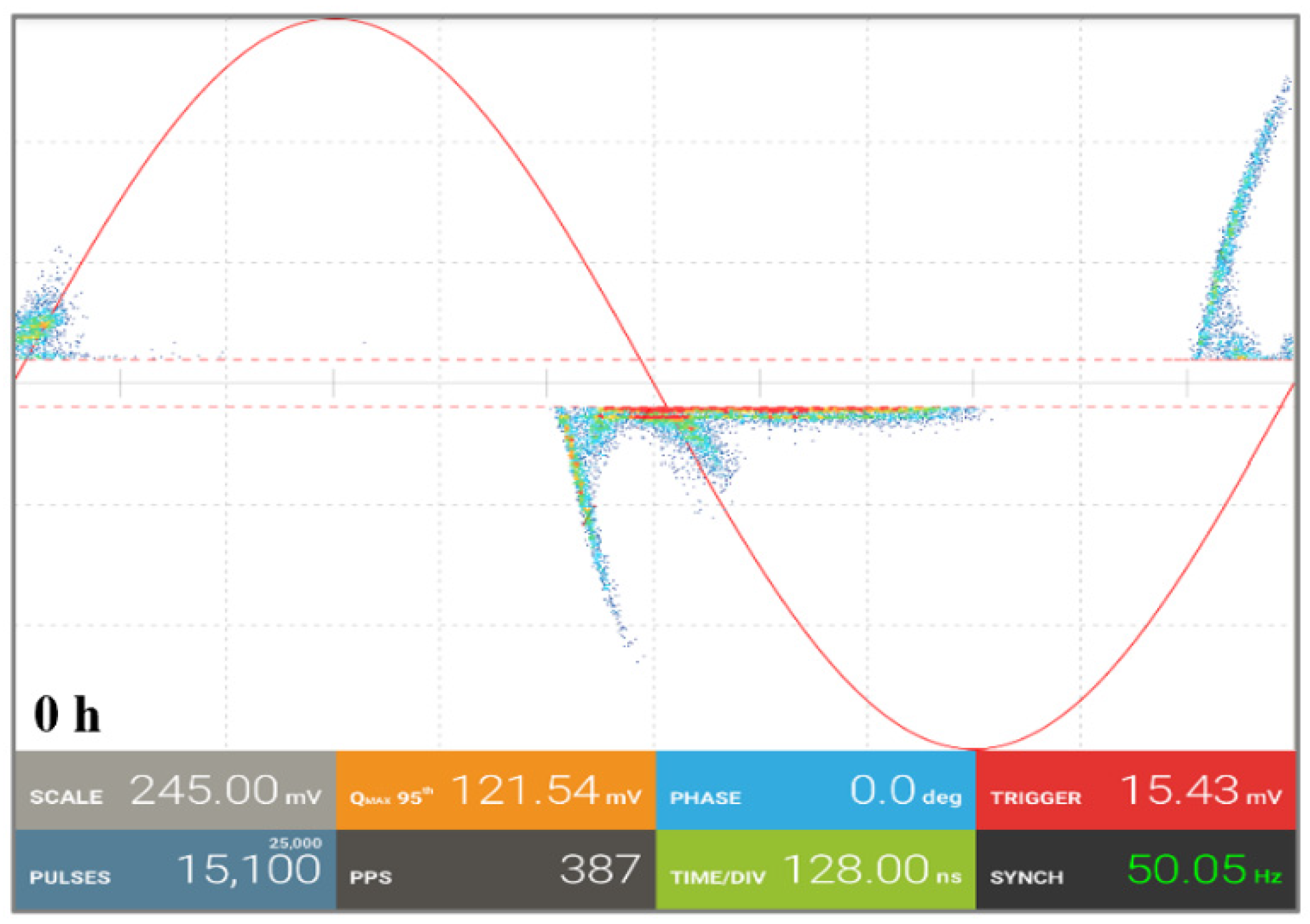
3.1. PRPD Pattern Detected under AC Stress
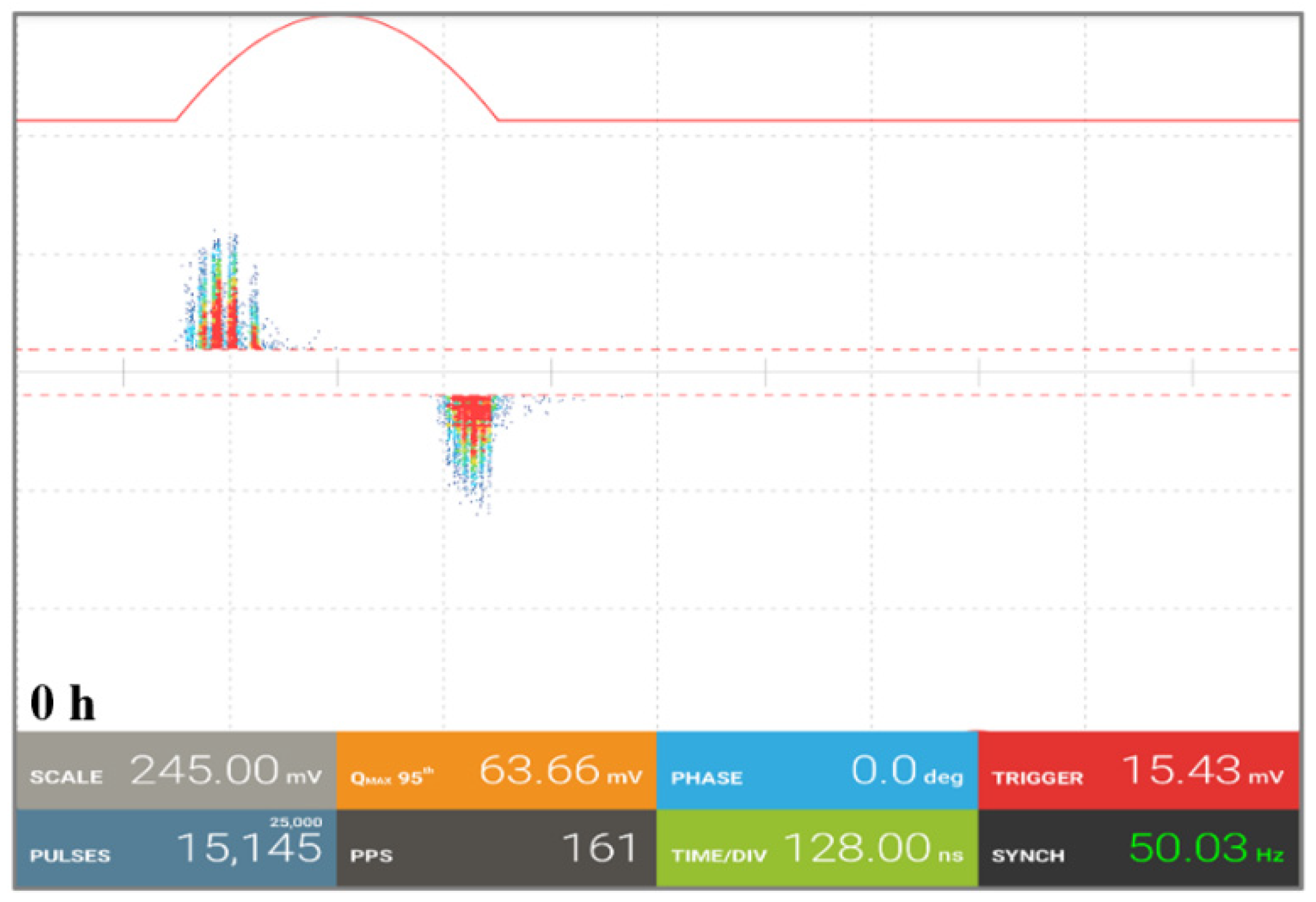
The PRPD pattern trend under the sinusoidal regime, after a few minutes of voltage application, is reported in Figure 4. As can be observed, the PRPD pattern shows a classic “rabbit” internal void behavior with clearly visible ears for both polarity discharges. In the bottom part of Figure 4, the acquisition parameters, such as the scale, the trigger and the time/div, are reported. These values are the same for all acquired PRPD patterns depicted in this article.

Figure 4.
PRPD pattern under AC stress acquired after a few minutes of voltage application.
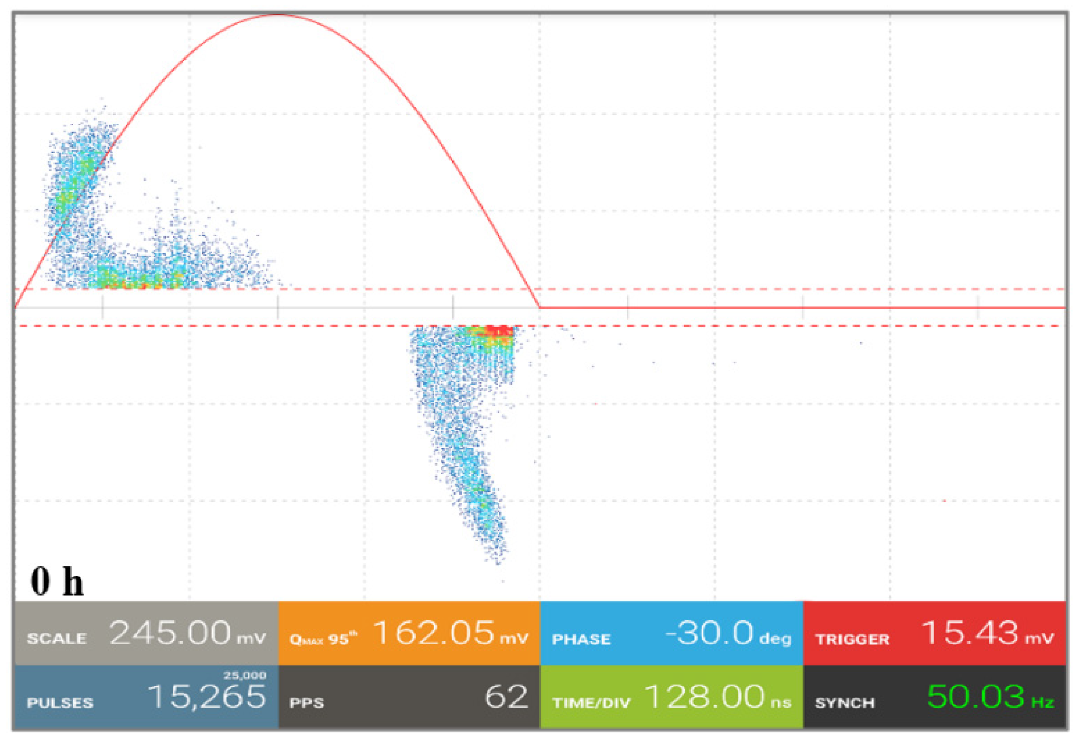
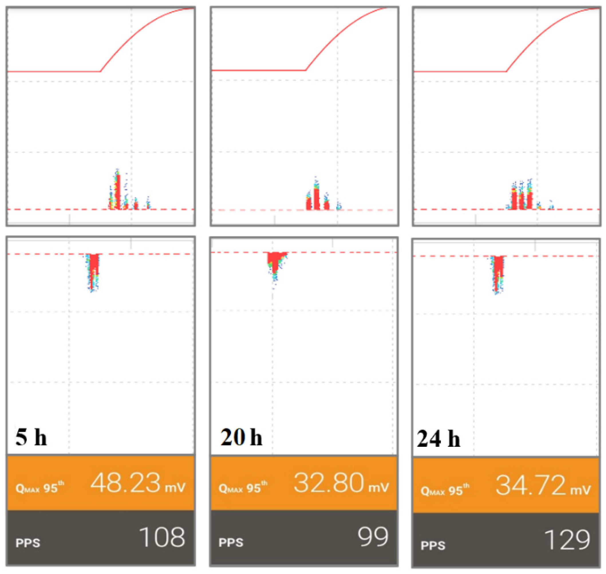
In order to observe the effect of long-term voltage application, the PD activity was monitored for 24 h.
In Figure 5, the PRPD patterns acquired after 5, 20 and 24 h of voltage application are reported. The patterns acquired during the positive half-wave of the sinusoidal voltage are those located in the upper part of the figure. On the other hand, the patterns in the lower part refer to the negative half-wave.
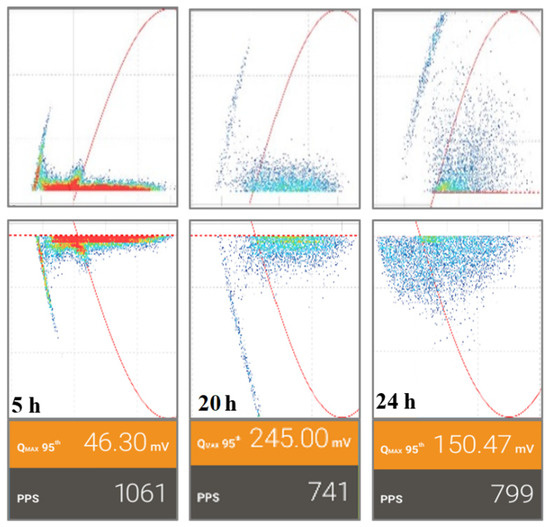
Figure 5.
Sinusoidal voltage PRPD patterns acquired after 5, 20 and 24 h of voltage application. To save space compared to Figure 4, the PRPD patterns positioned in the upper part are referred to as the positive half-wave, whilst those in the bottom part are referred to as the negative half-wave.
The changes over time show an increasing variability, and after 24 h, the trend shows the disappearance of the ear in the discharges of negative polarity.
3.2. PRPD Pattern Detected under the DCP Waveform with δ = 0
Once the reference sinusoidal measurements were performed, PRPD patterns were obtained under DCP waveforms by extracting the patterns from the instrument software and superimposing the discharges with the DCP reference voltage. The detailed description of the waveform behavior was explained in a previous work [10]. The PD acquisition with the DCP parameter δ = 0 after a few minutes of voltage application is shown in Figure 6.

Figure 6.
DCP voltage PRPD patterns with δ = 0, acquired after a few minutes of voltage application.
The measurement results obtained after 5, 20 and 24 h of application of the DCP waveform with δ = 0 are depicted in Figure 7. By observing the PRPD patterns of Figure 5 and Figure 6, it is possible to notice that, at the beginning, the double rabbit ears are present. During the testing time, the rabbit ear shapes remain visible only for the positive polarity of the applied voltage. On the contrary, for the negative polarity, the rabbit ears are significantly reduced. However, a variation during the time of the PRPD pattern from the typical rabbit-like shape to a turtle-like pattern was observed.
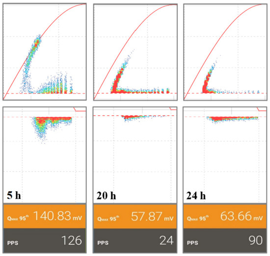
Figure 7.
DCP voltage PRPD patterns with δ = 0 acquired after 5, 20 and 24 h of voltage application. To save space compared to Figure 6, the PRPD patterns positioned in the upper part are obtained during the DCP rising time, whilst those in the bottom part refer to the DCP falling time.
Typically, the transition of the PRPD patterns from rabbit-like to turtle-like is a phenomenon indicating cavity aging (e.g., electrical tree) when a sinusoidal stress is applied for long time [17,18,19]. However, it is important highlight that this phenomenon was also present in our experimental tests, where the DCP waveform was used as the stress voltage. This confirms that the PD behavior and, thus, the detected PRPD pattern obtained with DCP stress does not differ from those related to sinusoidal voltage.
In addition, the more accentuated turtle-like pattern of the negative discharges of Figure 7 after 24 h, like the correspondent negative pattern of Figure 5 when the sinusoidal voltage was applied, means an aging effect provided by the DCP [17,18]. In fact, the DCP waveform containing a DC component leads to a greater accumulation of charge, which is responsible of several factors, namely a different number of free electrons available for the discharge, a different electric field distribution within the air void and an increase in the aging phenomenon.
3.3. PRPD Pattern Detected under the DCP Waveform with δ = 0.6
The last measurement was made by means of the DCP waveform with δ = 0.6. In Figure 8, the PRPD pattern acquired at the beginning from the voltage application is reported. The patterns in Figure 9 were obtained after 5, 20 and 24 h.

Figure 8.
DCP voltage PRPD patterns with δ = 0.6, acquired after a few minutes of voltage application.

Figure 9.
DCP voltage PRPD patterns with δ = 0.6, acquired after 5, 20 and 24 h of applied voltage. To save space compared to Figure 8, the PRPD patterns positioned in the upper part are obtained during the DCP rising time, while those in the bottom part refer to the DCP falling time.
As can be observed, the detected patterns showed a similar rabbit-like shape. Of course, since the DCP waveform with δ = 0.6 has a smaller sinusoidal part, a classic rabbit-like pattern with the same characteristics of those observed under the aforementioned conditions cannot be obtained. As shown in Figure 9, in this case, several differences can be noticed. In particular, the positive PD are lower in magnitude, whilst the pattern referred to as the negative PD does not change from the rabbit-like to a turtle-like shape. However, these differences between the PRPD patterns obtained with two different values of δ are certainly attributed to the DCP waveform. Despite the case with δ = 0, with δ = 0.6, the applied voltage has a smaller sinusoidal part and a greater constant part, which causes a higher PDIV and a different charge accumulation.
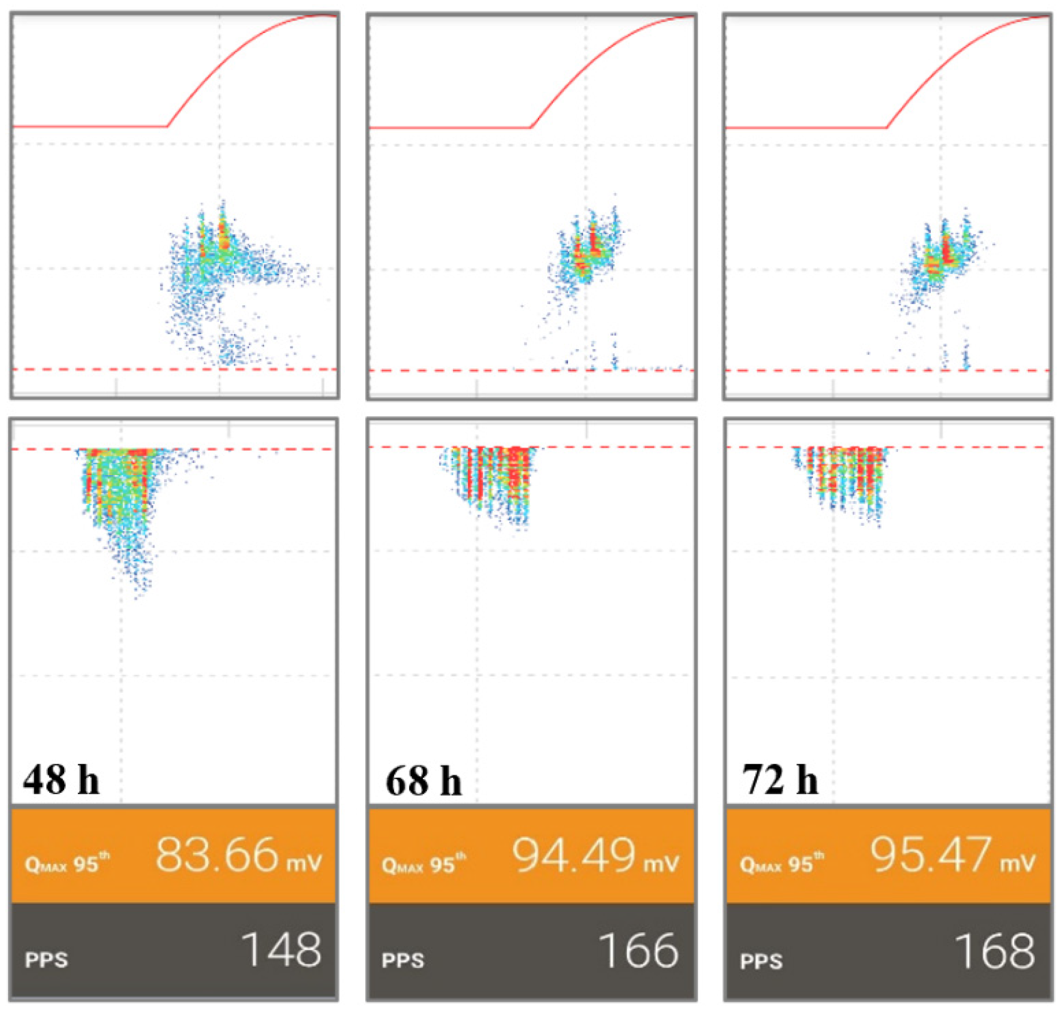
With the aim of emphasizing the aging effect due to the space charge accumulation phenomenon, further PD acquisitions were made at 48, 68 and 72 h. The related PRPD patterns are shown in Figure 10. In this case, the accumulated charge and its distribution over the air void surface are strongly influenced by the long-time DCP stress application.
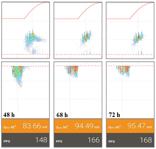
Figure 10.
DCP voltage PRPD patterns with δ = 0.6, acquired after 48, 68 and 72 h of voltage application. To save space compared to Figure 8, the PRPD patterns positioned in the upper part are obtained during the DCP rising time, while those in the bottom part refer to the DCP falling time.
To better understand the patterns of the figure above, the space charge accumulation phenomenon was analyzed.
Certainly, charge detection on the whole sample would have been very useful. Unfortunately, the measurement of space charge in the entire air/Kapton specimen cannot be carried out by means of the pulsed electroacoustic (PEA) method due the air material, which acts as barrier for the acoustic wave and, thus, does not allow the detection of accumulated charges [13].
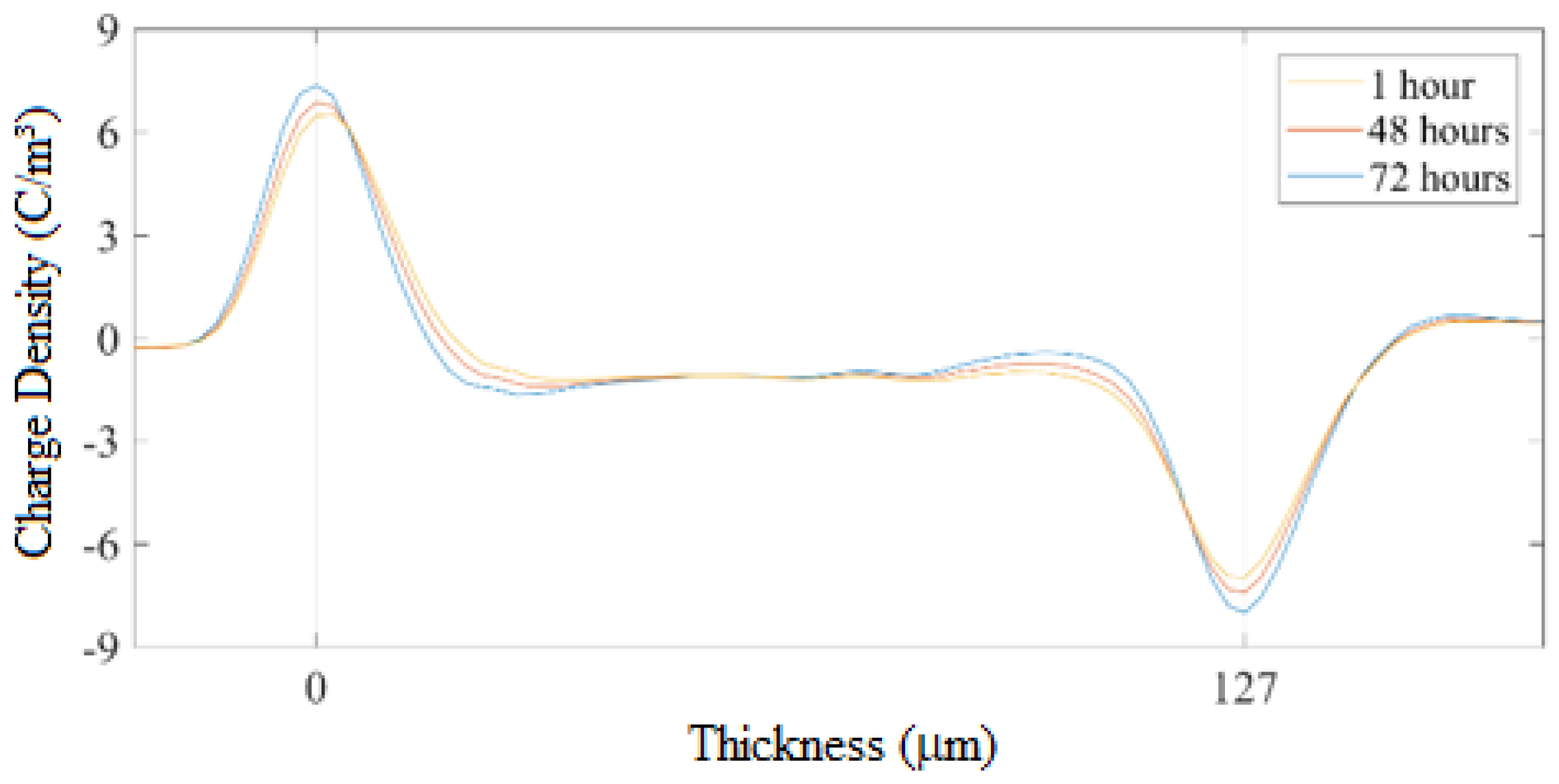
However, in order to have some useful information, the charge distribution was evaluated on a single-layer Kapton specimen with the PEA method [20]. The specimen was subjected to DCP with δ = 0.6 and a magnitude of 7 kV for 72 h. The obtained profiles are reported in Figure 11.
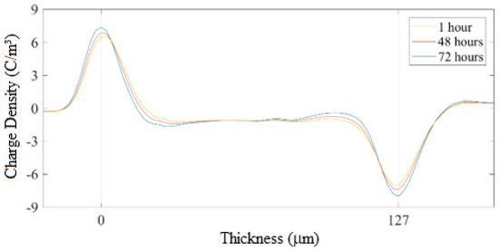
Figure 11.
Space charge profiles in a single layer Kapton specimen under 5 kV DCP with δ = 0.6 after 1, 48 and 72 h.
As can be observed in the charge pattern, the accumulation of the charge is mainly located at the sample faces, whilst, in its bulk, the accumulated charge is very low. This means that, during the experiment, the main part of the accumulated charge is available for the discharge, because it remains proximity to the air–Kapton void surface.
Considering that, in the specimen of Figure 3, the high-voltage electrode is made by stainless steel, the HV electrode/air interface conditions do not change over time, apart a different accumulation of the interfacial charge. In the air/Kapton interface, instead, variations can be observed. This is because of the chemical and physical properties of the Kapton material, during which after a certain time from the voltage application and, thus, after several PD events, surface carbonization and treeing phenomena occurs.
For the reasons above reported, in the pattern of Figure 10, differences between discharge behaviors during the rising (positive PD) and falling times (negative PD) of applied voltage are present. In fact, during the rising time of the DCP, where the electron emissions start from the air/Kapton interface [21], the PD pattern shows only discharges with a high magnitude (the rabbit ear). On the other hand, the body of the rabbit (constituted by discharges with a low magnitude) is almost invisible after 68 h.
During the falling time of applied voltage, instead, the electron emissions start from the HV electrode/air interface [21]. As can be observed, in this case, the PD pattern does not change over time (from 48 to 72 h), because the interfacial conditions remain the same.
By making a comparison among the patterns of Figure 10 with those detected from 0 to 24 h (Figure 8 and Figure 9), differences in the PD behavior occur. From 0 to 72 h, the obtained patterns during the falling time of applied voltage do not change their shape. The only differences consist in the amount of PD events that is related to the stress application time.
With reference to the patterns detected during the rising time, from 0 to 24 h, the shape is almost the same, whilst, after 48 h, a substantial difference was observed for the reasons previously explained.
Further details concerning the explanation of the PD behavior will be given in the Section 5.
4. Detected PD Pulse
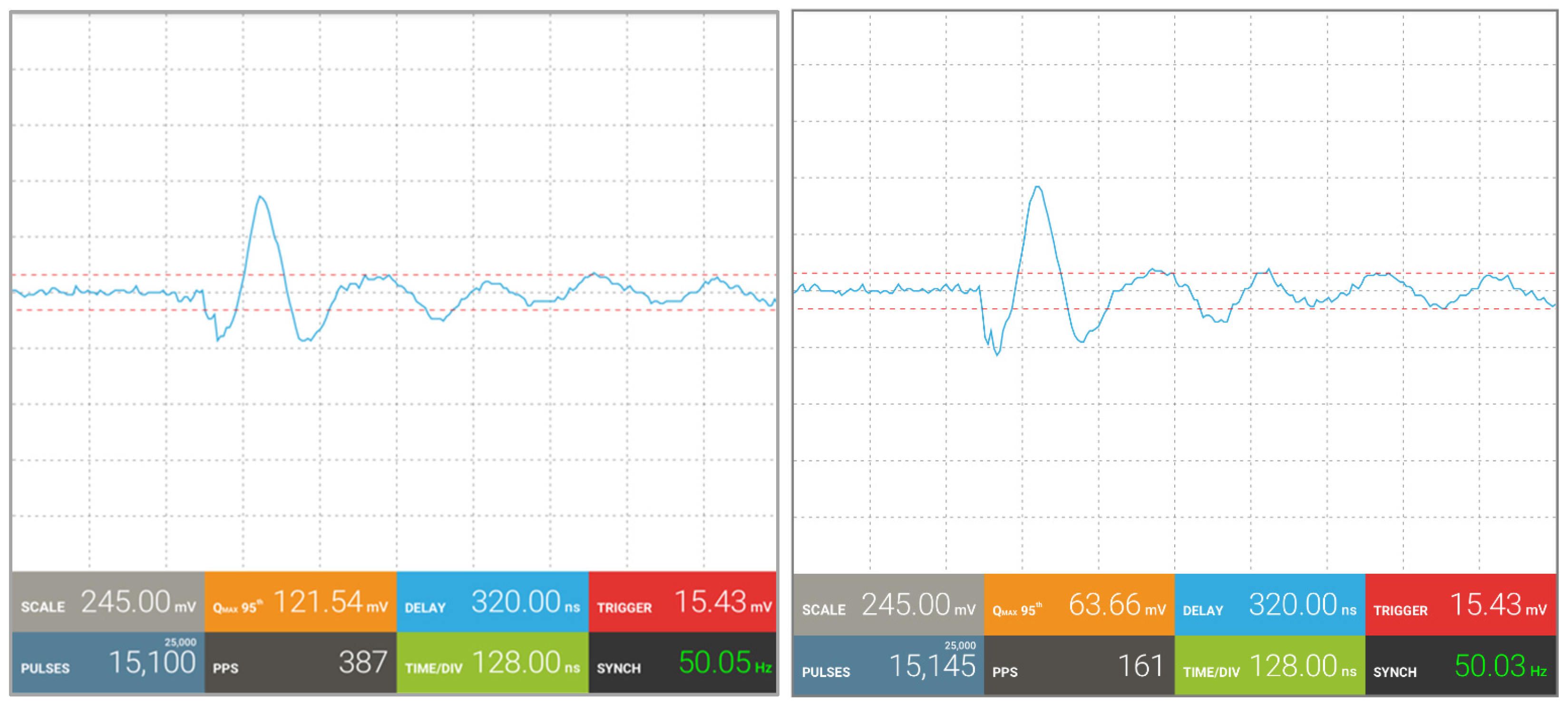
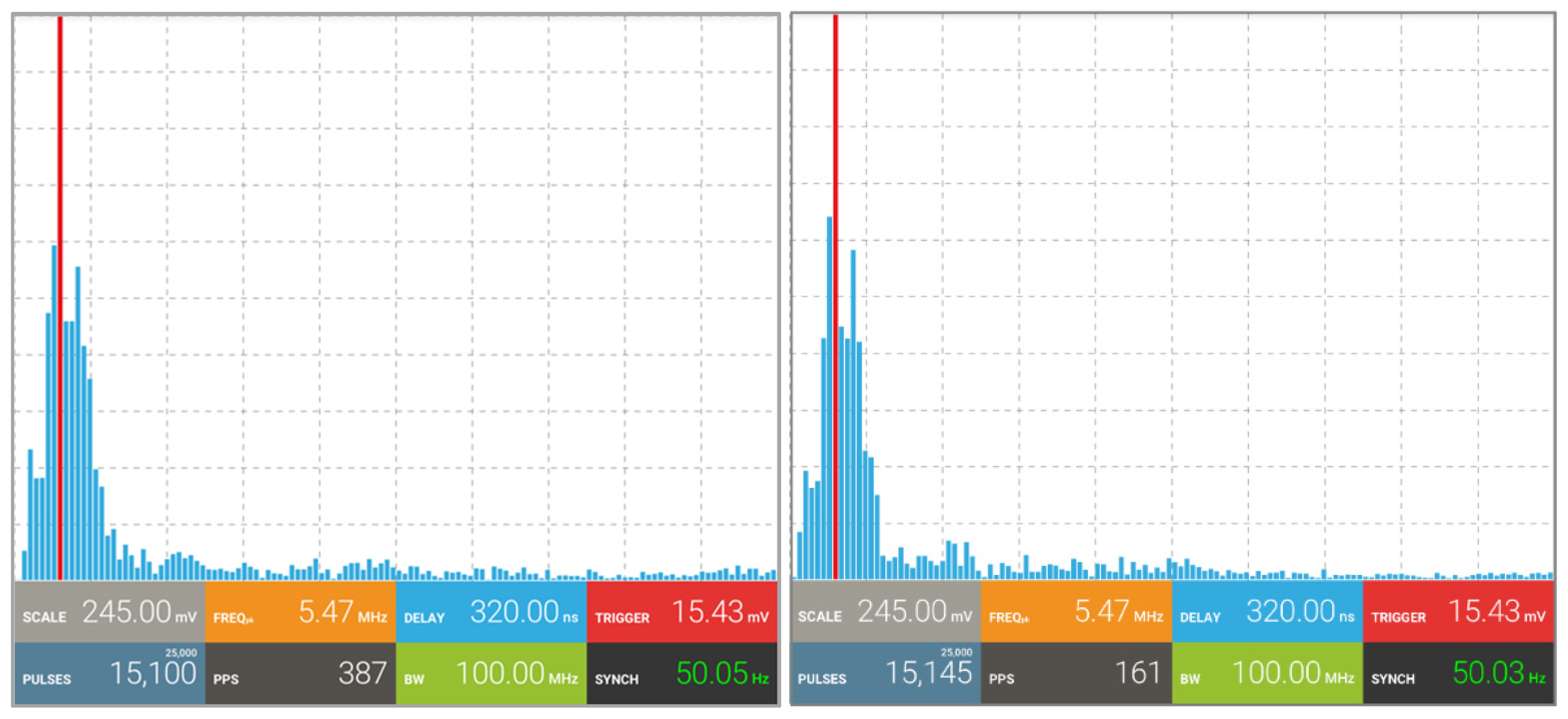
In order to confirm the detection of internal discharges, a comparison between individual PD pulses and their spectra, sensed during the application of both sinusoidal and the DCP waveforms with δ = 0.6, are reported in Figure 12 and Figure 13, respectively. This comparison is useful to confirm that the effect of the DCP waveform on PD behavior and detection, independently of the δ value, is the same of that produced by traditional sinusoidal stress.
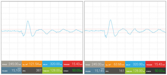
Figure 12.
Typical time domain waveforms of internal time domain PD pulses detected by the Pry-cam sensor with the sinusoidal (left) and the DCP waveforms with δ = 0.6 (right).
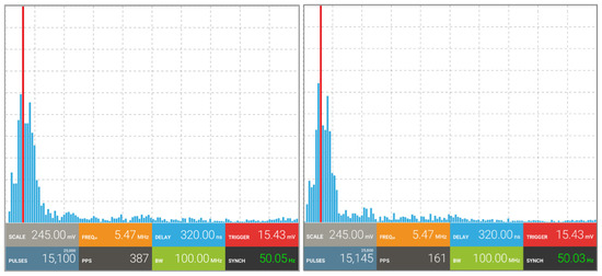
Figure 13.
Typical frequency spectrum related to the PD pulse detected by the Pry-cam sensor with the sinusoidal (left) and the DCP waveforms with δ = 0.6 (right).
5. Discussion
To better clarify the obtained results, a more in-depth analysis is reported in this section.
With regards to the PRPD pattern obtained by means of the DCP with δ = 0, it has been found that its behavior is very similar to that obtained under a conventional sinusoidal waveform. The most evident differences consist of higher pulses per second (PPS) of the patter acquired under AC stress. This is because the AC voltage stress shape promotes the PD events during the entire waveform period. On the other hand, DCP enhances the discharges only during the sinusoidal part of its shape, such as the half-waveform period for the DCP with δ = 0.
The PRPD pattern for the DCP waveform with δ = 0.6, instead, is different from that obtained under AC and DCP with δ = 0. Certainly, the differences are mainly due to the waveform shape, which, in this case, has a smaller sinusoidal part. However, from 0 to 24 h of voltage application, the PRPD patterns have almost the same shape. Nevertheless, due to the asymmetry of the specimen under testing, the PDIV detected during the rising time was different from that at the falling time. This, of course, causes a different positive (during the rising time) and negative (during the falling time) discharge behaviors [22]. Beyond this, a substantial difference between positive and negative discharge behaviors but, also, between the previous described patterns (under AC, DCP with δ = 0 and DCP with δ = 0.6 until 24 h) and the pattern related to the DCP with δ = 0.6 detected from 48 to 72 h, was observed.
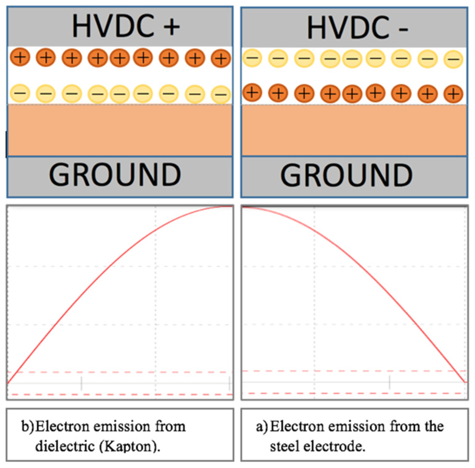
As previously explained, the main cause of PRPD pattern differences can be attributed to the fact that, during the rising time of applied voltage, the electrons are emitted from the air/Kapton interface, while during the falling time, the electron emissions are provided by the opposite void surface, such as the HV electrode/air interface, as depicted in Figure 14.
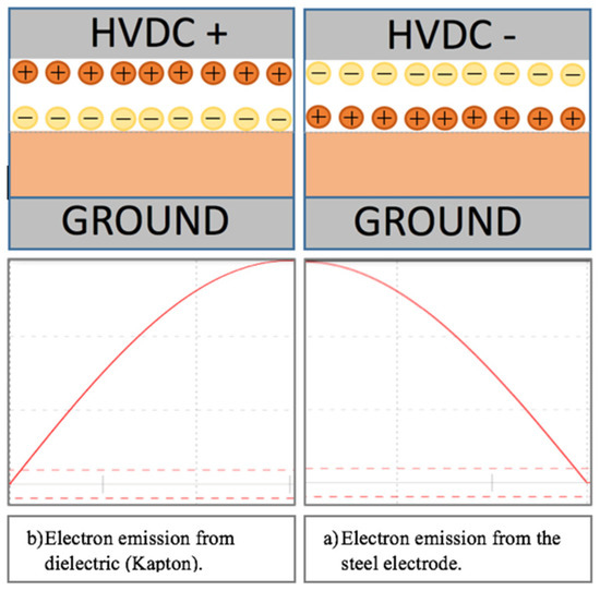
Figure 14.
Specimen representation and charge distribution inside the cavity before positive (a) and negative (b) discharges.
Considering that the HV electrode/air interface conditions do not change during the time (because the steel electrode is not affected by aging phenomena), no particular differences are present in the patterns for the negative discharges. On the contrary, in the air/Kapton interface, the aging phenomena (e.g., for treeing, charge accumulation and cavity erosion phenomena) greatly influences the positive discharge behaviors. In fact, compared to the patterns acquired from 0 to 24 h (see Figure 9), after 48 h of voltage application (see Figure 10), only PD with a high magnitude is present in the detected patterns. Therefore, the transition from the “rabbit-like” pattern to a “wing-like” occurs, as found by T. Tanmaneeprasert and P.L. Lewin in Reference [23] by applying sinusoidal stress for 1004 h in a polyethylene sample. In addition, it was found that this phenomenon can also be attributed to the residual charge deposited after the last negative discharge, which influences the positive PD events of the next DCP cycle.
This last aspect was widely analyzed by Pan C. et al. in Reference [24], where, by means of the chopped PD (CPD) method [25], the residual charge generated during PD events was magnified. In their work, the CPD method was applied in a specimen containing an air void and stressed with sinusoidal voltage. It was found that the enhancement effect generated by the residual charge (deposited by the discharges during the negative half-cycle) in the internal electric field distribution decreased in the next positive half-cycle of the applied AC voltage. This, in turn, generated an increase in the PDIV, as well as in the phase angle of the positive discharges. Moreover, in Reference [24], it also reported that “the reduction of free electron supply may be responsible for the increasing of the maximum PD magnitude”, which was the same effect detected in our experimental test.
6. Conclusions
In this paper, a first evaluation of the time dependence of the partial discharges occurring inside a dielectric by applying the recently developed DCP waveform was carried out with the purpose of confirming the effectiveness of acquiring PRPD patterns under DCP after several hours of voltage application, as well as evaluating the aging effect on the dielectric materials.
The experimental results showed that the obtained PRPD patterns under the DCP waveform followed a similar trend of those obtainable under AC stress. In particular, the classic “rabbit-like” pattern, which provided internal discharge information under AC, was also detected for the DCP with δ = 0. The main differences among the AC and DCP patterns were essentially due to the DCP shape, which contained a constant part able to emphasize the space charge accumulation phenomenon, as under DC stress. On the contrary, with reference to the results obtained with the DCP having δ = 0.6, instead, the transition to a “wing-like” pattern, where only a high-magnitude PD was observed, was validated by means of comparison with other PD patterns found in the literature.
On the basis of the obtained results, it was possible to confirm that the proposed DCP waveform and, in particular, that with δ = 0.6, which allowed a charge accumulation similar to that occurring under DC stress, provided PRPD patterns easily interpretable. This was because their shape was similar to the widely known pattern obtainable under the AC stress.
In order to emphasize the aging effect, future developments of this work will be focused on the same types of measurements procedures but in dielectric materials able to accumulate a higher amount of space charge in less time, such as XLPE.
In conclusion, for testing HVDC cable systems, the effect on PD evolution due to phenomena such as space charge diffusion, the presence of a thermal gradient and other phenomena occurring under DC cannot be neglected. These phenomena affect the electric field distribution inside the dielectric and, even more so, in the presence of defects such as air cavities, showing an evolution of the aging mechanisms very different from that occurring under AC voltage. The proposed method has the benefit of considering these phenomena and the downside of needing an additional device, described in depth in a previous paper, whose cost will be proportional to the voltage level to be reached.
Author Contributions
Conceptualization, methodology and investigation, A.I.; software and calculations, A.I. and G.R.; validation, P.R. and G.A. writing—original draft preparation, A.I. and writing—review and editing, A.I., G.R., P.R., G.A. and R.C. All authors have read and agreed to the published version of the manuscript.
Funding
This research received no external funding.
Data Availability Statement
Not applicable.
Conflicts of Interest
The authors declare no conflict of interest.
References
- Morshuis, P.; Cavallini, A.; Fabiani, D.; Montanari, G.C.; Azcarraga, C. Stress conditions in HVDC equipment and routes to in service failure. IEEE Trans. Dielectr. Electr. Insul. 2015, 22, 81–91. [Google Scholar] [CrossRef]
- Gulski, E.; Krivda, A. Neural networks as a tool for recognition of partial discharges. IEEE Trans. Dielectr. Electr. Insul. 1993, 28, 984–1001. [Google Scholar] [CrossRef] [Green Version]
- Candela, R.; Mirelli, G.; Schifani, R. PD recognition by means of statistical and fractal parameters and a neural network. IEEE Trans. Dielectr. Electr. Insul. 2000, 7, 87–94. [Google Scholar]
- Peng, X.; Yang, F.; Wang, G.; Wu, Y.; Li, L.; Li, Z.; Bhatti, A.A.; Zhou, C.; Hepburn, D.M.; Reid, A.J. A Convolutional Neural Network-Based Deep Learning Methodology for Recognition of Partial Discharge Patterns from High-Voltage Cables. IEEE Trans. Power Deliv. 2019, 34, 1460–1469. [Google Scholar] [CrossRef]
- CIGRÉ Technical Brochure 496; Recommendations for Testing DC Extruded Cable Systems for Power Transmission at a Rated Voltage up to 500 kV. 2012. Available online: https://e-cigre.org/publication/496-recommendations-for-testing-dc-extruded-cable-systems-for-power-transmission-at-a-rated-voltage-up-to-500-kv-this-tb-replaces-tb-219 (accessed on 15 February 2022).
- IEC Standard 62895; High Voltage Direct Current (HVDC) Power Transmission Cables with Extruded Insulation and Their Accessories for Rated Voltages up to 320 kV for Land Applications-Test Methods and Requirement. 2017. Available online: https://webstore.iec.ch/publication/34020 (accessed on 15 February 2022).
- Mazzanti, G.; Castellon, J.; Chen, G.; Fothergill, J.C.; Fu, M.; Hozumi, N.; Lee, J.H.; Li, J.; Marzinotto, M.; Mauseth, F. The insulation of HVDC extruded cable system joints. Part 1: Review of materials, design and testing procedures. IEEE Trans. Dielectr. Electr. Insul. 2019, 26, 964–972. [Google Scholar] [CrossRef]
- Mazzanti, G.; Castellon, J.; Chen, G.; Fothergill, J.C.; Fu, M.; Hozumi, N.; Lee, J.H.; Li, J.; Marzinotto, M.; Mauseth, F. The insulation of HVDC extruded cable system joints. Part 2: Proposal of a new AC voltage PD measurement protocol for quality control during routine tests. IEEE Trans. Dielectr. Electr. Insul. 2019, 26, 973–980. [Google Scholar] [CrossRef]
- Morshuis, P.H.; Smit, J.J. Partial discharges at DC voltage: Their mechanism, detection and analysis. IEEE Trans. Dielectr. Electr. Insul. 2005, 12, 328–340. [Google Scholar] [CrossRef] [Green Version]
- Romano, P.; Presti, G.; Imburgia, A.; Candela, R. A new approach to partial discharge detection under DC voltage. IEEE Electr. Insul. Mag. 2018, 34, 32–41. [Google Scholar] [CrossRef]
- Romano, P.; Rizzo, G.; Consolazione, C.; Candela, R.; Ala, G. The Partial Discharge Behavior of Different Materials under DC Periodic Stress. In Proceedings of the IEEE Conference on Electrical Insulation and Dielectric Phenomena (CEIDP), Richland, WA, USA, 20–23 October 2019; pp. 661–665. [Google Scholar]
- Romano, P.; Imburgia, A.; Rizzo, G.; Ala, G.; Candela, R. A New Approach to Partial Discharge Detection under DC Voltage: Application to Different Materials. IEEE Electr. Insul. Mag. 2021, 37, 18–32. [Google Scholar] [CrossRef]
- Imburgia, A.; Romano, P.; Rizzo, G.; Viola, F.; Ala, G.; Chen, G. Reliability of PEA Measurement in Presence of an Air Void Defect. Energies 2020, 13, 5652. [Google Scholar] [CrossRef]
- Romano, P.; Imburgia, A.; Candela, R. Space Charge Measurement under DC and DC Periodic Waveform. In Proceedings of the IEEE Conference on Electrical Insulation and Dielectric Phenomena (CEIDP), Cancun, Mexico, 21–24 October 2018; pp. 293–296. [Google Scholar]
- Candela, R.; Di Stefano, A.; Fiscelli, G.; Giaconia, G.C. Portable Partial Discharge Detection Device. Patent EP2297589/WO2009150627, 11 June 2009. [Google Scholar]
- Romano, P.; Imburgia, A.; Ala, G. Partial Discharge Detection Using a Spherical Electromagnetic Sensor. Sensors 2019, 19, 1014. [Google Scholar] [CrossRef] [PubMed] [Green Version]
- Tanmaneeprasert, T.; Lewin, P.L. The use of partial discharge analysis for the diagnosis of electrical ageing in polymeric insulation containing cavities. In Proceedings of the IEEE Electrical Insulation Conference (EIC), Montreal, QC, Canada, 19–22 June 2016; pp. 383–387. [Google Scholar]
- Tanmaneeprasert, T.; Lewin, P.L.; Hunter, J.A. Influence of internal discharges in a cavity within polymeric insulating material caused by partial discharge mechanisms. In Proceedings of the IEEE Conference on Electrical Insulation and Dielectric Phenomena (CEIDP), Ann Arbor, MI, USA, 18–21 October 2015. [Google Scholar]
- Wang, L.; Cavallini, A.; Montanari, G.C.; Testa, L.; Spa, T. Patterns of partial discharge activity in XLPE: From inception to breakdown. In Proceedings of the 10th IEEE International Conference on Solid Dielectrics, Potsdam, Germany, 4–9 July 2010; pp. 1–4. [Google Scholar]
- Imburgia, A.; Miceli, R.; Sanseverino, E.R.; Romano, P.; Viola, F. Review of space charge measurement systems: Acoustic, thermal and optical methods. IEEE Trans. Dielectr. Electr. Insul. 2016, 23, 3126–3142. [Google Scholar] [CrossRef]
- Montanari, G.C. Bringing an insulation to failure: The role of space charge. IEEE Trans. Dielectr. Electr. Insul. 2011, 18, 339–364. [Google Scholar] [CrossRef]
- Cavallini, A.; Conti, M.; Montanari, G.C.; Contin, A.; Candela, R.; Romano, P.; Schifani, R. Searching for PD-based indexes able to infer the location of internal defects in insulation. In Proceedings of the IEEE Conference on Electrical Insulation and Dielectric Phenomena (CEIDP), Cancun, Mexico, 20–24 October 2002; pp. 703–706. [Google Scholar]
- Tanmaneeprasert, T.; Lewin, P.L. Electrical treeing and ageing characteristics in cavities of low density polyethylene dielectrics on partial discharge measurements. In Proceedings of the IEEE Conference on Electrical Insulation and Dielectric Phenomena (CEIDP), Toronto, ON, Canada, 16–19 October 2016; pp. 975–978. [Google Scholar]
- Pan, C.; Wu, K.; Chen, G.; Gao, Y.; Florkowski, M.; Lv, Z.; Tang, J. Understanding Partial Discharge Behavior from the Memory Effect Induced by Residual Charges: A Review. IEEE Trans. Dielectr. Electr. Insul. 2020, 27, 1951–1965. [Google Scholar] [CrossRef]
- Florkowski, M.; Florkowska, B.; Zydron, P. Chopped partial discharge sequence. IEEE Trans. Dielectr. Electr. Insul. 2015, 22, 3451–3458. [Google Scholar] [CrossRef]

Publisher’s Note: MDPI stays neutral with regard to jurisdictional claims in published maps and institutional affiliations. |
© 2022 by the authors. Licensee MDPI, Basel, Switzerland. This article is an open access article distributed under the terms and conditions of the Creative Commons Attribution (CC BY) license (https://creativecommons.org/licenses/by/4.0/).