Article

Analysis and Design of the Split-Capacitor-Based Sub-Modules Equipped for Hybrid Modular Multilevel Converter

1
Department of Electrical Engineering, School of Automation, Northwestern Polytechnical University, Xi’an 710054, China
2
State Grid Xian Electric Power Supply Company, Xi’an 710032, China
*
Author to whom correspondence should be addressed.
Energies 2022, 15(7), 2370; https://doi.org/10.3390/en15072370
Submission received: 24 February 2022 / Revised: 17 March 2022 / Accepted: 22 March 2022 / Published: 24 March 2022

Abstract

:
The hybrid modular multilevel converter (MMC) is always featured and profited by the merits of the equipped power valves. Referring to this, a novel hybrid MMC topology equipped with the split-capacitor-based sub-modules (SCSMs) on the AC side is proposed. It aims to increase the utilization of the DC bus voltage with DC fault blocking capability. Especially compared to the hybrid MMC equipped with the full-bridge-based sub-modules (FBSMs) on the AC side, smaller power losses can be achieved for the proposed hybrid MMC, due to the reason that only one semiconductor device of the SCSM is inserted into the current flow route. Structurally, the proposed converter mainly consists of the half-bridge-based sub-module (HBSM) stacks and SCSM stacks. The HBSMs located on the DC converter side of the proposed hybrid MMC are in charge of exchanging active powers, while the SCSMs located on the AC converter side are in charge of shaping the circuit waveforms. Additionally, profited by the specific structure of the SCSM, the DC fault current could be cut off by imposing inversed voltages collected from the SCSM capacitor voltages on the uncontrollable diodes of the IGBTs. For the deep study, a detailed mathematical model and modulation control of the proposed hybrid MMC are analyzed. In addition, an analysis of the balancing control for SCSMs is also provided. Finally, the simulation and experimental results are proposed to verify the effectiveness of the theoretical analysis.

1. Introduction

The modular multilevel converter (MMC) is supposed to be one of the most competitive topologies for medium to high voltage applications due to its modular nature, low power loss, small voltage step, and redundancy nature [1,2,3,4,5,6,7]. Unlike the two-level voltage source converter (VSC) equipped with the bucky capacitor to support the DC bus voltage, the optimized scheme from the MMC system proposes to split the high voltage capacitor in the VSC to substitute with distributed capacitors, which improves the reliability of the MMC system. For years of development of the MMC investigation, attention has been mostly focused on the circulating current suppressing control (CCSC), balancing control, power quality improvement, etc. [8,9,10,11,12,13,14,15,16]. These features make MMC topology a promising scheme for medium to high voltage applications.
For long-distance power transmissions, the high-voltage-direct-current (HVDC) system has shown a promising prospect for its higher efficiency and lower cost as compared to the high-voltage-alternating-current (HVAC) system. Typically, due to the cost-effective and maintainability features, the overhead line is supposed to be a feasible way for HVDC transmission. However, considering the condition that the overhead line is vulnerable to external environmental factors, different kinds of DC faults frequently occur for the overhead line HVDC system. Although the DC breaker may be an alternative scheme for blocking the DC fault current, it introduces unneglected, on-state power losses and is limited by the immature technology and expensive cost. Typically, for HBSM-based MMC systems, the uncontrollable antiparallel diodes of the IGBTs are the key factor for providing the fault current flow route when the DC fault occurs [17]. Thus, a considered approach recommends adopting the MMC station with enabled DC fault blocking capability [18]. Technically, it would be a preferred solution by imposing inverse voltages on these uncontrollable diodes of the IGBTs, which is mainly achieved by the full-bridge sub-module (FBSM)-based MMC (FBSM-MMC) [19]. However, a large number of the FBSMs in the FBSM-MMC accompany high cost and serious power loss.
Considering the above-mentioned problems, the concept of the hybrid MMC system is introduced. These MMC topologies consist of different types of power valves, which integrate the merits of the equipped power valves. Presently, a hybrid MMC consisting of the direct switchers (DSs) and the FBSM stacks is presented in [20], which is named the hybrid cascaded multilevel converter (HCMC). In normal operation, the FBSM stacks in HCMC are in charge of shaping the output voltage, while the DSs aim to control the active power transmission. Especially, the DSs in HCMC can be operated at the fundamental frequency, significantly reducing power losses. However, the HCMC is restricted to limited applications for its weak dynamic and static characteristics when a large number of IGBTs in DSs are cascaded. Therefore, the alternative combination recommends integrating the merits of the HBSMs and FBSMs. Recently, various kinds of these hybrid MMC topologies have been investigated. A hybrid MMC topology equipped with the HBSMs and FBSMs for each arm is studied in [21]. The theoretical analysis concluded that once the number of HBSMs and FBSMs is designed properly, the DC fault blocking capability can be enabled. Compared to the FBSM-MMC, the hybrid MMC in [21] could save the semiconductor devices and power losses partly. However, the distribution of the SM voltage references between the HBSMs and FBSMs complicates the control system. To relieve this problem, another alternative hybrid topology with cascade FBSMs on the AC side, as illustrated in Figure 1, is presented in [22]. By diverting the cascaded FBSMs from the converter arm to AC side, the control of the HBSMs and FBSMs of the hybrid MMC in [22] could be divided separately, which extremely simplified the control structure. Additionally, in the point of balancing the FBSM capacitor voltages, since no fundamental frequency component is involved in the FBSM voltage reference, the FBSM capacitor voltages can be easily balanced. Meanwhile, since the FBSM stacks are in charge of filtering the harmonics, smaller FBSM capacitance can be designed. Furthermore, compared to the FBSM stacks used to transfer the active powers in [21], the evenly distributed power losses of the FBSMs in [22] can be achieved, providing better reliability in terms of the power switches. However, due to there being two semiconductor devices of the FBSM inserted in the current flow route, the serious power losses of the hybrid MMC restricts its development.
Of all the above-mentioned problems, this paper proposes a novel hybrid MMC equipped with the novel split-capacitor-based sub-modules (SCSMs) on the AC side. Structurally, the proposed converter mainly consists of the cascaded HBSM and SCSM stacks. The HBSM stacks in the proposed hybrid MMC are in charge of exchanging the active powers, while the SCSM stacks acting as the wave shaping circuit are responsible for filtering the output voltages. Compared to the hybrid MMC with FBSMs on the AC side in Figure 1, and due to the reason that there is only one semiconductor device of the single SCSM in the SCSM current flow route, the proposed topology can be enabled with the enlarged AC output voltage and the DC fault blocking capability with smaller losses and switch devices. Additionally, to further explore the performance of the proposed hybrid MMC, the mathematic model, control strategy, and the SCSM design are also provided. Finally, the simulation and experimental results are implemented to verify the effectiveness of the theoretical analysis.
This paper is organized as follows. Section 2 gives the detailed analysis and mathematical model of the proposed hybrid MMC. In Section 3, the modulation principle of the proposed hybrid MMC is discussed, and the corresponding control strategy is also provided. To verify the effectiveness of the proposed topology and theoretical analysis, the simulation and experimental results are achieved in Section 4 and Section 5, respectively. Finally, Section 6 concludes the entire work.

2. Analysis of the Proposed Hybrid MMC Topology

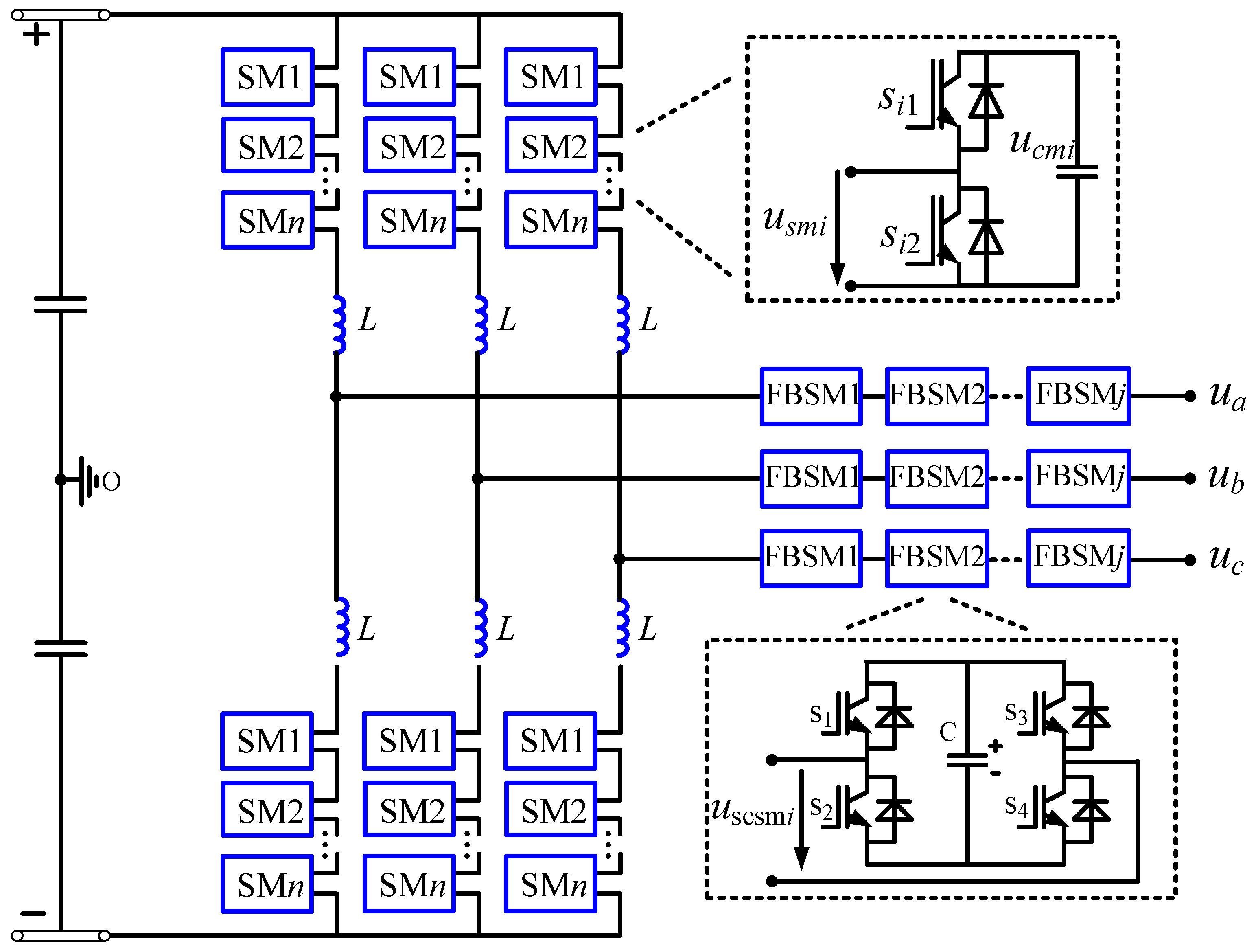
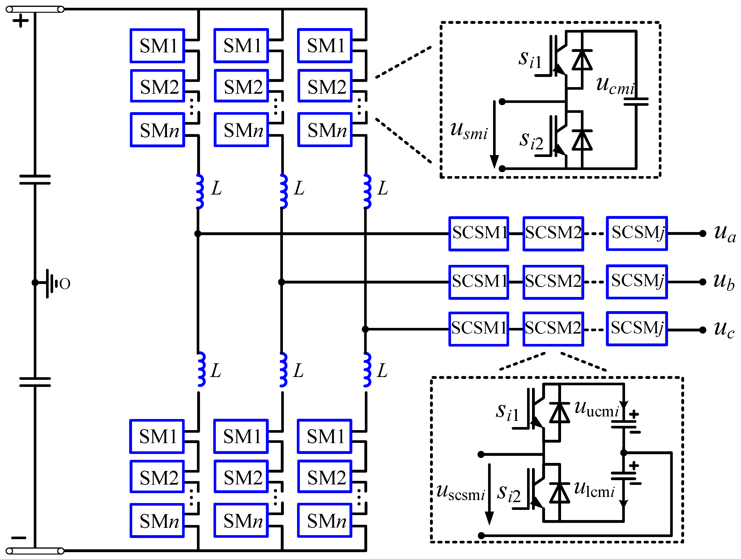
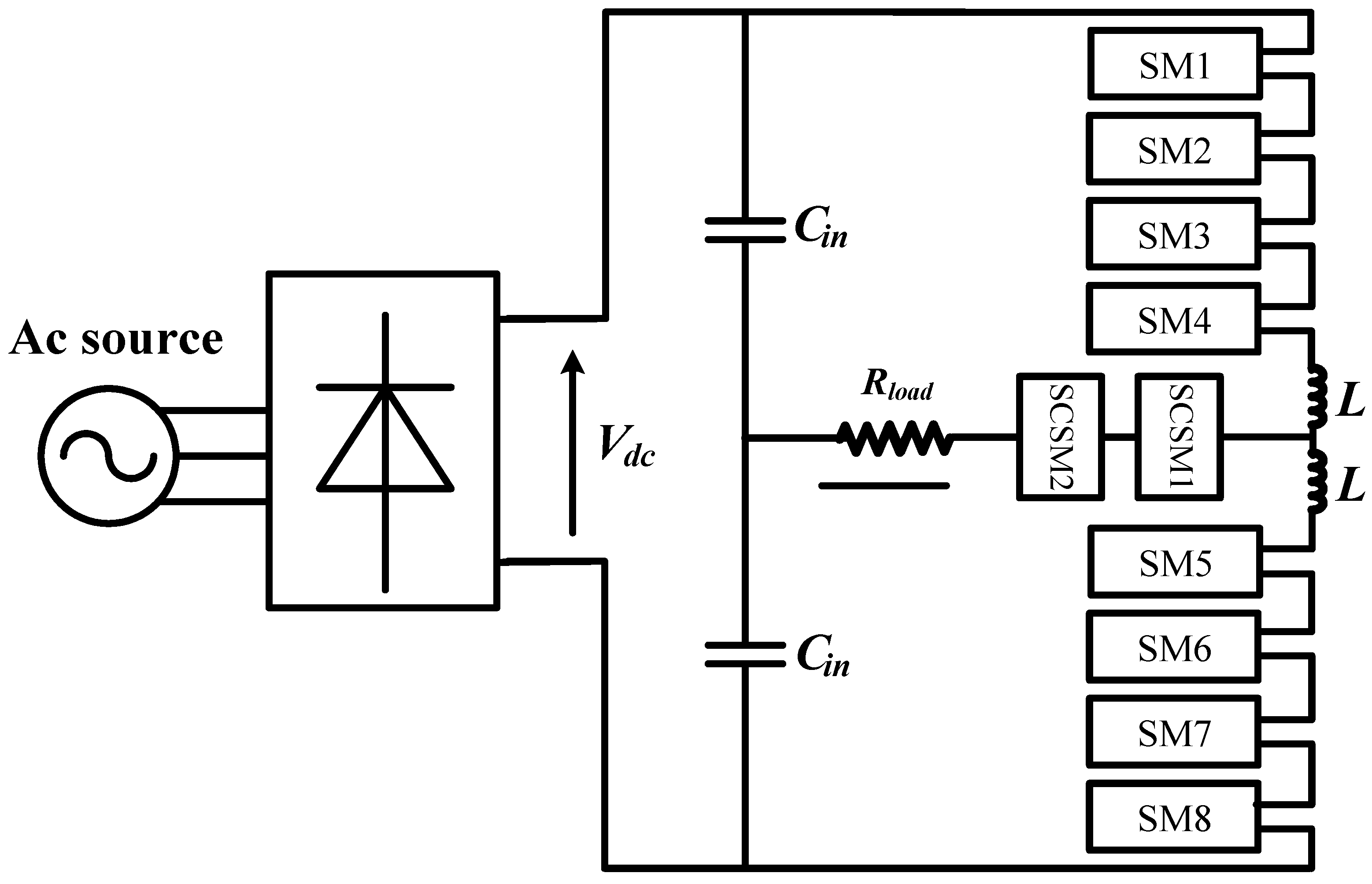
2.1. Basic Structure of the Proposed Hybrid MMC

The schematic of the proposed hybrid MMC topology is illustrated in Figure 2. It consists of the power stage and the wave shaping stage. As illustrated in Figure 3a, the power stage of the proposed hybrid MMC, consisting of the HBSM stacks and the arm reactors, is mainly in charge of exchanging the active powers. The wave shaping stage, consisting of the SCSM stacks, is mainly in charge of filtering the undesired harmonics. Structurally, it observes that the SCSM is evolved from the HBSM by splitting the HBSM capacitor for pulling the negative output terminal of the SCSM. The specific structure of the SCSM topology reflects the entirely different SM characteristics, providing additional functionality for the proposed hybrid MMC.
As the illustration of the SCSM structure in Figure 3b shows, it consists of two insulated gate bipolar transistors (IGBTs) and two split capacitors. Based on the circuit characteristics of the SCSMs, two working operations can be collected as listed in Table 1: the normal operation mode, and the fault blocking operation mode. In normal operation, the IGBTs of the SCSM are driven with complementary signals. As shown in Table 1, when si1 is on and si2 is off, the SCSM outputs the upper split capacitor voltage uucmi. When si1 is off and si2 is on, the SCSM outputs the lower split capacitor voltage ulcmi. Thus, the required SCSM voltages can be obtained by chopping the split capacitor voltages. Specifically, the positive and negative voltage levels of the SCSM voltage are derived from the upper and lower SCSM capacitor voltages, respectively.
Typically, compared to the hybrid MMC equipped with FBSM stacks on the AC side (shown in Figure 1), the proposed hybrid MMC has smaller power losses and power devices due to the equipped SCSM stacks. To illustrate this feature, the current flow routes of the FBSM and SCSM under the basic operation principle are depicted in Figure 4 and Figure 5, respectively. In Figure 4, it shows that there are always two power switches involved in the FBSM current flow route, and either the IGBT or its antiparallel diode working in the FBSM current route is decided by the current direction. Unlike the FBSM, as shown in Figure 5, there is only one power switch involved in the SCSM current flow route, significantly reducing the power losses. Furthermore, due to the split-capacitor feature of the SCSM, the fault current route can be safely cut off by properly designing the SCSM number, enabling the DC fault blocking capability of the proposed hybrid MMC.
Therefore, with the discussion of the specific feature for SCSM, the basic control principle of the proposed hybrid MMC is introduced, which integrates the merits of the HBSMs and SCSMs. The HBSM stacks of the proposed hybrid MMC were used to control the active power transmission and produce the required multilevel phase voltage. Normally, the HBSM arms contain the sinusoidal load voltage (vx) and the modified harmonic pat (vh). The modified harmonic part (vh), utilized to redesign the shape of the arm voltage reference, aimed to achieve the enlarged AC output voltage by avoiding the overmodulation process. Thus, the enlarged utilization of the DC bus voltage in the proposed hybrid MMC can proceed. As for the output voltage distorted by the modified harmonic parts, it was removed by controlling the SCSM stacks to produce an inverse vh. In this condition, the SCSM stacks served as the active filters (APF) in the proposed hybrid MMC.

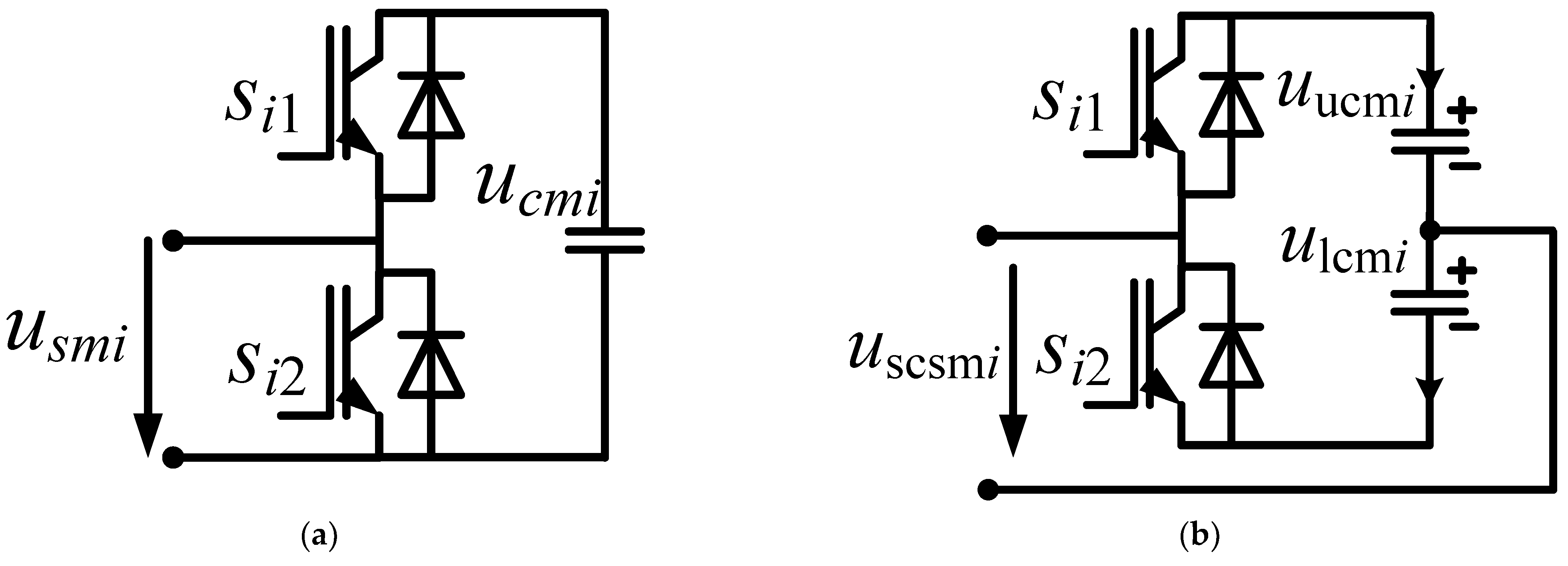
2.2. Model and Analysis of the Proposed SCSM

Considering the discussion above, the terminal voltage of the SCSM can be expressed as
u s c s m i = s i 1 u u c m i s i 2 u l c m i , i = 1 , 2 ,     ,   j
where uxucmi and uxlcmi are the upper and lower split capacitor voltages of the i-th SCSM in phase x (x = a, b, c), respectively, and sxyi (x = a, b, c; y = 1, 2; i = 1, 2, …, j) denotes the i-th SCSM switching function. For simplification, the switching function of the SCSM is defined as
s x y i = { 1 ,   when   switch   is   on 0 ,   when   switch   is   off i = 1 , 2 , ,   j
From Equations (1) and (2), they show that the SCSM voltage usscsm under a specified instant is only contributed by one of the SCSM capacitor voltages. Therefore, the output voltages of the SCSM stacks can be expressed as
u x s c s m = i = 1 j u x s c s m i = i = 1 j ( s x i 1 u x u c m i s x i 2 u x l c m i )
where uxscsm is the output voltage of the SCSM stack in phase x (x = a, b, c). It is assumed that the SCSM stacks are operated at sufficient high switching frequency and the upper and lower SCSM capacitor voltage references can be treated equally, respectively. Thus, based on Equation (3), the SCSM stack voltage can be modified as
u x s c s m = u x u c m ( i = 1 j s x i 1 ) u x l c m ( i = 1 j s x i 2 )
where uxucm and uxlcm are the upper and lower SCSM capacitor voltages, respectively. Once a large number of the SCSMs are equipped in the proposed hybrid MMC, the switching functions of the SCSM stack voltage in Equation (4) have a continuous feature. Thus, a different form of Equation (4) can be described as
u x s c s m = j + u x s c r e f 2 u x u c m j u x s c r e f 2 u x l c m
where uxscref is the voltage reference of the SCSM. From Equation (5), it shows that the SCSM stack voltage uxscsm is equal to the SCSM stack voltage reference uxscref once the upper and lower SCSM capacitor voltages are set to be the reference Uref. However, due to the reason that the different capacitor currents exist between the upper and lower SCSM capacitors, the different capacitor voltage ripples appear in the upper and lower SCSM capacitors. This introduces an inverse ripple shape of the upper and lower SCSM capacitor voltages.

2.3. Model and Analysis of the Proposed Hybrid MMC

The proposed hybrid MMC integrated both the merits of the HBSM and SCSM stacks. The HBSM stacks served as the power stage of the proposed hybrid MMC, while the SCSM stacks served as the filter stage. In normal operation, the SCSM stacks can be treated as the harmonic voltage generator (HVG), producing any required harmonic voltages for rearranging the power distribution. This supplies an additional degree of freedom for improving the performance of the proposed hybrid MMC. To investigate the system feature, it was necessary to build the mathematic model of the proposed hybrid MMC, which is
{ 1 2 V d c u x u L d i x u d t u x s c s m = u x 1 2 V d c + u x l + L d i x l d t u x s c s m = u x
where uxu and uxl are the upper and lower arm voltages of phase x (x = a, b, c) in the proposed hybrid MMC, respectively, ixu and ixl are the upper and lower arm currents of phase x (x = a, b, c) in the proposed hybrid MMC, Vdc is the DC bus voltage, L is the arm inductance, and vx is the output voltage of phase x (x = a, b, c). The mathematic model in Equation (6) is different from that of the traditional MMC, which contains a compensation part uxscsm as the additional degree of freedom for improving the performance of the proposed hybrid MMC. For deep analysis, the DC and AC equivalent models of the proposed hybrid MMC were investigated as
{ V d c u x u u x l 2 L d i x c i r d t = 0 u x l u x u 2 u s c s m L 2 d i x d t = u x
where ixcir and ix are the circulating current and output current of phase x (x = a, b, c), respectively, which are defined as
{ i x c i r = i x u + i x l 2 i x = i x u i x l
In Equation (7), the first equation denotes the DC equivalent model of the proposed hybrid MMC, while the second one denotes the AC equivalent model. It shows that the DC equivalent model in Equation (7) contains no compensation part contributed by the SCSM stacks, which demonstrates an equal feature with that of the traditional MMC topology. The compensated parts from the SCSM stacks mainly influence the characteristic of the AC equivalent model in Equation (7). Figure 6 shows the AC equivalent circuit of the proposed hybrid MMC of a single phase. It shows that the internal electromotive force (IEF) ex, composed of the upper and lower arm voltages, has influences on both the SCSM stack voltage uxscsm and output voltage vx. The IEF shows a strong relation with the distributions of the output voltages, currents, and powers. Therefore, to design the required system feature by modifying IEF, a feasible scheme is to insert corresponding harmonics in uxl and uxu. However, in order to prevent the injected harmonics from changing the DC equivalent model, the corresponding harmonics of the upper and lower arm should have the same amplitude with opposite signs. Figure 7 depicts the equivalent circuit structure of a single-phase. As illustrated, both of the upper and lower arm voltages consisted of the DC parts, fundamental frequency references, and the injected harmonics, which can be expressed as
{ u x u = V d c 2 v x v h u x l = V d c 2 + v x + v h
From Equation (9), the design of the harmonic part vh shows great significance for influencing the system features. The main purpose of this paper prefers to enlarge the realization of the DC bus voltage by introducing the trapezoidal modulation with a proper design of vh, which will be discussed in detail in Section 3. As for the injected harmonics introduced on the AC side, they were eliminated by producing the corresponding compensation parts with the SCSM stacks, which complies with
u s c s m = v h

3. Control and Analysis of the Proposed Hybrid MMC

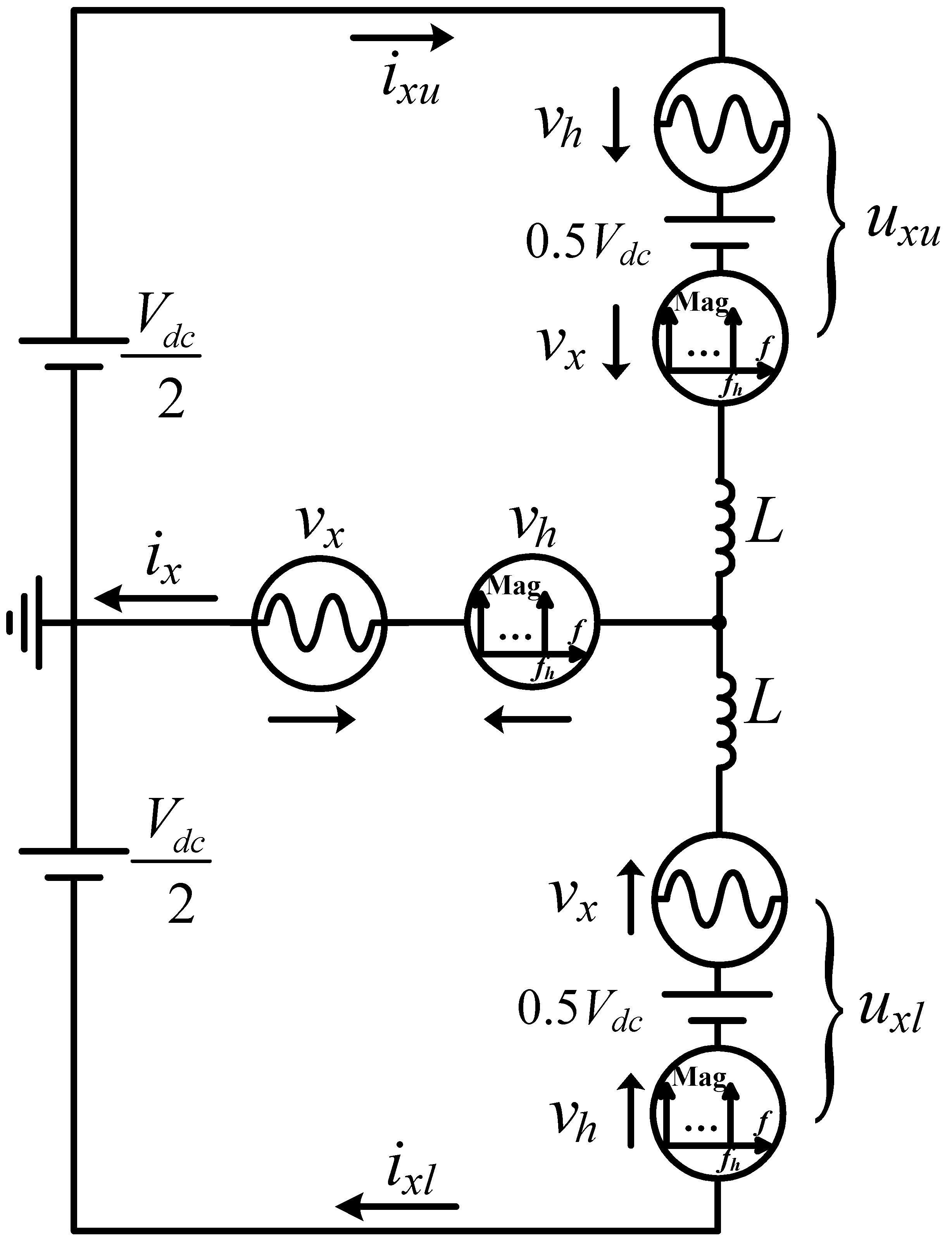
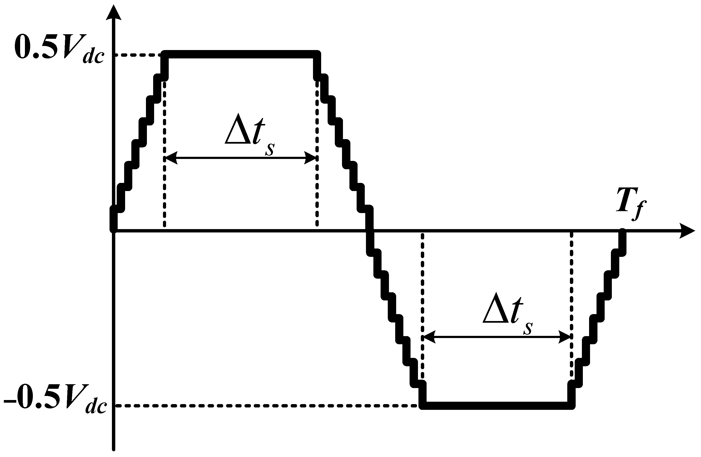
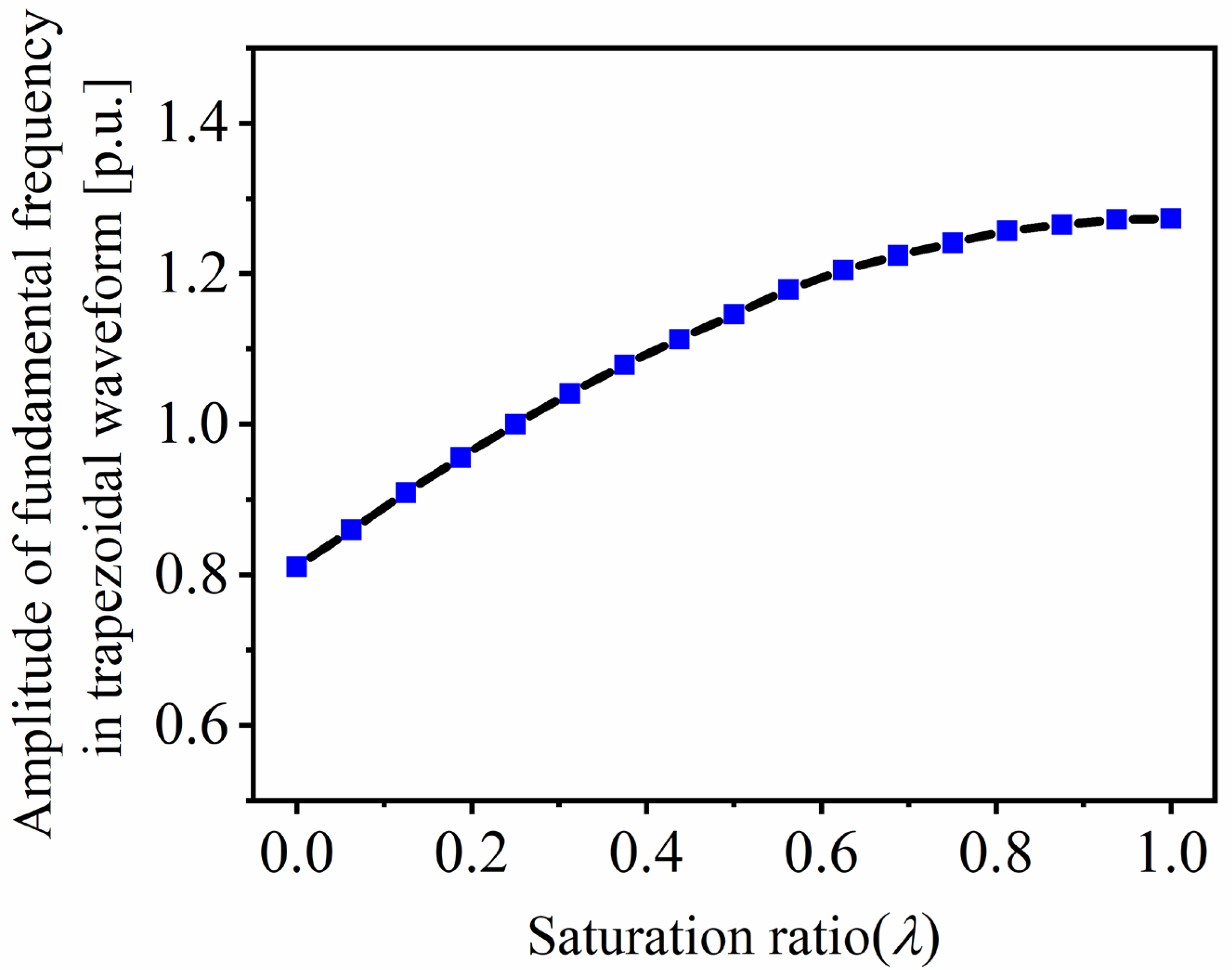
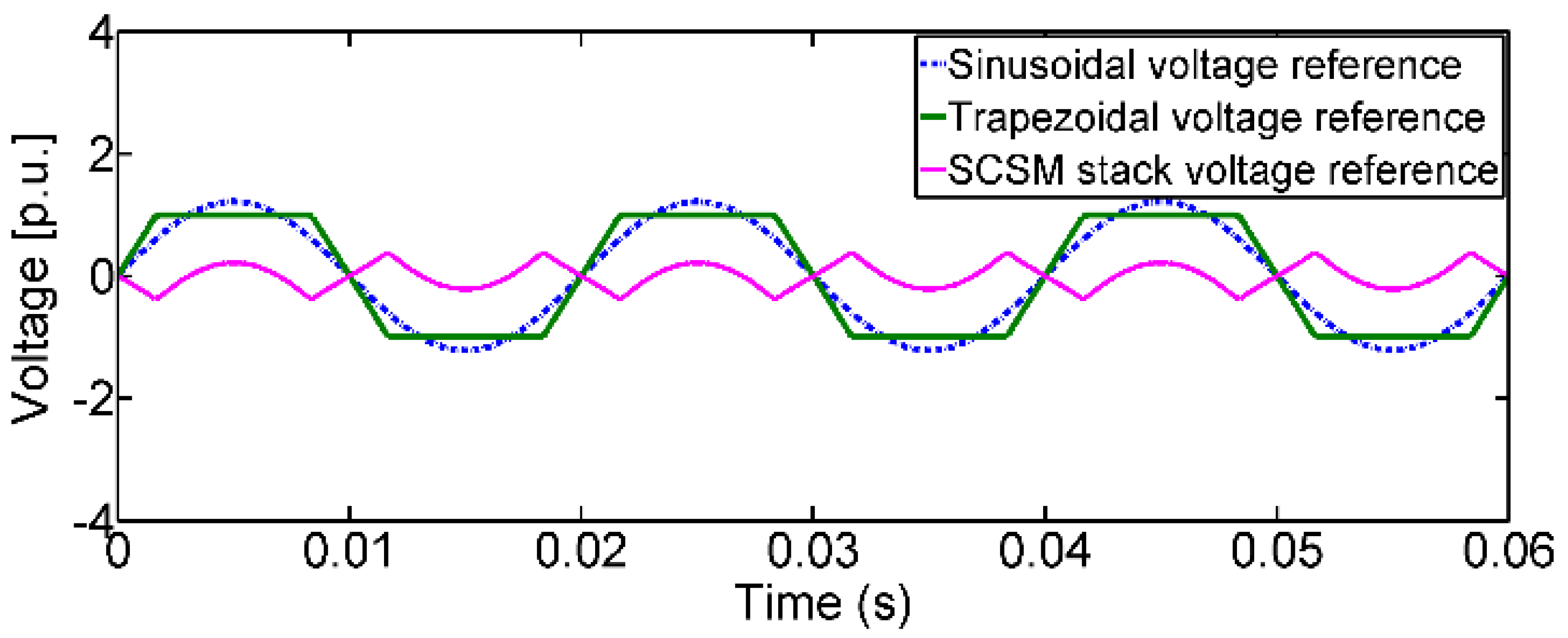
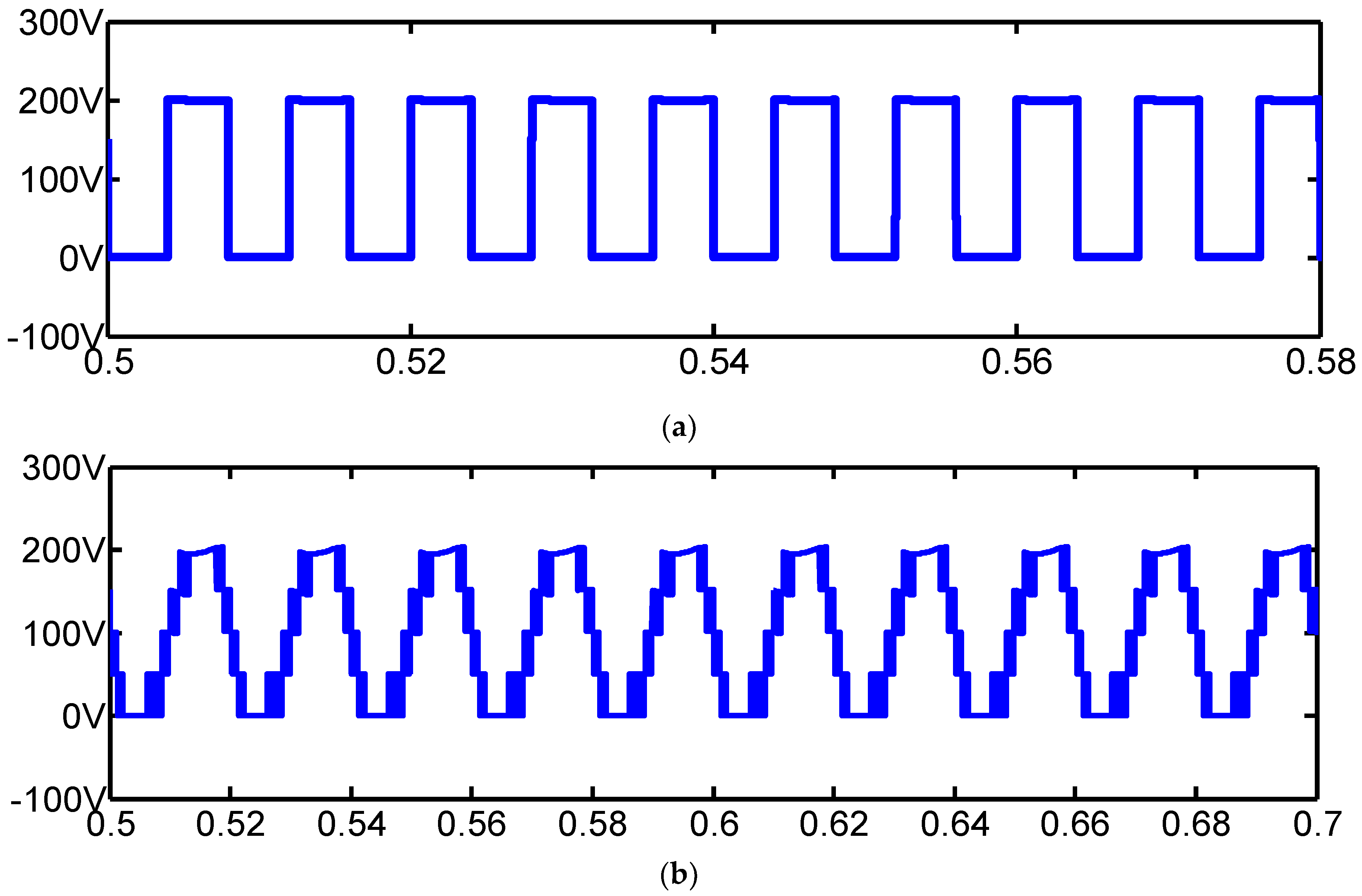
3.1. Modulation Scheme of the Proposed Hybrid MMC

For the MMC system operated under sinusoidal modulation, the SM capacitor voltages were chopped by the power switches during each switching cycle. However, this introduced undesirable switching losses. To overcome this problem, trapezoidal modulation was preferred. As shown in Figure 8, the trapezoidal waveform reference consists of the ramp part and saturation part. The ramp parts in the trapezoidal waveform include the increasing and decreasing parts. The saturation parts include the upper and lower saturation parts. In a specific period, by designing the upper and lower saturation parts of the upper and lower arm voltage references working towards the positive DC bus voltage and zero voltage, respectively, the power switches of the corresponding arm were not switched, dramatically reducing the switching losses. A larger saturation part of the trapezoidal waveform introduces a smaller power loss. Especially, the square waveform, supposed to be the ultimate situation of the trapezoidal waveform when the ramp range disappears, is supposed to perform at a higher efficiency. Likewise, the triangular waveform, supposed to be the other ultimate situation of the trapezoidal waveform when the saturation range disappears, has a worse efficiency. Therefore, trapezoidal modulation is usually designed to improve the efficiency. Despite these merits, it introduces undesirable harmonics for the output voltages, which could damage the power quality. In the proposed hybrid MMC, this issue was suppressed by the SCSM stacks for shaping the output voltages.
For simplification, the saturation rate λ of the trapezoidal waveform is defined as
λ = Δ t s T f / 2
where Δts is the saturation interval of the trapezoidal waveform during half of Tf, and Tf is the period of the trapezoidal waveform. From Equation (11), it is shown that when Δts = 0, the trapezoidal waveform develops into the triangular waveform, while when Δts = Tf/2, the trapezoidal waveform develops into the square waveform. Therefore, the saturation ratio λ is changed between 0 and 1. Once the saturation rate in the trapezoidal waveform is defined, the fundamental frequency component in the trapezoidal waveform is defined. Figure 9 illustrates the relationship of λ and the fundamental frequency component in the trapezoidal waveform. It shows that an increased fundamental frequency component can be produced when the saturation ratio λ is increased. Therefore, the trapezoidal waveform modulation can be used to enlarge the utilization of the DC bus voltage of the proposed hybrid MMC. Theoretically, the square waveform modulation contributes the maximum amplitude of the fundamental frequency component. However, this solution brings an unexpected inrush voltage on the arm reactors in the proposed hybrid MMC. Considering this problem, a compromise of the arm reactor inrush voltage and power loss should be considered when designing a proper λ.
In the upper saturation part of the trapezoidal waveform, the SMs in the corresponding arm are controlled to remain at the inserted state, while in the lower saturation part of the trapezoidal waveform, the SMs in the corresponding arm are controlled to remain at the bypassed state. Therefore, the HBSM capacitor voltage ripples are mostly influenced by the shape of the trapezoidal waveform. When the proposed hybrid MMC operates at the unit power factor under the inverter mode, the HBSM capacitors during the upper saturation part of the trapezoidal waveform have three charging states: firstly charged, then discharged, and finally charged, which is accordant with the shape and direction of the arm current. Therefore, the balancing control is invalid when all the SM capacitor voltages are inserted or bypassed during the saturation part of the trapezoidal arm voltage reference. Thus, the HBSM capacitor voltages could only be balanced during the ramp interval of the trapezoidal waveform. Notice that, although a larger λ results in an enlarged range for the utilization of the DC bus voltage, the smaller interval is reserved for the SM balancing control, which introduces the undesirable inconformity in the HBSM capacitor voltages. Additionally, the inrush parts imposed on arm voltages become serious with larger λ in the proposed hybrid MMC.
When λ reaches its maximum value, the square waveform modulation is illustrated for the proposed hybrid MMC. As shown in Figure 10 of the lower arm voltage and reference, all the HBSM capacitor voltages of the lower arm were inserted to constitute the high level of the lower arm voltage during a half period, while, during the other half period, all the HBSM capacitor voltages of the lower arm were bypassed to constitute the low voltage level of the lower arm voltage. Meanwhile, the HBSM capacitor voltage ripples under inserted states changed with the direction of the lower arm current, while the HBSM capacitor voltages under bypassed states remain unchanged. Specifically, when the lower arm currents were fully above or below zero, the HBSM capacitor voltages under inserted states kept increasing or decreasing theoretically, resulting in an unbalanced feature for the HBSM capacitor voltages. However, by contributing the compensation parts on the lower arm modulation waveform during the low voltage level state, the unbalanced state of the HBSM capacitor voltages can be rectified. By doing so, the HBSM capacitor voltages in the lower arm were modulated during each switching cycle as shown in Figure 11, provoking corresponding power losses. In addition, the derivative influence on reactors from the square waveform modulation was induced. Figure 12 depicts the reactor voltages of the proposed hybrid MMC under the trapezoidal modulation and square modulation, respectively. Compared to the reactor voltage under trapezoidal modulation when λ = 0.5 in Figure 12a, a higher inrush voltage was imposed on the reactor under square waveform modulation in Figure 12b, complicating the reactor insulation design and decreasing the system reliability. Referring to the above analysis, similar results can be obtained for the upper arm of the proposed hybrid MMC.

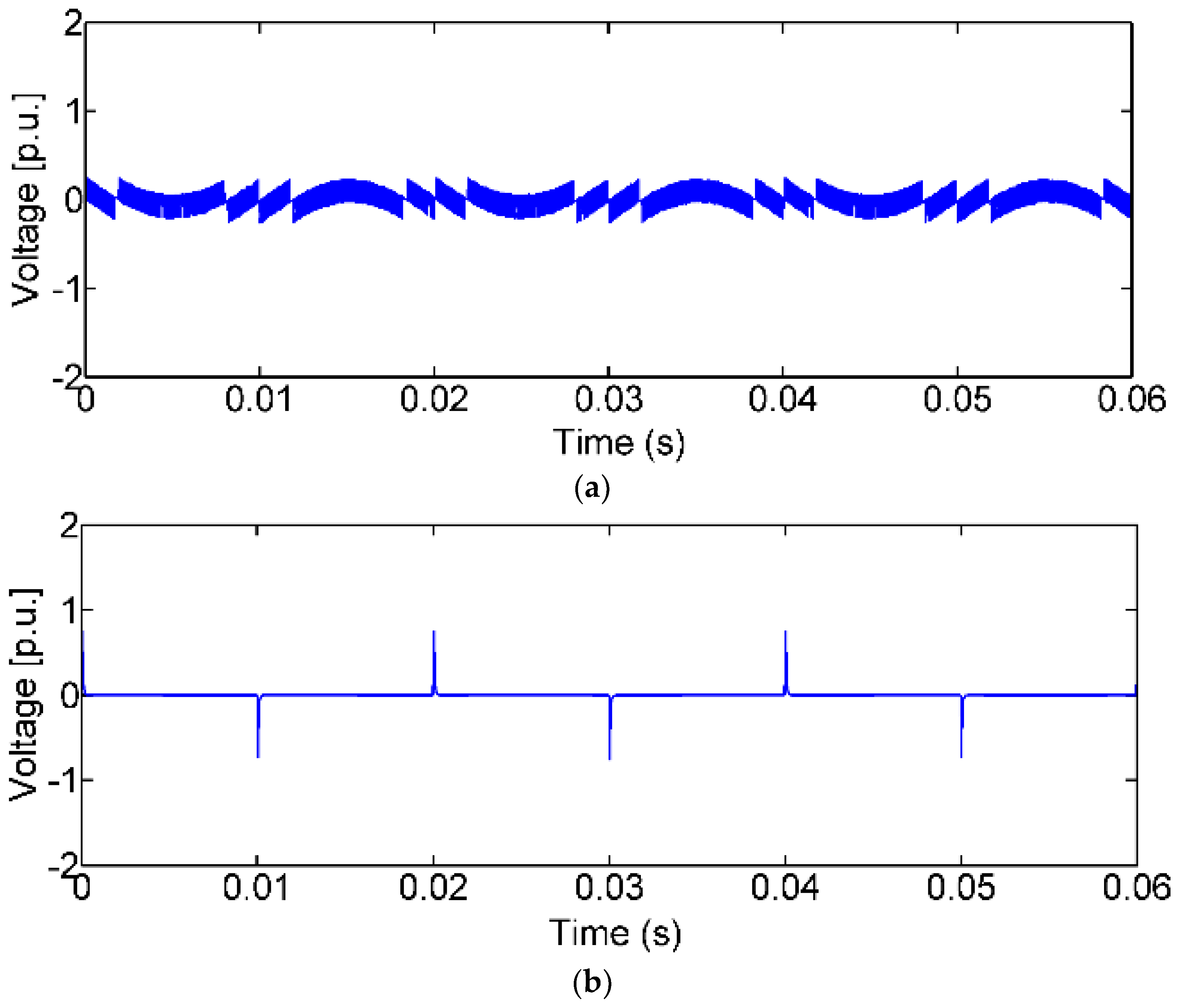
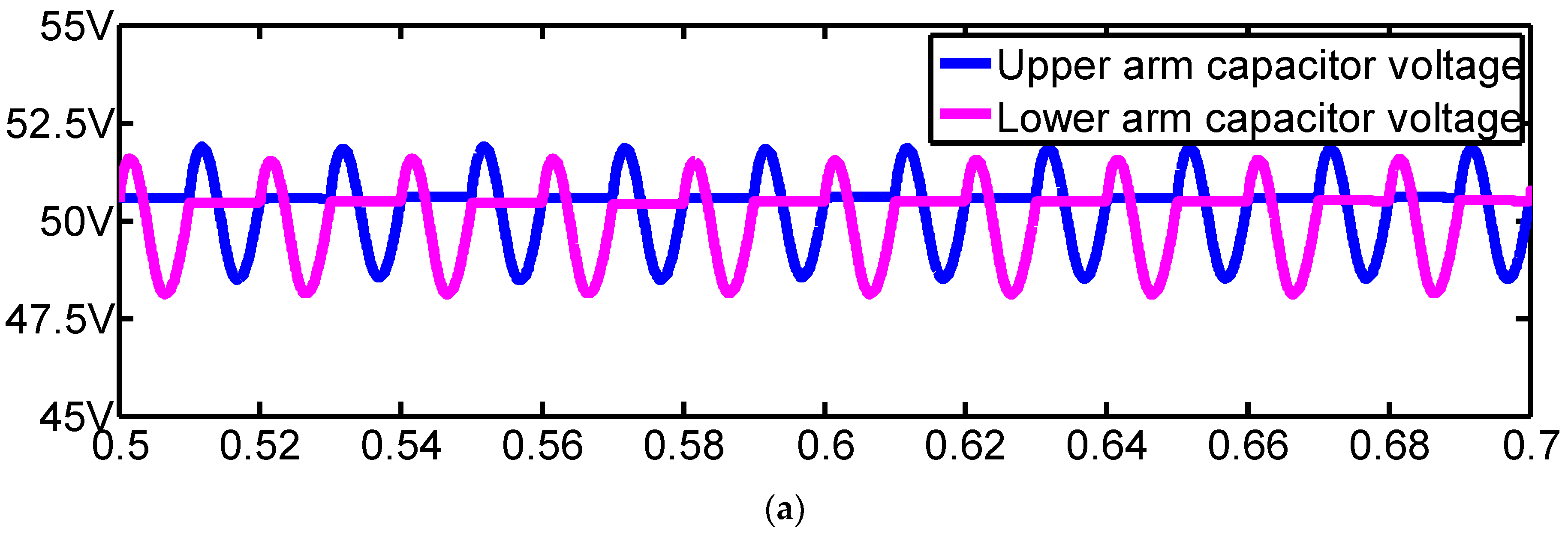
3.2. Analysis and Control of the SCSM Stack

Considering the above-mentioned discussion, applying the trapezoidal modulation with a properly-designed λ was significant in the proposed hybrid MMC. On one hand, the ramp intervals of the trapezoidal waveform provided additional HBSM capacitor voltage sorting time for enhancing the balancing control. On the other hand, a lower inrush reactor voltage can be produced compared to that of the square modulation. Once the trapezoidal waveform modulation was specified for the proposed hybrid MMC, the voltage reference for the SCSM stack could be defined. As shown in Figure 13 of the modulation process in the proposed hybrid MMC, despite the above-mentioned merits, the trapezoidal waveform had a lower peak value compared to the pure sinusoidal waveform when containing the same fundamental frequency component.
In the proposed hybrid MMC, the balancing control of the SCSM stack was different from that of the HBSM stacks. For the HBSM stack, since there is only one capacitor in a single HBSM, the instantaneous HBSM power is equal to that of the HBSM capacitor. Thus, once the average power of the single HBSM remains zero, the HBSM capacitor voltage can be balanced. As for the SCSMs, due to the reason that there are two capacitors in a single SCSM, the instantaneous SCSM power is the sum of the instantaneous powers of the two SCSM capacitors in a single SCSM, which could not ensure the balance states of the SCSM capacitor voltages. Only if each of the SCSM capacitor voltages is balanced, the SCSM can be balanced. Therefore, the average control and individual control for the SCSM capacitor voltages were proposed. The average control aimed to achieve the overall balancing state of the SCSM, while the individual control was used for each SCSM capacitor voltage.
For analyzing the balancing characteristics of the SCSMs, it was necessary to investigate the instantaneous powers of the SCSM stacks. Generally, the SCSM stack is in charge of shaping the output voltage, which does not produce any fundamental frequency component. Meanwhile, due to the reason that the current flowing through the SCSM stack is equal to the output current, the instantaneous power of the SCSM stack does not contain any DC components, resulting in the balanced state for the sum of the SCSM capacitor powers. Therefore, this verified the feasibility of the average control for the SCSM stack.
For the individual control of the SCSM capacitor voltage, it was achieved by the fact that the average power of each SCSM capacitor remained zero. Theoretically, the balanced states of the SCSM capacitor voltages can be defined by the SCSM capacitor currents. When the SCSM capacitor current only contains alternative current component, the SCSM capacitor voltages can be balanced. According to the structure of the SCSM, the upper and lower SCSM capacitor currents can be expressed as
{ i x u p = 1 2 ( 1 + u x s c r e f 2 U r e f ) i x = 1 2 i x + u x s c r e f 4 U r e f i x i x l o w = 1 2 ( 1 u x s c r e f 2 U r e f ) i x = 1 2 i x + u x s c r e f 4 U r e f i x
where ixup and ixlow are the upper and lower SCSM capacitor currents, respectively, uscref is the reference of the SCSM voltage, and Uref is the reference of the SCSM capacitor voltage. Since the SCSM reference voltage uxscref contains no fundamental frequency part, there is no DC component involved in the SCSM capacitor currents in (12). Thus, the balancing states of the SCSM capacitor voltages in theoretical feasibility can be ensured. Specifically, from (12), it shows that the output current is evenly split between the upper and lower SCSM capacitor currents. In addition, the higher frequency components produced by the second terms in the right hand of ixup and ixlow in (12) are equally distributed in ixup and ixlow. Based on (10), the upper and lower SCSM capacitor voltages can be derived as
{ u x u p = U r e f + 1 C t 0 t 1 2 ( 1 + u x s c r e f 2 U r e f ) i x d t u x l o w = U r e f 1 C t 0 t 1 2 ( 1 u x s c r e f 2 U r e f ) i x d t  
where uxup and uxlow are the upper and lower SCSM capacitor voltages, respectively. Equation (13) shows that the upper and lower SCSM capacitor voltages consist of the reference part, the fundamental frequency part, and the higher frequency parts. The fundamental frequency parts of uxup and uxlow in Equation (13), supposed to be dominant in SCSM capacitor voltage ripples, have the same amplitude with opposite signs. For the higher frequency parts in SCSM capacitor voltage ripples, the amplitudes of the harmonics attenuate greatly, which have slight influence.
Figure 14 illustrates the structure diagram of the balancing control for SCSM, which consisted of the average control and the individual control. In Figure 14a, the sum of the upper and lower capacitor voltages in SCSM was designed to track the voltage reference. When it deviated from the voltage reference, the active powers were absorbed from the output current for suppressing the deviation. Meanwhile, the individual control in Figure 14b ensured that each SCSM capacitor voltage could be controlled to vary around its reference voltage. When the SCSM capacitor voltage is higher than its reference, the compensation part Δuxycap attempts to reduce the charge time during the positive period of ix, or to enlarge the discharge time during the negative period of ix. When the SCSM capacitor voltage is lower than its reference, the compensation part Δuxycap attempts to enlarge the charge time during the positive period of ix or to reduce the discharge time during the negative period of ix.
Considering the compensation parts of the SCSM control in Figure 14, the voltage references of the SCSM stacks should be modified. Substituting the corresponding compensation parts into Equation (10), the modified voltage reference of SCSM can be expressed as
u x s c i = u x s c r e f j + Δ u x u c a p + Δ u x l c a p + Δ u x c a p
where uxsci is the voltage reference of the i-th SCSM in phase x (x = a, b, c), Δuxycap (y = u, l) is the compensation part of the balancing control, and Δuxcap is the compensation part of the average control of phase x (x = a, b, c).
To guarantee the accurate realization of the SCSM voltages referenced by (14) and the superior uniformity of the SCSM capacitor voltages, the phase-shifted carrier PWM (PSC-PWM), featured by the evenly distributed harmonics and the highly performed voltage quality of the SCSM voltages, was adopted to control the cascaded SCSM stacks. The modulation process of the SCSM stack under PSC-PWM is illustrated in Figure 15. For the proposed hybrid MMC system equipped with j SCSMs on the AC side, the voltage modulation reference for each SCSM can be defined as uxsref/j. Concomitantly, the triangular carriers of the j SCSMs should be shifted by 2π/j in sequence to achieve the harmonic cancellation of the SCSM voltages.
Additionally, the whole control diagram of the proposed hybrid MMC is depicted in Figure 16. It consists of the control structures of the HBSM stacks and SCSM stacks. To regulate the active powers, the average control of the HBSM stacks in the main converter with an outer voltage loop and an inner current loop was proposed. Then, the corresponding compensation parts were sent to the modulation process to cooperate with the individual control of the HBSMs and the trapezoidal waveform generator, for synthesizing the required modulation signals of the HBSM stacks.

3.3. Fault Blocking Capability of the Proposed Hybrid MMC

Taking the bipolar DC short circuit fault for analysis, when the DC fault occurs, the rapid discharge of the SM capacitors is the key factor for causing the inrush fault current. Therefore, the detective signals of the fast drop on SM capacitor voltages or the rapid increase on arm currents would be significant for triggering the protection process. Generally, a robust MMC system with fault blocking capability should cut off the fault current before it damages the power semiconductors. However, for the traditional HBSM-based MMC, the anti-parallel diodes of the IGBTs, imposed by the inverse voltages, are forced to be switched on, being restricted for the overhead line HVDC applications.
For the proposed hybrid MMC, the SCSM stack on the AC side supplied a possible way for blocking the fault current. The fault current route could be changed by shutting all the IGBTs, which is described in Figure 17. As it can be observed, one of the split capacitor voltages was always inserted in the fault current route. Therefore, when the SCSM number is accordant with the fault blocking requirement, the antiparallel diodes in fault current route can be controlled to stand the inverse voltages, which should obey
3 U m < 2 j U s c s m
where Um is the amplitude of the AC phase voltage, and Usccm is the reference of SCSM capacitor voltage. Therefore, based on Equation (15), the SCSM number can be designed by
j > 3 U m 2 U s c s m

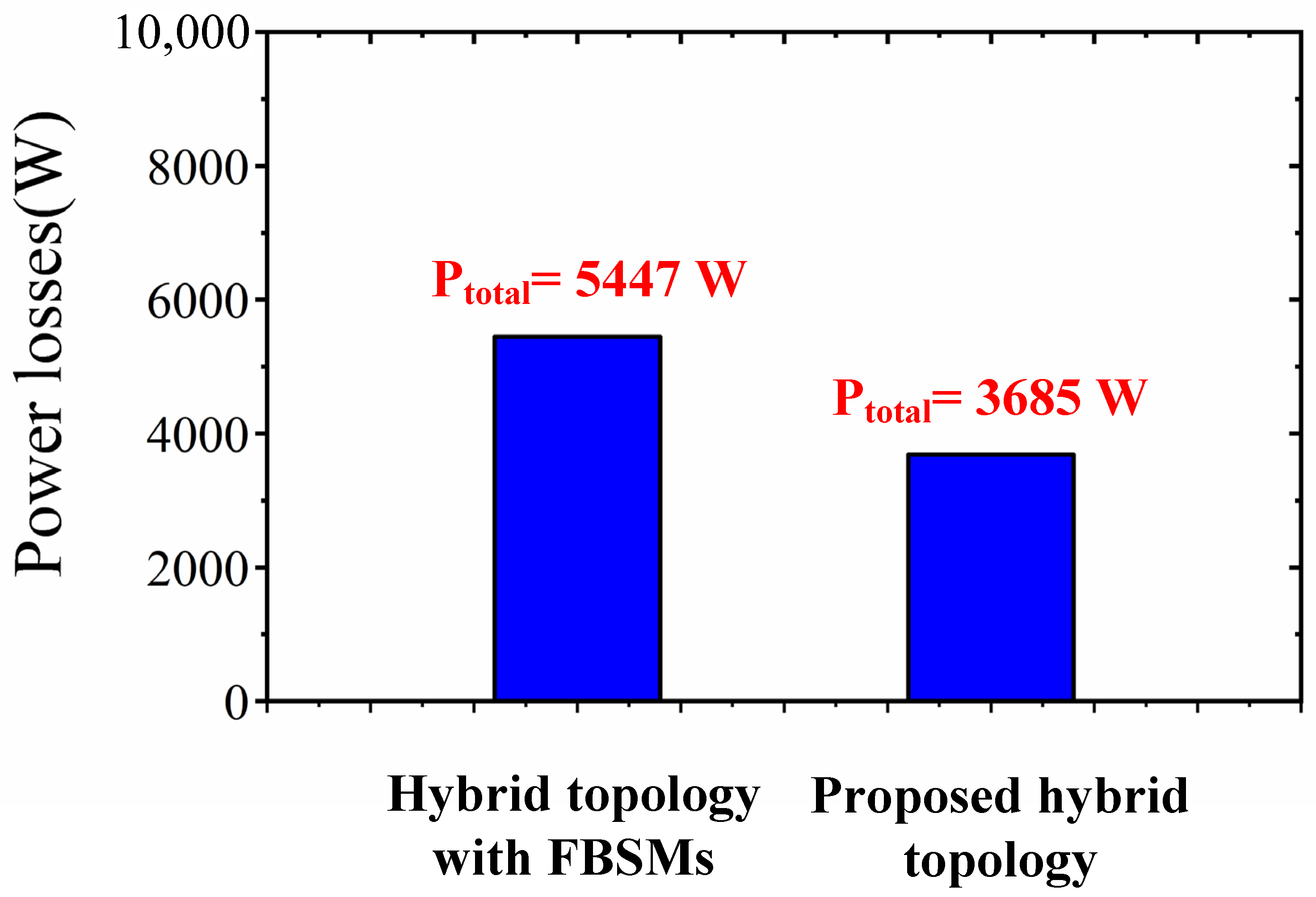
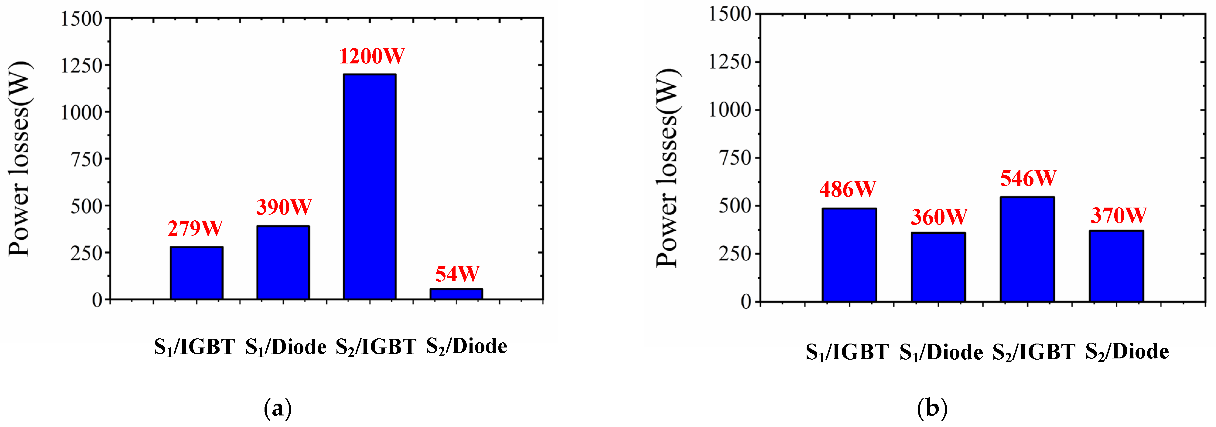
3.4. Power Losses Analysis of the Proposed Hybrid MMC

Profited by the trapezoidal modulation and the proposed SCSM stacks, the power losses of the proposed converter could be significantly reduced. To estimate the loss performance of the proposed converter, the hybrid MMC with FBSMs on the AC side (shown in Figure 1) was employed for loss comparison. To achieve a fair comparison, identical simulation parameters were adopted for these two MMC converters, as listed in Table 2. The power modules for each SM of the MMC converters were Infineon FF150R12ME3G (Tj = 125 °C, Vge = 15 V). To obtain the superior evaluation in terms of efficiency, the power losses of the MMCs were calculated in the assumption of running at rated parameters of the selected power modules.
Figure 18 depicts the total power losses of the compared MMC topologies. The power losses of each converter consisted of conduction losses and switching losses. It showed that the lower loss could be achieved for the proposed hybrid MMC. Additionally, the power loss distributions of the SMs in the proposed hybrid MMC are also derived in Figure 19. While Figure 19a shows the power loss distribution of the total HBSM stacks, Figure 19b shows the power loss distribution of the total SCSM stacks. In Figure 19a, it shows that the losses were unevenly distributed among the semiconductor devices of the HBSMs, and the IGBTs S2 of the HBSMs suffered the majority of the HBSM losses. As for the losses of the semiconductor devices in the SCSMs, the relatively even distribution of the power losses, illustrated in Figure 19b, could be achieved due to the harmonic powers of the SCSM stacks having symmetrical distribution in SCSM power switches.

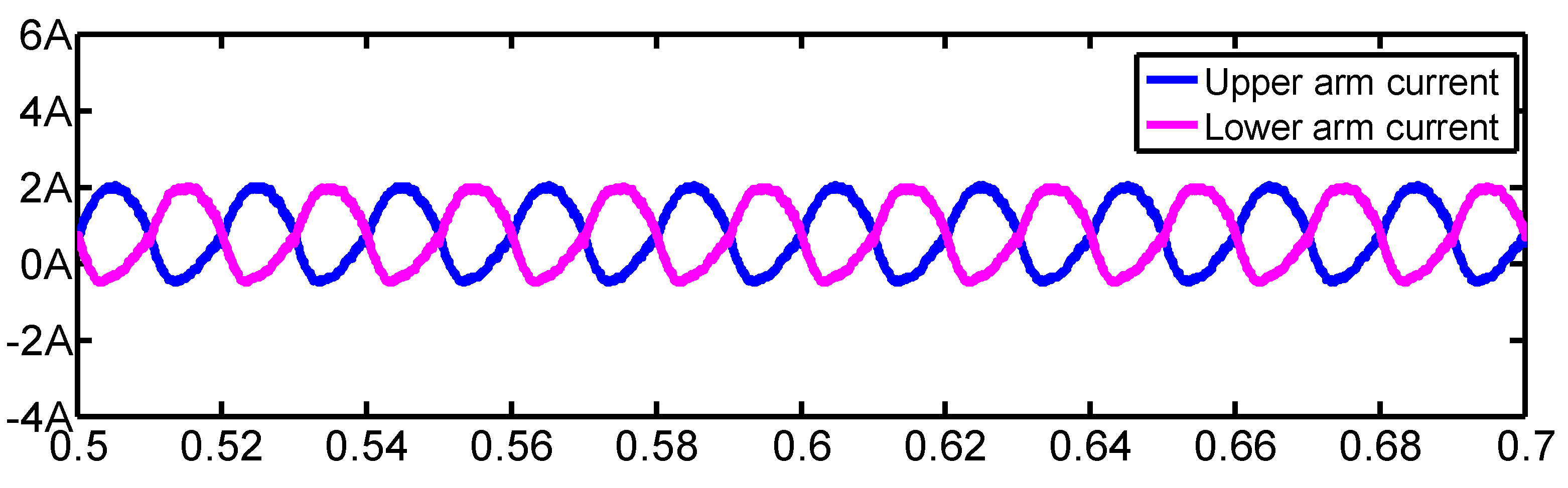
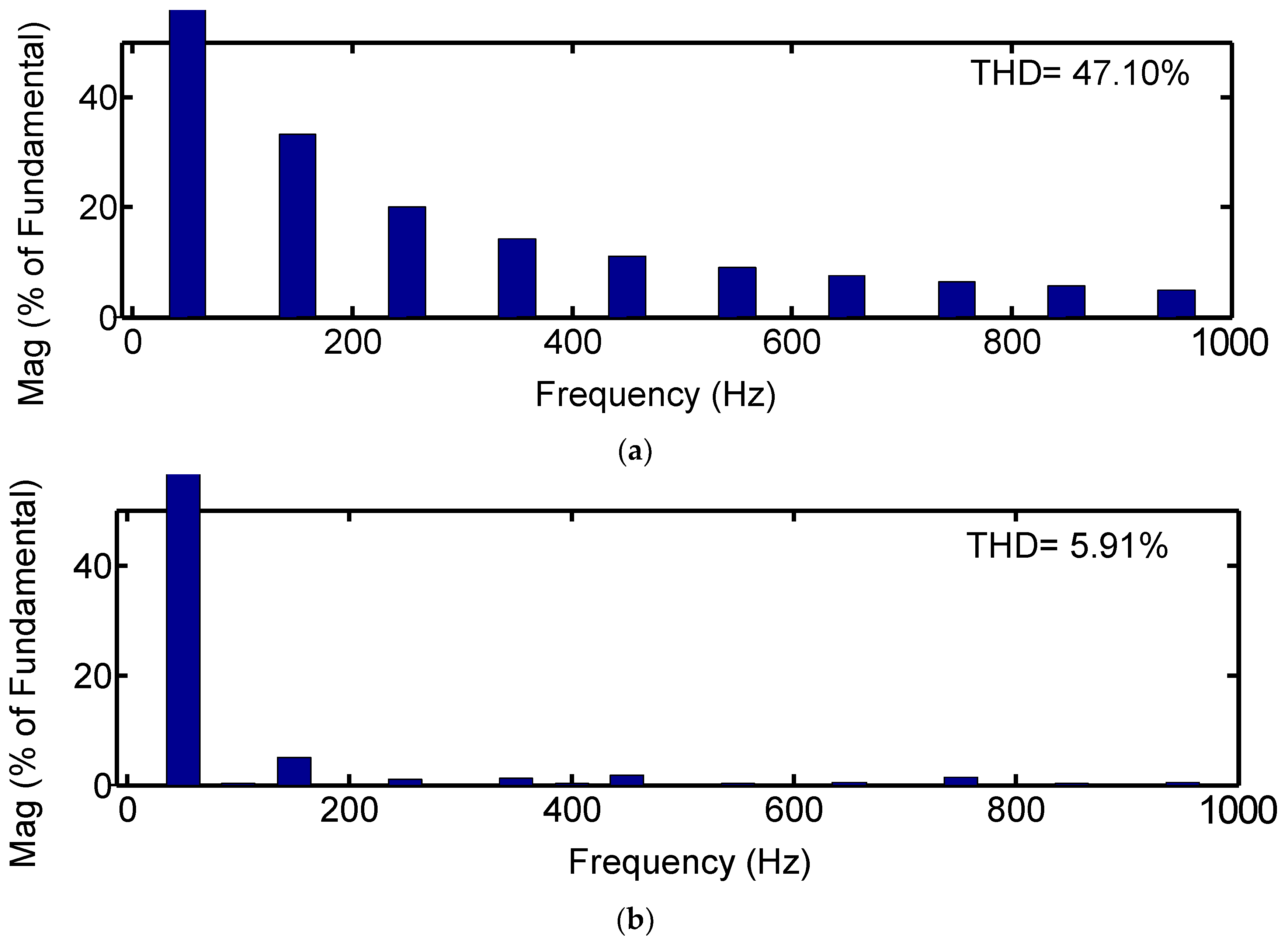
4. Simulation Results

The basic operation principle and control of the proposed hybrid MMC were discussed in detail in Section 2 and Section 3. Theoretical analysis showed that enlarged realization of the DC bus voltage under smaller power losses in the proposed hybrid MMC can be achieved, which was also enabled to block the DC fault current. This section gives the corresponding simulation results to verify the effectiveness of the discussion under MATLAB/Simulink. Meanwhile, aiming to obtain superior waveforms and evenly distributed SM harmonics of the HBSM and SCSM stacks, the phase-shifted carrier PWM (PSC-PWM) was adopted in the simulation process. Detailed parameters are listed in Table 3.
As discussed in Section 3, the HBSM capacitor voltage ripples in the proposed hybrid MMC were influenced by the modulation waveforms and the arm currents. Figure 20 illustrates the HBSM capacitor voltages of the proposed hybrid MMC under different λ. Figure 20a is the HBSM capacitor voltage when λ = 1, while Figure 20b is the HBSM capacitor voltage when λ = 0.5. As depicted, the HBSM capacitor voltage ripples can be divided into two parts during one fundamental period, which can be defined as the unchanged interval and the charging interval. In the unchanged interval, all the HBSMs of the corresponding arm are controlled to be switched off and the HBSM capacitor voltages remain unchanged. Therefore, the balancing control and power exchange are not available during the unchanged interval. In the charging interval, the balancing control and the power exchange are available. In addition, the corresponding changes on the arm voltages are provided. As shown in Figure 21, the HBSMs are not modulated during the upper and lower saturation parts of the arm voltages, which shows accordance with the variation in the HBSM capacitor voltages.
To further investigate the performance of the proposed topology, the arm instantaneous powers are also illustrated. As depicted of the conditions under different λ, Figure 22a is the arm powers of the proposed topology under λ = 1, while Figure 22b is the arm powers of the proposed topology under λ = 0.5. In Figure 22a, it can be observed that both of the upper and lower arm powers were not changed during almost half of the fundamental period when λ = 1, and the non-exchanged intervals for the upper and lower arm powers were shifted by half of the fundamental period. In Figure 22b, when λ was decreased, it shows that the non-exchanged intervals for the upper and lower arm powers were also decreased, which is different from the power exchanging principle for the MMC system operated under sinusoidal waveform modulation control.
Figure 23 illustrates the arm currents of the proposed hybrid MMC when λ = 0.5. It can be observed that the arm currents mainly consisted of the DC component and the fundamental component. The DC components of the arm currents aimed to achieve the power transmission, while the fundamental components contributed to the load current. In addition, the shape of the arm current influences the shape of the HBSM capacitor voltage since the HBSM capacitor is charged by the arm current during the charging interval.
The SCSM stack in the proposed hybrid MMC, serving as the harmonic generator, aimed to reshape the output voltage. The SCSM capacitor voltages and currents of the proposed hybrid MMC when λ = 0.5 are illustrated in Figure 24. In Figure 24a, it shows that the upper and lower SCSM capacitor voltage ripples mainly contained the fundamental frequency parts with opposite signs, which were mainly caused by the SCSM capacitor currents in Figure 24b. Moreover, it also can be observed that the SCSM capacitor currents had the outer shape of the output current, which were derived from modulating the output current by the driven signals produced in Equation (14). The characteristics in Figure 24 are in accordance with the discussions in Equations (12) and (13).
For a fair comparison, the output voltages operating at different MMC topologies when λ = 0.5 are illustrated in Figure 25. Figure 25a is the output voltage of a traditional MMC topology with trapezoidal modulation, while Figure 25b is the output voltage of the proposed topology with trapezoidal modulation. It shows that the trapezoidal output voltage can be efficiently shaped by the proposed SCSM stack. The spectrum distribution of Figure 25 is also illustrated in Figure 26. As depicted, the THD of the output voltage dramatically improved from 11.63% to 4.8%. Similar simulation results of the output voltages for different MMC topologies when λ = 1 are shown in Figure 27. Compared to the square modulation, the reactor inrush voltages can be extremely suppressed when λ is far below the unit. Figure 28 shows the spectrum distribution of the output voltages in Figure 27, obtaining a significant improvement of the output voltage quality.

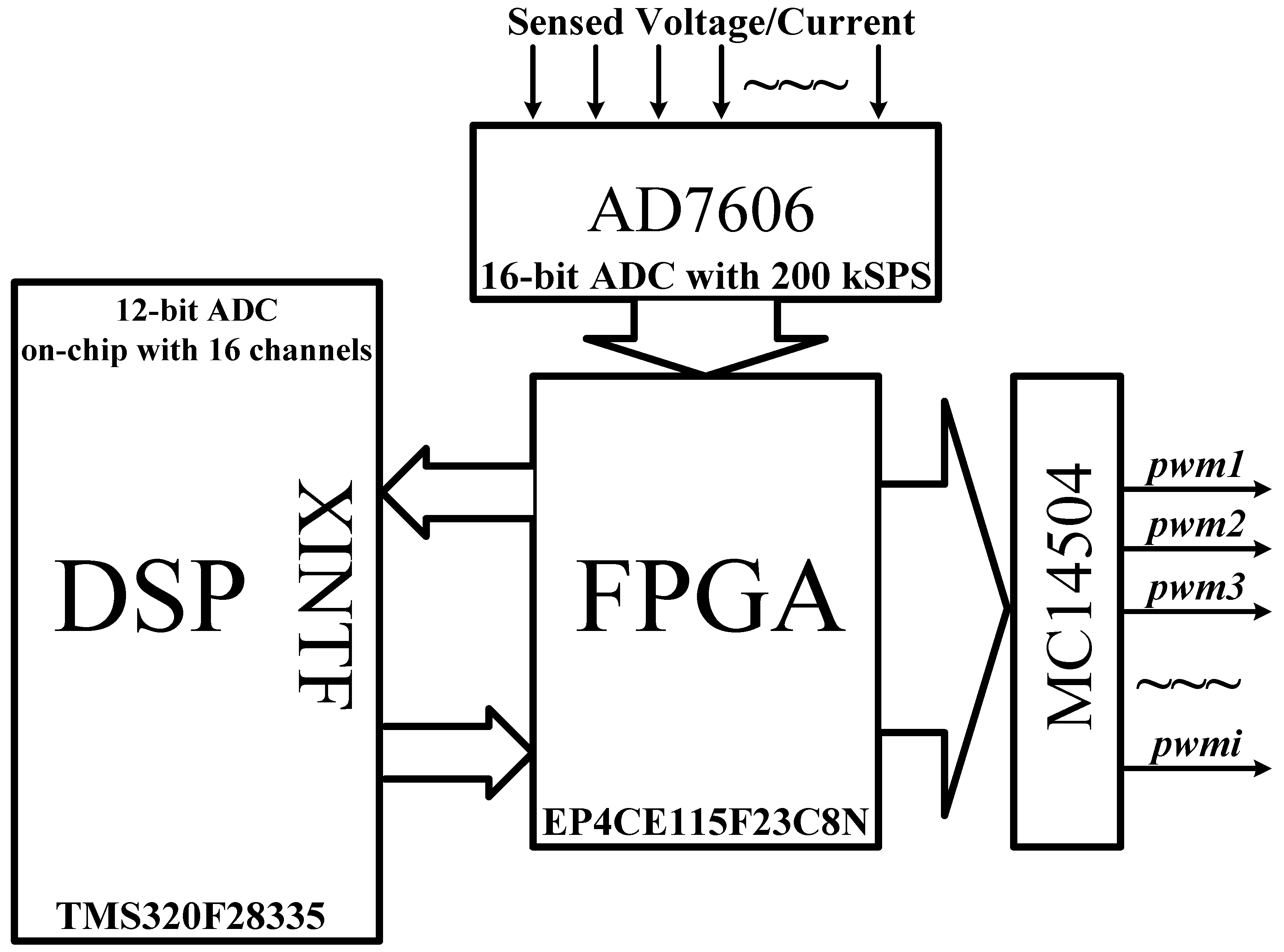
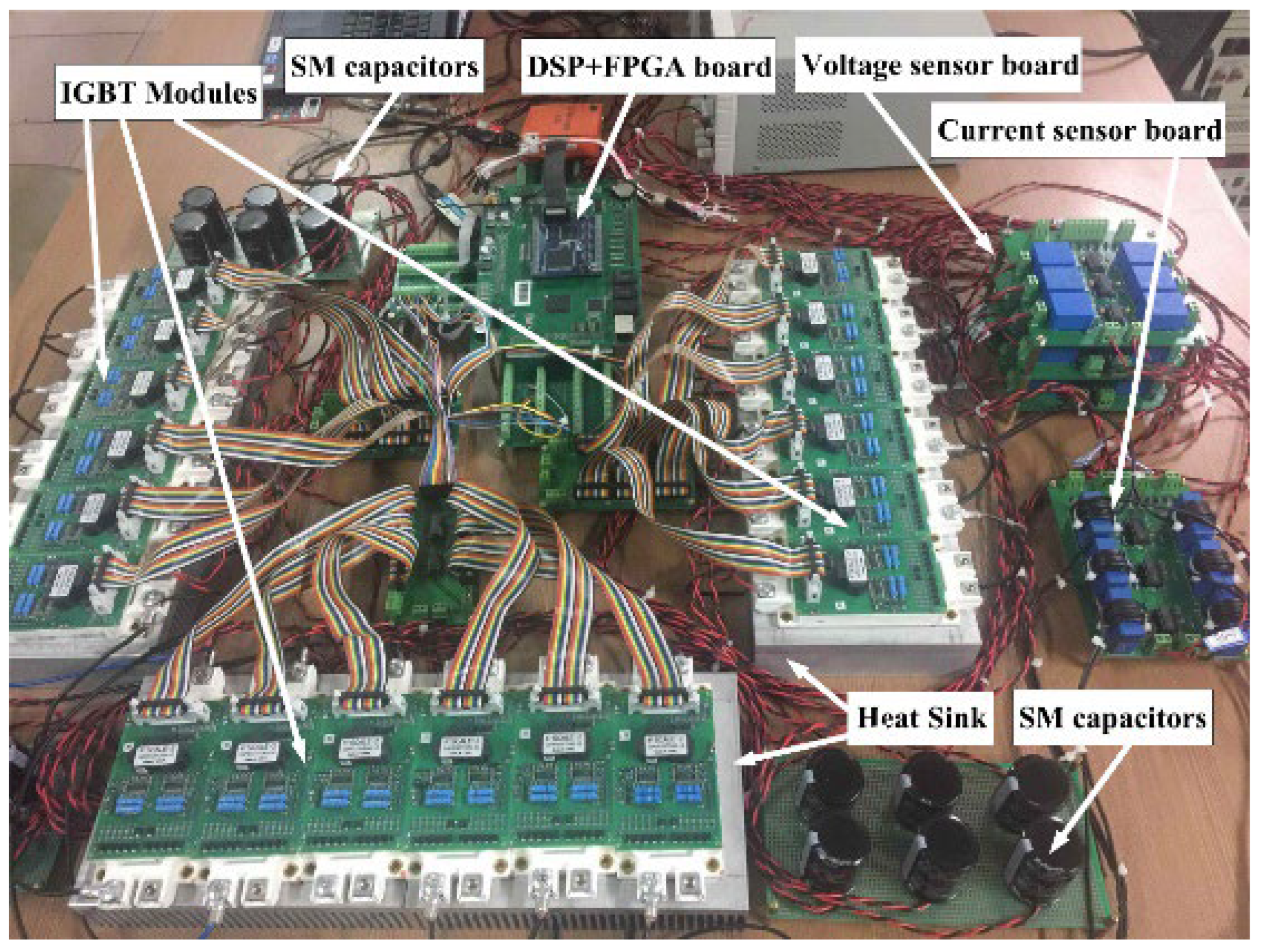
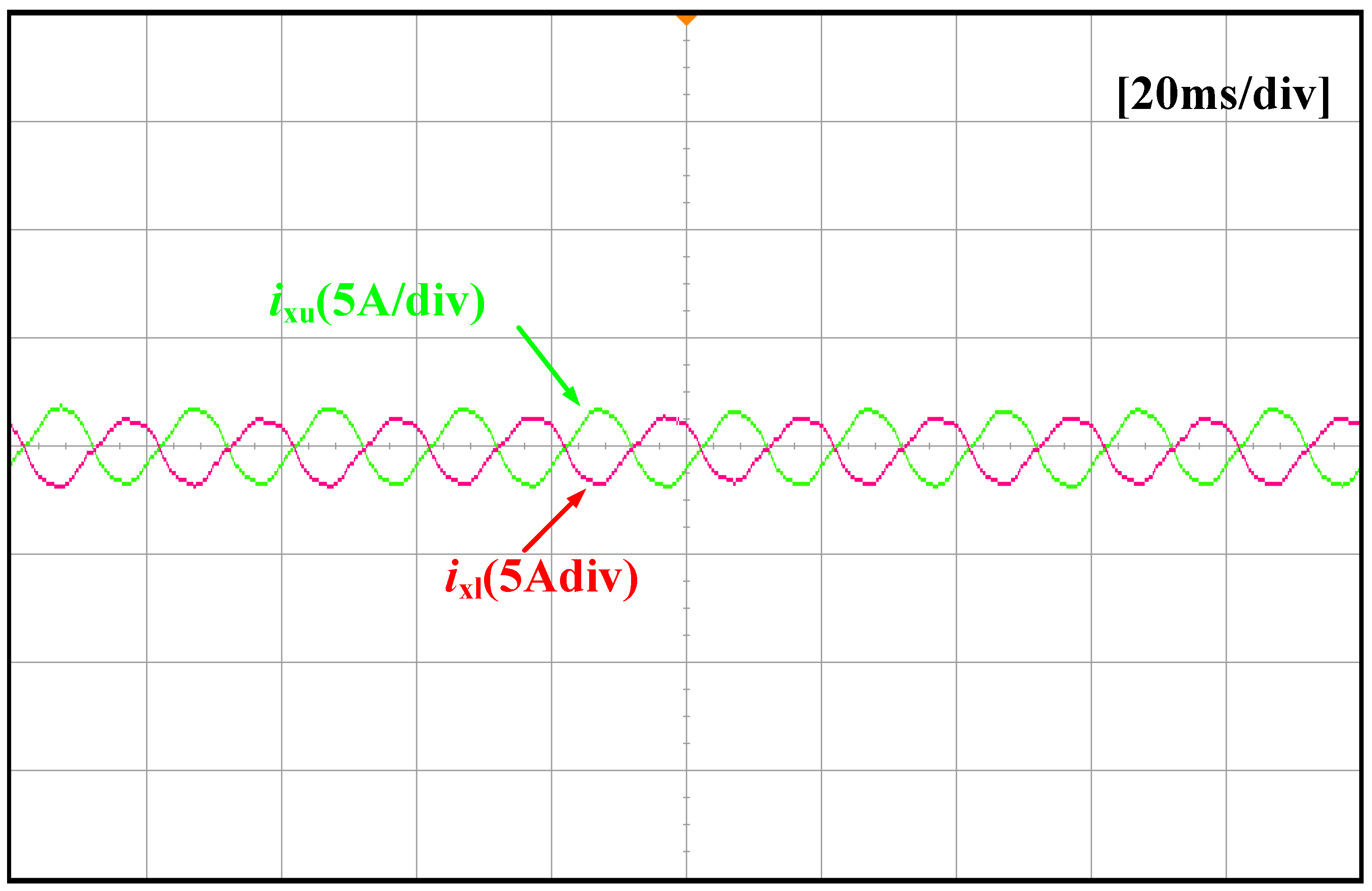
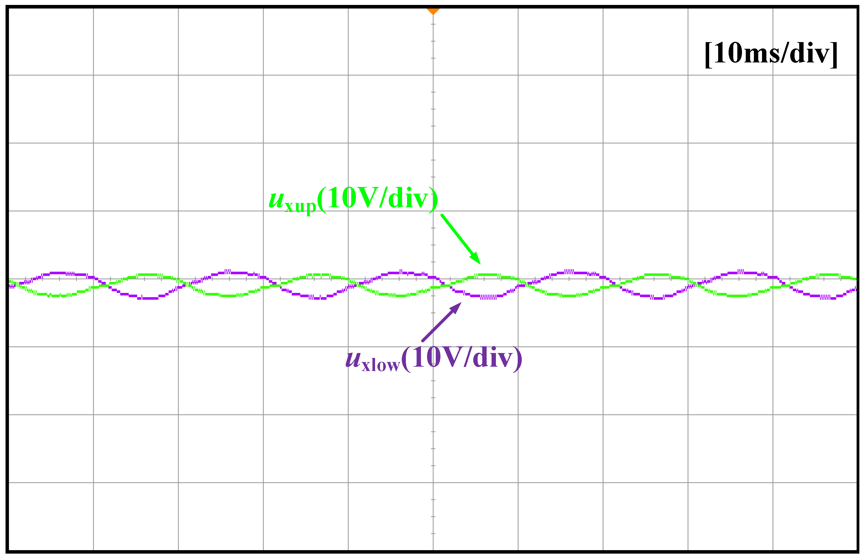
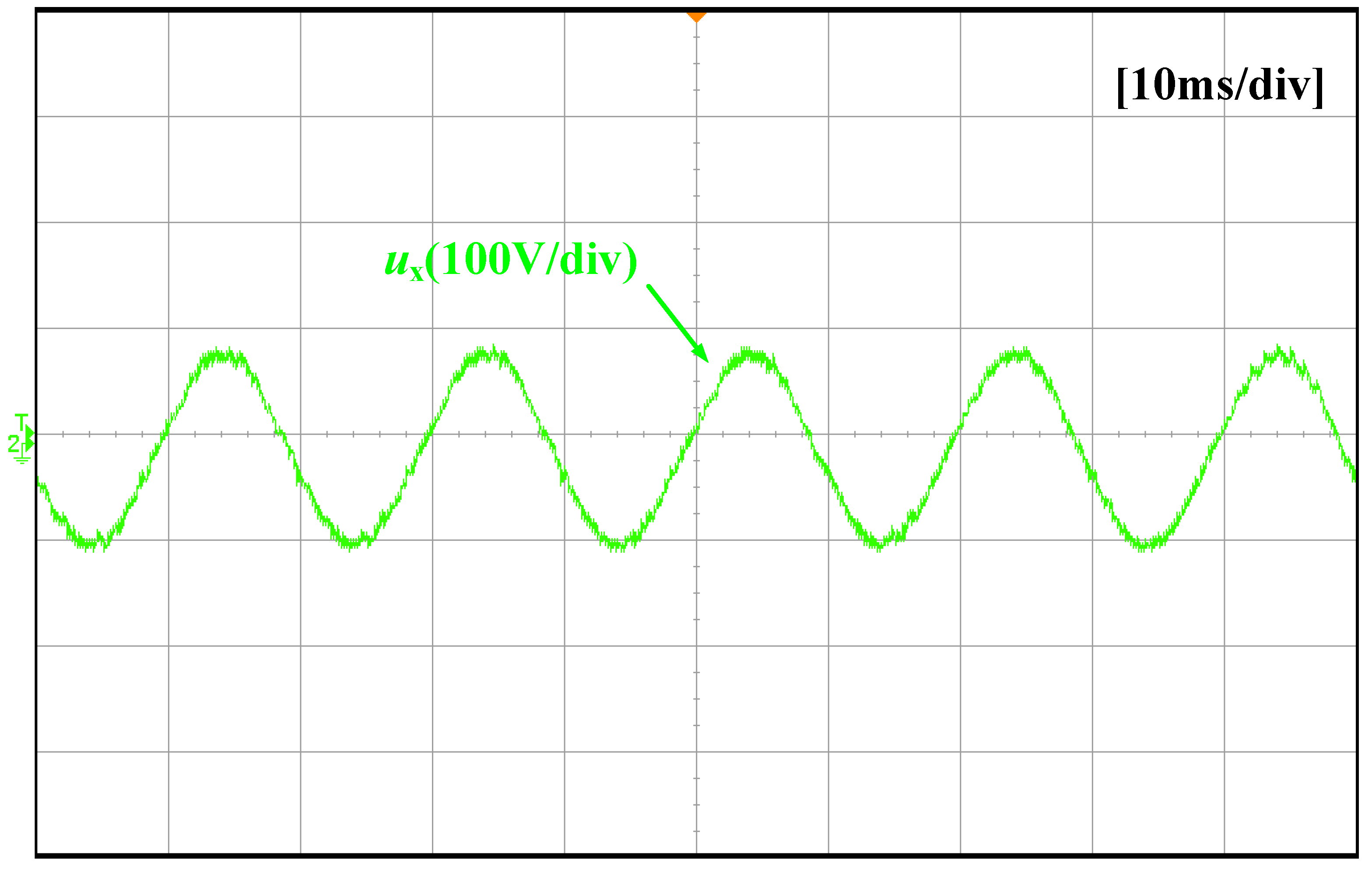
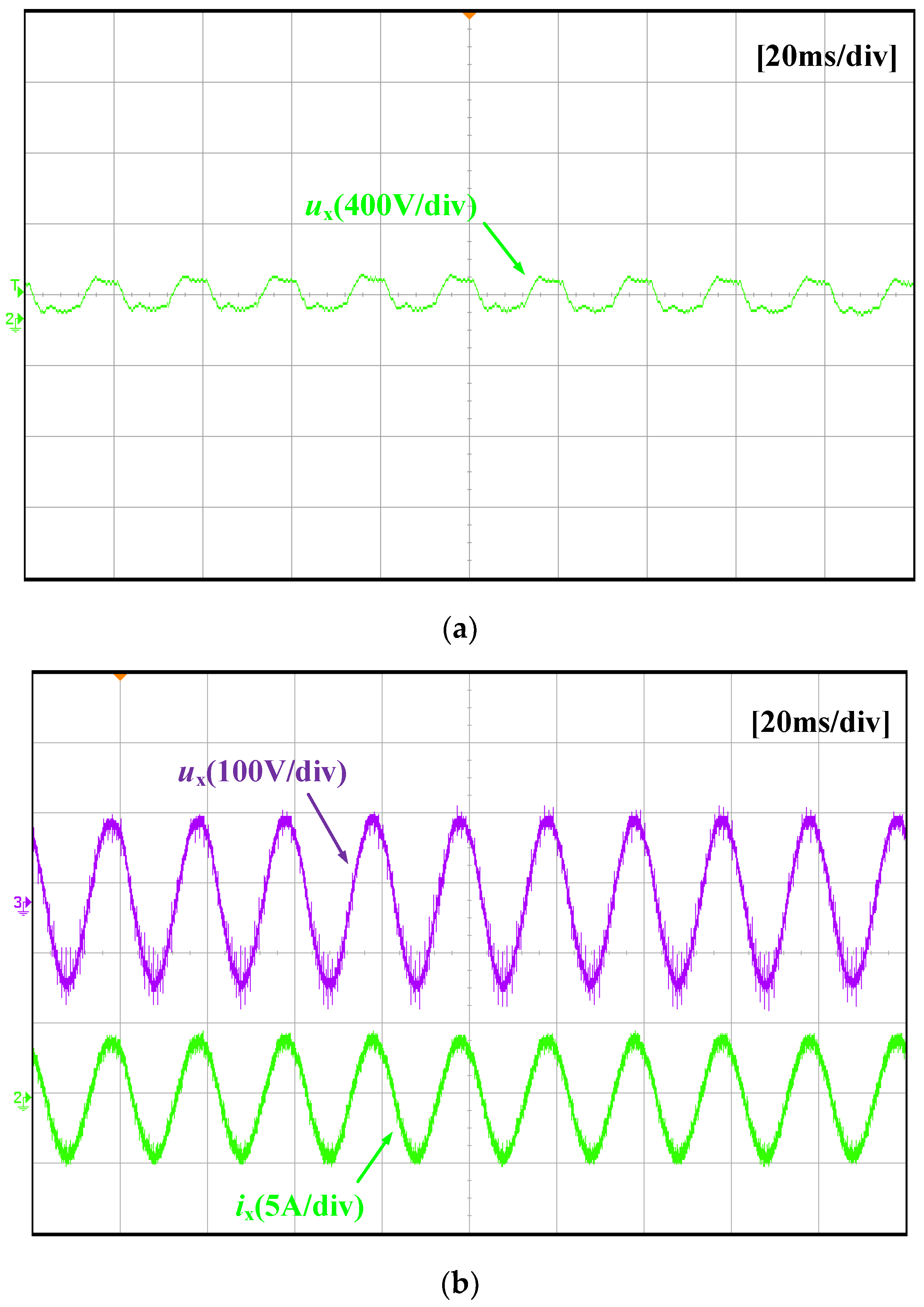
5. Experimental Results

The proposed hybrid MMC aims to achieve the enlarged utilization of DC bus voltage with smaller power losses compared to the FBSM-based hybrid MMC, which, in the meantime, is capable of blocking the DC fault current. For further identifying the effective performance of the proposed hybrid MMC, a downscaled prototype of the power stage was built to verify the effectiveness of the theoretical analysis and discussion in Section 2. Considering the limitation of the experimental facilities, the monophase power stage with four SMs per arm and two SCSMs on the AC side was established. The basic structure of the proposed hybrid MMC is shown in Figure 29, which is composed of the main power stage and control stage. Notice that the DC voltage source in the main power stage was built by an uncontrollable rectifier. The control system consists of the TI-tms320f28335 DSP and Altera EP4CE115F23C8N FPGA chips. As shown in Figure 30, The DSP chip was set as the host position for achieving the control algorithm, while the FPGA board mainly took charge of collecting the sampled signals and distributing the PWM signals. A photograph of the experimental stage is depicted in Figure 31. Corresponding parameters for the experiment are listed in Table 4.
To verify the effectiveness of the proposed hybrid MMC, the experimental results when λ = 0.25 are provided. The HBSM capacitor voltage is shown in Figure 32. As illustrated in Figure 32, an unchanged interval exists in the HBSM capacitor voltage during one fundamental period. While during the rest time of the unchanged interval, the waveform shape of the HBSM capacitor voltage ripple is mainly influenced by the arm current. The arm currents of the proposed hybrid MMC are shown in Figure 33. It shows that the arm currents mainly consist of the DC and fundamental frequency components.
The SCSM capacitor voltages of the proposed hybrid MMC are illustrated in Figure 34. It can be observed that the upper and lower SCSM capacitor voltages have the inverse shape feature, which is mainly caused by the specific split structure. Finally, the output voltage of the proposed hybrid MMC is also provided in Figure 35, which reflects that the undesirable harmonics can be mostly suppressed.
Additionally, a comparison of the experimental results for different MMC topologies under enlarged output conditions when λ = 0.5 is presented in Figure 36. As illustrated, Figure 36a is the output voltage waveform of traditional MMC topology with trapezoidal modulation, while Figure 36b is the output waveforms of the proposed MMC topology with trapezoidal modulation. As it is observed from Figure 36, the output waveforms can be significantly improved by the proposed topology.

6. Conclusions

This paper proposed a hybrid MMC topology equipped with split-capacitor-based sub-modules (SCSMs) on the AC side. It was intended to achieve power transmission by providing DC fault blocking capability with enlarged utilization of the DC bus voltage. The proposed SCSM could not only serve as the harmonic generator for filtering the output voltages but could also supply an inverse voltage source for cutting off the DC fault current. Meanwhile, due to the specific design of the SCSM structure, there was only one power semiconductor of the SCSM in the current flow route, which extremely reduced the conduction losses compared to that of the hybrid MMC system equipped with FBSM stacks on the AC side. Additionally, for further reducing the system losses of the proposed hybrid MMC, the trapezoidal modulation with properly designing λ was introduced. Different saturation rates of the trapezoidal modulation were also discussed, and the outcome suggests that a compromise should be made between the power losses and reactor voltages. A corresponding mathematic model of the proposed hybrid MMC was provided and analyzed. The control strategy and design process of the SCSM were also presented. Finally, the simulation and experimental results were employed to verify the effectiveness of the theoretical analysis.

Author Contributions

Conceptualization, M.H.; methodology, M.H.; software, M.H.; validation, M.H. and J.L.; formal analysis, M.H.; investigation, M.H.; resources, M.H.; data curation, M.H.; writing—original draft preparation, M.H.; writing—review and editing, J.L.; visualization, M.H.; supervision, M.H.; project administration, M.H.; funding acquisition, M.H. All authors have read and agreed to the published version of the manuscript.

Funding

This research was supported by the Nature Science Basic Research Plan in Shaanxi Province of China under Grant number: 2021JQ-115.

Institutional Review Board Statement

Not applicable.

Informed Consent Statement

Not applicable.

Conflicts of Interest

The authors declare no conflict of interest.

References

  1. Lesnicar, A.; Marquardt, R. An innovative modular multilevel converter topology suitable for a wide power range. In Proceedings of the IEEE Bologna Power Tech Conference Proceedings, Bologna, Italy, 23–26 June 2003; Volume 3, p. 6. [Google Scholar] [CrossRef]
  2. Glinka, M.; Marquardt, R. A New AC/AC Multilevel Converter Family. IEEE Trans. Ind. Electron. 2005, 52, 662–669. [Google Scholar] [CrossRef]
  3. Glinka, M. Prototype of multiphase modular-multilevel-converter with 2 MW power rating and 17-level-output-voltage. In Proceedings of the 2004 IEEE 35th Annual Power Electronics Specialists Conference (IEEE Cat. No. 04CH37551), Aachen, Germany, 20–25 June 2004. [Google Scholar] [CrossRef]
  4. Akagi, H. Classification, Terminology, and Application of the Modular Multilevel Cascade Converter (MMCC). IEEE Trans. Power Electron. 2011, 26, 3119–3130. [Google Scholar] [CrossRef]
  5. Huang, M.; Zou, J.; Ma, X. Hybrid Modular Multilevel Converter with Redistributed Power to Reduce Submodule Capacitor Voltage Fluctuation. IEEE Trans. Power Electron. 2018, 33, 6595–6607. [Google Scholar] [CrossRef]
  6. Korn, A.J.; Winkelnkemper, M.; Steimer, P. Low output frequency operation of the Modular Multi-Level Converter. In Proceedings of the 2010 IEEE Energy Conversion Congress and Exposition, Atlanta, GA, USA, 12–16 September 2010; pp. 3993–3997. [Google Scholar]
  7. Hagiwara, M.; Nishimura, K.; Akagi, H. A Medium-Voltage Motor Drive with a Modular Multilevel PWM Inverter. IEEE Trans. Power Electron. 2010, 25, 1786–1799. [Google Scholar] [CrossRef]
  8. Zhang, M.; Huang, L.; Yao, W.; Liu, Z. Circulating Harmonic Current Elimination of a CPS-PWM-Based Modular Multi-level Converter with a Plug-in Repetitive Controller. IEEE Trans. Power Electron. 2014, 29, 2083–2097. [Google Scholar] [CrossRef]
  9. Yang, L.; Li, Y.; Li, Z.; Wang, P.; Xu, S.; Gou, R. Loss Optimization of MMC by Second-Order Harmonic Circulating Current Injection. IEEE Trans. Power Electron. 2018, 33, 5739–5753. [Google Scholar] [CrossRef]
  10. Wang, J.; Han, X.; Ma, H.; Bai, Z. Analysis and Injection Control of Circulating Current for Modular Multilevel Converters. IEEE Trans. Ind. Electron. 2019, 66, 2280–2290. [Google Scholar] [CrossRef]
  11. Li, S.; Wang, X.; Yao, Z.; Li, T.; Peng, Z. Circulating Current Suppressing Strategy for MMC-HVDC Based on Nonideal Proportional Resonant Controllers Under Unbalanced Grid Conditions. IEEE Trans. Power Electron. 2015, 30, 387–397. [Google Scholar] [CrossRef]
  12. Sun, Y.; Teixeira, C.; Holmes, D.G.; McGrath, B.; Zhao, J. Low-Order Circulating Current Suppression of PWM-Based Modular Multilevel Converters Using DC-Link Voltage Compensation. IEEE Trans. Power Electron. 2017, 33, 210–225. [Google Scholar] [CrossRef]
  13. Deng, F.; Chen, Z. Voltage-Balancing Method for Modular Multilevel Converters under Phase-Shifted Carrier-Based Pulse Width Modulation. IEEE Trans. Power Electron. 2015, 62, 4158–4169. [Google Scholar]
  14. Wang, K.; Li, Y.; Zheng, Z.; Xu, L. Voltage Balancing and Fluctuation-Suppression Methods of Floating Capacitors in a New Modular Multilevel Converter. IEEE Trans. Ind. Electron. 2013, 60, 1943–1954. [Google Scholar] [CrossRef]
  15. Siemaszko, D. Fast Sorting Method for Balancing Capacitor Voltages in Modular Multilevel Converters. IEEE Trans. Power Electron. 2014, 30, 463–470. [Google Scholar] [CrossRef]
  16. Barros, L.A.M.; Martins, A.P.; Pinto, J.G. A Comprehensive Review on Modular Multilevel Converters, Submodule Topologies, and Modulation Techniques. Energies 2022, 15, 1078. [Google Scholar] [CrossRef]
  17. Tang, G.; Xu, Z.; Zhou, Y. Impacts of Three MMC-HVDC Configurations on AC System Stability under DC Line Faults. IEEE Trans. Power Syst. 2014, 29, 3030–3040. [Google Scholar] [CrossRef]
  18. Xiang, W.; Yang, S.; Adam, G.P.; Zhang, H.; Zuo, W.; Wen, J. DC Fault Protection Algorithms of MMC-HVDC Grids: Fault Analysis, Methodologies, Experimental Validations, and Future Trends. IEEE Trans. Power Electron. 2021, 36, 11245–11264. [Google Scholar] [CrossRef]
  19. Hu, J.; Xiang, M.; Lin, L.; Lu, M.; Zhu, J.; He, Z. Improved Design and Control of FBSM MMC with Boosted AC Voltage and Reduced DC Capacitance. IEEE Trans. Ind. Electron. 2018, 65, 1919–1930. [Google Scholar] [CrossRef]
  20. Adam, G.P.; Finney, S.J.; Williams, B.W.; Trainer, D.R.; Oates, C.D.M.; Critchley, D.R. Network fault tolerant voltage-source-converters for high-voltage applications. In Proceedings of the 9th IET International Conference on AC and DC Power Transmission (ACDC 2010), London, UK, 19–21 October 2010. [Google Scholar]
  21. Zeng, R.; Xu, L.; Yao, L.; Williams, B.W. Design and Operation of a Hybrid Modular Multilevel Converter. IEEE Trans. Power Electron. 2015, 30, 1137–1146. [Google Scholar] [CrossRef] [Green Version]
  22. Li, R.; Adam, G.P.; Holliday, D.; Fletcher, J.E.; Williams, B.W. Hybrid Cascaded Modular Multilevel Converter with DC Fault Ride-Through Capability for the HVDC Transmission System. IEEE Trans. Power Deliv. 2015, 30, 1853–1862. [Google Scholar] [CrossRef] [Green Version]
Figure 1. Schematic structure of the hybrid MMC equipped with the FBSMs on the AC side.
Energies 15 02370 g001
Figure 2. Schematic structure of the proposed hybrid MMC equipped with the SCSMs on the AC side.
Energies 15 02370 g002
Figure 3. SM of the proposed hybrid MMC. (a) HBSM. (b) SCSM.
Energies 15 02370 g003
Figure 4. Basic operation mode of FBSM in the hybrid MMC: (a) ix > 0, Si1 = Si22 = 1, Si2 = Si11 = 0; (b) ix > 0, Si1 = Si22 = 0, Si2 = Si11 = 1; (c) ix > 0, Si1 = Si22 = 0, Si2 = Si11 = 0; (d) ix < 0, Si1 = Si22 = 1, Si2 = Si11 = 0; (e) ix < 0, Si1 = Si22 = 0, Si2 = Si11 = 1; (f) ix < 0, Si1 = Si22 = 0, Si2 = Si11 = 0.
Energies 15 02370 g004
Figure 5. Basic operation mode of SCSM in the hybrid MMC: (a) ix > 0, Si1 = 1, Si2 = 0; (b) ix > 0, Si1 = 0, Si2 = 1; (c) ix > 0, Si1 = Si2 = 0; (d) ix < 0, Si1 = 1, Si2 = 0; (e) ix < 0, Si1 = 0, Si2 = 1; (f) ix < 0, Si1 = Si2 = 0.
Energies 15 02370 g005
Figure 6. AC equivalent model of a single phase for the proposed topology.
Energies 15 02370 g006
Figure 7. Equivalent circuit model of a single phase.
Energies 15 02370 g007
Figure 8. Trapezoidal waveform modulation of the proposed hybrid MMC.
Energies 15 02370 g008
Figure 9. Relationship of the saturation ratio and the amplitude of the fundamental frequency in the trapezoidal waveform.
Energies 15 02370 g009
Figure 10. Trapezoidal waveform modulation of the proposed hybrid MMC under different λ: (a) λ = 0; (b) λ = 0.5; (c) λ = 1.
Energies 15 02370 g010
Figure 11. Trapezoidal waveform modulation of the proposed hybrid MMC when λ = 0.
Energies 15 02370 g011
Figure 12. Reactor voltages of the proposed hybrid MMC under different modulations. (a) Trapezoidal modulation with λ = 0.5. (b) Trapezoidal modulation with λ = 1.
Energies 15 02370 g012
Figure 13. Modulation waveforms of the proposed hybrid MMC.
Energies 15 02370 g013
Figure 14. Control diagram of the proposed SCSM. (a) Average control of the capacitor voltages. (b) Individual control of the capacitor voltages.
Energies 15 02370 g014
Figure 15. Modulation process of the SCSM stacks.
Energies 15 02370 g015
Figure 16. Control diagram of the proposed hybrid MMC.
Energies 15 02370 g016
Figure 17. DC fault current route of the proposed topology when va > vb.
Energies 15 02370 g017
Figure 18. Power losses of the hybrid MMC with FBSM on the AC side and the proposed hybrid MMC.
Energies 15 02370 g018
Figure 19. Power loss distributions of the SMs in the proposed hybrid MMC. (a) Loss distribution of HBSMs. (b) Loss distribution of SCSMs.
Energies 15 02370 g019
Figure 20. HBSM capacitor voltages of the proposed hybrid MMC under different λ: (a) λ = 1; (b) λ = 0.5.
Energies 15 02370 g020aEnergies 15 02370 g020b
Figure 21. Upper arm voltage of the proposed hybrid MMC with different λ: (a) λ = 1; (b) λ = 0.5.
Energies 15 02370 g021
Figure 22. Arm powers of the proposed hybrid MMC under different λ: (a) λ = 1; (b) λ = 0.5.
Energies 15 02370 g022
Figure 23. Arm currents of the proposed hybrid MMC when λ = 0.5.
Energies 15 02370 g023
Figure 24. SCSM capacitor waveforms of the proposed topology when λ = 0.5. (a) SCSM capacitor voltages. (b) SCSM capacitor currents.
Energies 15 02370 g024
Figure 25. Output voltages for different MMC topologies with trapezoidal modulation under λ = 0.5. (a) Output voltage under traditional MMC. (b) Output voltage under the proposed hybrid MMC.
Energies 15 02370 g025aEnergies 15 02370 g025b
Figure 26. Spectrum distribution of the output voltage under λ = 0.5 (a) Spectrum distribution of the output voltage for a traditional MMC. (b) Spectrum distribution of the output voltage for the proposed hybrid MMC.
Energies 15 02370 g026
Figure 27. Output voltages for different MMC topologies with trapezoidal modulation under λ = 1. (a) Output voltage under a traditional MMC. (b) Output voltage under the proposed hybrid MMC.
Energies 15 02370 g027aEnergies 15 02370 g027b
Figure 28. Spectrum distribution of the output voltage under λ = 1. (a) Spectrum distribution of the output voltage for a traditional MMC. (b) Spectrum distribution of the output voltage for the proposed hybrid MMC.
Energies 15 02370 g028
Figure 29. Experimental structure of the modified MMC.
Energies 15 02370 g029
Figure 30. Diagram of the control system.
Energies 15 02370 g030
Figure 31. Experimental photograph of the modified MMC.
Energies 15 02370 g031
Figure 32. Experimental results of the HBSM capacitor voltage.
Energies 15 02370 g032
Figure 33. Experimental results of the arm currents.
Energies 15 02370 g033
Figure 34. Experimental results of the SCSM capacitor voltages.
Energies 15 02370 g034
Figure 35. Experimental result of the output voltage.
Energies 15 02370 g035
Figure 36. Experimental result of the output waveforms for different MMC topologies with trapezoidal modulation under λ = 0.5. (a) Output voltage under a traditional MMC. (b) Output waveforms under the proposed hybrid MMC.
Energies 15 02370 g036
Table 1. Switching states of the proposed SCSM.
ModeSwitching Statesuscsmi
Normal modesx1i is on, sx2i is offuxucmi
Normal modesx1i is off, sx2i is onulcmi
Fault blocking modesx1i is off, sx2i is offN/A
Table 2. Circuit parameters for loss calculation.
SymbolQuantityHybrid MMC in Figure 1Proposed Topology in Figure 2
VdcDC-link voltage12 kV12 kV
n1Number of HBSMs per arm2020
n2Number of SCSMs (FBSMs) per phase2020
CHBSM capacitance1 mF1 mF
CrefAC side SM capacitance1 mF1 mF
LArm inductor10 mH10 mH
mModulation index1.21.2
fcSM switching frequency500 Hz500 Hz
fFundamental frequency50 Hz50 Hz
ucmSM capacitor voltage reference600 V600 V
UrefAC side SM capacitor reference600 V300 V
RloadLoad resistance50 Ω50 Ω
Table 3. Circuit parameters for simulation.
SymbolQuantityValue
VdcDC-link voltage200 V
n1Number of HBSMs per arm4
n2Number of SCSMs per phase2
CSM capacitor0.5 mF
CrefSCSM capacitor1 mF
LArm inductor10 mH
fcSM switching frequency1 kHz
fFundamental frequency50 Hz
ucmSM capacitor voltage reference50 V
UrefSCSM capacitor voltage reference50 V
RloadLoad resistance50 Ω
Table 4. Circuit parameters for the experiment.
SymbolQuantityValue
CinInput electrolytic capacitor10 mF
VdcDC-link voltage200 V
n1Number of HBSMs per arm4
n2Number of SCSMs per arm2
CSM capacitor0.68 mF
CmidSCSM capacitor1 mF
LArm inductor6 mH
fcSM switching frequency1 kHz
fFundamental frequency50 Hz
ucmSM capacitor voltage reference50 V
UrefSCSM capacitor voltage reference50 V
RloadLoad resistance30 Ω
Publisher’s Note: MDPI stays neutral with regard to jurisdictional claims in published maps and institutional affiliations.

