Article

An Accurate Switching Transient Analytical Model for GaN HEMT under the Influence of Nonlinear Parameters

College of Automation, Hangzhou Dianzi University, Hangzhou 310018, China
*
Author to whom correspondence should be addressed.
Energies 2022, 15(8), 2966; https://doi.org/10.3390/en15082966
Submission received: 2 March 2022 / Revised: 11 April 2022 / Accepted: 14 April 2022 / Published: 18 April 2022
(This article belongs to the Topic Application of Innovative Power Electronic Technologies)

Abstract

:
The Gallium Nitride high electron mobility transistor (GaN HEMT) has been considered as a potential power semiconductor device for high switching speed and high power density application since its commercialization. Compared with the traditional Si transistors, GaN HEMT has faster switching speed and lower on-off loss. As a result, it is more sensitive to the nonlinear parameters due to the fast switching speed. The subsequent voltage and current overshooting will affect the efficiency and safety of the GaN HEMT and power electronic systems. In this paper, an accurate switching transient analytical model for GaN HEMT is proposed, which considers the effects of parasitic inductances, nonlinear junction capacitances and nonlinear transconductance. The model characteristic of turn-ON process and turn-OFF process is illustrated in detail, and the equivalent circuits are derived for each switching transition. The accuracy of the proposed model can be verified by comparing the predicted switching waveform and switching loss with that of the experimental results based on the double pulse test (DPT) circuit. Compared with the conventional model, the proposed model is more accurate and matches better with the experimental results than the conventional model. Finally, this model can be used for analyzing the influences of gate resistance, nonlinear junction capacitances, and parasitic inductances on switching transient waveform and refining calculation switching loss.

1. Introduction

GALLIUM NITRIDE (GaN) is a typical representative of the third generation wide band gap semiconductor materials and has a broad application prospect. In recent years, Gallium Nitride high electron mobility transistor (GaN HEMT) has been successfully applied to high frequency and high power density converters [1]. GaN HEMT can not only attain small conduction resistance, but also push the switching frequency to several megahertz when comparing with the state-of-the-art Si MOSFETs. Nevertheless, high frequency switching transient still brings some extra problems, such as voltage and current overshooting, and even instability. As a result, it is more sensitive to the nonlinear parameters because of high dv/dt and di/dt. Meanwhile, the subsequent switching process ringing will affect the efficiency and reliability of the GaN HEMT devices and power electronic systems [2]. In order to fully utilize the GaN HEMT, it is necessary to analyze the parameters’ effects upon switching loss and the switching transient characteristic.
Generally, the switching transient of devices can be analyzed by experimental testing [3] or software simulation method [4]. However, these methods cannot give a definitive or analytical explanation of the influence mechanism of the nonlinear parameters in devices. Therefore, an accurate switching transient analytical model for estimating the switching loss and influence of nonlinear parameters is necessary.
The popular switching transient analytical model is the piecewise linear model [5]. However, the nonlinear parameters are not taken into account so that the calculated results do not agree with the experimental results very well, especially in high frequency applications, since the switching transient and switching loss are not well evaluated. In study [6], a second-order analytical model is proposed. More comprehensive analytical models of Si MOSFETs are presented in [7,8,9]. These models consider the parasitic inductances and the nonlinear junction capacitances properly. On this basis, the authors of [10] apply the analysis model to develop the SiC MOSFET model, whereas, in some of the derivation, the parameter setting is idealistic. The nonlinear parameters’ modeling results in [11] is too complex due to the numerical method or iterative calculations. In studies [12,13,14], the impact of nonlinear capacitance and nonlinear transconductance in SiC MOSFET is discussed, and a semi-physical semi-behavioral analytical model for switching transient of SiC MOSFET power module is proposed. However, these models are still not suitable for GaN HEMT devices, because GaN HEMT have no reverse recovery characteristics, and have smaller charge capacitance and parasitic inductance in contrast to Si MOSFET and SiC MOSFET [15].
In study [16], a switching loss model for GaN HEMT is proposed. The model considers the nonlinear junction capacitances as piecewise linear structure, so it still cannot precisely represent the nonlinear characteristics. In studies [17,18,19], the adopted interpolation method is used to fit nonlinear junction capacitances of GaN HEMT. However, this method has no specific mathematical expression and the results are too complex. In study [20], the package and PCB parasitic inductances, as well as the nonlinear capacitances are considered in the GaN HEMT model, but this model only includes the turn-ON process without switching loss calculation and parameter analysis. Some analytical models are proposed for cascode GaN HEMT [21,22]. These models cannot be directly applied to the GaN HEMT because of the different structure. Therefore, a more accurate switching transient analytical model for GaN HEMT is needed to explain the influence of nonlinear parameters and calculate the loss accurately. The main contributions of this paper are:
(1)
An accurate model for nonlinear junction capacitances of GaN HEMT is given and an extraction method for nonlinear transconductance is proposed. The proposed approximation method for capacitances and transconductance have better performance than conventional approaches.
(2)
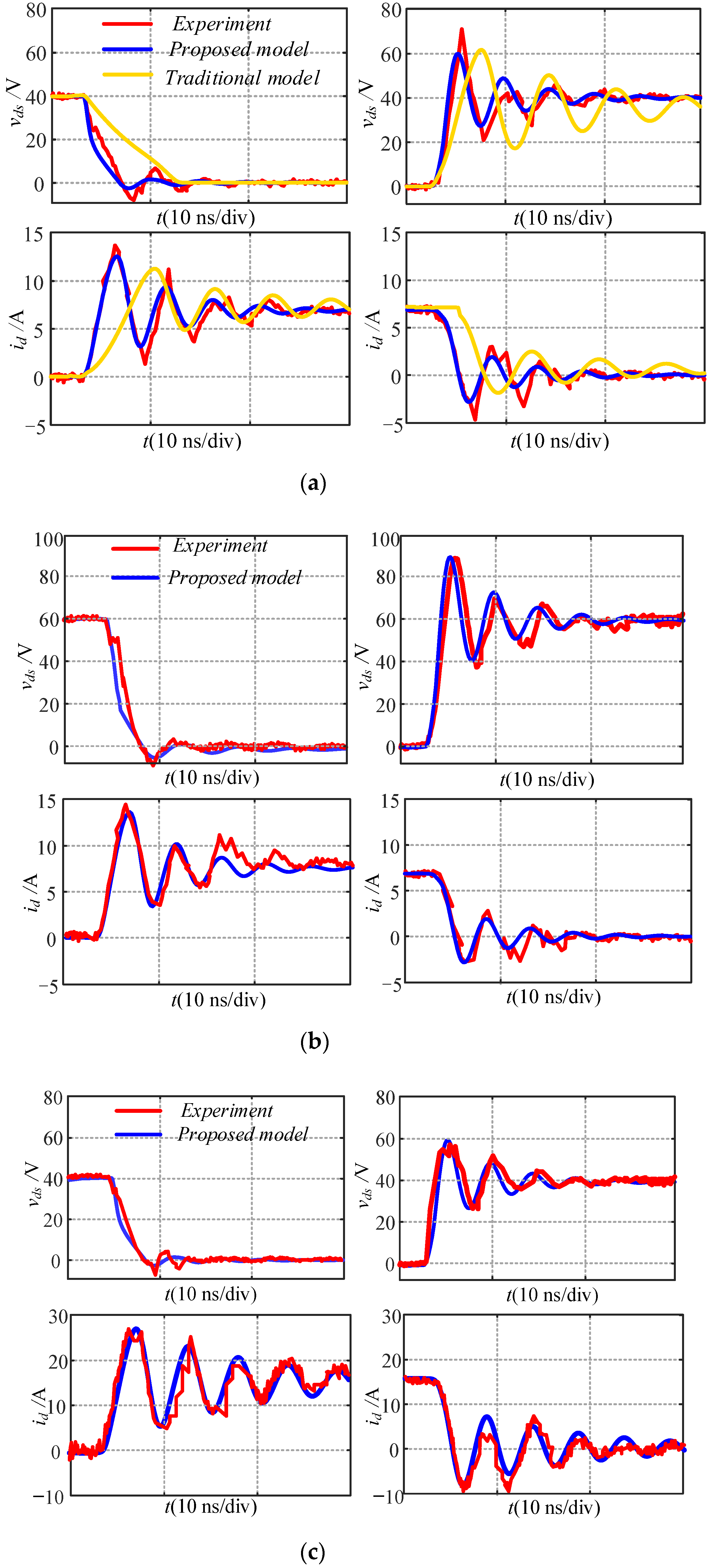
An accurately switching transient analytical model for GaN HEMT considering the influence of nonlinear parameters is proposed in this paper. The analytical derivation of turn-ON process and turn-OFF process is illustrated in detail, and the equivalent circuits are derived for each switching transition. The accuracy of the proposed model is verified by DPT circuit. Experiment results verify that the proposed model is more precise compared with the traditional model. The experimental results show that the maximum relative error of the switching loss can be kept within 10% by the proposed model.
(3)
The effects of gate resistance, gate source capacitance, gate drain capacitance, drain source capacitance, and parasitic inductances on switching characteristic and switching losses are systematically investigated based on the proposed model.

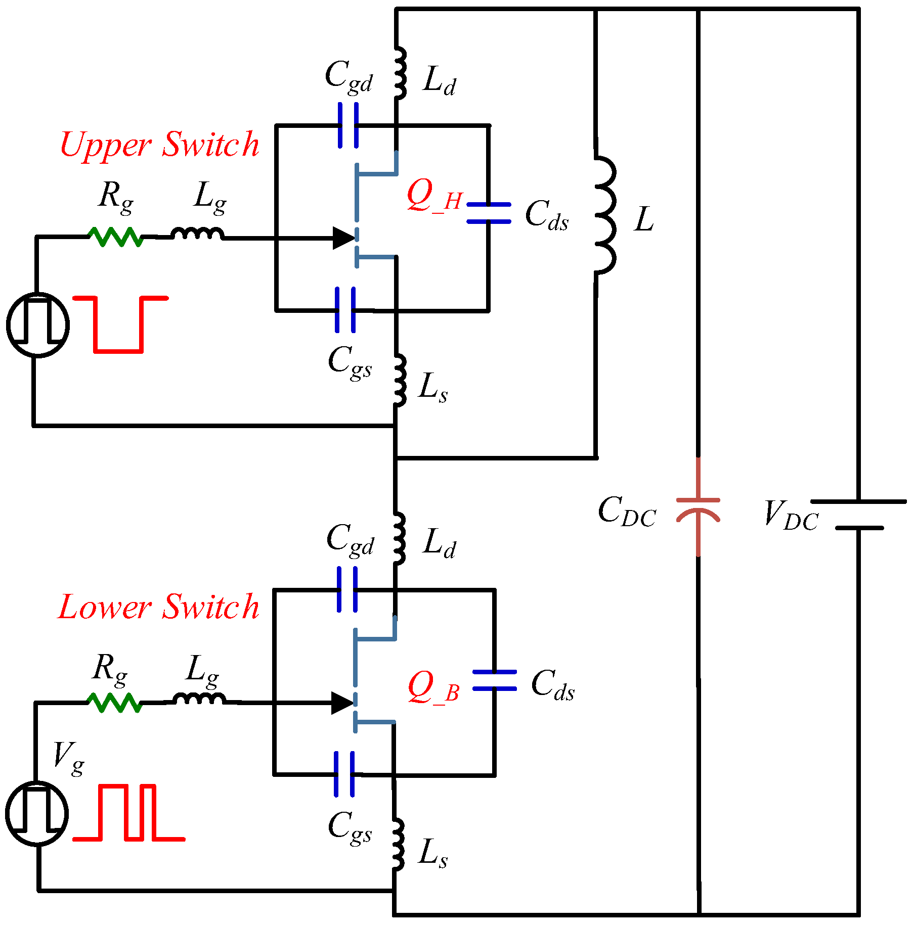
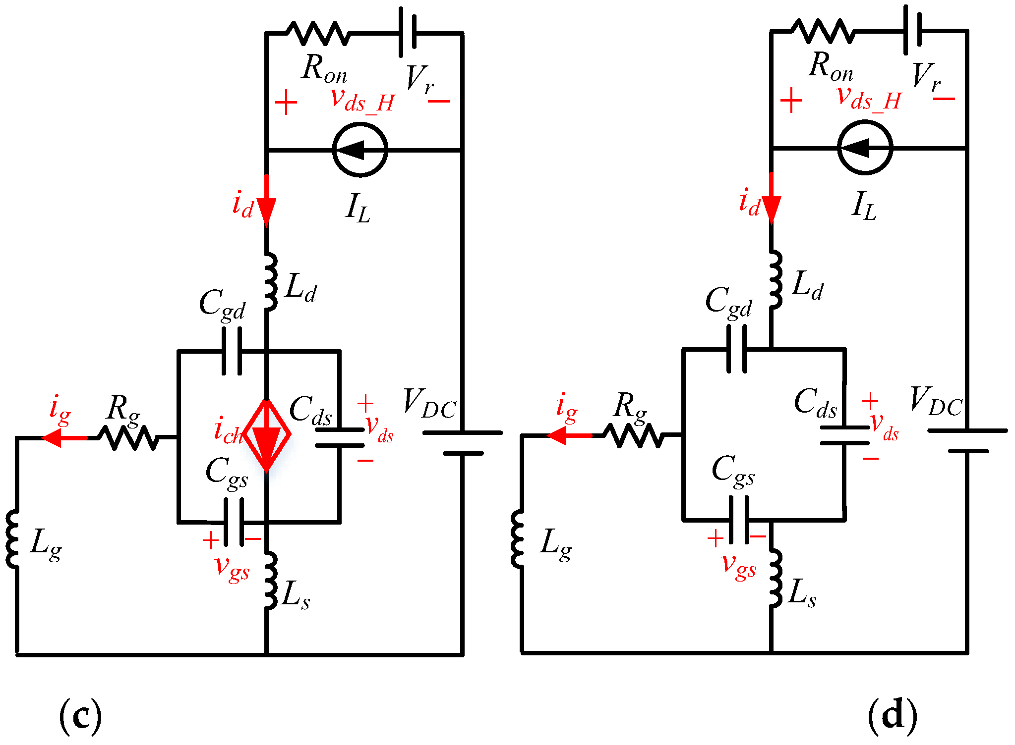
2. Novel Analytical Model of GaN HEMT Device

In order to test and evaluate the switching characteristics of GaN HEMT, a double pulse test (DPT) circuit with inductive load can be adopted as illustrated in Figure 1, where Q and Q_H represent the lower switch and upper GaN HEMT device of the half bridge. In this paper, the GaN HEMT device of GS61004B produced by GaN systems company will be illustrated as an example. Cgs, Cgd, and Cds represent the capacitors of gate source, gate drain, and drain source, respectively. To simplify the circuit analysis, the parasitic inductance and package stray inductance are accounted into Ld, Ls, Lg. Lloop lumps all of the parasitic inductances and package stray inductances along the power loop. The GaN HEMT device does not contain a p-n diode, but the way they conduct in the reverse direction is similar to diodes because this channel is formed by turning on the two-dimensional electron gas (2DEG) in the device.
In Figure 1, it is very important to determine the parasitic inductances and nonlinear parameters to obtain an accurate switching transient analytical model. Generally, the parasitic inductances can be acquired by Maxwell 3-D software and the nonlinear parameters can be obtained by the modeling method, such as the input capacitance Ciss = Cgs + Cgd, the output capacitance Coss = Cds + Cgd, and the reverse capacitance Crss = Cgd. Ciss and Crss can be fitted by simple piecewise linear equation due to their low degree of nonlinearity. However, Coss is a parameter that changes dramatically with the variation of vds at low voltage level, which is with high degree of nonlinearity, and is more difficult to be accurately modeled by the above methods. A nonlinear function tanh(x) will be introduced to represent Coss in this paper, as shown in Equation (1). This function can be used to approximate the Coss during switching process.
tanh ( x ) = e x e x e x + e x
Based on tanh(x), a nonlinear function shown in Equation (2) is proposed to fitting the nonlinear characteristic of the Coss of GS61004B, which can model different changing rate of Coss when vds began to change in low voltage.
C o s s = C o max ( 1 + v d s ( 1 + k 1 ( 1 + tanh ( k 2 v d s + k 3 ) ) ) ) k 4
where Comax, k1, k2, k3, and k4 are the fitting parameters and are given in Table 1. This method has more accuracy modeling results. The modeling results Coss of GaN HEMT is verified in Figure 2a, and it can be concluded that the maximum error between the fitted data and extracted data from the datasheet is less than 3%. Furthermore, this model can also be applied to other different types of devices by adjusting the parameters.
Transconductance gfs describes the dynamic behavioral feature of ich when vgs changes. Using a single value of transconductance has a large opportunity to cause great errors. In this paper, the slope of the tangent line in the transfer characteristic curve is used to approximate the transconductance at the corresponding operation point. Thus, the equation of gfs can be expressed as Equation (3).
{ g f s = 0 v g s < V t h g f s = d i c h d v g s = k 5 ( v g s V t h ) k 6 1 v g s V t h
where k5 and k6 are the fitting parameters which are given in Table 1 as well. Vth is the threshold voltage of gate to source for the device. Figure 2b shows the curve of ich versus vgs. It is obvious that the modeling result makes an accurate estimation based on the proposed model.

3. Transient Characteristic Analysis of Turn-On Process Based on the Proposed Model

A typical waveform during turn-ON process of the GaN HEMT half bridge is shown in Figure 3. There are four stages during the switching process and each stage has different features according to the change of the circuit structure. At each stage, the equations can be obtained from the corresponding equivalent circuit which is illustrated in Figure 4. By solving the equations, we can obtain five variables, namely, the gate current ig, the gate source voltage vgs, the drain current id, the drain source voltage vds, and the drain source voltage vds_H. The nonlinear junction capacitance and nonlinear transconductance modeling results proposed in Section 2 will be applied to the turn-ON process in the following analysis. Thus, the analytical model of each variable during turn-ON process can be derived. Furthermore, the switching loss during the turn-ON process can be obtained.

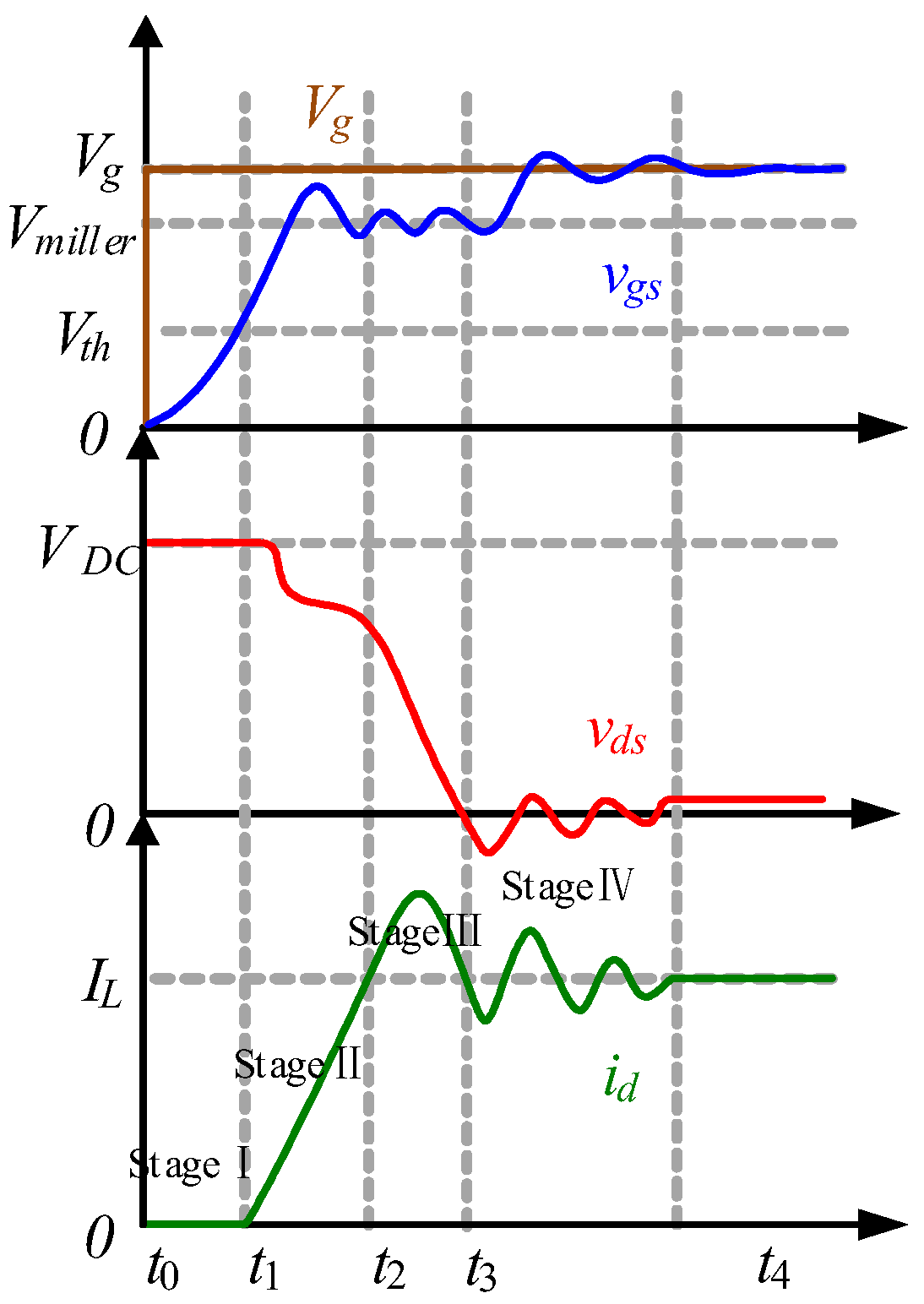
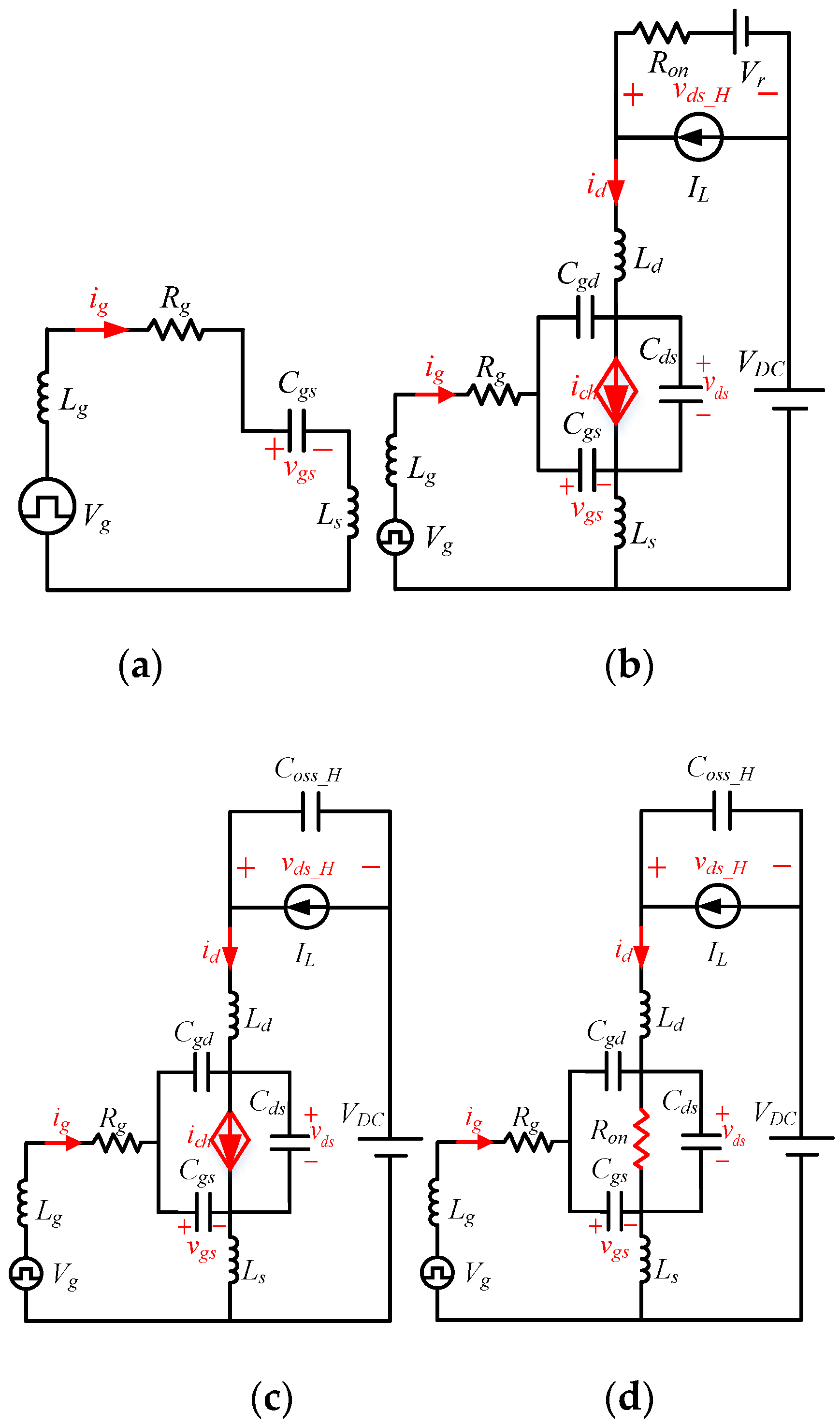
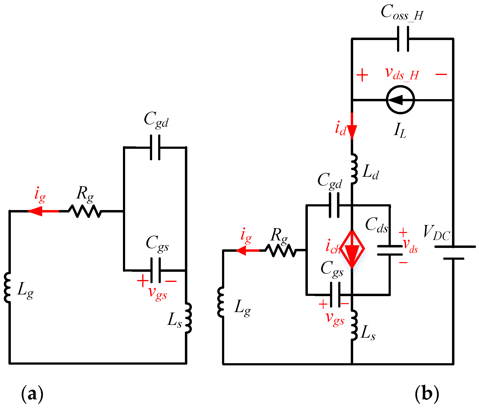
3.1. Stage I (t0–t1): Turn-On Delay Period

As shown in Figure 3, at time t0, the gate drive voltage Vg is applied. In this stage, the gate current charges the capacitance Cgs which causes vgs to rise. The equivalent circuit of this stage is shown in Figure 4a. According to the equivalent circuit, the following equations can be obtained:
V g = ( L g + L s ) d i g d t + R g i g + v g s
i g = C g s d v g s d t
This stage ends at time t1 when vgs reaches the threshold voltage Vth. During this stage, Q is still OFF, the drain source voltage vds, and the drain current id are constant, so there is no switching loss.

3.2. Stage II (t1–t2): Current Rise Period

As shown in Figure 3, at time t1, vgs reaches the threshold voltage Vth, and the channel current ich begins to rise which can be expressed by Equation (3). At the same time, the capacitances Coss begins to discharge through the channel of Q. The drain current id is clamped to the sum of the channel current ich and the Coss discharging current. However, Q_H is still in reverse conduction condition, where Ron is the on-state resistance and Vr represents the reverse conducting voltage drop of Q_H. There will be a voltage drop ΔV between vds and its initial voltage VDC + Vr on the parasitic inductance of the power loop. As shown in the equivalent circuit of Figure 4b, the equations of this stage are as follows:
V g = v g s + R g i g + L g d i g d t + L s ( d i d d t + d i g d t )
i g = C g s d v g s d t + C g d ( d v g s d t d v d s d t )
i d = g f s ( v g s V t h ) + C d s d v d s d t C g d d ( v g s v d s ) d t
V D C = v d s + v d s _ H + ( L d + L s ) d i d d t + L s d i g d t
v d s _ H = R o n ( I L i d ) V r
This stage ends when the drain current id reaches the load current IL. Meanwhile, vgs reaches Miller plateau voltage. It should be especially noted that the voltage drop ΔV is shown in the following equation:
Δ V = ( L d + L s ) d i d d t
In case of Ld and Ls being larger, ΔV will drop faster, so id would change even slower than vds. The transient will skip the voltage drop stage III into ringing stage IV directly. While for small Ld and Ls of properly designed PCB and reasonable current rising speed, stage III will occur as expected.
During this stage, the energy loss can be expressed as:
E o n = t 2 t 1 v d s i c h d t
The power loss in this stage can be determined by:
P o n = f s E o n = f s t 2 t 1 v d s i c h d t
where fs is the switching frequency. However, only id can be measured experimentally, ich cannot. During the turn-ON process, a part of the energy stored in Coss is dissipated through the channel, which is not included in the loss calculated by id. Thus, the relationship can be expressed as:
P o n = f s t 2 t 1 v d s i d d t + P C o s s
where PCoss represents the energy stored in the output capacitance when the applied voltage is VDC + Vr and can be expressed as:
P C o s s = f s 0 V D C + V r v d s C o s s ( v d s ) d v d s
Coss(vds) can be determined by Equation (2), which is plotted in Figure 2a.

3.3. Stage III (t2–t3): Voltage Decline Period

As shown in Figure 3, at time t2, the upper switch GaN HEMT device Q_H stops conducting, and the channel current ich surpasses the load current IL. This surpasses current charge of the output capacitance Coss_H of Q_H. The upper switch can be equivalent to the output capacitor Coss_H, and vds_H is increased. Correspondingly, vds decreases and Coss continues to discharge through the channel of Q. id may have a ringing because of the effect of parasitic LC elements on the device. The equivalent circuit of this stage is illustrated in Figure 4c. The circuit equations can be expressed as:
i d = g f s ( v g s V t h ) + C d s d v d s d t C g d d ( v g s v d s ) d t
V g = v g s + R g i g + L g d i g d t + L s ( d i d d t + d i g d t )
i g = C g s d v g s d t + C g d ( d v g s d t d v d s d t )
V D C = v d s + v d s _ H + ( L d + L s ) d i d d t + L s d i g d t
i d = I L + C o s s _ H d v d s _ H d t
This period ends when vds decreases to zero. A current overshoot is caused by the rapid dv/dt action on the output capacitance:
Δ i d = C o s s _ H d v d s _ H d t C o s s d v d s d t
In addition, the Miller plateau time on vgs for GaN HEMT is less than Si MOSFET because of small transfer capacitance Cgd. This characteristic can help us to understand why GaN HEMT can turn-ON at a high speed. The turn-ON switching loss calculation method is the same as that of Equation (15).

3.4. Stage IV (t3–t4): Ringing Period

As shown in Figure 3, at time t3, Q will work in the linear region and behave equivalent to a loop resistor, as illustrated in Figure 4d. Usually, the ringing is serious due to small damping resistance with large parasitic inductances. The key equations can be expressed as:
V g = v g s + R g i g + L g d i g d t + L s ( d i d d t + d i g d t )
i g = C g s d v g s d t + C g d ( d v g s d t d v d s d t )
V D C = v d s + v d s _ H + ( L d + L s ) d i d d t + L s d i g d t
i d = v d s R o n + C d s d v d s d t C g d d ( v g s v d s ) d t
i d = I L + C o s s _ H d v d s _ H d t
where Ron represents the on-state resistance of Q. During this stage, the turn-ON switching loss can be expressed as:
P o n = f s t 4 t 3 ( i d I L ) 2 R o n d t
This period ends when the ringing is fully damped.

4. Transient Characteristic Analysis of Turn-Off Process Based on the Proposed Model

There are still four stages and the typical waveforms during turn-OFF process. At each stage, the equations can be obtained from each equivalent circuit. Similarly, the nonlinear junction capacitance and nonlinear transconductance modeling results proposed in Section 2 are applied to the turn-OFF process and five state variables can be calculated according to the equations obtained from the equivalent circuit of each stage. Furthermore, the switching loss during the turn-OFF process can be obtained. The calculation of each stage will be discussed as follows.

4.1. Stage I (t5–t6): Turn-Off Delay Period

As shown in Figure 5, at time t5, the gate drive voltage Vg declines to 0 V. In this stage, Cgs and Cgd are discharged, so vgs begins to reduce. However, Q is still in the turn-ON state, IL keeps flowing through the channel of Q. The equivalent circuit of this stage is shown in Figure 6a. The following equations can be obtained:
0 = ( L g + L s ) d i g d t + R g i g + v g s
i g = ( C g s + C g d ) d v g s d t
This period ends at time t6 when vgs reaches the Miller plateau voltage vmiller.
v m i l l e r = V t h + I L g f s
vds and id are constants, so there is no turn-OFF switching loss in this stage.

4.2. Stage II (t6–t7): Voltage Rise Period

As shown in Figure 5, at time t6, the channel of Q starts to turn-OFF, so the channel current ich decreases and begins to charge the capacitances Cds and Cgd, then vds is rapidly increased. At the same time, Coss_H begins to discharge, resulting in the decline of vds_H. However, Q_H is still not reverse conducting because id is limited by the power loop parasitic inductances. Therefore, the decrease rate of id is smaller than that of ich. The equivalent circuit is shown in Figure 6b, and the equations of this stage are as follows:
0 = v g s + R g i g + L g d i g d t + L s ( d i d d t + d i g d t )
i g = C g s d v g s d t + C g d ( d v g s d t d v d s d t )
i d = g f s ( v g s V t h ) + C d s d v d s d t C g d d ( v g s v d s ) d t
V D C = v d s + v d s _ H + ( L d + L s ) d i d d t
i d = I L + C o s s _ H d v d s _ H d t
This period ends when vds_H reaches −Vr. During this stage, the energy loss can be calculated as:
E o f f = t 7 t 6 v d s i c h d t
The power loss in this stage can be determined by:
P o f f = f s E o f f = f s t 7 t 6 v d s i c h d t
Usually, the energy stored in Coss is quite large due to the high peak vds. The power loss is different from turn-ON process because id contains the charge current from Coss. Thus, the relationship can be modified as:
P o f f = f s t 7 t 6 v d s i d d t P C o s s
where PCoss is the energy stored in Coss when the applied voltage is vPeak and can be calculated as:
P C o s s = f s 0 v p e a k v d s C o s s ( v d s ) d v d s
Coss(vds) can be determined by Equation (2) and is plotted in Figure 2a.

4.3. Stage III (t7–t8): Current Decline Period

As shown in Figure 5, at time t7, Q_H starts to reverse conduct. During this stage, id and vgs decreases, vds continues to increase, and Cds and Cgd are charged. The equivalent circuit is shown in Figure 6c, and the circuit equations can be expressed as:
0 = v g s + R g i g + L g d i g d t + L s ( d i d d t + d i g d t )
i g = C g s d v g s d t + C g d ( d v g s d t d v d s d t )
i d = g f s ( v g s V t h ) + C d s d v d s d t C g d d ( v g s v d s ) d t
V D C = v d s + v d s _ H + ( L d + L s ) d i d d t + L s d i g d t
v d s _ H = R o n ( I L i d ) V r
This stage ends when id drops to zero. The turn-OFF power loss calculation method is the same as Stage II.

4.4. Stage IV (t8–t9): Ringing Period

As shown in Figure 5, at time t8, when vgs drops below Vth, the channel of Q is totally shut down. Then vgs continues to decrease until it reaches zero. During this stage, vds and id both have a ringing due to the oscillation between the parasitic inductances and Coss. The equivalent circuit is shown in Figure 6d, and the circuit equations can be expressed as:
0 = v g s + R g i g + L g d i g d t + L s ( d i d d t + d i g d t )
i g = C g s d v g s d t + C g d ( d v g s d t d v d s d t )
i d = C d s d v d s d t C g d d ( v g s v d s ) d t
V D C + V r = v d s + ( L d + L s ) d i d d t
During this stage, the turn-OFF power loss calculation method can be expressed as:
P o f f = f s t 9 t 8 i d v d s d t
This period ends when the ringing is fully damped.

5. Experimental Verifications

In order to verify the accuracy of the proposed switching transient analytical model, a DPT experiment prototype was built, as shown in Figure 7. The double pulses will be applied to the gate of the bottom GaN HEMT by TMS320F28335. The device under test is the GS61004B 100 V enhanced GaN HEMT and the driver is Si8271. The oscilloscope is MDPO3054 by Tektronix Inc. The switching current is measured with 2000 MHz bandwidth current shunt SSDN-10 by T&M Research Products Inc. The parasitic inductance and package stray inductance can be acquired by Maxwell 3-D. The specifications and the main circuit parameters are shown in Table 2. The comparisons among the switching waveforms provided by the experiment, the proposed model, and the traditional mode in [16] are shown in Figure 8. The calculated results from the models for the variables vds and id with fitting value from Figure 2 will be used to evaluate the model accuracy. The loss calculation results are shown in Figure 9.
It can be concluded that the proposed model matches more accurately with the experimental results than the traditional model according to the slope and spike of id and vds from Figure 8. The oscillation frequency and amplitude of the waveforms from the experimental results deviate from the traditional model while the proposed model results agree with that accurately. The reason is that the traditional model treats the nonlinear parameters in the device as fixed values.
Subsequently, the energy loss of Eon and Eoff is calculated by the proposed loss calculation method as shown in Figure 9. The results show that the energy loss increases when the load current changes from 5 A to 10 A. It is obvious that the loss calculation results of the proposed model in this paper are more precise compared with the traditional model. Experiment results verify the accuracy of the proposed loss calculation method with a maximum relative error of less than 10%. Finally, it can be concluded that the proposed switching transient analytical model is quite accurate and the loss analysis results based on the model is believable.

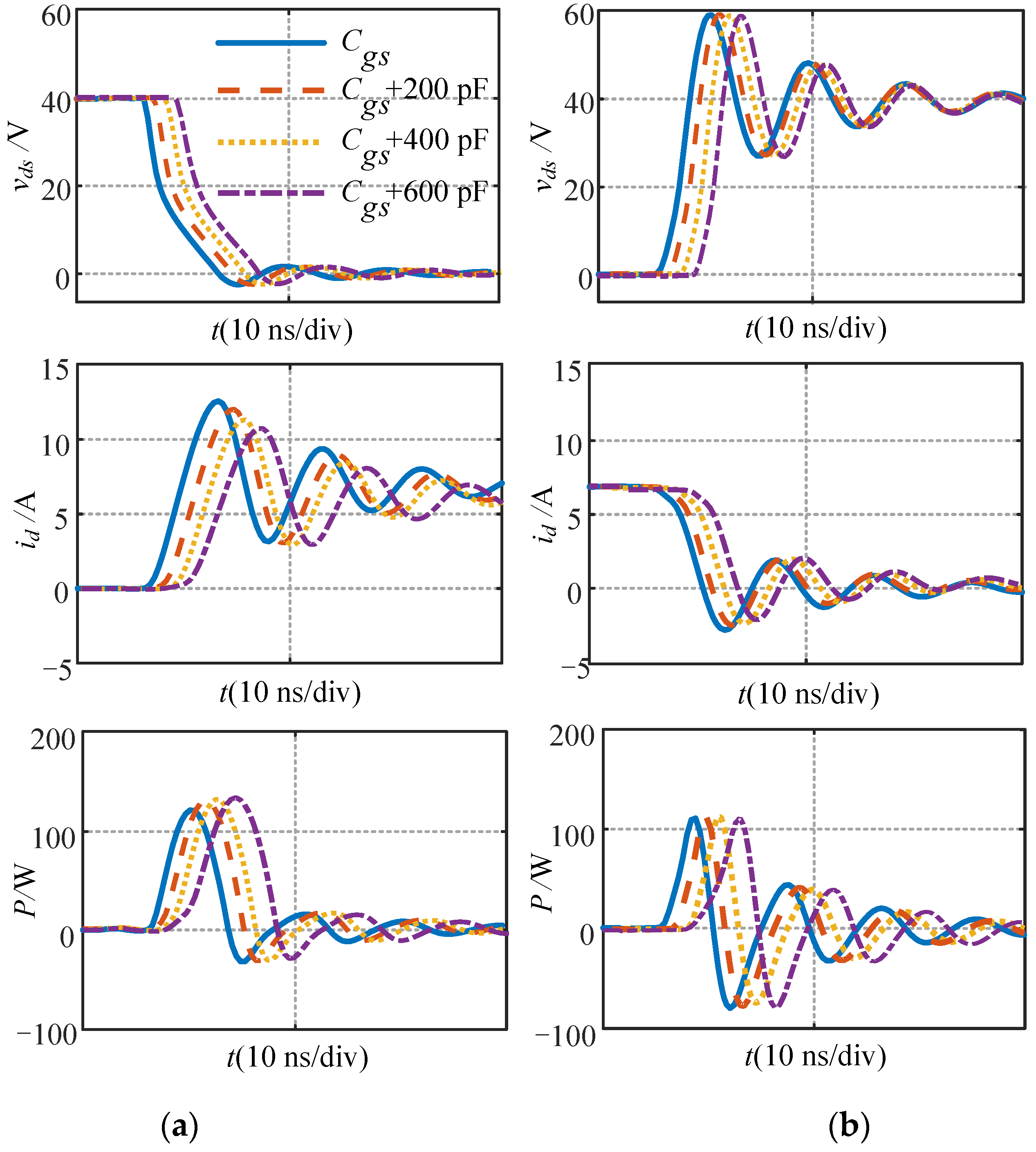
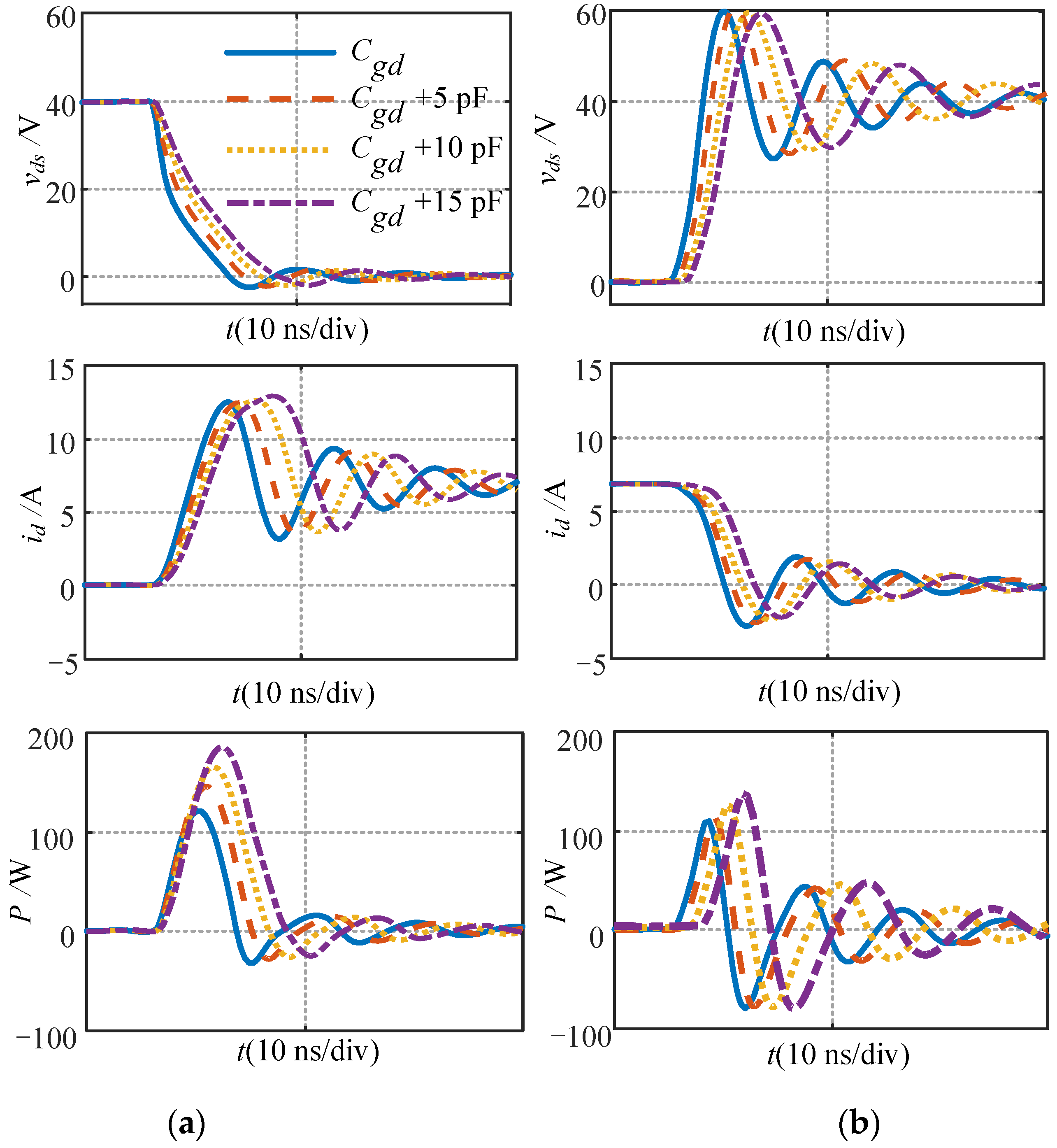
6. Effect of Parameter Variation on the Analytical Model

The effectiveness of the proposed switching transient analytical model is verified in the previous section. Moreover, it is important to evaluate how the gate resistance Rg, the nonlinear junction capacitances Cgs, Cgd, Cds, and the parasitic inductance Lloop affect the switching transient and switching loss, thus the further improvement of packaging and application of the device can be inspired.
Figure 10 shows the effect of different driving resistors Rg on the switching transition behavior. The waveforms of vds and id are plotted. It can be seen that the oscillation of vds and id can be effectively suppressed by increasing the Rg. However, the larger Rg limits the gate charging current and reduces the charging speed, thus resulting the switching time increase of the device. In addition, Figure 10 also calculates the influence of different Rg on switching loss. With the increase of Rg, the turn-ON and turn-OFF switching loss is also increased. However, with the increase of Rg, the current overshoot for turn-ON transient and the voltage overshoot for turn-OFF transient decreased. Therefore, considering the impact of switching loss and overshoot in practical application, it is necessary to select an appropriate Rg value.
In order to simplify the analysis, Lloop lumps all of the parasitic inductances and package stray inductances along the power loop. As the package stray inductances are accounted into Ld and Ls, so Lloop is the sum of Ld and Ls. The effect of different Lloop on the switching transition behavior is shown in Figure 11. During the turn-ON process, the change rate of id and vds become slower with the increase of Lloop. Meanwhile, the current overshoot decreases but the voltage overshoot increases. In addition, the ringing period of id and vds becomes larger. These factors cause the turn-ON switching loss to become larger due to overlap area increases. During the turn-OFF process, the increase of Lloop has an obvious influence on id overshoot, which also leads to the increase of loss. It can be concluded that the total loss also increases, therefore, the value of Lloop should be minimized as much as possible on the PCB design and optimization process.
For the same type of GaN HEMT, the value of the nonlinear junction capacitances should be the same. However, due to different production processes or different production lines, the capacitance values may change. In order to explore the effect of the nonlinear junction capacitance on the switching transient, we make corresponding changes for each nonlinear junction capacitance value within a reasonable range.
The influence of Cgs is shown in Figure 12. Set the variation value of Cgs as 200 pF, 400 pF, 600 pF. It is observed that the increasing of Cgs caused the charge time to become longer, thus resulting in the turn-ON delay time notably increasing. Meanwhile, the current overshoot and the voltage overshoot during the turn-OFF process can be suppressed by increasing Cgs. In general, Cgs can effectively reduce the waveform oscillation, but will also lead to an increase in switching loss. Therefore, an extra capacitor paralleled with Cgs can be used to reduce the oscillation when the oscillation is too large. However, the value of the parallel capacitor should be selected properly, otherwise the loss will be too large.
The effect of Cgd is shown in Figure 13. As stated previously, the increase of Cgd has a large effect on the switching loss model. It can be concluded that the magnitude of Cgd mainly affects the turn-ON process, i.e., the change rate of id and vds decreases and the conducting time increases. Although the increase of Cgd is only 5 pF–15 pF, it has a great impact on the on-off time and switching loss due to the capacitor which affects the length of Miller platform time. Therefore, Cgd should be designed as small as possible in device production. Compared with the Si devices, GaN HEMT is able to achieve much faster switching speeds and lower switching losses due to its smaller Cgd.
The influence of Cds is shown in Figure 14. As we know, Coss is a nonlinear junction capacitance of vds. It can be concluded that the increase of Cds mainly affects the change rate of id. Since Coss increases with the increase of Cds, according to Equation (17), the energy stored in Coss will increase, which will result in an increase in the switching loss. In addition, the switching speed is increased and the ringing period becomes larger. For the convenience of overall consideration, the influencing parameter of switching characteristics and their specific impact analysis are listed in Table 3.

7. Conclusions

In this paper, an accurate switching transient analytical model for GaN HEMT under the influence of nonlinear parameters was proposed. The proposed model covers the process of turn-ON and turn-OFF, which is of great significance in understanding the dynamic characteristics during the switching process. In addition, this model can be applied to evaluate the influence of parameter changes on the switching characteristics of devices, and calculate the switching loss. Finally, the following conclusions can be drawn:
(1)
Switching speed. The switching process of the GaN HENT are essentially the charging process of its nonlinear junction capacitances. With the increases of Cgs, Cgd, Cds, Lloop and Rg, the switching speed is slowed down. Since the channel current is gate-source voltage dependent in the saturation region, it is out of the question that Cgs can affect the current slew rate. As for the voltage slew rate, it is clarified that the charging of Cgd leads to the change in the drain source voltage. The loop parasitic inductances Lloop and gate resistance Rg decrease the change rate of id and vds with the increase of Lloop and Rg.
(2)
Current and voltage overshoot. The current and voltage overshoot in switching transient can be suppressed by increasing Rg. The current overshoot can be suppressed by increasing Cgs. The current and voltage overshoot can be worsened by increasing Lloop. The current overshoot can be worsened by increasing Cds. Cgd cannot affect the current and voltage overshoot.
(3)
Switching loss. Both Cgs, Cgd, Cds, Lloop and Rg increases switching loss by slowing down the switching speed and prolonging the switching process.
(4)
Design guidelines. It can be concluded that parameter changes of the GaN HEMT have a profound influence on the switching performance; hence, it calls for special attention to the selection of components and circuit design. The voltage change rate is most sensitive to Cgd, Lloop and Rg; for high-speed high-voltage applications, these values should not be large. The current change rate is most sensitive to Cgs, Cds, Lloop, and Rg. Therefore, the PCB traces should be carefully routed to reduce the stray inductance in the circuit. The other parasitic elements should be minimized to achieve fast switching and low loss.

Author Contributions

All authors contributed to the writing and revisions; writing—review and editing, L.H.; writing—original draft, D.Y.; review, Y.H.; review, Z.H.; supervision, P.Z. All authors have read and agreed to the published version of the manuscript.

Funding

This research was funded by the National Natural Science Foundation of China, grant numbers 51777049, 51707051.

Institutional Review Board Statement

Not applicable.

Informed Consent Statement

Not applicable.

Data Availability Statement

Data available on request due to privacy or ethical restrictions.

Conflicts of Interest

The authors declare no conflict of interest.

References

  1. Afonso, J.L.; Tanta, M.; Pinto, J.G.O.; Monteiro, L.F.C.; Machado, L.; Sousa, T.J.C.; Monteiro, V. A Review on Power Electronics Technologies for Power Quality Improvement. Energies 2021, 14, 8585. [Google Scholar] [CrossRef]
  2. Maddi, H.L.R.; Yu, S.; Zhu, S.; Liu, T.; Shi, L.; Kang, M.; Xing, D.; Nayak, S.; White, M.H.; Agarwal, A.K. The Road to a Robust and Affordable SiC Power MOSFET Technology. Energies 2021, 14, 8283. [Google Scholar] [CrossRef]
  3. Ramachandran, R.; Nymand, M. Experimental demonstration of a 98.8% efficient isolated DC–DC GaN converter. IEEE Trans. Ind. Electron. 2017, 64, 9104–9113. [Google Scholar] [CrossRef]
  4. Ren, Y.C.; Xu, M.; Zhou, J.H.; Lee, F.C. Analytical loss model of power MOSFET. IEEE Trans. Power Electron. 2006, 21, 310–319. [Google Scholar]
  5. Xiong, Y.; Sun, S.; Jia, H.; Shea, P. New physical insights on power MOSFET switching losses. IEEE Trans. Power Electron. 2009, 24, 525–531. [Google Scholar] [CrossRef]
  6. Wang, J.; Chung, H.S.; Li, R.T. Characterization and experimental assessment of the effects of parasitic elements on the MOSFET switching performance. IEEE Trans. Power Electron. 2013, 28, 573–590. [Google Scholar] [CrossRef]
  7. Turzynski, M.; Kulesza, W.J. A simplified behavioral MOSFET model based on parameters extraction for circuit simulations. IEEE Trans. Power Electron. 2016, 31, 3096–3105. [Google Scholar] [CrossRef]
  8. Christen, D.; Biela, J. Analytical switching loss modeling based on datasheet parameters for MOSFET in a Half-bridge. IEEE Trans. Power Electron. 2019, 34, 3700–3710. [Google Scholar] [CrossRef]
  9. Costinett, D.; Maksimovic, D.; Zane, R. Circuit-oriented treatment of nonlinear capacitances in switched mode power supplies. IEEE Trans. Power Electron. 2015, 30, 985–995. [Google Scholar] [CrossRef]
  10. Sakairi, H.; Yanagi, T.; Otake, H.; Kuroda, N.; Tanigawa, H. Measurement methodology for accurate modeling of SiC MOSFET switching behavior over wide voltage and current ranges. IEEE Trans. Power Electron. 2018, 33, 7314–7325. [Google Scholar] [CrossRef]
  11. Roy, S.K.; Basu, K. Analytical estimation of turn ON switching loss of SiC MOSFET and schottky diode pair from datasheet parameters. IEEE Trans. Power Electron. 2019, 34, 9118–9130. [Google Scholar] [CrossRef]
  12. Sun, J.; Yuan, L.; Duan, R.; Lu, Z.; Zhao, Z. A semi-physical semi-behavioral analytical model for switching transient of SiC MOSFET module. IEEE J. Emerg. Sel. Top. Power Electron. 2021, 9, 2258–2270. [Google Scholar] [CrossRef]
  13. Chen, K.; Zhao, Z.; Yuan, L.; Lu, T.; He, F. The impact of nonlinear junction capacitance on switching transient and its modeling for SiC MOSFET. IEEE Trans. Electron Device 2014, 62, 333–338. [Google Scholar] [CrossRef]
  14. Wang, X.; Zhao, Z.; Li, K.; Zhu, Y.; Chen, K. Analytical methodology for loss calculation of SiC MOSFETs. IEEE J. Emerg. Sel. Top. Power Electron. 2018, 7, 71–83. [Google Scholar] [CrossRef]
  15. Xie, R.; Wang, H.; Tang, G.; Yang, X.; Chen, K.J. An analytical model for false turn-on evaluation of high-voltage enhancement-mode GaN transistor in bridge-leg configuration. IEEE Trans. Power Electron. 2017, 32, 6416–6433. [Google Scholar] [CrossRef]
  16. Wang, K.; Yang, X.; Li, H.; Ma, H.; Zeng, X.; Chen, W. An Analytical Switching Process Model of Low-Voltage eGaN HEMTs for Loss Calculation. IEEE Trans. Power Electron. 2016, 31, 635–647. [Google Scholar] [CrossRef]
  17. Chen, J.; Luo, Q.; Huang, J.; He, Q.; Du, X. A Complete Switching Analytical Model of Low-Voltage eGaN HEMTs and Its Application in Loss Analysis. IEEE Trans. Ind. Electron. 2020, 67, 1615–1625. [Google Scholar] [CrossRef]
  18. Kozak, J.P.; Barchowsky, A.; Hontz, M.R.; Koganti, N.B.; Stachina, W.H.; Reed, G.F.; Mao, Z.; Khana, R. An Analytical Model for Predicting Turn-ON Overshoot in Normally-OFF GaN HEMTs. IEEE J. Emerg. Sel. Top. Power Electron. 2020, 8, 99–110. [Google Scholar] [CrossRef]
  19. Xin, Y.; Chen, W.; Sun, R.; Shi, Y.; Zhang, B. Analytical Switching Loss Model for GaN-Based Control Switch and Synchronous Rectifier in Low-Voltage Buck Converters. IEEE J. Emerg. Sel. Top. Power Electron. 2019, 7, 1485–1495. [Google Scholar] [CrossRef]
  20. Long, X.; Liang, W.; Jun, Z.; Chen, G. A Normalized Quantitative Method for GaN HEMT Turn-ON Overvoltage Modeling and Suppressing. IEEE Trans. Power Electron. 2019, 66, 2766–2775. [Google Scholar] [CrossRef]
  21. Huang, X.; Li, Q.; Liu, Z.; Lee, F.C. Analytical Loss Model of High Voltage GaN HEMT in Cascode Configuration. IEEE Trans. Power Electron. 2014, 29, 2208–2219. [Google Scholar] [CrossRef]
  22. Li, Q.; Liu, B.; Duan, S. Simplified analytical model for estimation of switching loss of cascode GaN HEMTs in totem-pole PFC converters. Chin. J. Electr. Eng. 2019, 5, 1–9. [Google Scholar] [CrossRef]
Figure 1. Circuit schematic of double pulse test bench.
Energies 15 02966 g001
Figure 2. Modeling results and datasheet: (a) Nonlinear capacitances; (b) Transfer characteristic curves.
Energies 15 02966 g002
Figure 3. Typical waveforms during turn-ON process.
Energies 15 02966 g003
Figure 4. Equivalent circuits for different stages during turn-ON period: (a) Stage I; (b) Stage II; (c) Stage III; (d) Stage IV.
Energies 15 02966 g004
Figure 5. Typical waveforms during turn-OFF process.
Energies 15 02966 g005
Figure 6. Equivalent circuits for different stages during turn-OFF process: (a) Stage I; (b) Stage II; (c) Stage III; (d) Stage IV.
Energies 15 02966 g006aEnergies 15 02966 g006b
Figure 7. Experiment circuit prototype.
Energies 15 02966 g007
Figure 8. Switching waveforms of the experiment, the proposed model, and the traditional model: (a) VDC = 40 V, IL = 7 A; (b) VDC = 60 V, IL = 7 A; (c) VDC = 40 V, IL = 15 A.
Energies 15 02966 g008
Figure 9. Switching loss of the experiment, the proposed model, and the traditional model: (a) turn-ON energy loss; (b) turn-OFF energy loss.
Energies 15 02966 g009
Figure 10. Influence of different Rg on the switching transient: (a) turn-ON process; (b) turn-OFF process.
Energies 15 02966 g010
Figure 11. Influence of different Lloop on the switching transient: (a) turn-ON process; (b) turn-OFF process.
Energies 15 02966 g011
Figure 12. Influence of different Cgs on the switching transient: (a) turn-ON process; (b) turn-OFF process.
Energies 15 02966 g012
Figure 13. Influence of different Cgd on the switching transient: (a) turn-ON process; (b) turn-OFF process.
Energies 15 02966 g013
Figure 14. Influence of different Cds on the switching transient: (a) turn-ON process; (b) turn-OFF process.
Energies 15 02966 g014
Table 1. Fitting parameters.
SymbolValue
Comax311 pF
k1−0.456
k2−0.51
k39.5
k4−0.256
k530
k60.75
Table 2. Specifications and main circuit parameters.
ParametersValue
VDC40 V
IL7 A
Ron0.57 Ω
Ls5.6 nH
Ld3.7 nH
Lg2.8 nH
Rg10 Ω
Vg6 V
Table 3. Analysis of The Influencing Parameter of Switching Characteristics.
ParametersTurn-On Switching SpeedTurn-Off Switching SpeedTurn-On
Current Overshoot
Turn-Off Voltage OvershootTurn-Off Current
Overshoot
Turn-On LossTurn-Off Loss
RgIncreaseIncreaseDecreaseDecreaseDecreaseIncreaseIncrease
LloopIncreaseIncreaseDecreaseInvariantIncreaseIncreaseIncrease
CgsIncreaseIncreaseDecreaseInvariantDecreaseIncreaseIncrease
CgdIncreaseIncreaseIncreaseInvariantInvariantIncreaseIncrease
CdsInvariantIncreaseInvariantInvariantIncreaseInvariantIncrease
Publisher’s Note: MDPI stays neutral with regard to jurisdictional claims in published maps and institutional affiliations.

