Article

A Single-Phase Transformerless Nine-Level Inverter and Its Control Strategy

1
School of Electronic and Electrical Engineering, Shangqiu Normal University, Shangqiu 476000, China
2
School of Electrical Engineering and Automation, Anhui University, Hefei 230601, China
3
School of Electrical Engineering, Shandong University, Jinan 250061, China
4
National Engineering Laboratory of Efficiency-Saving Motor & Control Technology, Heifei 230601, China
*
Author to whom correspondence should be addressed.
Energies 2022, 15(9), 3418; https://doi.org/10.3390/en15093418
Submission received: 28 March 2022 / Revised: 25 April 2022 / Accepted: 5 May 2022 / Published: 7 May 2022
(This article belongs to the Special Issue Energy, Electrical and Power Engineering 2021-2022)

Abstract

:
To reduce the device number per unit level of the existing nine-level inverters, a topology of single-phase transformerless nine-level inverter was proposed. The proposed topology consists of only 10 switching devices and 4 capacitors. Firstly, the working principle of the proposed topology was analyzed in detail, and the comparison with conventional nine-level topologies in terms of device switching loss and conduction loss was presented. Then, combined with one-dimensional space vector modulation, a floating capacitor voltage estimation method was presented by the analysis of the operation mode before the arrival of redundant switching state. On this basis, a floating capacitor voltage sensorless control scheme was proposed, to achieve the balance of the floating capacitor voltages. Finally, simulations and experiments verified the effectiveness and correctness of the proposed topology and floating capacitor voltage sensorless control method.

1. Introduction

In recent years, high-order multi-level inverters have attracted the attention of many scholars in low-voltage applications such as new energy power generation, microgrids, and motor drives, due to their advantages of high output power quality, low current harmonics, and low voltage stress of switching devices [1,2,3,4,5]. At present, multi-level inverter circuits mainly include neutral-point-clamped (NPC), flying capacitors (FC), cascaded H-bridge (CHB), stacked multicell converter (SMC) and other topologies. A nine-level active NPC (ANPC) inverter topology is proposed to expand the inverter capacity while reducing the filter size by interleaving and paralleling two five-level ANPC inverters [6]. However, this topology requires 24 switching devices, and the circuit hardware cost is high. A new approach is developed in [7], which connects four flying capacitor H-bridges in series with one two-level half bridge, effectively reducing the number of switching devices in the nine-level topology to 18, but the flying capacitor voltage control of this topology is relatively complex. The nine-level inverter topology presented in [8] uses a switched capacitor circuit combined with an H-bridge. This circuit only needs one voltage source, and fewer switching devices. Although the voltage stress of switching devices is relatively small, the energy of this circuit can only be transmitted in one direction. The stacked multi-unit multi-level circuit is proposed in [9,10], which not only reduces the energy storage of the inverter, but also improves the voltage withstand capability of the circuit. The above-mentioned multi-level topology is not suitable for low-voltage application, due to the large number of devices and complex control. In order to solve the above problems, four nine-level topologies suitable for low-voltage application are proposed in the literature [11,12,13]. However, these topologies require more DC power sources in practical applications, which greatly increases the system cost.
The unbalance of floating capacitor voltages has always been one of the key problems to be solved in high-order multilevel inverters. Thus, several floating capacitor voltage balance control methods have been proposed. A capacitance voltage estimation method is proposed in [14]. By connecting a voltage sensor between two capacitor anodes and analyzing the current flow path, only half of the voltage sensors can estimate the overall capacitance voltage. The SVPWM modulation strategy is adopted in [15,16], and the balance between the dc-link capacitor voltages and the floating capacitor voltages is achieved by reasonably selecting the redundant vector. However, due to the large number of voltage vectors, the calculation is very complicated. Compared with the SVPWM method, the SPWM is simple and has been widely used in high-order multi-level topologies. A simple logic-form equation based PWM is designed in [17], which can make the floating capacitors voltage around its reference value. An inverter capacitor voltage balancing method based on optimal zero sequence voltage injection is proposed in [18]. This method is realized by hybrid carrier pulse width modulation, which can balance and adjust the voltage of DC link capacitor and floating capacitors in the topology. A new carrier-based modulation scheme was adopted in [19], which solves the problem of floating capacitors voltage balance by clamping the modulation reference safely to the pole voltage level conducive to floating capacitors voltage balance. A SPWM-based floating capacitor voltage control method is proposed in [20], which achieves the balance of the floating capacitor voltage by reasonably selecting redundant switch states during phase switching. By adjusting the duty cycle, the dwell time of the redundant switch state is changed, and then the floating capacitor voltages are controlled to be balanced [21]. A one-dimensional space vector modulation method is proposed in [22], which can achieve the voltage balance of the floating capacitors while reducing the switching loss and the control complexity. Compared with SPWM, the one-dimensional space vector can increase the control degree of freedom of the inverter, which is more conducive to the high-frequency output of the inverter.
However, the realization of the above-mentioned floating capacitor voltage balance methods requires the use of voltage sensor to obtain a voltage signal. Since the actual operating environment of the inverter is complex, humidity, vibration, noise, electromagnetic interference, etc. will affect the measurement accuracy of the sensor, and even lead to sensor failure. Therefore, how to realize sensorless control or less sensor control is the key to ensure the reliable operation of the inverter system. However, most of the existing sensorless control strategies are proposed to cancel the grid voltage or current sensors [23,24,25], while the floating capacitor voltage sensorless control is relatively rarely reported.
To tackle the above problems, this paper proposes a low-voltage single-phase non-isolated nine-level inverter topology with simple structure and few switching devices, and it presents a floating capacitor voltage sensorless control strategy based on one-dimensional space vector modulation. First, the working principle of the proposed nine-level inverter is analyzed in detail, and the comparison with the existing nine-level topologies is presented. Then, combined with the one-dimensional space vector modulation algorithm, a control strategy without floating capacitor voltage sensor is proposed, and the voltage balance is realized by estimating and predicting the floating capacitor voltages. Finally, simulation and experimental results have verified the validity and feasibility of the proposed topology and control algorithm.

2. The Proposed Nine-Level Inverter Topology and Its Working Principle
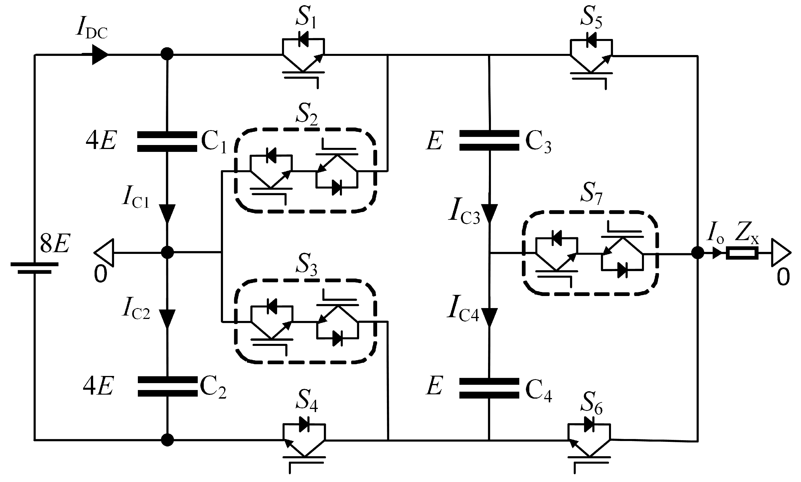
2.1. Topology

The proposed single-phase non-isolated nine-level inverter topology is shown in Figure 1. The circuit is mainly composed of 10 switching devices and 4 capacitors. S2, S3, and S7 are composed of two switching devices, which are bidirectional blocking switches, and S1, S4, S5 and S6 are unidirectional blocking switches. Assuming that the total dc-link voltage VDC is 8E, the voltage of the dc-link capacitors C1 and C2 is 4E, and the voltage of the floating capacitors C3 and C4 is E. IDC and IO are the dc-link current and load current, respectively, while IC1, IC2, IC3 and IC4 are the currents flowing through the capacitors C1, C2, C3 and C4, respectively.

2.2. Working Modal Analysis

Figure 2 shows the 12 working states of the proposed topology. The solid arrows in the figure represent the reference positive direction of the current on each path, and the dashed arrows represent the actual flow direction of the current. The detailed switch status analysis is as follows:
(1)
State P4 (Figure 2a): The switches S1 and S5 are turned on, the current flows from the positive terminal of the dc-link through the switches S1, S5 and the load, and then returns to the neutral point, the inverter output voltage VO = VDC/2. The current flowing through capacitors C3 and C4 is IC3 = IC4 = 0.
(2)
State P3 (Figure 2b): The switches S1 and S7 are turned on, the current starts from the positive end of the dc-link and returns to the neutral point after passing through S1, C3, S7 and the load, and the output voltage VO = 3VDC/8. The current through C3 is IO and the current through C4 is 0.
(3)
State P2P (Figure 2c): the switches S1 and S6 are turned on, the current starts from the positive terminal of the dc-link and returns to the neutral point through S1, C3, C4, S6 and the load. The output voltage VO = VDC/4, and the currents IC3 = IC4 = IO.
(4)
State P2N (Figure 2d): the switch S3 and S5 are turned on, the current starts from the neutral point and returns to the neutral point after passing through S3, C4, C3, S5 and the load. The output voltage VO = VDC/4, and the currents IC3 = IC4= −IO.
(5)
State P1 (Figure 2e): the switches S3 and S7 are turned on, the current starts from the neutral point and returns to the neutral point after passing through S3, C4, S7 and the load. The output voltage VO = VDC/8, while the currents IC3 = 0 and IC4 = −IO.
(6)
State OP (Figure 2f): The switches S2 and S5 are turned on, and the current starts from the neutral point and returns to the neutral point after passing through S2, S5 and the load. At this time, VO = 0, IC3 = IC4 = 0.
(7)
The state is ON (Figure 2g): the switches S3 and S6 are turned on, the current starts from the neutral point and then returns to the neutral point after passing through S3, S6 and the load, and the voltage VO = 0, and the currents IC3 = IC4 = 0.
(8)
State N1 (Figure 2h): The switches S2 and S7 are turned on, the current starts from the neutral point and returns to the neutral point after passing through S2, C3, S7 and the load. The output voltage VO = −VDC/8, and the currents IC3 = IO, IC4 = 0.
(9)
State N2P (Figure 2i): The switch tubes S2 and S6 are turned on, the current starts from the neutral point and returns to the neutral point after passing through S2, C3, C4, S6 and the load. The voltage VO = −VDC/4, and the currents IC3 = IC4 = IO.
(10)
State N2N (Figure 2j): The switches S4 and S5 are turned on, and the current starts from the negative end of the dc-link and returns to the neutral point through S4, C4, C3, S5 and the load. The output voltage VO = −VDC/4, and the currents IC3 = IC4 = −IO.
(11)
State N3 (Figure 2k): the switches S4 and S7 are turned on, the current starts from the negative end of the dc-link and then returns to the negative end of the dc-link through S4, C4, S7 and the load. The voltage VO = −3VDC/8, and the current IC4 = −IO.
(12)
State N4 (Figure 2l): The switches S4 and S6 are turned on, the current starts from the negative end of the dc-link and returns to the neutral point after passing through S4, S6 and the load. The voltage VO = −VDC/2, and the currents IC3 = IC4 = 0.
It can be seen from Figure 2 that the proposed nine-level topology has a total of 12 switching states, as shown in Table 1.

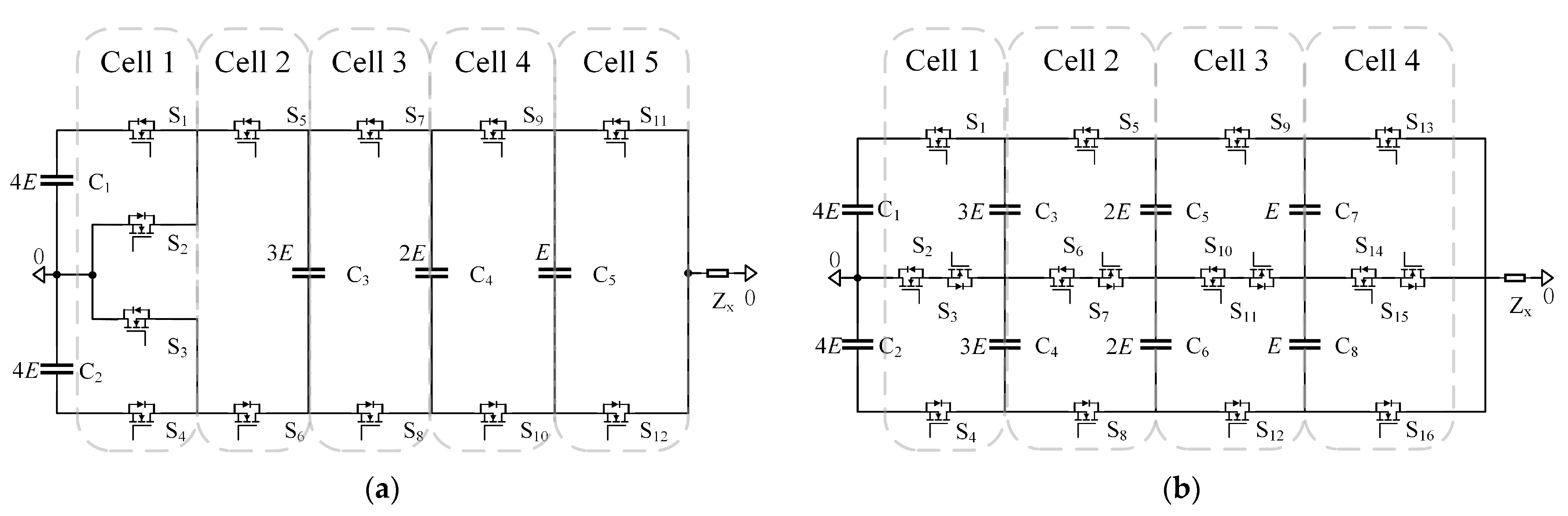
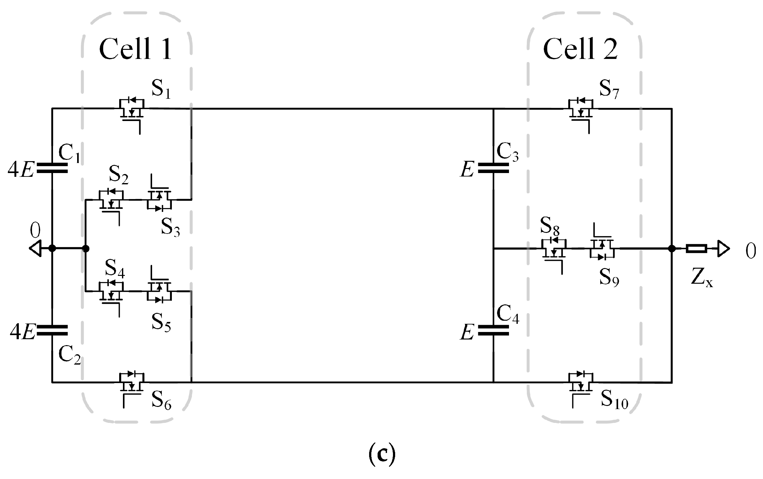
2.3. Comparison with Existing Nine-Level Inverter Topologies

In order to explain the advantages of the proposed topology more intuitively, this paper selects the traditional ANPC and SMC nine-level topology as the comparison objects. Figure 3 shows the above circuit topologies.
Table 2 presents the main circuit parameter comparison between the proposed topology and two typical nine-level topologies. In terms of the number of switching devices, the number of switching devices in the proposed topology is 5/8 than that of the SMC-9L topology and 5/6 than that of the ANPC-9L topology. The proposed topology can effectively reduce the difficulty of circuit design, reduce the system cost, and improve the reliability of the inverter. Compared with ANPC-9L, the number of floating capacitors in the proposed topology is reduced by 1, and 4 less than that of SMC-9L, and the withstand voltage is lower, which can reduce the volume of floating capacitors. In addition, the number of sensors of the proposed topology is also less than other topologies.
In order to compare the switching losses of the above three topologies, the ANPC-9L is divided into 5 units, the SMC-9L is divided into 4 units, and the proposed topology is divided into 2 units, as shown in Figure 3. It can be seen that the ANPC-9L unit 1 has the same structure as the unit 1 of the proposed topology, and the voltages of the devices are both 4E. Therefore, under the same switching frequency, the switching losses of the devices in the two topological units 1 are the same. The devices of ANPC-9L units 2, 3, 4, and 5 and the devices in the proposed topology unit 2 are both subjected to voltage E, but the proposed topology unit 2 has only 4 switching devices, while the ANPC-9L units 2, 2, There are a total of 8 switching devices in 3, 4 and 5. Obviously, at the same switching frequency, the proposed topology has smaller switching losses.
Compared with the SMC-9L, the proposed topology unit 2 and SMC-9L unit 4 have the same structure, and the voltages of the devices are both E. Under the same switching frequency, the switching loss of the proposed topology unit 2 and SMC-9L unit 4 is the same. There are 6 switching devices in the proposed topology unit 1, the withstand voltage is 4E, the number of switching devices in SMC-9L units 1, 2, and 3 is 12, and the device withstand voltage is E; thus, under the same switching frequency, the device switching loss of the unit 1 in proposed topology is slightly larger than that of the sum of the units 1, 2, 3 in SMC-9L.
Table 3 shows the comparison results of the total number of devices in the current path when the three nine-level topologies output different voltage levels. It can be seen that when the proposed topology outputs each level, the number of devices through which the current flows is the smallest, so the conduction loss is also the smallest. Generally, the switching frequency of a multilevel inverter is low, and the conduction loss accounts for the main part of the device loss. Therefore, the topology proposed in this paper has the lowest total device loss.

3. Control Strategy of Voltage Sensor without Floating Capacitance

The control objectives of the proposed nine-level inverter are: output voltage VO, dc-link capacitor voltages VC1, VC2, and flying capacitor voltages VC3, VC4. Since the one-dimensional space vector modulation algorithm has the advantages of high degree of freedom and can control multiple targets at the same time [26,27], the one-dimensional space vector modulation algorithm is adopted in this paper. On this basis, by analyzing the circuit state before the redundant switch state arrives, the estimation method of the floating capacitor voltage is given, and then the appropriate value is selected according to the difference between the estimated value of the floating capacitor voltage and the reference value and the positive and negative current of the current. Redundant switching state, a voltage sensor control algorithm without floating capacitance is proposed.

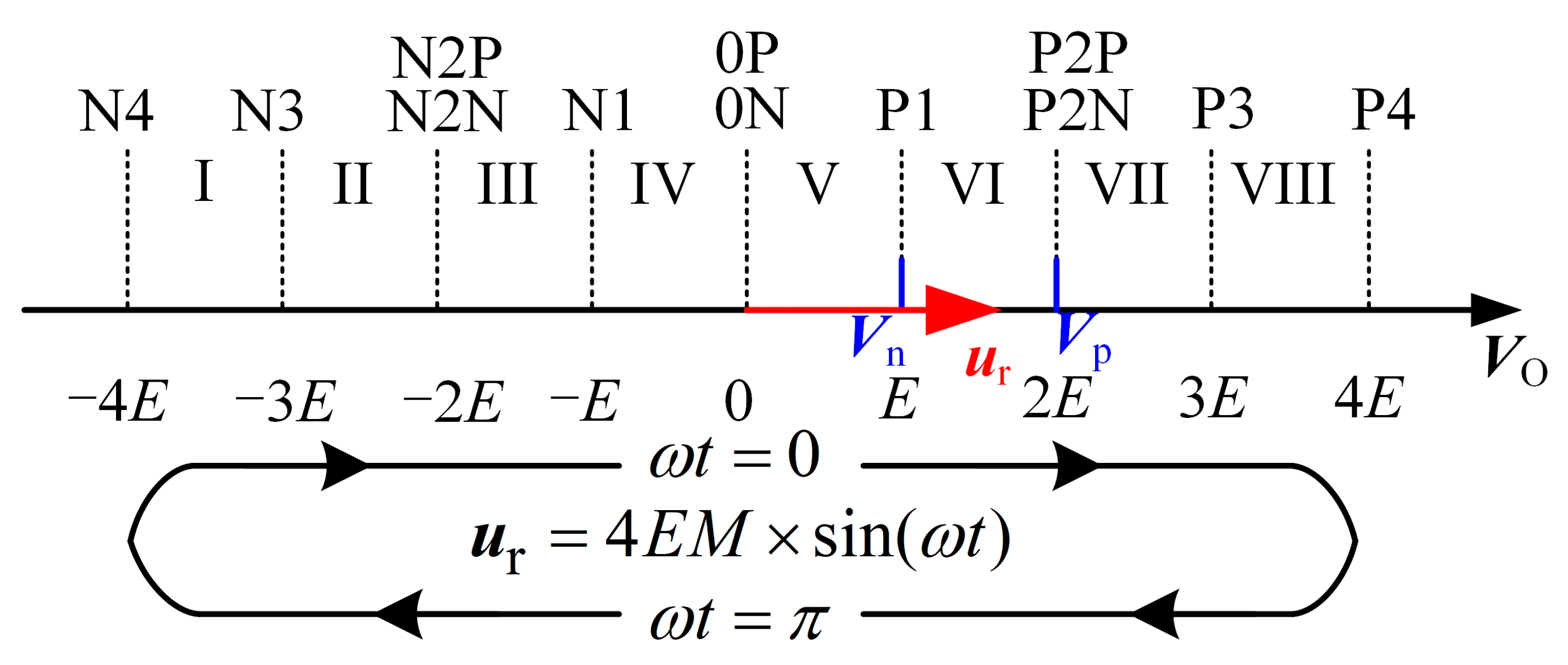
3.1. One-Dimensional Space Vector Modulation Algorithm

Let the output voltage vector of the single-phase nine-level inverter be VO, and the reference voltage vector be the modulating wave vector ur. Figure 4 shows the one-dimensional space vector diagram of the single-phase nine-level inverter.
The expression of the modulation signal ur is defined as
u r = 1 2 M V DC sin ( ω t ) ,
where M is the modulation degree, and 0 ≤ M ≤ 1. In the one-dimensional vector space, select the most recent two voltage vectors to synthesize the reference voltage ur. Let the vector with the larger modulus value be Vp, and the vector with the smaller modulus value be Vn. It can be noticed that the interval where ur is located can be determined according to the sign and modulus value of ur. If ur is in the interval VI, the vector 2E and E are used for synthesis.
According to volt-second balance principle, the dwell time of the vectors Vp and Vn satisfies Equation (2), where Ts is the switching period.
u r T s = V p T p + V n T n T s = T p + T n ,

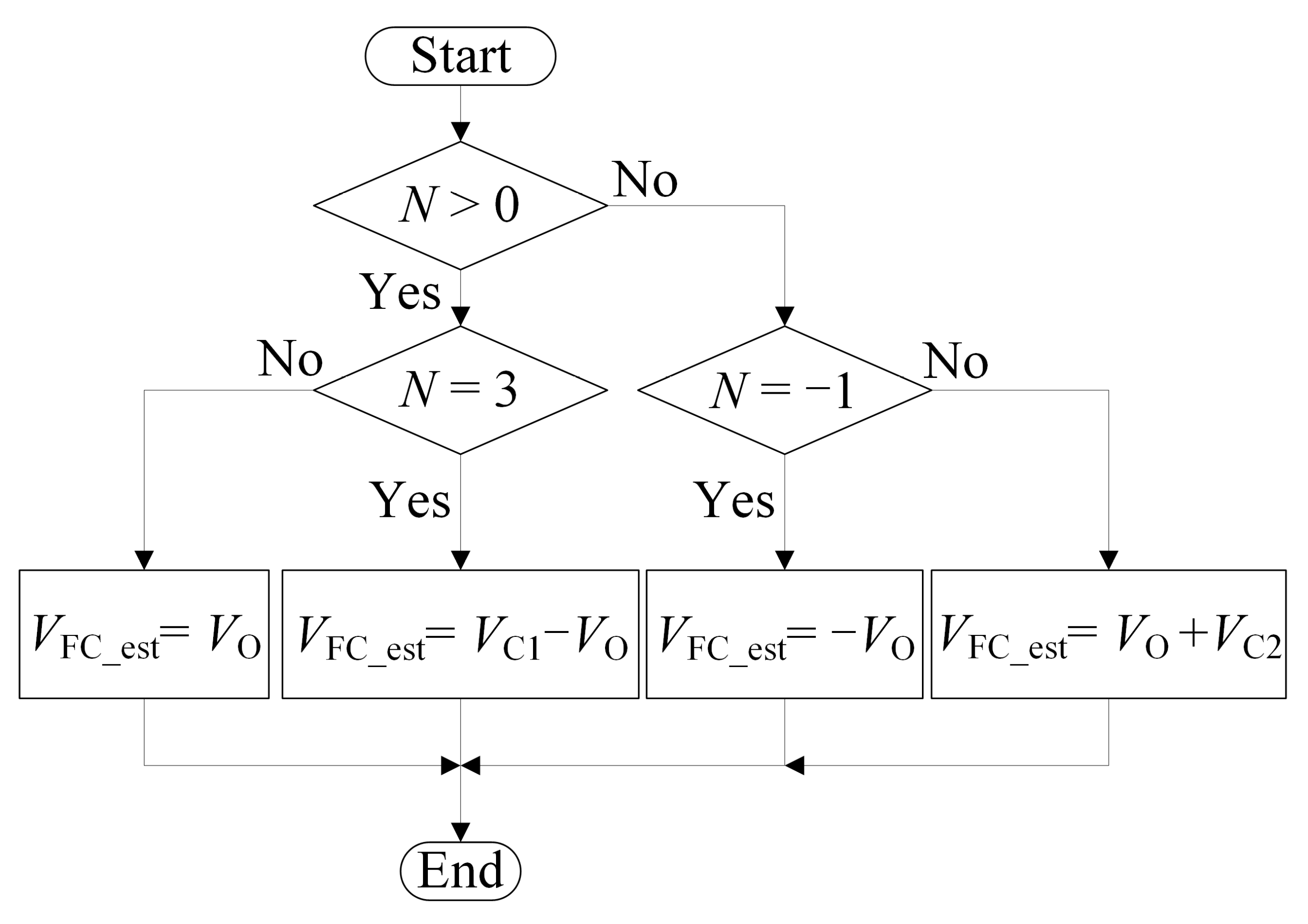
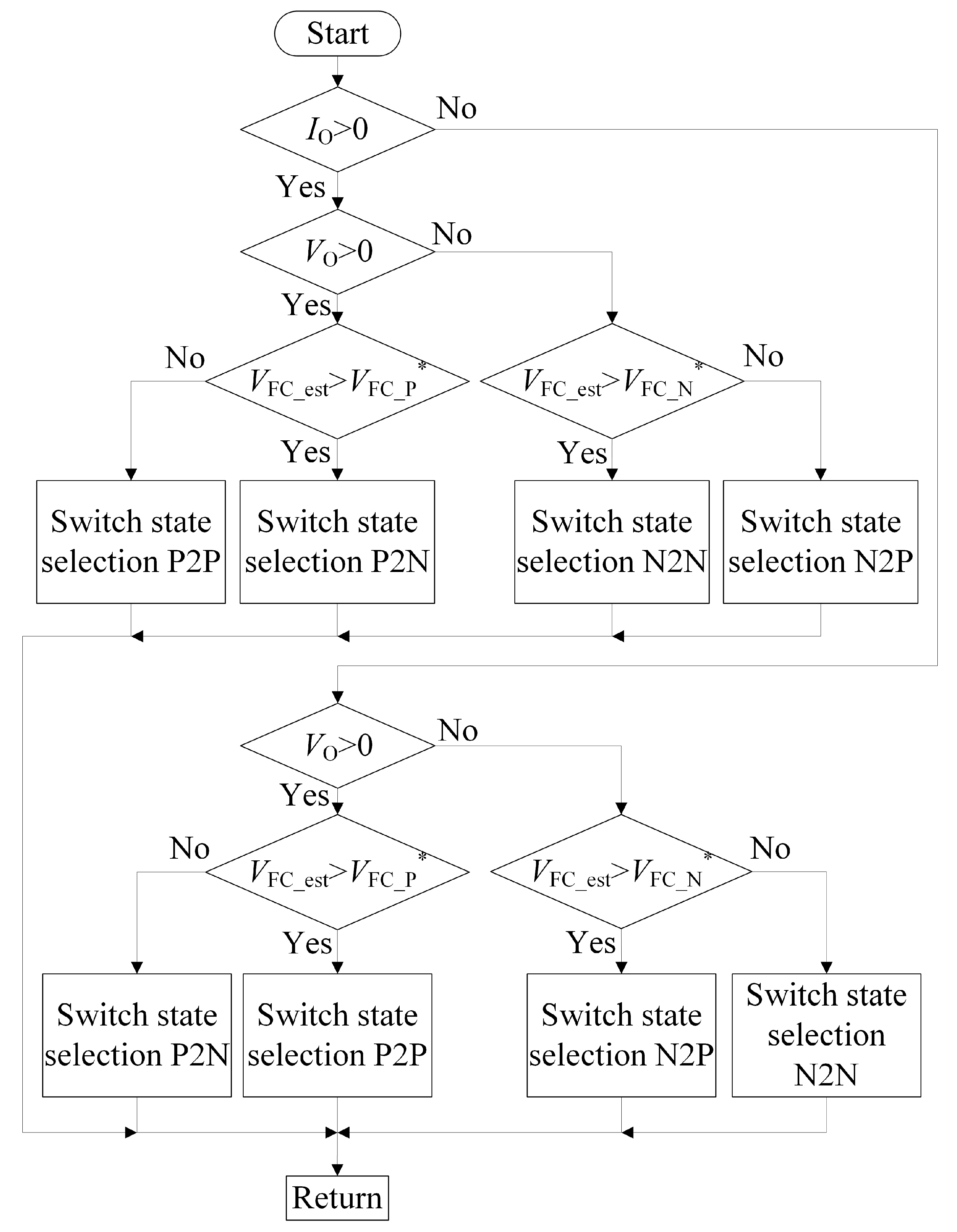
3.2. Control Strategy of Voltage Sensor without Floating Capacitance

From Table 1, the redundant switch states P2P, P2N, N2P and N2N can affect the floating capacitors C3 and C4 at the same time. Therefore, the floating capacitor voltage can be adjusted by reasonably selecting the redundant switch states corresponding to the ±2E level. In order to cancel the floating capacitor voltage sensor, it is necessary to accurately estimate the floating capacitor voltage before outputting the ±2E level.
Figure 5 shows the switch sequence diagram in which the output levels 2E and −2E participate. Before the output voltage reaches the 2E level, there are two level states, 3E and E. Therefore, it is necessary to perform voltage estimation in these two states. Taking Figure 5a as an example, the floating capacitor voltage value is estimated when the 3E level is output, and the redundant switch state selection is performed when the 2E level is output. Before the output voltage reaches the −2E level, there are two level states, −3E and −E, and the voltage needs to be estimated in these two states. In Figure 5c, when the output voltage is at the −E level, the floating capacitor voltage value is estimated, and the redundant switch state selection is performed when the output −2E level.
In order to distinguish the four level states of 3E, E, −E, and −3E, define the inverter output voltage to round up the level N:
N = ceil ( V O E ) ,
where ceil(x) is the round-up function.
As can be seen from Figure 5, there are 3 sampling data reading points in one switching sequence cycle, and the values of VC1, VC2, VO, and IO can be read at the sampling points. In Figure 2b, when the level state is 3E, the current flows through C1, C3 and the load and returns to the neutral point. According to Kirchhoff’s voltage law, the floating capacitor voltage VC3 can be expressed as VC1VO. In Figure 2h, when the level state is −E, the current flows through C3 and the load and returns to the neutral point, and the floating capacitor voltage VC3 can be expressed as −VO. Therefore, when the switch states are P3 and N1, the voltage of C3 can be estimated. In Figure 2e, when the level state is E, the current flows through C4 and the load and returns to the neutral point, and the floating capacitor voltage VC4 can be expressed as VO. When the flat state is −3E, the current flows through C2, C4 and the load and returns to the neutral point, and the floating capacitor voltage VC4 can be expressed as VO + VC2. Therefore, when the switching states are P1 and N3, the voltage of C4 can be estimated. Therefore, the voltage estimation formula of capacitors C3 and C4 can be expressed as:
V FC _ est = V C 1 V O , V O = 3 E V O , V O = E V O , V O = E V O + V C 2 , V O = 3 E ,
However, when voltage estimation is performed, there will be cases where the estimated value changes abruptly as the switch state changes. Therefore, it is necessary to deal with this sudden change in the control algorithm: use the estimated value at the previous moment to select the redundant switch state, so as to avoid the sudden change in the estimated value causing the estimated voltages of C3 and C4 to be unbalanced.
Since the proposed topology and modulation signal ur are both symmetrical, in theory, the charge and discharge capacities of capacitors C3 and C4 are not much different, and the redundant switch states at 2E and −2E levels have the same effect on the charge and discharge of C3 and C4. Therefore, it is not necessary to set the priority of voltage regulation of C3 and C4 in the proposed control algorithm, and unified tracking regulation can be performed according to the estimated floating capacitor voltage value corresponding to the moment before the arrival of the output level ±2E. Let ΔVCF be the voltage offset state between the estimated value of C3 or C4 and the reference value, the polarity of the voltage offset of C3 and C4 can be expressed as:
D C = 1 ,   Δ V CF > 0 0 ,   Δ V CF 0 ,
Let the direction of the current flowing out of the inverter be the positive direction, and the current direction is represented by DI:
D I = 1 ,   i O > 0 0 ,   i O 0 ,
It can be seen from the literature [28] that the selection of the reference value of the floating capacitor voltage determines the storage and transmission of capacitive energy in the topology, and the transfer relationship of the capacitive energy is:
Δ Q C 1 + Δ Q FC _ P = Δ Q C 2 + Δ Q FC _ N ,
In the formula, ΔQC1 and ΔQC2 are the energy transferred from C1 and C2 to the load in one modulating wave cycle, respectively; ΔQFC_P and ΔQFC_N are the energy transferred from C3 and C4 to the load in the positive and negative half cycles. Therefore, the voltage reference value of the positive and negative half-cycle floating capacitors can be set as:
V FC _ P * = E + K ( 2 E V C 2 2 ) ,
V FC _ N * = E + K ( 2 E V C 1 2 ) ,
In the formula, K is the voltage correction coefficient, and the value of K affects the balance degree of VC1 and VC2.
When the estimated voltage of the floating capacitor C3 or C4 is greater than or less than the reference voltages VFC_P* and VFC_N*, it needs to be discharged or charged, and then the switch state at the next moment is selected according to the direction of the output current IO at this time. When the inverter outputs 2E and −2E levels, the switching state selection principle for balancing the voltage of the floating capacitor is as follows:
S P 2 = D C D I * P 2 P + D C D I * P 2 N ,
S N 2 = D C D I * N 2 P + D C D I * N 2 N .

3.3. Implementation of the Proposed Algorithm

The implementation process of the floating capacitor voltage estimation is shown in Figure 6. By judging the size of the output voltage rounding up the level N, the estimation formula of the floating capacitor voltage is selected.
The flowchart of redundant switch state selection is shown in Figure 7. Combined with Table 1, if the sampled output current IO > 0 and the output voltage VO is positive, when the estimated value of the floating capacitor voltage is greater than the reference value, select the P2N switch state to discharge; when the estimated value of the floating capacitor voltage is less than the reference value, select the P2P switching state for charging, so that the voltage of the floating capacitor returns to a balanced state. Similarly, other redundant switch states can be selected according to Figure 7.
The block diagram of the proposed control strategy is shown in Figure 8. The nine-level inverter adopts one-dimensional space vector modulation, obtains the real-time operating parameters VC1, VC2, VO, IO of the inverter through sampling, selects the calculation formula of the floating capacitor voltages according to the redundant switch state, judges the positive and negative output current. Then, calculate the difference between the estimated value of the floating capacitor voltage and the reference value, and select the redundant switch state according to the charging and discharging requirements of the floating capacitor, and finally output the driving pulse of the switch tube Sk (k = 1, 2, … 7).

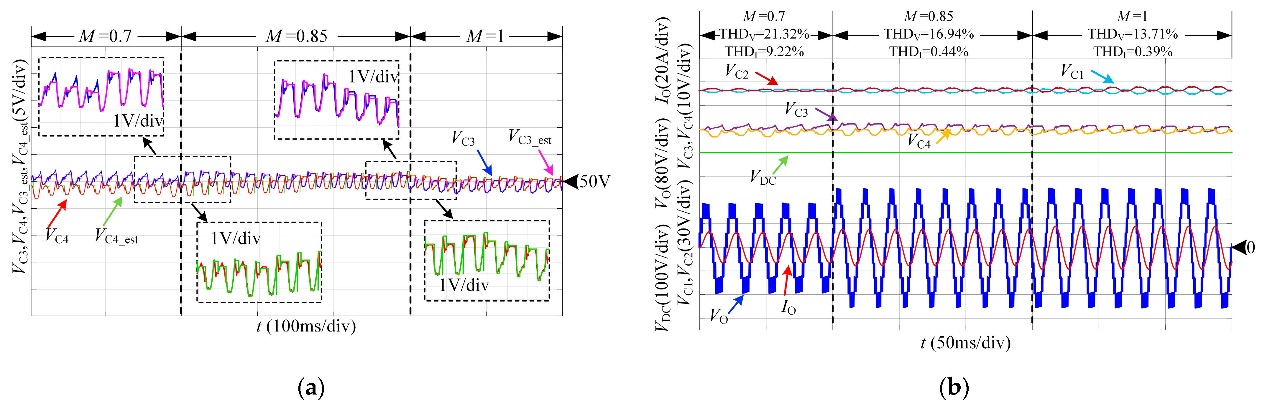
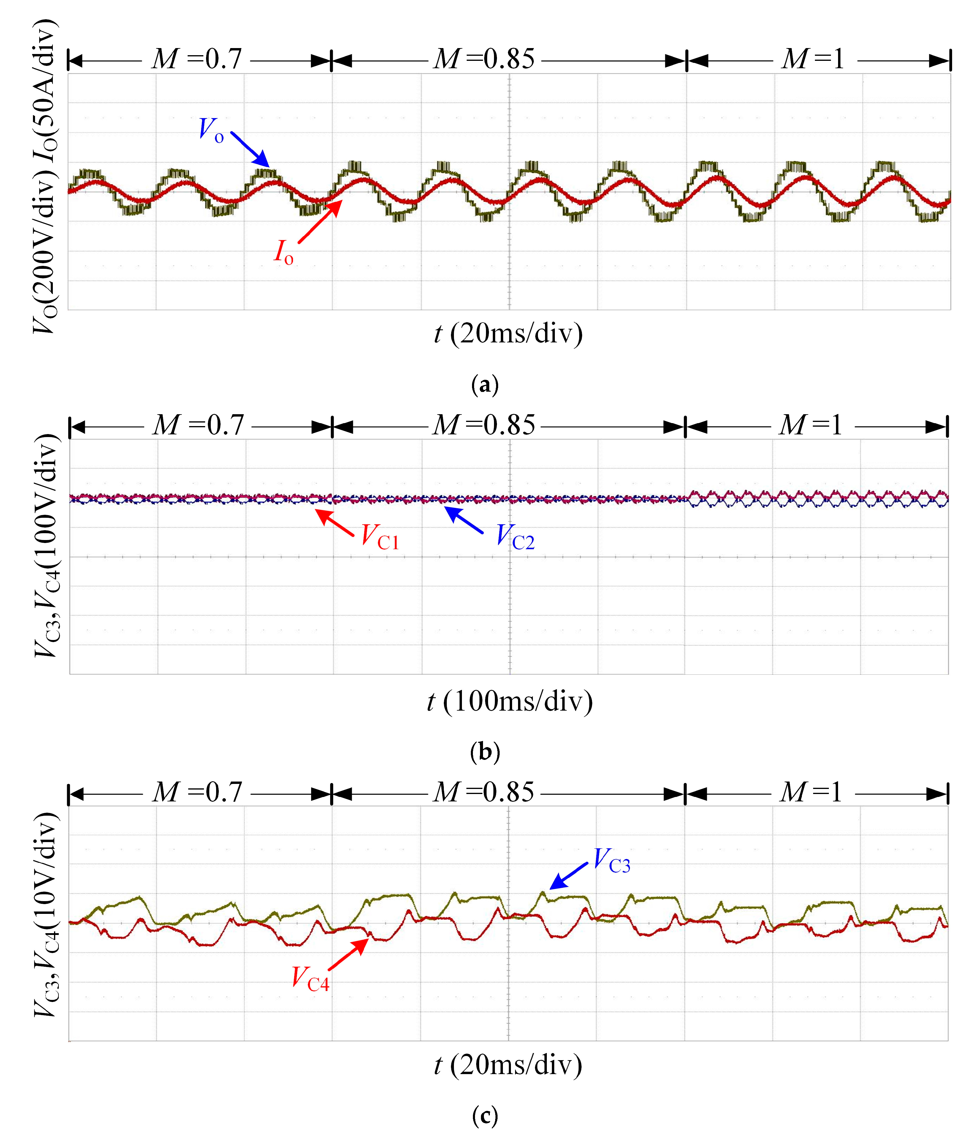
4. Simulation and Experimental Analysis

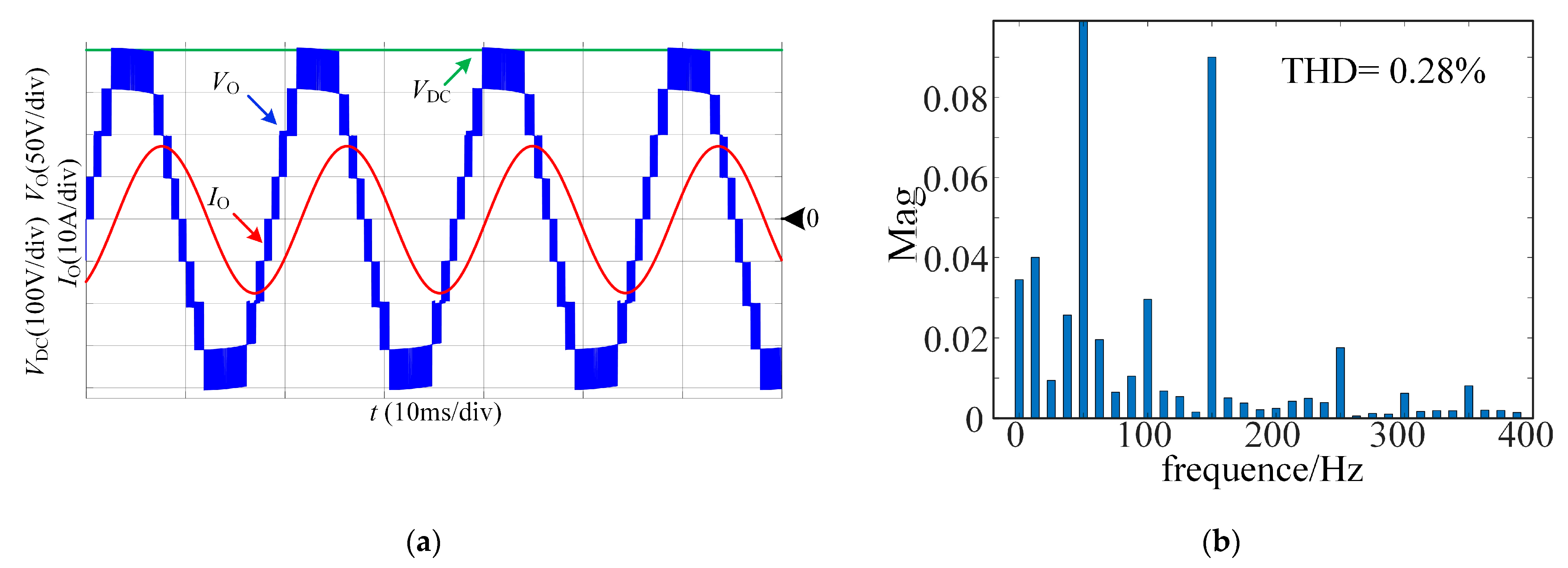
4.1. Simulation Analysis

In order to verify the validity of the proposed topology and the feasibility of the control strategy, a single-phase nine-level inverter simulation model was built in Matlab/Simulink. The simulation parameters are listed as follows: dc-link voltage reference value is 400 V, bus capacitor C1 = C2 = 6720 uF, flying capacitor C3 = C4 = 6 mF, output voltage fundamental frequency is 50 Hz, load Lf = 30 mH, Rf = 10 Ω. The voltage correction coefficient K in Equations (8) and (9) is tuned as 0.1.
Figure 9 shows the steady-state simulation waveforms of the proposed topology. It can be seen from Figure 9a,b that the output voltage of the proposed topology is a nine-level staircase wave, the output current has a high sine degree, and the current THD is 0.28%. In Figure 9c, the bus capacitor voltage is stable around 200 V, with a fluctuation range of ±3.8 V, and the floating capacitor voltage is stable around 50 V, with an up and down fluctuation range of ±2.2 V.
Figure 10 shows the simulation waveforms of the dc-link voltage, bus capacitor voltage, floating capacitor voltage, output voltage and output current when the modulation factor M = 0.7, M = 0.85 and M = 1. THDV and THDI are the THD values of the output voltage and output current, respectively. It can be seen from Figure 10 that when the modulation degree is small, the output voltage presents a seven-level staircase wave. When the modulation degree changes, the output voltage can achieve a smooth transition. Under different modulations, both the bus capacitor voltage and the floating capacitor voltage are stable near their reference values, where the bus capacitor voltage ripple is 7 V, and the floating capacitor voltage ripple is 5 V.
Figure 11 shows the simulation waveforms of the proposed voltage sensorless control strategy. It can be seen from Figure 11a that the proposed control method can track the voltage of the floating capacitor quickly and accurately under different modulation degrees, and the error rate is less than 2%. Comparing Figure 10 and Figure 11b, the proposed method has the same output performance as the traditional sensor measurement method, but its capacitor voltage ripple is larger than that of the sensor measurement, the bus capacitor voltage ripple is 13 V, and the floating capacitor voltage ripple is 7 V. Because the floating capacitor voltage estimation method is affected by the sampling time and the system calculation time, a slight delay leads to a larger estimation error.

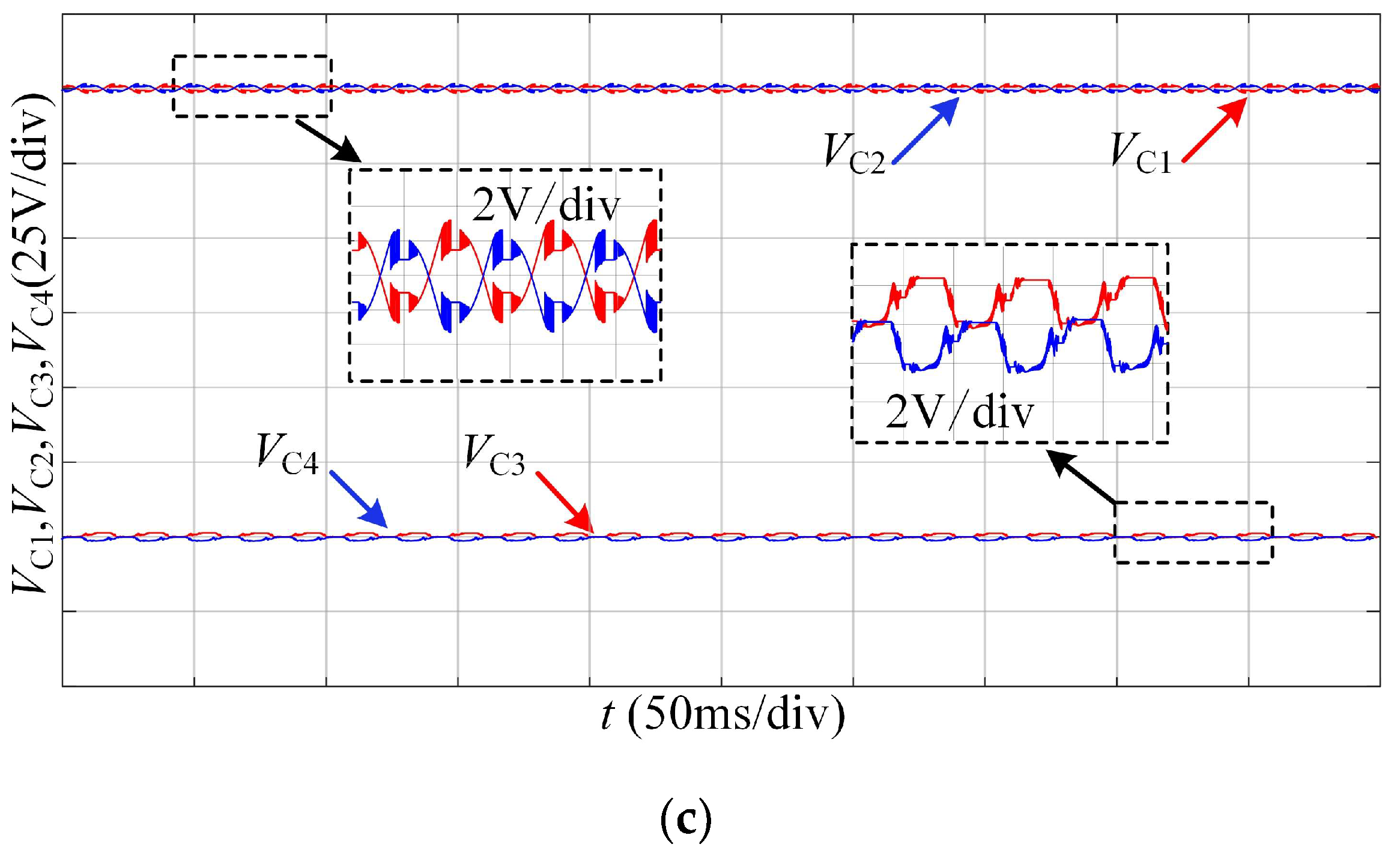
4.2. Experimental Analysis

To further verify the effect of the circuit topology and control method proposed in this paper, an experimental platform is built, as shown in Figure 12. The experimental parameters are as follows: dc-link voltage reference value is 400 V, dc-link capacitor C1 = C2 = 6720 uF, floating capacitor C3 = C4 = 6 mF, output voltage fundamental frequency fg = 50 Hz, load Lf = 30 mH, Rf = 6 Ω, and system switch Frequency fs = 2 kHz. The switch device model used in this platform is IPW60R070C6, and its driver is QC962-8A.
Figure 13 shows the experimental waveforms of the proposed topology at different modulation degrees. In Figure 13a, the experimental waveform is basically consistent with the simulation result, the output voltage is a nine-level staircase wave, and the output current has a high sine degree. Due to the influence of the load inductance Lf, the current lags the voltage. It can be seen that the nine-level topology has good output performance. It can be seen from Figure 13b that VC1 and VC2 are both stable at about 200 V, and the voltage fluctuation range is ±12 V. It can be seen from Figure 13c that VC3 and VC4 are both stable at about 50 V, and the voltage fluctuation range is ±4 V.
Figure 14 shows the experimental waveforms of the proposed voltage sensorless control strategy. It can be seen from Figure 14a that under different modulation degrees, the proposed method has the same effect as using the floating capacitor voltage sensor, and both can achieve stable output of the inverter. In Figure 14b, VC1 and VC2 have the smallest ripple when M = 0.85, and the voltage ripple range is ±14 V. From Figure 14c, it can be noticed that the voltage fluctuation range of VC3 and VC4 is ±8 V, which is slightly larger than that of the method with floating capacitor voltage sensor. It is because the voltage ripple is affected by factors such as the control frequency of the system, the correction coefficient K, and the number of estimated sampling points. Although the voltage ripple is large, the proposed sensorless control strategy can reduce the hardware cost of the system, since there is no need to design the sampling circuit of the floating capacitor voltages.

5. Conclusions

This paper proposes a single-phase non-isolated nine-level inverter topology. Compared with the traditional topology, this topology has the advantages of fewer switching devices and fewer floating capacitors. Additionally, a floating capacitor voltage sensorless control algorithm is presented. The algorithm realizes the estimation of the floating capacitor voltages by sampling the output voltage and the bus capacitor voltage, and it achieves the balance of the floating capacitor voltages combined with the one-dimensional space vector modulation method. Finally, the proposed algorithm is verified by computer simulation and experiments. Theoretical analysis and simulation experimental results show that the proposed topology and control method have the following advantages:
(1)
Compared with the traditional nine level inverter topology, the proposed nine level inverter has obvious advantages in the number of switching devices and the number of flying capacitors. The most prominent is that the number of switching devices through which the current flows is the least, which reduces the device switching loss in the inverter.
(2)
The proposed method reduces 50% capacitor voltage sampling circuit, which can greatly reduce the cost of the system, and it can realize the accurate estimation of the floating capacitor voltage and its balance control at a specific moment.

Author Contributions

Conceptualization, Y.L. and Y.S.; methodology, Y.L., W.H., B.L. and Y.S.; software, W.H. and B.L.; validation, Y.L., Z.L. and W.H.; formal analysis, W.H. and B.L.; writing—original draft preparation, Y.L. and Y.S.; writing—review and editing, W.H. and B.L. All authors have read and agreed to the published version of the manuscript.

Funding

This research was funded by the National Science Foundation of China (No.61273251) and open Project of National and Local Joint Engineering Laboratory of High Energy-saving Motor and Control Technology of Anhui University (KFKT202104).

Institutional Review Board Statement

Not applicable.

Informed Consent Statement

Not applicable.

Data Availability Statement

Not applicable.

Acknowledgments

The authors gratefully appreciate the reviewers for their constructive comments and suggestions.

Conflicts of Interest

The authors declare no conflict of interest.

References

  1. Wang, Y.Q.; Ku, R.H.; Zhou, C.L.; Wang, Z.; Wang, M.D. Hybrid T-type multilevel inverter and its modulation strategy. High Volt. Eng. 2020, 46, 3220–3228. [Google Scholar]
  2. Yu, H.Y.; Chen, B.; Yao, W.X.; Liu, Z.Y. Hybrid seven-level converter based on t-type converter and h-bridge cascaded under SPWM and SVM. IEEE Trans. Power Electron. 2018, 33, 689–702. [Google Scholar] [CrossRef]
  3. Zhang, Y.L.; Wang, Q.J.; Hu, C.G.; Zhou, Y.F. A novel low voltage seventeen-level converter and control strategy. Proc. CSEE 2020, 40, 1095–1105. [Google Scholar]
  4. Yousofi-Darmian, S.; Barakati, S.M. A new asymmetric multilevel inverter with reduced number of co-mponents. IEEE J. Emerg. Sel. Top. Power Electron. 2020, 8, 4333–4342. [Google Scholar] [CrossRef]
  5. Hu, C.G.; Rui, T.; Ma, D.J.; Wang, Q.J.; Luo, F.L. SVM control strategy for neutral point voltage balance and switching loss reduction of three-level ANPC inverter. Proc. CSEE 2016, 36, 3598–3608. [Google Scholar]
  6. Cao, Y.; Yang, J.T.; Li, R.; Cai, X.; Yu, W.; Xu, J.; Du, C.R.; Huang, L.; Zhang, T.; Ma, Z.Y.; et al. Circulating current suppression strategy of ANPC nine-level inverter. Proc. CSEE 2020, 40, 232–242. [Google Scholar]
  7. Viju, N.R.; Arun, R.S.; Kaarthik, R.S. Generation of higher number of voltage levels by stacking inverters of lower multilevel structures with low voltage devices for drives. IEEE Trans. Power Electron. 2017, 32, 52–59. [Google Scholar]
  8. Liu, J.F.; Wu, J.L.; Zeng, J.; Guo, H.F. A novel nine-level inverter employing one voltage source and reduced components as high-frequency AC power source. IEEE Trans. Power Electron. 2017, 32, 2939–2947. [Google Scholar] [CrossRef]
  9. Ghias, A.M.Y.M.; Pou, J.; Agelidis, V.G. An active voltage-balancing method based on phase-shifted PWM for stacked multicell converters. IEEE Trans. Power Electron. 2016, 31, 1921–1929. [Google Scholar] [CrossRef]
  10. Ghias, A.M.Y.M.; Pou, J.; Acuna, P.; Ceballos, S.; Heidari, A.; Agelidis, V.G.; Merabet, A. Elimination of low-frequency ripples and regulation of neutral-point voltage in stacked multicell converters. IEEE Trans. Power Electron. 2017, 32, 164–175. [Google Scholar] [CrossRef]
  11. Lee, S.S.; Sidorov, M.; Lim, C.S. Hybrid cascaded multilevel inverter (HCMLI) with improved symmetrical 4-Level submodule. IEEE Trans. Power Electron. 2018, 33, 932–935. [Google Scholar] [CrossRef]
  12. Sandeep, N.; Yaragatti, U.R. Design and implementation of a sensorless multilevel inverter with reduced part count. IEEE Trans. Power Electron. 2017, 33, 6677–6683. [Google Scholar] [CrossRef]
  13. Sandeep, N.; Yaragatti, U.R. Operation and control of a nine-level modified ANPC inverter topology with reduced part count for grid-connected applications. IEEE Trans. Ind. Electron. 2018, 65, 4810–4818. [Google Scholar] [CrossRef]
  14. Liu, C.K.; Deng, F.J.; Wang, Q.J.; Wang, Y.B.; Blaabjerg, F.; Wang, Z. Double half-bridge submodule-based modular multilevel converters with reduced voltage sensors. IEEE Trans. Power Electron. 2021, 36, 3643–3648. [Google Scholar] [CrossRef]
  15. Li, J.J.; Jiang, J.G. A novel space vector pulse width modulation for five-level nested neutral point piloted converter. Proc. CSEE 2018, 38, 3306–3315. [Google Scholar]
  16. Hu, C.G.; Dong, H.; Zhang, Y.L.; Li, J. Hybrid active neutral clamped seven level inverter and its control strategy. Electr. Mach. Control 2020, 24, 40–49. [Google Scholar]
  17. Sandeep, N.; Yaragatti, U.R. A switched-capacitor-based multilevel inverter topology with reduced components. IEEE Trans. Power Electron. 2018, 33, 5538–5542. [Google Scholar] [CrossRef]
  18. Cheng, Q.; Wang, C.; Chen, Z.; Li, Z. A capacitor-voltage-balancing method based on optimal zero-sequence voltage injection in stacked multicell converter. IEEE J. Emerg. Sel. Top. Power Electron. 2021, 9, 4700–4714. [Google Scholar] [CrossRef]
  19. Davis, T.T.; Joseph, T.; Dey, A. A capacitor voltage balancing scheme for single-source fed switch optimized three-phase nine-level inverter. IEEE Trans. Ind. Electron. 2021, 68, 3652–3661. [Google Scholar] [CrossRef]
  20. Tian, K.; Wu, B.; Narimani, M.; Xu, D.; Cheng, Z.Y.; Zargari, N.R. A capacitor voltage-balancing method for nested neutral point clamped (NNPC) inverter. IEEE Trans. Power Electron. 2016, 31, 2575–2583. [Google Scholar] [CrossRef]
  21. Wang, K.; Xu, L.; Zheng, Z.D.; Li, Y.D. Voltage balancing control of a four-level hybrid-clamped converter based on zero-sequence voltage injection using phase-shifted PWM. IEEE Trans. Power Electron. 2016, 31, 5389–5399. [Google Scholar] [CrossRef]
  22. Li, W.C.; Ma, W.M.; Wang, G.G.; Lin, C.M.; Lie, S.X.; Guo, D.H. Novel space vector pulse width modulation method for neutral point clamped H-bridge cascaded single-phase inverter. Proc. CSEE 2014, 34, 5313–5319. [Google Scholar]
  23. Liu, B.; Feng, X.Y.; Deng, R.; Xia, W.J.; Song, W.S. Grid voltage sensorless control strategy of single-phase PWM rectifiers with model reference adaptive system. Proc. CSEE 2019, 39, 6065–6074. [Google Scholar]
  24. Zhang, L.H.; Born, R.; Gu, B.; Chen, B.F.; Zheng, C.; Zhao, X.N.; Lai, J.S. A sensorless implementation of the parabolic current control for single-phase stand-alone inverters. IEEE Trans. Power Electron. 2016, 31, 3913–3921. [Google Scholar] [CrossRef]
  25. Viswadev, R.; Mudlapur, A.; Ramana, V.V.; Venkatesaperumal, B.; Mishra, S. A novel AC current sensorless hysteresis control for grid tie inverters. IEEE Trans. Circuits Syst. II 2020, 67, 2577–2581. [Google Scholar] [CrossRef]
  26. Leon, J.I.; Portillo, R.; Vazquez, S.; Padilla, J.J.; Franquelo, L.G.; Carrasco, J.M. Simple unified approach to develop a time-domain modulation strategy for single-phase multilevel converters. IEEE Trans. Ind. Electron. 2008, 55, 3239–3248. [Google Scholar] [CrossRef]
  27. Liu, F.; Wu, X.Z.; Zhao, Y.M.; Liu, J.D.; Zhang, P.; Zhao, Y.X.; Wang, J. Research on common mode voltage suppression technology of multilevel inverter based on one-dimensional space vector modulation. Power Syst. Technol. 2020, 44, 3972–3982. [Google Scholar]
  28. Teymour, H.R.; Sutanto, D.; Muttaqi, K.M.; Cinfo, P. A novel modulation technique and a new balancing control strategy for a single-phase five-level ANPC converter. IEEE Trans. Ind. Appl. 2015, 51, 1215–1227. [Google Scholar] [CrossRef]
Figure 1. The topology of the proposed 9-level converter.
Energies 15 03418 g001
Figure 2. Operating states of the proposed 9-level topology. (a) VO = 4E; (b) VO = 3E; (c) VO = 2E; (d) VO = 2E; (e) VO = E; (f) VO = 0; (g) VO = 0; (h) VO = −E; (i) VO = −2E; (j) VO = −2E; (k) VO = −3E; (l) VO = −4E.
Energies 15 03418 g002aEnergies 15 03418 g002b
Figure 3. The topology of the three nine-level converters. (a) ANPC-9L; (b) SMC-9L; (c) The proposed topology.
Energies 15 03418 g003aEnergies 15 03418 g003b
Figure 4. One-dimensional SVM of the proposed 9-level converter.
Energies 15 03418 g004
Figure 5. The switching sequences that contain the 2E, −2E voltage vector. (a) N = 3; (b) N = 1; (c) N = −1; (d) N = −3.
Energies 15 03418 g005
Figure 6. The flow chart of floating capacitor voltage estimation.
Energies 15 03418 g006
Figure 7. The flow chart of redundant switching states selection.
Energies 15 03418 g007
Figure 8. The block diagram of the proposed floating capacitor voltage sensorless control scheme.
Energies 15 03418 g008
Figure 9. Simulation waveforms of the proposed topology in the steady-state. (a) Bus voltage output voltage and output current simulation waveform; (b) Output current FFT analysis results; (c) Simulation Waveforms of dc-link Capacitor Voltage and Suspended Capacitor Voltage.
Energies 15 03418 g009aEnergies 15 03418 g009b
Figure 10. Simulation results under different modulation degree M.
Energies 15 03418 g010
Figure 11. Simulation waveforms of the proposed floating capacitor voltage sensorless control scheme. (a) Simulation waveform of actual and estimated value of floating capacitor voltage; (b) Capacitor voltage, output voltage and output current simulation waveforms.
Energies 15 03418 g011
Figure 12. Scaled-down experimental platform of the proposed single-phase nine-level inverter.
Energies 15 03418 g012
Figure 13. Experimental results of the proposed inverter with different M. (a) Output voltage VO and output current IO waveform; (b) dc-link capacitor voltage VC1, VC2 waveform; (c) Suspension capacitor voltage VC3, VC4 waveform.
Energies 15 03418 g013
Figure 14. Experimental results of the floating capacitor voltage sensorless control scheme. (a) Waveforms of the output voltage VO and output current IO; (b) Waveforms of the dc-link capacitor voltages VC1, VC2; (c) Waveforms of the capacitor voltage VC3, VC4.
Energies 15 03418 g014
Table 1. Switching states of the proposed 9-level converter.
S1–S7StatesVC3VC4VO
IO > 0IO < 0IO > 0IO < 0
1000100P4----4E
1000001P3--3E
1000010P2P2E
0010100P2N2E
0010001P1--E
0100100OP----0
0010010ON----0
0100001N1--E
0100010N2P−2E
0001100N2N−2E
0001001N3-- −3E
0001010N4----−4E
Note: ‘↑’ means capacitor charging; ‘↓’ means capacitor discharge.
Table 2. Parameters comparison of the main circuit.
ParametersANPC-9LSMC-9LProposed Topology
number of switching devices121610
switching devices withstand voltage4E × 4 + E × 8E × 164E × 6 + E × 4
capacitive voltage sensing number of devices584
number of floating capacitors362
suspension capacitance withstand voltage3E × 1 + 2E × 1 + E × 13E × 2 + 2E × 2 + E × 2E × 2
Table 3. Comparison of the total number of devices in the current path.
VOTotal Number of Devices in the Current Path
ANPC-9LSMC-9LProposed Topology
4E542
3E553
2E562
E574
0583
−E574
−2E562
−3E553
−4E542
Publisher’s Note: MDPI stays neutral with regard to jurisdictional claims in published maps and institutional affiliations.

