
A Comprehensive Review on Common-Mode Voltage of Three-Phase Quasi-Z Source Inverters for Photovoltaic Applications

 , ,
, ,  and
and
Abstract
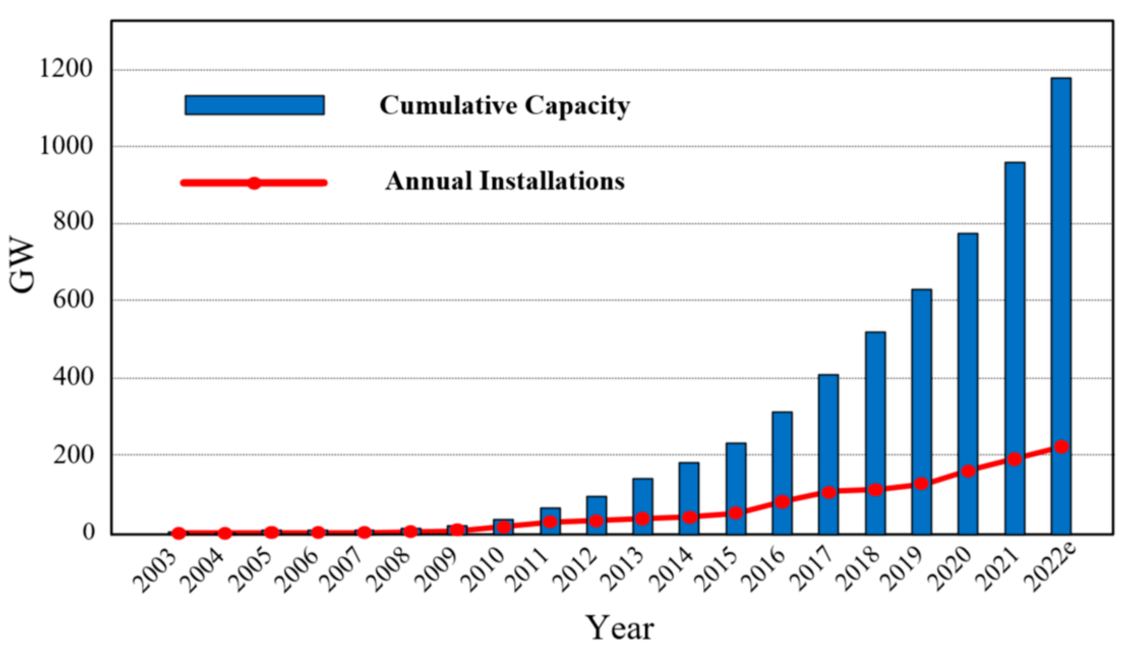
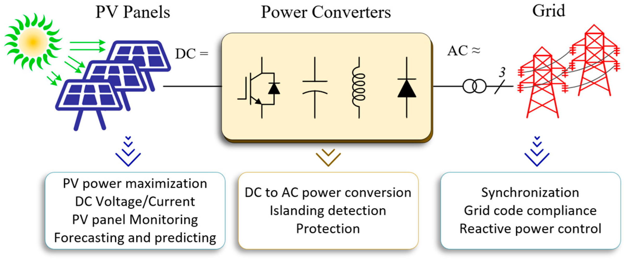
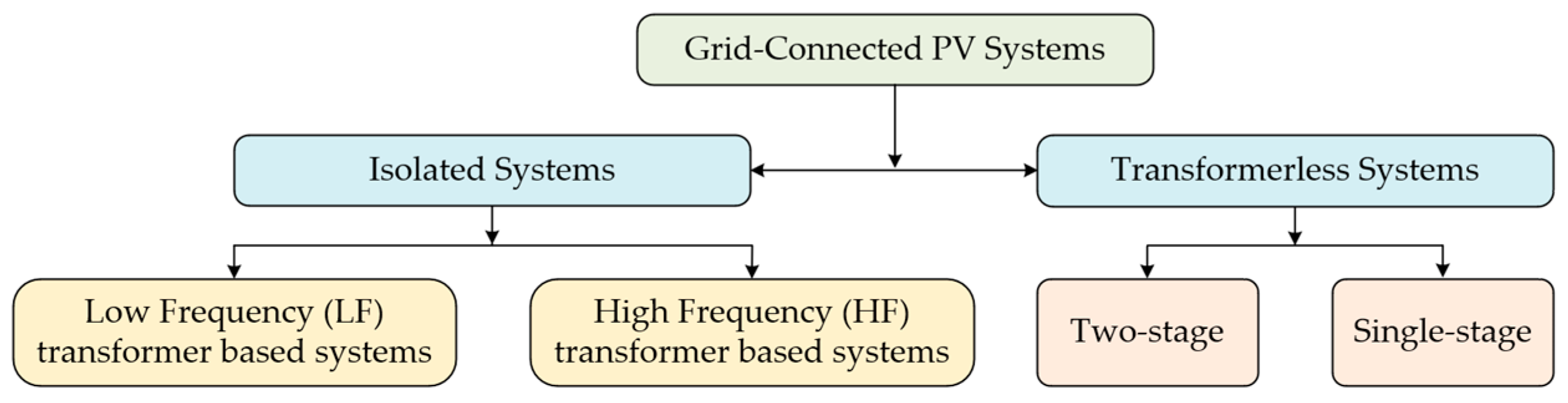
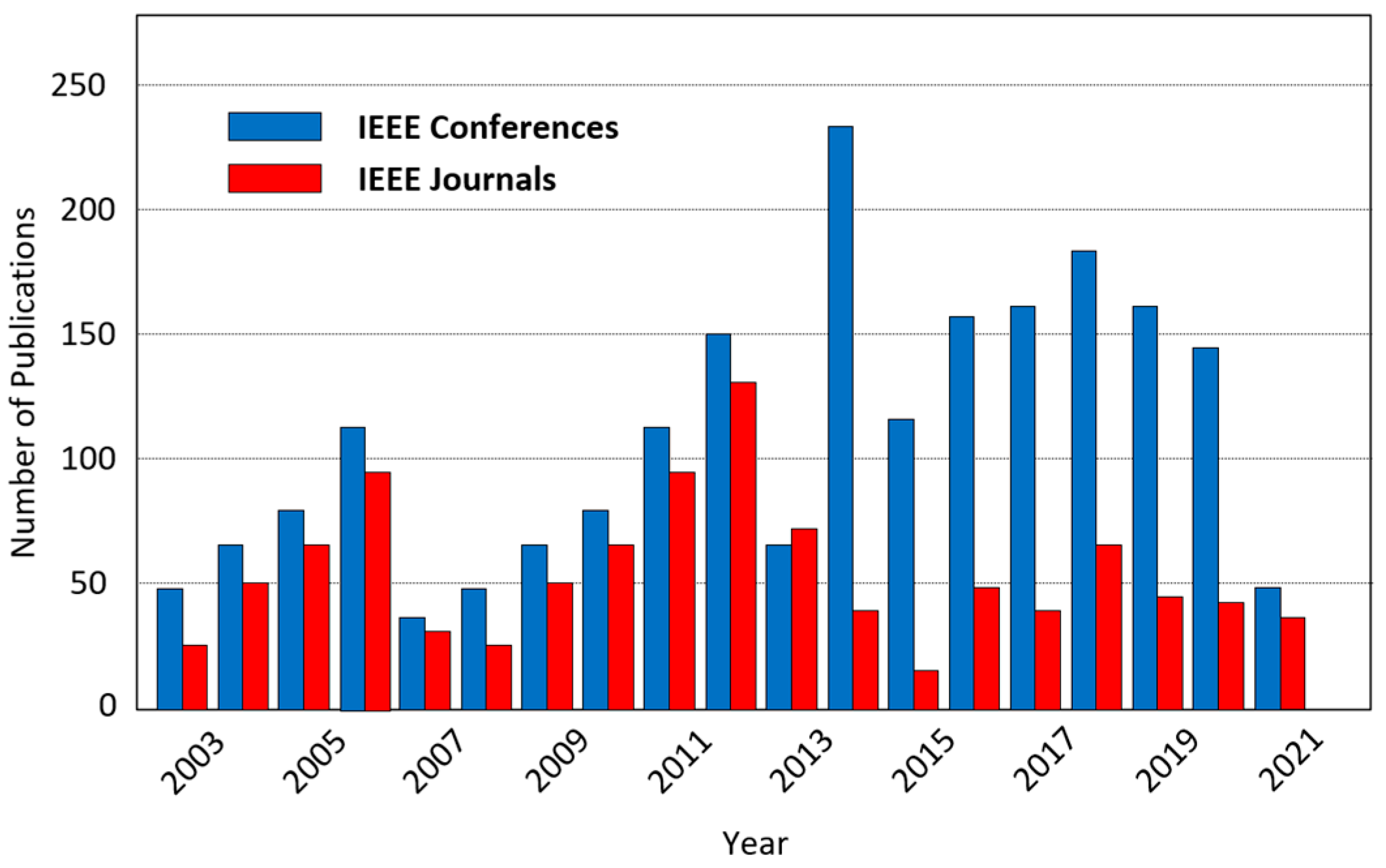
:1. Introduction
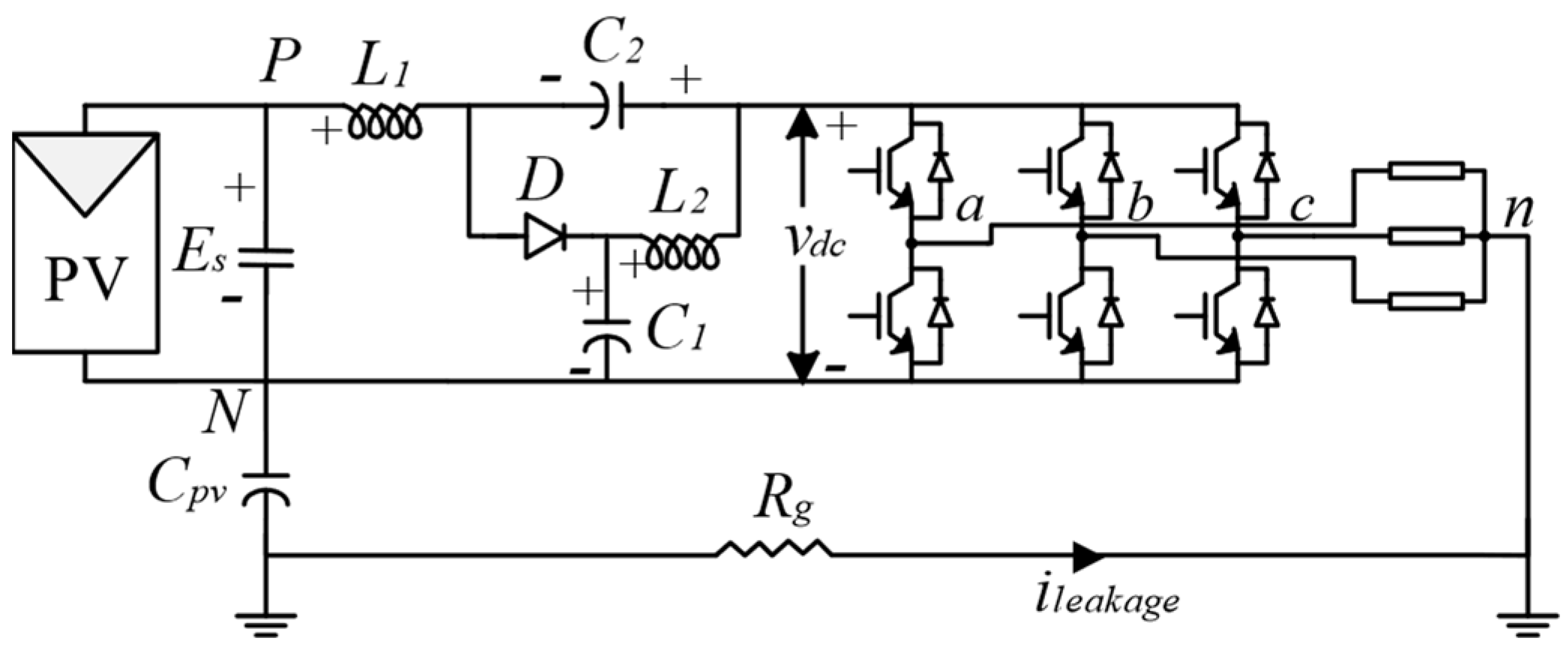
2. Operating Principles of QZSI
2.1. Non-ST Mode
2.2. ST Mode
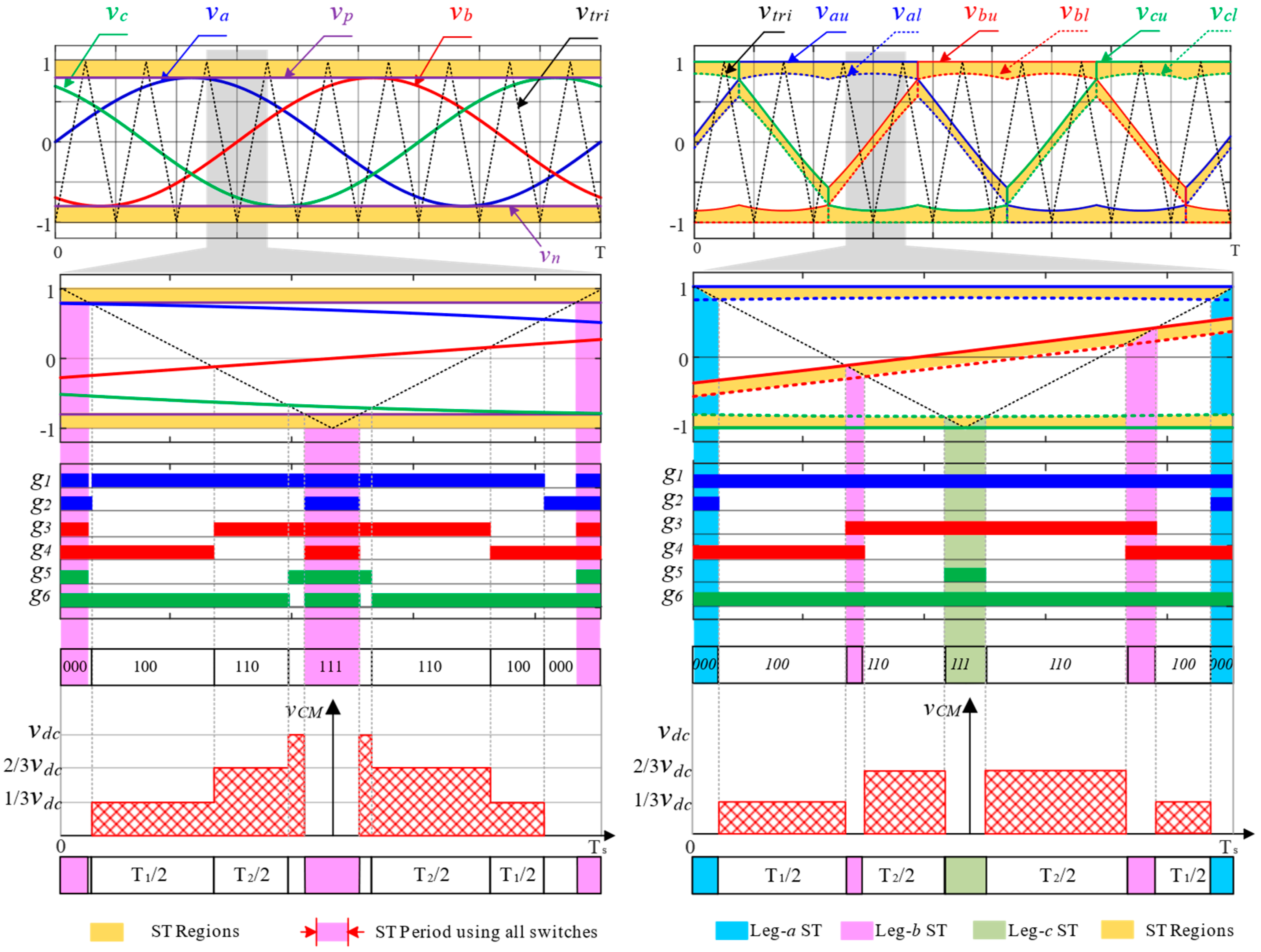
3. Review of PWM Techniques for QZSI
4. CMV in QZSI
4.1. CMV—Root Mean Square
4.2. Maximum Value of CMV and Its
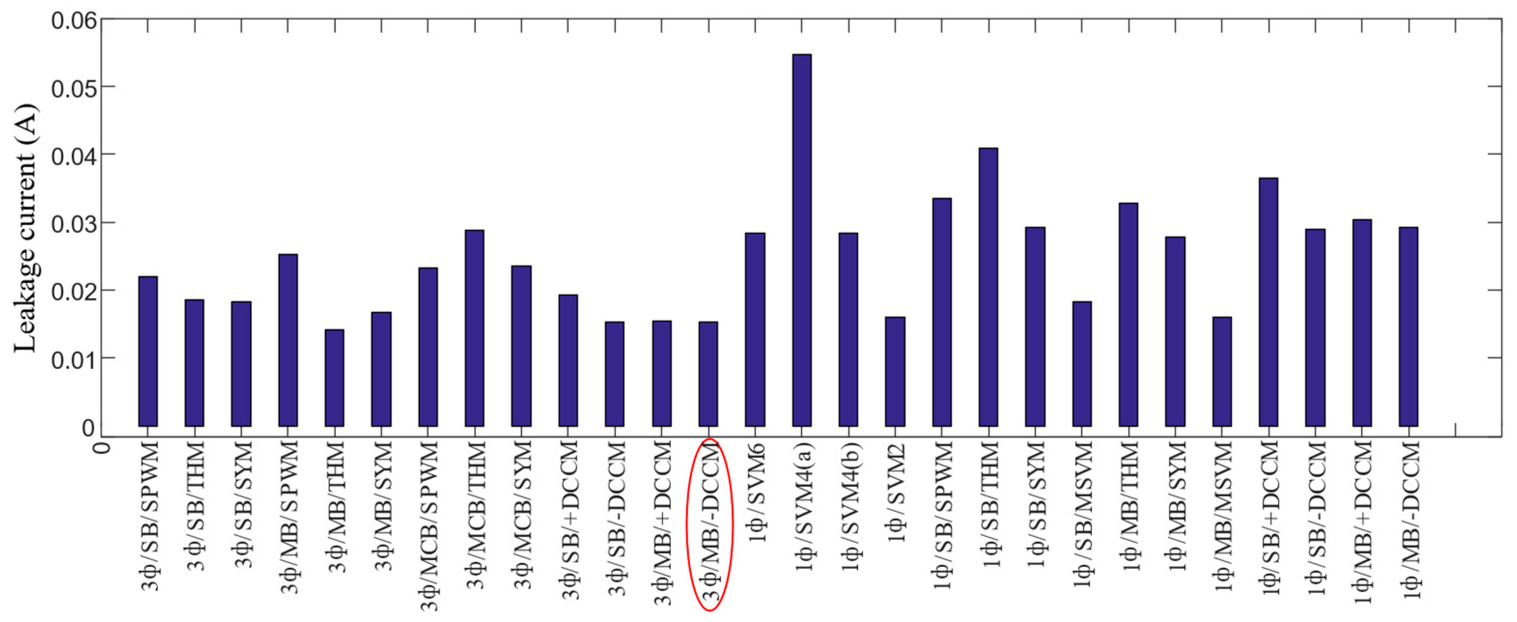
5. Leakage Current Analysis
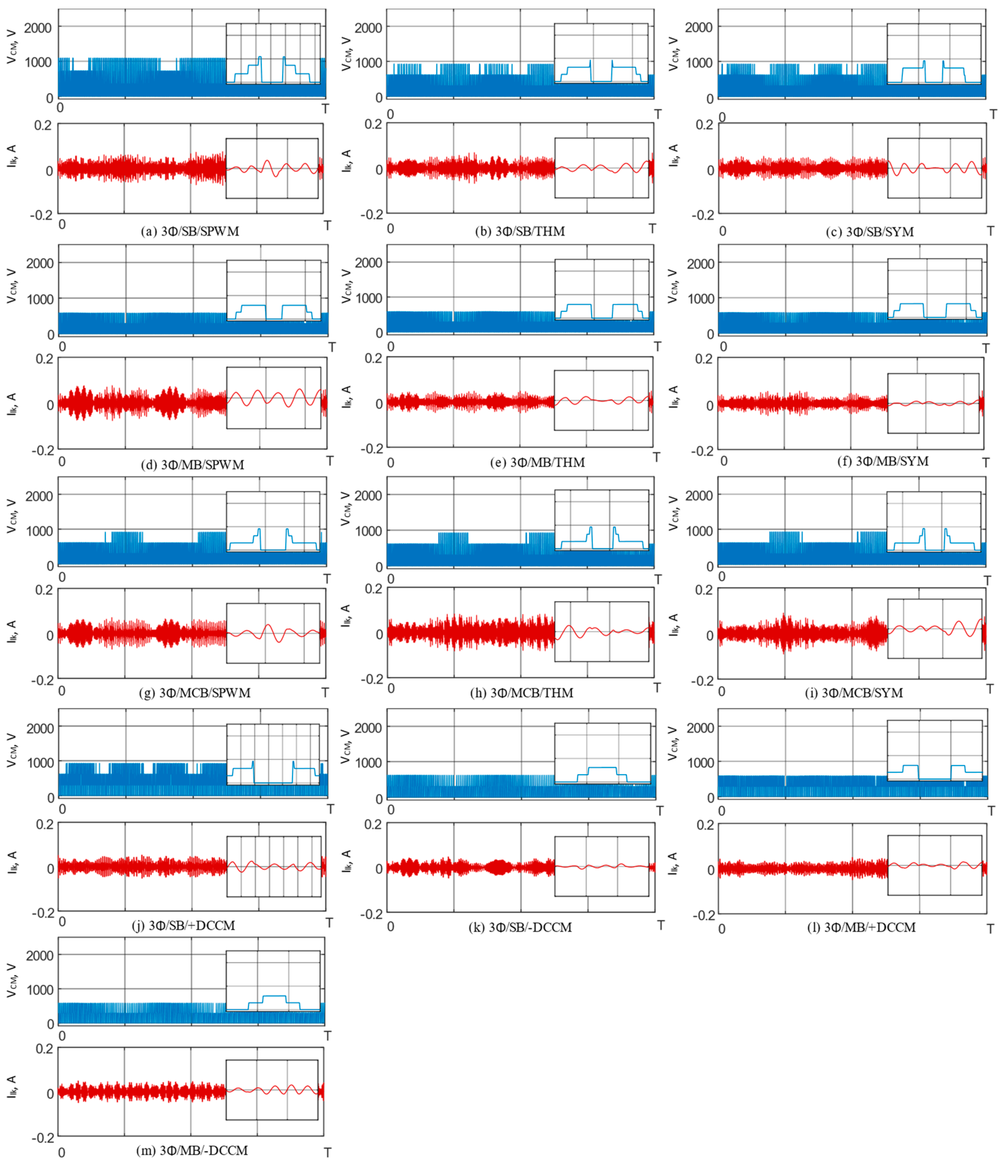
5.1. Three-Phase ST Modulation Techniques
- Both CMV and leakage current in cases of 3Φ/SB/THM and 3Φ/SB/SYM are similar and less than those of 3Φ/SB/SPWM.
- Both 3Φ/MB/SPWM, 3Φ/MB/THM, and 3Φ/MB/SYM have the same value as CMV. On the other hand, the value of leakage current in the case of 3Φ/MB/THM is lower than that of 3Φ/MB/SPWM and 3Φ/MB/SYM.
- The CMV and leakage current value of 3Φ/SB/+DCCM is greater than 3Φ/SB/-DCCM.
- The CMV and the leakage current value of 3Φ/MB/+DCCM are similar and equal to 3Φ/MB/-DCCM.
- Among all the given techniques, 3Φ/MB/-DCCM has the lowest leakage current value in the case of 3Φ ST modulation techniques.
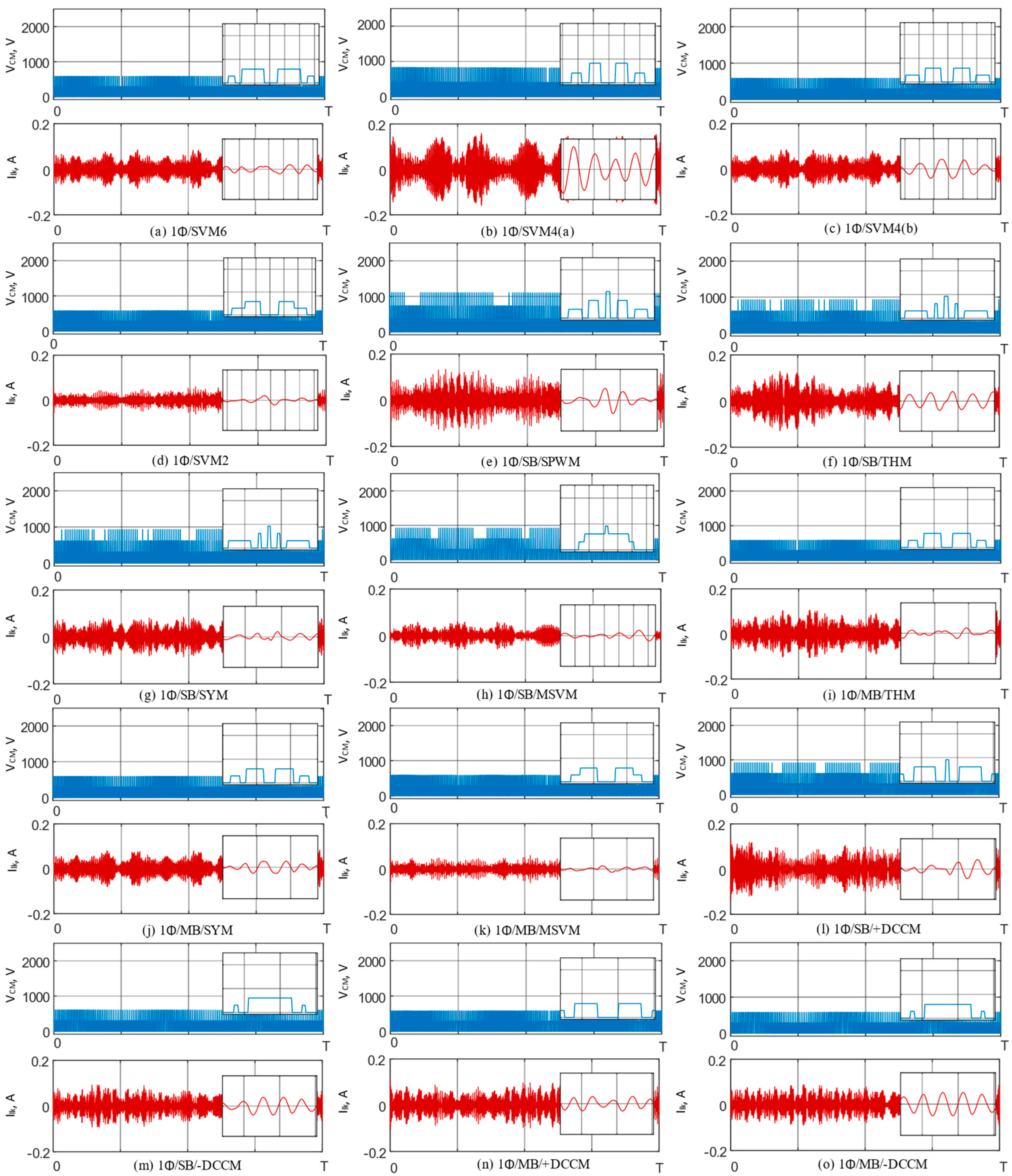
5.2. Single-Phase Shoot-through Modulation Techniques
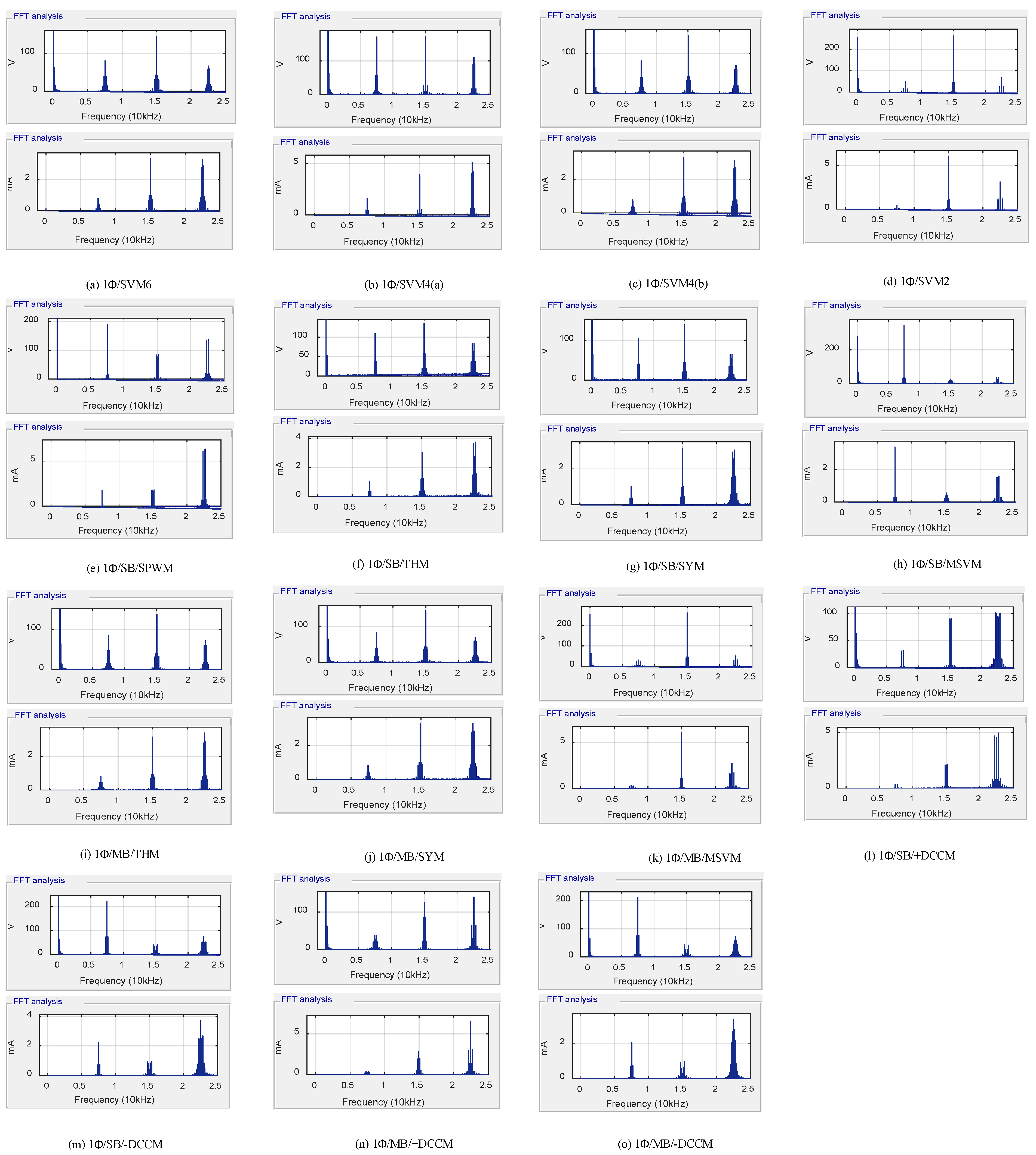
- In the case of SVM schemes, 1Φ/SVM4 (a) has the most considerable value of CMV and leakage current. The lowest value of leakage current is 1Φ/SVM2. The CMV of 1Φ/SB/SPWM is more significant than those of 1Φ/SB/THM, 1Φ/SB/SYM and 1Φ/SB/MSVM. Contrary, the leakage current of 1Φ/SB/MSVM is lower than those of 1Φ/SB/SPWM, 1Φ/SB/THM, and 1Φ/SB/SYM.
- The leakage current of 1Φ/MB/MSVM is lower than 1Φ/MB/THM and 1Φ/MB/SYM.
- The CMV and leakage current of 1Φ/SB/-DCCM is lower than 1Φ/SB/+DCCM.
- Among all the given techniques, 1Φ/SVM2 has the lowest leakage current in 1Φ ST modulation techniques.
6. Spectrum Analysis of QZSI Modulation Techniques
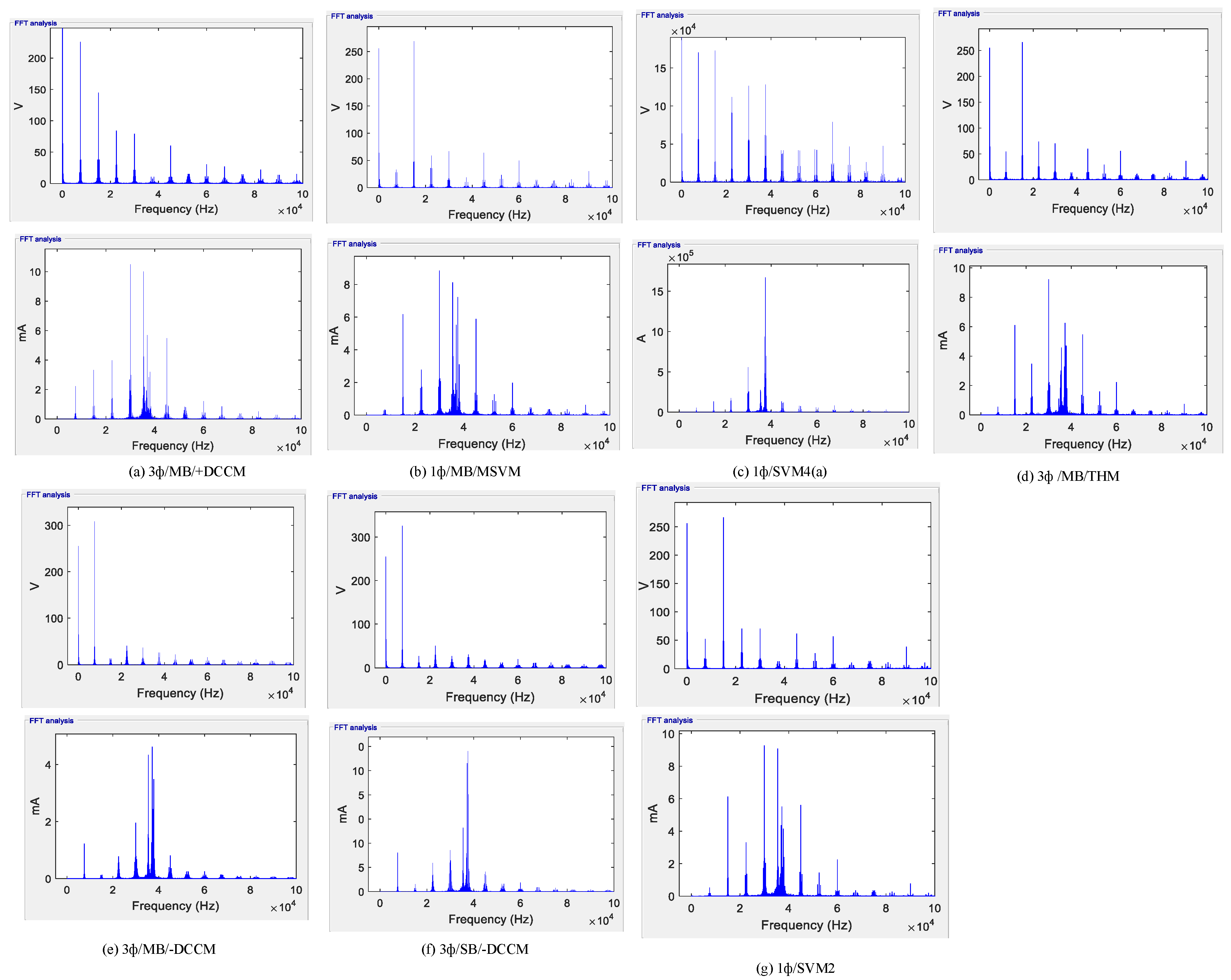
- For 3Φ/SB/THM and 3Φ/SB/SYM spectrum, the CMV and leakage current are similar. This is due to similar waveforms, as discussed later. Further, 3Φ/SB/SPWM has a higher value of CMV and leakage current. For 3Φ/MB/SPWM, 3Φ/MB/THM and 3Φ/MB/SYM spectrum, the CMV and leakage current are similar.
- For 3Φ/MCB/SPWM, 3Φ/MCB/THM, 3Φ/SB/THM and 3Φ/MCB/SYM spectrum, the CMV and leakage current are similar.
- The 3Φ/SB/-DCCM Spectrum has lower CMV and leakage current at . Moreover, harmonic is more petite than 3Φ/SB/+DCCM for the CMV and leakage current.
- For 3Φ/MB/+DCCM Spectrum, the leakage current is higher than 3Φ/MB/-DCCM; this is due to similar waveforms as discussed later. The CMV and leakage current spectrum of 1Φ/SB/SPWM is higher than 1Φ/SB/THM, 1Φ/SB/SYM and 1Φ/SB/MSVM.
- The leakage current spectrum magnitudes of 1Φ/MB/MSVM are lower than 1Φ/MB/SPWM and 1Φ/MB/THM.
7. The Relationship between CMV and Leakage Current
- The low-frequency components of the CMV do not appear on the corresponding leakage current spectrum, while the HF components of the CMV leads to significant leakage current magnitudes at the same frequencies.
- The 3Φ/MB/-DCCM produces the lowest FFT components of the leakage current and CMV compared with the other schemes. This result confirms the previous conclusion from the leakage current magnitude.
8. Simulation Results
8.1. Comparison in Terms of Performance Characteristics
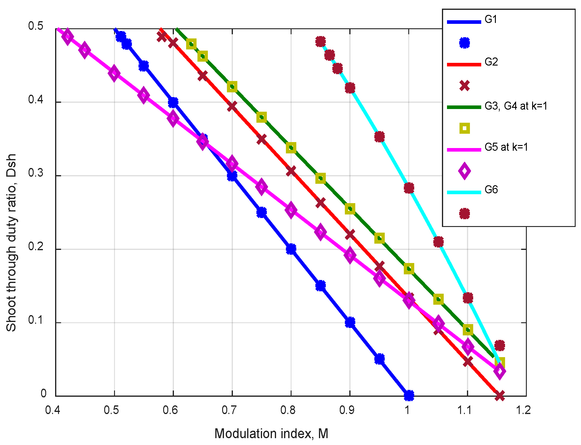
- From Figure 17, 1Φ-ST/SVM4(a) or G5 scheme is the optimal choice because it has a wider operating region.
- From Figure 18, the G6 scheme has the highest values for the ST interval compared with other schemes.
- G6 is the best scheme because it has a higher shoot-through duty ratio and higher boosting action.
- From Figure 19, the G6 scheme is the best with lower values compared with the other scheme for capacitor voltage. G6 is the best scheme because the stress of the capacitor is low, so the capacitor has a low cost and size.
- From Figure 20, the G6 scheme is the best with lower values compared with the other scheme at the same voltage gains for voltage stress.
8.2. Comparison in Terms of CMV Characteristics
8.3. In terms of the Modulation Index
- The minimum value of CMV-RMS results in the minimum value of leakage current.
- From points of view, Figure 22, 1Φ-ST/SVM4(a) or GB7 scheme is the appropriate choice with lower magnitudes when compared to the other schemes in the modulation index range between 0.4 to 0.7. For the modulation index from 0.7 to 1.2, 3Φ/SB/-DCCM and 1Φ/SB/MSVM provide minimum values of when compared with the other scheme. So, the leakage current is low.
8.4. In terms of Voltage Gain
- From Figure 23, for the same voltage gain, it can be observed that CMF3 group has the lowest value of RMS-CMV.
- From Figure 24, for the peak CMV, it is noted that GB3 and GB5. These groups provide minimum values of peak CMV compared with the other scheme.
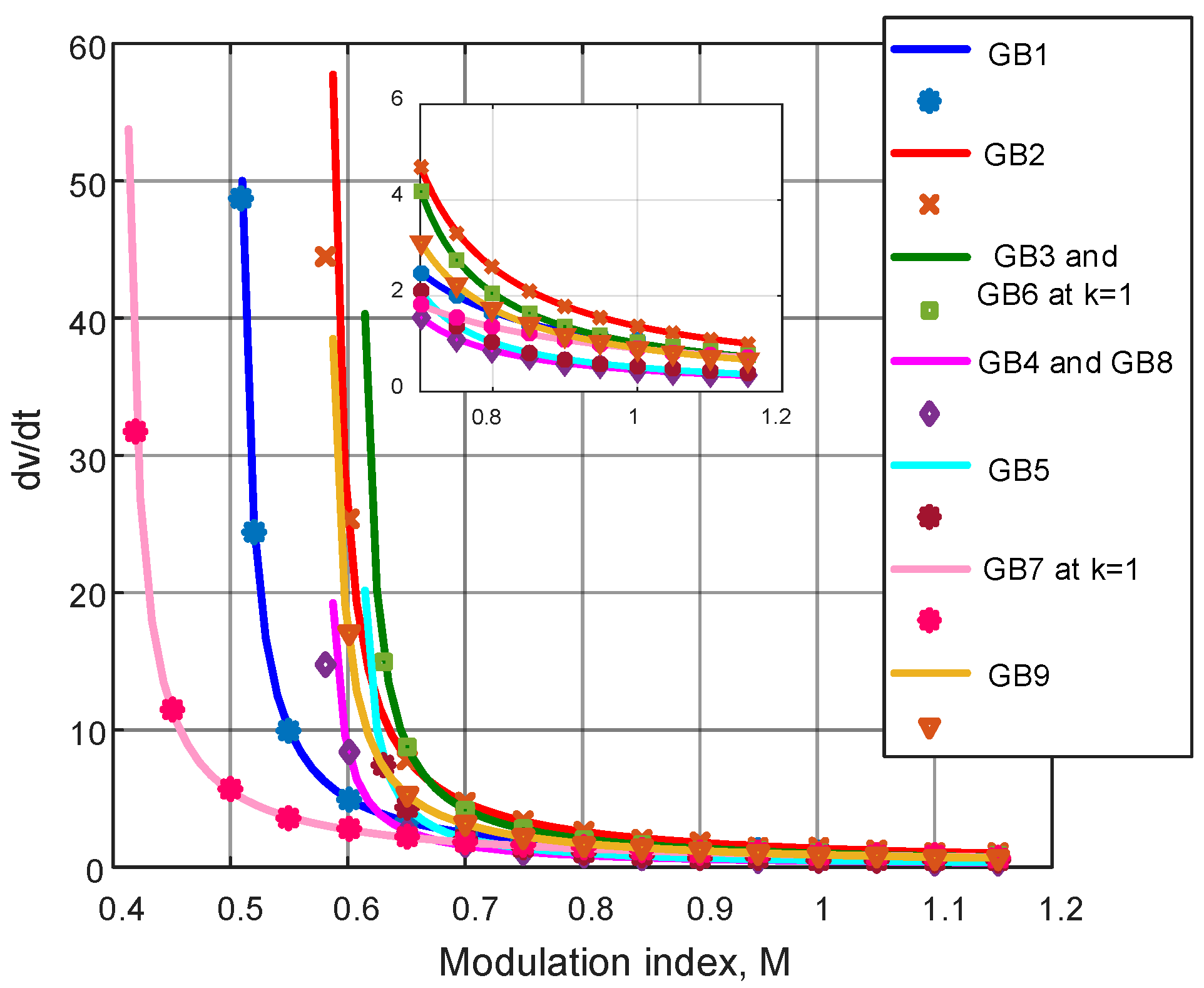
- From Figure 25, for dv/dt, 3Φ/MB/-DCCM scheme provides minimum values compared with the other scheme.
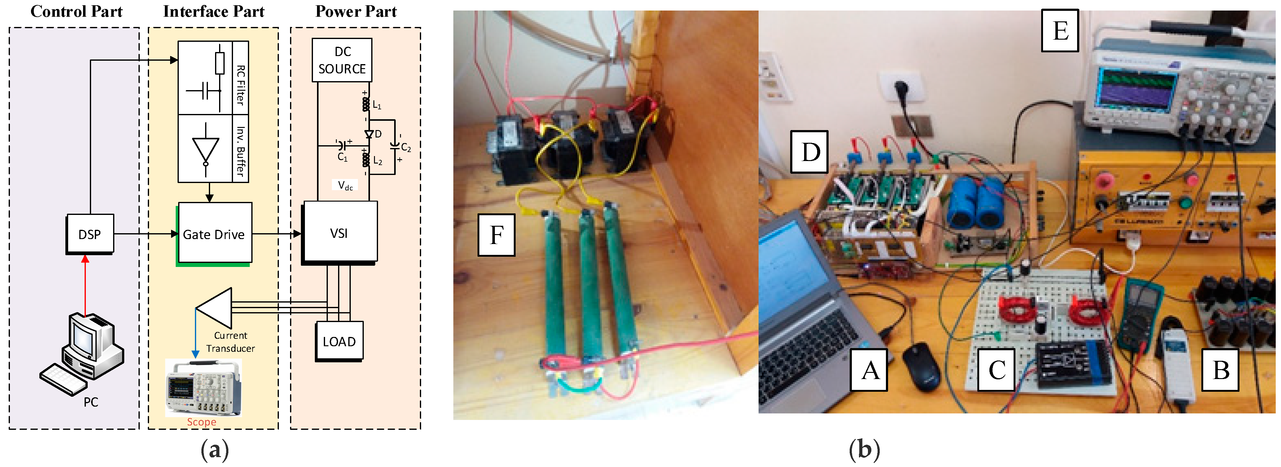
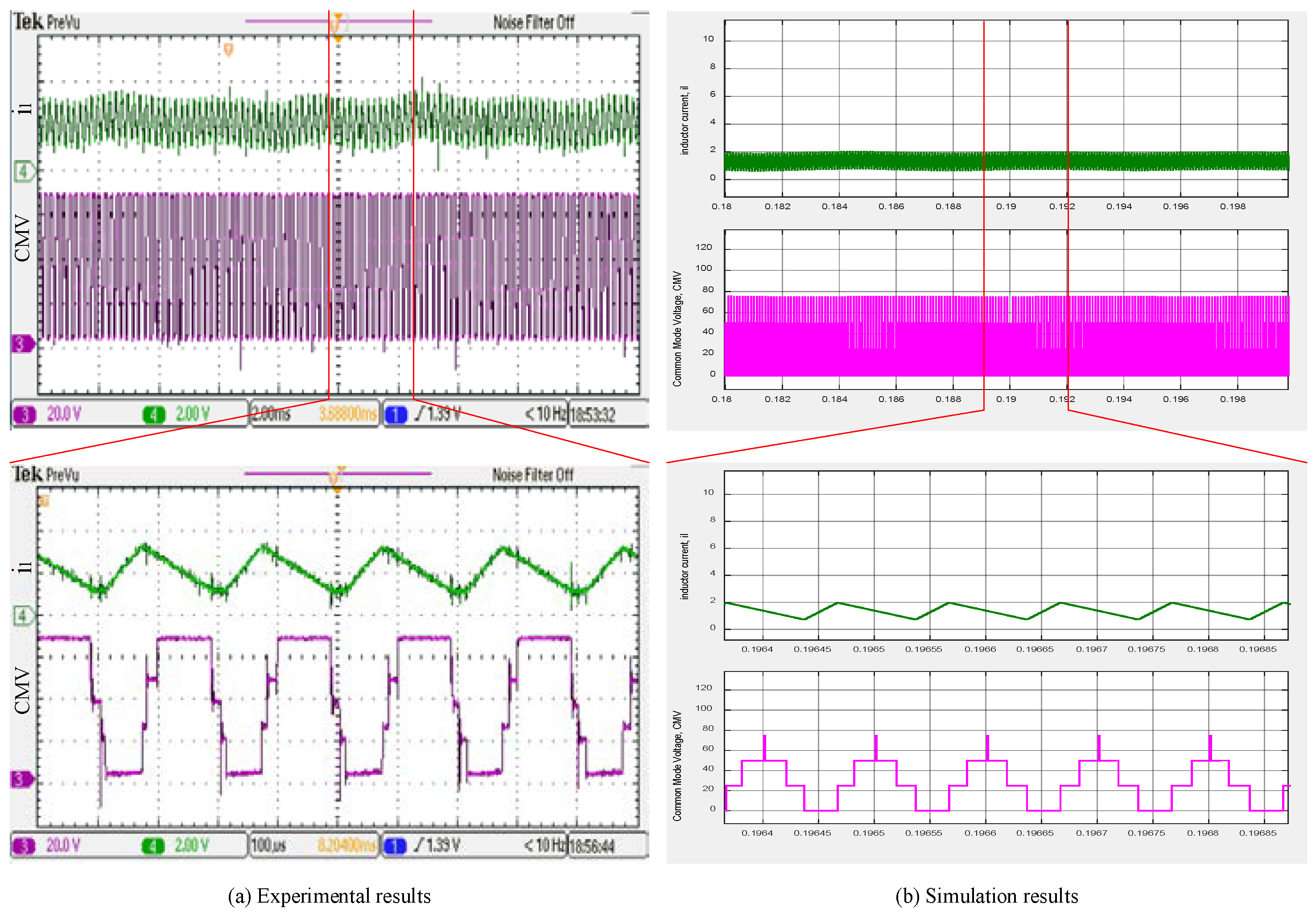
9. Experimental Results
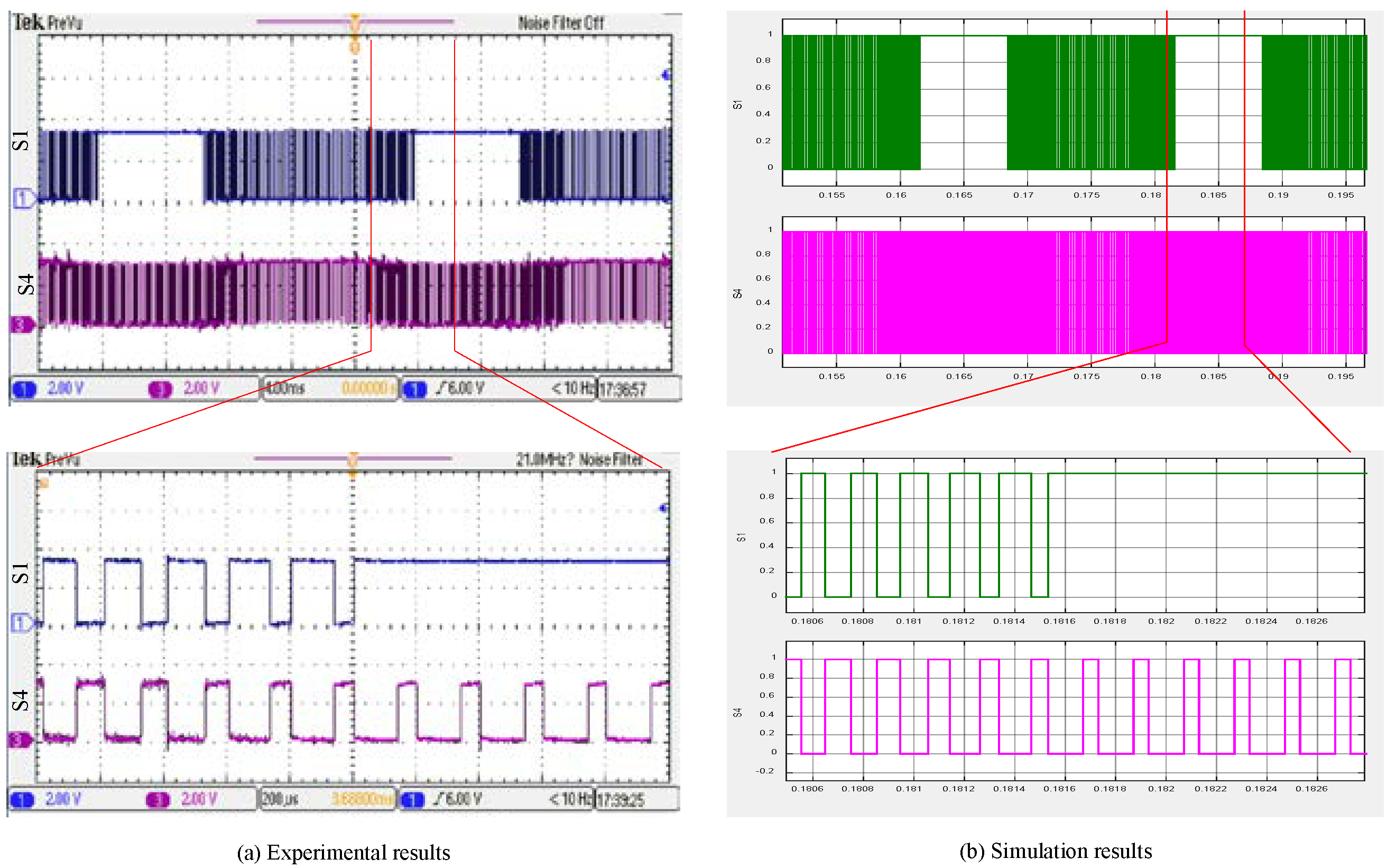
- Figure 27 shows the gating pulses of inverter switches of leg-a. The shown zooming clarifies the periods of non-ST (left half of figure) and ST (right half of the figure). It is noticed that in non-ST, the pulses of two switches are complimentary, while in ST, the ST period is obtained when two switches are on.
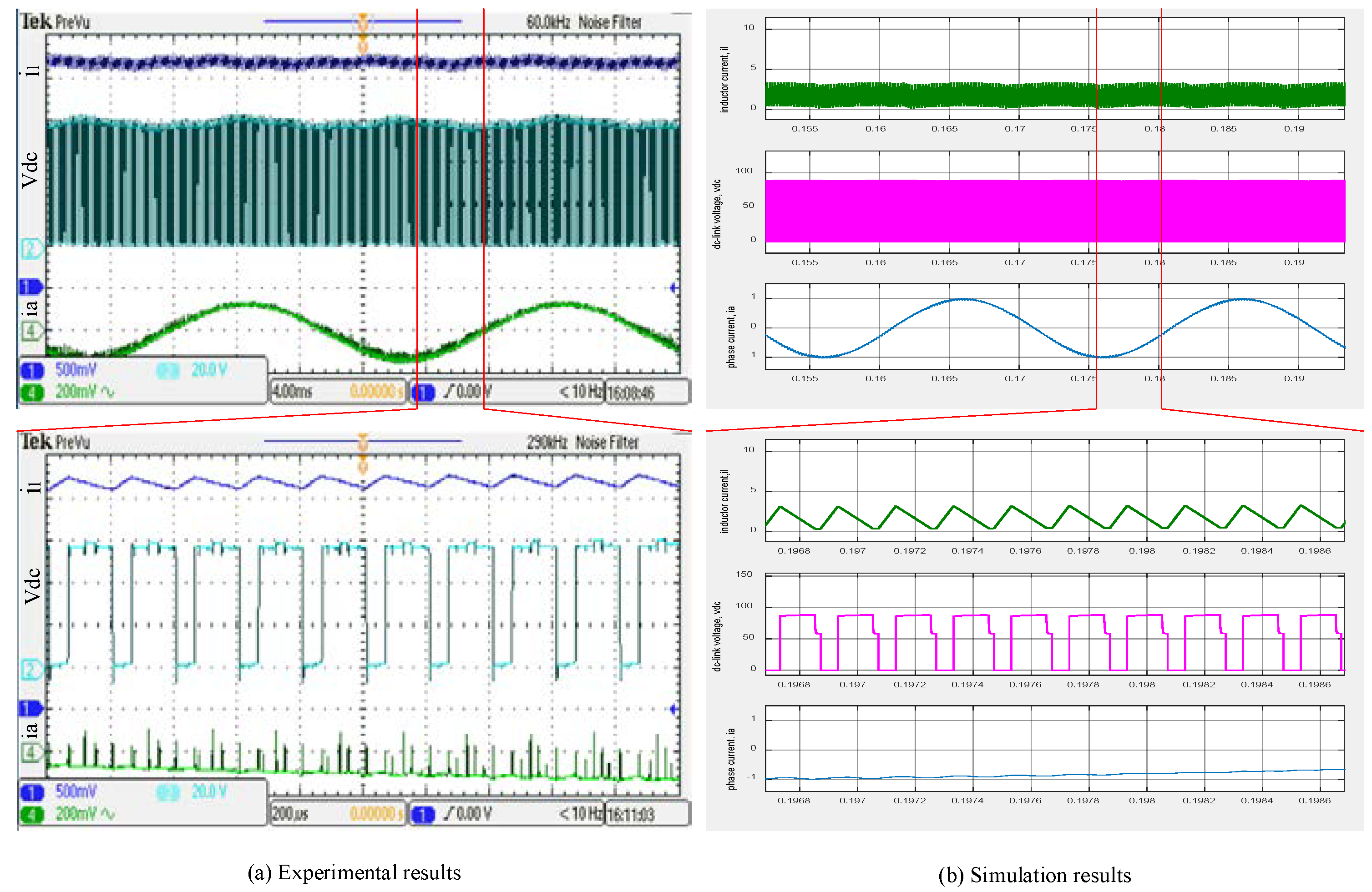
- Figure 28 shows the inductor current and load current ( waveforms.
10. Conclusions
Author Contributions
Funding
Data Availability Statement
Conflicts of Interest
Nomenclature
| VSI | Voltage Source Inverter. |
| ZSI | Impedance (Z-) Source Inverter. |
| QZSI | Quasi-Z Source Inverter. |
| PWM | Pulse Width Modulation. |
| CMV | Common-mode Voltage. |
| RES | Renewable Energy Systems. |
| PV | Photovoltaic. |
| MPPT | Maximum Power Point Tracking. |
| LFTRs | Low-Frequency Transformers. |
| HFTRs | High-Frequency Transformers. |
| IEC | International Electrotechnical Commission. |
| RMS | Root Mean Square. |
| NST | Non-Shoot-Through. |
| ST | Shoot-Through. |
| 3ΦST | Three-leg-ST. |
| 1ΦST | Single-leg-ST. |
| SB | Simple-Boost. |
| MB | Maximum Boost. |
| CB | Constant Boost. |
| SPWM | Sinusoidal PWM. |
| THM | Third Harmonic Modulation. |
| SYM | Symmetrical Modulation. |
| DCCM | DC-Clamped Modulation, it can be + or -. |
| MSVM | Modified Space Vector Modulation. |
| Terminal voltage ate PV modules. | |
| Parasitic Capacitance. | |
| Leakage path resistance. | |
| Impedance network capacitances. | |
| Impedance network inductances. | |
| Forward diode. | |
| DC-link voltage. | |
| Leakage current. | |
| Boosting factor. | |
| Shoot-through duty cycle. | |
| . | |
| Per-phase modulating signal for upper inverter switches. | |
| Per-phase modulating signal for lower inverter switches. | |
| Instantaneous common-mode voltage. | |
| Mean-square Value of common-mode voltage per sub-cycle. |
References
- Verbytskyi, I.; Lukianov, M.; Nassereddine, K.; Pakhaliuk, B.; Husev, O.; Strzelecki, R.M. Power Converter Solutions for Industrial PV Applications—A Review. Energies 2022, 15, 3295. [Google Scholar] [CrossRef]
- Duong, T.-D.; Nguyen, M.-K.; Tran, T.-T.; Vo, D.-V.; Lim, Y.-C.; Choi, J.-H. Topology Review of Three-Phase Two-Level Transformerless Photovoltaic Inverters for Common-Mode Voltage Reduction. Energies 2022, 15, 3106. [Google Scholar] [CrossRef]
- Jäger-Waldau, A. Snapshot of photovoltaics—February 2022. EPJ Photovolt. 2022, 13, 9. [Google Scholar] [CrossRef]
- Jäger-Waldau, A. Snapshot of Photovoltaics—February 2020. Energies 2020, 13, 930. [Google Scholar] [CrossRef] [Green Version]
- Nordrum, A. At last, a massive solar park for Egypt: A 1.8-GW, $4 billion solar power plant is coming on line in the Sahara—[News]. IEEE Spectr. 2019, 56, 8–9. [Google Scholar] [CrossRef]
- Renewable Energy World. IHS Markit Releases New 2020 Solar Installation Forecast in Light of the Impact of COVID-19. Available online: https://www.renewableenergyworld.com/solar/ihs-markit-releases-new-2020-solar-installation-forecast-in-light-of-the-impact-of-covid-19/#gref (accessed on 21 August 2021).
- BloombergNEF. Report Archives. Available online: https://about.bnef.com/blog/category/report/ (accessed on 21 August 2021).
- IRENA, Renewable Energy Outlook: Egypt. 2018. Available online: https://www.irena.org/publications/2018/oct/renewable-energy-outlook-egypt (accessed on 8 October 2018).
- New & Renewable Energy Authority Egypt. Strategic Environmental & Social Assessment Final Report. February 2016, pp. 1–220. Available online: https://www.eib.org/attachments/registers/65771943.pdf (accessed on 12 October 2018).
- Van Wyk, J.D.; Lee, F.C. On a Future for Power Electronics. IEEE J. Emerg. Sel. Top. Power Electron. 2013, 1, 59–72. [Google Scholar] [CrossRef]
- Kjaer, S.; Pedersen, J.; Blaabjerg, F. A Review of Single-Phase Grid-Connected Inverters for Photovoltaic Modules. IEEE Trans. Ind. Appl. 2005, 41, 1292–1306. [Google Scholar] [CrossRef]
- ElNozahy, M.S.; Salama, M.M.A. Technical impacts of grid-connected photovoltaic systems on electrical networks—A review. J. Renew. Sustain. Energy 2013, 5, 032702. [Google Scholar] [CrossRef]
- Ma, T.-T. Power quality enhancement in micro-grids using multifunctional DG, inverters Title. In Proceedings of the International MultiConference of Engineers and Computer Scientists, Hong Kong, 14–16 March 2012; Volume 2, pp. 14–16. [Google Scholar]
- Hizam, H.; Aris, I.; Kadir, M.; Akorede, M. A Critical Review of Strategies for Optimal Allocation of Distributed Generations Units in Electrical Power Systems. Int. Rev. Electr. Eng. 2010, 5, 593–600. [Google Scholar]
- Romero, E.; Francois, B.; Malinowski, M.; Zhong, Q. Grid-Connected Photovoltaic Plants: An Alternative Energy Source, Replacing Conventional Sources. IEEE Ind. Electron. Mag. 2015, 9, 18–32. [Google Scholar] [CrossRef]
- Rampinelli, G.A.; Gasparin, F.P.; Bühler, A.J.; Krenzinger, A.; Romero, F.C. Assessment and mathematical modeling of energy quality parameters of grid connected photovoltaic inverters. Renew. Sustain. Energy Rev. 2015, 52, 133–141. [Google Scholar] [CrossRef]
- Ikkurti, H.P.; Saha, S. A comprehensive techno-economic review of microinverters for Building Integrated Photovoltaics (BIPV). Renew. Sustain. Energy Rev. 2015, 47, 997–1006. [Google Scholar] [CrossRef]
- Kouro, S.; Leon, J.I.; Vinnikov, D.; Franquelo, L.G. Grid-connected photovoltaic systems: An overview of recent research and emerging PV converter technology. IEEE Ind. Electron. Mag. 2015, 9, 47–61. [Google Scholar] [CrossRef]
- Alluhaybi, K.; Batarseh, I.; Hu, H. Comprehensive Review and Comparison of Single-Phase Grid-Tied Photovoltaic Microinverters. IEEE J. Emerg. Sel. Top. Power Electron. 2020, 8, 1310–1329. [Google Scholar] [CrossRef]
- Teodorescu, R.; Liserre, M.; Rodríguez, P. Chapter 10: Control of grid converters under grid faults. In Grid Converters for Photovoltaic and Wind Power Systems, 1st ed.; Wiley and Sons Publications: Chicheter, UK, 2011; Volume 1, pp. 237–289. [Google Scholar]
- Carrasco, J.M.; Franquelo, L.G.; Bialasiewicz, J.T.; Galvan, E.; PortilloGuisado, R.; Prats, M.A.M.; Leon, J.I.; Moreno-Alfonso, N. Power-electronic systems for the grid integration of renewable energy sources: A survey. IEEE Trans. Ind. Electron. 2004, 53, 1002–1016. [Google Scholar] [CrossRef]
- Gonzalez, R.; Gubia, E.; Lopez, J.; Marroyo, L. Transformerless Single-Phase Multilevel-Based Photovoltaic Inverter. IEEE Trans. Ind. Electron. 2008, 55, 2694–2702. [Google Scholar] [CrossRef]
- Wu, W.; Sun, Y.; Lin, Z.; Tang, T.; Blaabjerg, F.; Chung, H.S.-H. A New LCL-Filter with In-Series Parallel Resonant Circuit for Single-Phase Grid-Tied Inverter. IEEE Trans. Ind. Electron. 2013, 61, 4640–4644. [Google Scholar] [CrossRef]
- Meneses, D.; Blaabjerg, F.; García, O.; Cobos, J.A. Review and Comparison of Step-Up Transformerless Topologies for Photovoltaic AC-Module Application. IEEE Trans. Power Electron. 2013, 28, 2649–2663. [Google Scholar] [CrossRef] [Green Version]
- Patrao, I.; Figueres, E.; González-Espín, F.; Garcerá, G. Transformerless topologies for grid-connected single-phase photovoltaic inverters. Renew. Sustain. Energy Rev. 2011, 15, 3423–3431. [Google Scholar] [CrossRef] [Green Version]
- Latran, M.B.; Teke, A. Investigation of multilevel multifunctional grid connected inverter topologies and control strategies used in photovoltaic systems. Renew. Sustain. Energy Rev. 2015, 42, 361–376. [Google Scholar] [CrossRef]
- Hasan, R.; Mekhilef, S.; Seyedmahmoudian, M.; Horan, B. Grid-connected isolated PV microinverters: A review. Renew. Sustain. Energy Rev. 2016, 67, 1065–1080. [Google Scholar] [CrossRef]
- Rampinelli, G.; Krenzinger, A.; Romero, F.C. Mathematical models for efficiency of inverters used in grid connected photovoltaic systems. Renew. Sustain. Energy Rev. 2014, 34, 578–587. [Google Scholar] [CrossRef]
- Cavalcanti, M.C.; de Oliveira, K.C.; Neves, F.A.S.; Azevedo, G.M.S.; Camboim, F.C. Modulation Techniques to Eliminate Leakage Currents in Transformerless Three-Phase Photovoltaic Systems. IEEE Trans. Ind. Electron. 2009, 57, 1360–1368. [Google Scholar] [CrossRef]
- Gubía, E.; Sanchis, P.; Ursúa, A.; López, J.; Marroyo, L. Ground currents in single-phase transformerless photovoltaic systems. Prog. Photovolt. Res. Appl. 2007, 15, 629–650. [Google Scholar] [CrossRef]
- Cavalcanti, M.C.; Farias, A.M.; Oliveira, K.C.; Neves, F.A.S.; Afonso, J.L. Eliminating Leakage Currents in Neutral Point Clamped Inverters for Photovoltaic Systems. IEEE Trans. Ind. Electron. 2011, 59, 435–443. [Google Scholar] [CrossRef]
- López, Ó.; Freijedo, F.D.; Yepes, A.G.; Fernández-Comesaña, P.; Malvar, J.; Teodorescu, R.; Doval-Gandoy, J. Eliminating Ground Current in a Transformerless Photovoltaic Application. IEEE Trans. Energy Convers. 2010, 25, 140–147. [Google Scholar] [CrossRef]
- Lee, J.-S.; Lee, K.-B. New Modulation Techniques for a Leakage Current Reduction and a Neutral-Point Voltage Balance in Transformerless Photovoltaic Systems Using a Three-Level Inverter. IEEE Trans. Power Electron. 2013, 29, 1720–1732. [Google Scholar] [CrossRef]
- Cha, W.; Kim, K.; Cho, Y.; Lee, S.; Kwon, B. Evaluation and analysis of transformerless photovoltaic inverter topology for efficiency improvement and reduction of leakage current. IET Power Electron. 2015, 8, 255–267. [Google Scholar] [CrossRef]
- Yang, B.; Li, W.; Gu, Y.; Cui, W.; He, X. Improved Transformerless Inverter with Common-Mode Leakage Current Elimination for a Photovoltaic Grid-Connected Power System. IEEE Trans. Power Electron. 2011, 27, 752–762. [Google Scholar] [CrossRef]
- Hou, C.-C.; Shih, C.-C.; Cheng, P.-T.; Hava, A.M. Common-Mode Voltage Reduction Pulsewidth Modulation Techniques for Three-Phase Grid-Connected Converters. IEEE Trans. Power Electron. 2012, 28, 1971–1979. [Google Scholar] [CrossRef]
- Peng, F.Z. Z-Source Inverter. IEEE Trans. Ind. Appl. 2003, 39, 504–510. [Google Scholar] [CrossRef]
- Peng, F.Z.; Yuan, X.; Fang, X.; Qian, Z. Z-source inverter for adjustable speed drives. IEEE Power Electron. Lett. 2003, 1, 33–35. [Google Scholar] [CrossRef]
- Jamal, I.; Elmorshedy, M.F.; Dabour, S.M.; Rashad, E.M.; Almakhles, D.J.; Xu, W. A Comprehensive Review of Grid-Connected PV Systems Based on Impedance Source Inverter. IEEE Access 2022, 10, 89101–89123. [Google Scholar] [CrossRef]
- Li, Y.; Jiang, S.; Cintron-Rivera, J.G.; Peng, F.Z. Modeling and Control of Quasi-Z-Source Inverter for Distributed Generation Applications. IEEE Trans. Ind. Electron. 2012, 60, 1532–1541. [Google Scholar] [CrossRef]
- Ge, B.; Abu-Rub, H.; Peng, F.Z.; Lei, Q.; de Almeida, A.T.; Ferreira, F.J.T.E.; Sun, D.; Liu, Y. An Energy-Stored Quasi-Z-Source Inverter for Application to Photovoltaic Power System. IEEE Trans. Ind. Electron. 2013, 60, 4468–4481. [Google Scholar] [CrossRef]
- Freddy, T.K.S.; Rahim, N.A.; Hew, W.-P.; Che, H.S. Modulation Techniques to Reduce Leakage Current in Three-Phase Transformerless H7 Photovoltaic Inverter. IEEE Trans. Ind. Electron. 2014, 62, 322–331. [Google Scholar] [CrossRef]
- Morris, C.T.; Han, D.; Sarlioglu, B. Reduction of Common Mode Voltage and Conducted EMI Through Three-Phase Inverter Topology. IEEE Trans. Power Electron. 2016, 32, 1720–1724. [Google Scholar] [CrossRef]
- Dabour, S.M.; Abdel-Wahab, S.M.; Rashad, E.M. Common-Mode Voltage Reduction Algorithm with Minimum Switching Losses for Three-Phase Inverters. In Proceedings of the 2019 21st International Middle East Power Systems Conference (MEPCON), Cairo, Egypt, 17–19 December 2019; pp. 1210–1215. [Google Scholar]
- Hou, C.-C.; Shih, C.-C.; Chengt, P.-T.; Hava, A.M. Common-Mode Voltage Reduction Modulation Techniques for three-Phase Grid Connected Converters. In Proceedings of the 2010 International Power Electronics Conf. ECCE ASIA, Sapporo, Japan, 22–24 June 2010; pp. 1125–1131. [Google Scholar]
- Liu, Y.; Ge, B.; Abu-Rub, H.; Peng, F.Z. Overview of Space Vector Modulations for Three-Phase Z-Source/Quasi-Z-Source Inverters. IEEE Trans. Power Electron. 2013, 29, 2098–2108. [Google Scholar] [CrossRef]
- Ellabban, O.; Van Mierlo, J.; Lataire, P. Comparison between different PWM control methods for different Z-source inverter topologies. In Proceedings of the 2009 13th European Conference on Power Electronics and Applications, Barcelona, Spain, 8–10 September 2009; pp. 1–11. [Google Scholar]
- Abdelhakim, A.; Blaabjerg, F.; Mattavelli, P. Modulation Schemes of the Three-Phase Impedance Source Inverters—Part I: Classification and Review. IEEE Trans. Ind. Electron. 2018, 65, 6309–6320. [Google Scholar] [CrossRef]
- Abdelhakim, A.; Blaabjerg, F.; Mattavelli, P. Modulation Schemes of the Three-Phase Impedance Source Inverters—Part II: Comparative Assessment. IEEE Trans. Ind. Electron. 2018, 65, 6321–6332. [Google Scholar] [CrossRef]
- Siwakoti, Y.P.; Peng, F.Z.; Blaabjerg, F.; Loh, P.C.; Town, G.E.; Yang, S. Impedance-Source Networks for Electric Power Conversion Part II: Review of Control and Modulation Techniques. IEEE Trans. Power Electron. 2014, 30, 1887–1906. [Google Scholar] [CrossRef]
- Siwakoti, Y.P.; Town, G.E. Three-Phase Transformerless Grid Connected Quasi Z-Source Inverter for Solar Photovoltaic Systems with Minimal Leakage Current. In Proceedings of the 3rd IEEE International Symposium on Power Electronics for Distributed Generation Systems, Aalborg, Denmark, 25–28 June 2012; pp. 368–373. [Google Scholar]
- Noroozi, N.; Zolghadri, M.R.; Yaghoubi, M. Comparison of Common-Mode Voltage in Three-Phase Quasi-Z-Source Inverters Using Different Shoot-Through Implementation Methods. In Proceedings of the 2018 IEEE 12th International Conference on Compatibility, Power Electronics and Power Engineering, CPE-POWERENG, Doha, Qatar, 10–12 April 2018; pp. 1–6. [Google Scholar]
- Noroozi, N.; Zolghadri, M.R. Three-Phase Quasi-Z-Source Inverter with Constant Common-Mode Voltage for Photovoltaic Application. IEEE Trans. Ind. Electron. 2017, 65, 4790–4798. [Google Scholar] [CrossRef]
- Liu, W.; Yang, Y.; Kerekes, T.; Liivik, E.; Vinnikov, D.; Blaabjerg, F. Common-Mode Voltage Analysis and Reduction for the Quasi-Z-Source Inverter with a Split Inductor. Appl. Sci. 2020, 10, 8713. [Google Scholar] [CrossRef]
- El-Hendawy, N.; Dabour, S.M.; Rashad, E.M. Common-Mode Voltage Analysis of Three-phase Quasi-Z Source Inverters for Transformerless Photovoltaic Systems. In Proceedings of the 2019 IEEE Conference on Power Electronics and Renewable Energy (CPERE), Aswan, Egypt, 23–25 October 2019; pp. 355–360. [Google Scholar]


| 3Φ-ST Modulation Techniques | 1Φ-ST Modulation Techniques | |||||||||||
|---|---|---|---|---|---|---|---|---|---|---|---|---|
| Technique | 3Φ/SB/SPWM | 3Φ/SB/THM 3Φ/SB/SYM | 3Φ/MB/SPWM 3Φ/MB/THM 3Φ/MB/SYM | 3Φ/MCB/SPWM 3Φ/MCB/THM 3Φ/MCB/SYM 3Φ/SB/+DCCM 3Φ/SB/-DCCM | 3Φ/MB/+DCCM 3Φ/MB/-DCCM | 1Φ/SVM6 1Φ/SVM4(b) 1Φ/SVM2 | 1Φ/SVM4(a) | 1Φ/SB/SPWM | 1Φ/SB/THM 1Φ/SB/SYM 1Φ/SB/MSVM | 1Φ/MB/THM 1Φ/MB/SYM 1Φ/MB/MSVM | 1Φ/SB/-DCCM 1Φ/SB/+DCCM | 1Φ/MB/+DCCM 1Φ/MB/-DCCM |
| B | ||||||||||||
| G | ||||||||||||
| Group | G1 | G2 | G3 | G2 | G3 | G4 | G5 | G1 | G2 | G3 | G2 | G3 |
| State | ||
|---|---|---|
| {100}, {010}, {001} | ||
| Even ( | {110}, {011}, {101} | |
| Zero-state ( | {000} | 0 |
| Zero-state ( | {111} | |
| - | 0 | |
| 3Φ-ST Modulation Techniques | 1Φ-ST Modulation Techniques | |||||||||
|---|---|---|---|---|---|---|---|---|---|---|
| Technique | 3Φ/SB/SPWM | 3Φ/SB/THM 3Φ/SB/SYM 3Φ/MCB/SPWM 3Φ/MCB/THM 3Φ/MCB/SYM | 3Φ/MB/SPWM 3Φ/MB/THM 3Φ/MB/SYM 3Φ/SB/-DCCM 3Φ/MB/+DCCM 3Φ/MB/-DCCM | 3Φ/SB/+DCCM | 1Φ/SVM6 1Φ/SVM4(a) 1Φ/SVM2 | 1Φ/SVM4(b) | 1Φ/SB/SPWM | 1Φ/SB/THM 1Φ/SB/SYM | 1Φ/MB/THM 1Φ/MB/SYM 1Φ/MB/MSVM 1Φ/SB/-DCCM 1Φ/MB/+DCCM 1Φ/MB/-DCCM | 1Φ/SB/MSVM 1Φ/SB/+DCCM |
| MS Value | ||||||||||
| Group | CMF1 | CMF2 | CMF3 | CMF4 | CMF5 | CMF6 | CMF1 | CMF2 | CMF3 | CMF4 |
| 3Φ-ST Modulation Techniques | 1Φ-ST Modulation Techniques | ||||||||||||
|---|---|---|---|---|---|---|---|---|---|---|---|---|---|
| Technique | SB/SPWM | SB/THM SB/SYM MCB/SPWM MCB/THM MCB/SYM SB/+DCCM | MB/SPWM MB/THM MB/SYM MB/+DCCM MB/+DCCM | SB/-DCCM | MB/-DCCM | SVM6 SVM4(b) SVM2 | SVM4(a) | SB/SPWM | SB/THM SB/SYM | SB/MSVM | MB/THM MB/SYM MB/MSVM MB/+DCCM MB/-DCCM | SB/+DCCM | SB/-DCCM |
| Peak CMV | |||||||||||||
| Groups | GB1 | GB2 | GB3 | GB4 | GB5 | GB6 | GB7 | GB1 | GB2 | GB8 | GB3 | GB2 | GB9 |
| Parameter | Value | Parameter | Value |
|---|---|---|---|
| Input voltage | 150 V | Output frequency | 50 Hz |
| Switching frequency | 7.5 kHz | ||
| Z-network components | |||
| Inductances | mH | Capacitances | F |
| Load parameters | |||
| Resistance | 10 Ω | Inductance | 50 mH |
| Group (Method) | G1 | G2 | G3 | G4 | G5 |
|---|---|---|---|---|---|
| Parameter | Value | Parameter | Value |
|---|---|---|---|
| Source voltage (E) | 30 V | Output frequency (f) | 50 Hz |
| Z-inductance (L) | 1.25 mH | 5 kHz | |
| Z-capacitance (C) | F | Modulation index (M) | 0.8 |
| 2 × 10⁻⁴ | Inductive load (R+L) | 11 Ω + 5 mH | |
| Voltage gain (G) | 3 | 90 V |
Disclaimer/Publisher’s Note: The statements, opinions and data contained in all publications are solely those of the individual author(s) and contributor(s) and not of MDPI and/or the editor(s). MDPI and/or the editor(s) disclaim responsibility for any injury to people or property resulting from any ideas, methods, instructions or products referred to in the content. |
© 2022 by the authors. Licensee MDPI, Basel, Switzerland. This article is an open access article distributed under the terms and conditions of the Creative Commons Attribution (CC BY) license (https://creativecommons.org/licenses/by/4.0/).
Share and Cite
Dabour, S.M.; El-hendawy, N.; Aboushady, A.A.; Farrag, M.E.; Rashad, E.M. A Comprehensive Review on Common-Mode Voltage of Three-Phase Quasi-Z Source Inverters for Photovoltaic Applications. Energies 2023, 16, 269. https://doi.org/10.3390/en16010269
Dabour SM, El-hendawy N, Aboushady AA, Farrag ME, Rashad EM. A Comprehensive Review on Common-Mode Voltage of Three-Phase Quasi-Z Source Inverters for Photovoltaic Applications. Energies. 2023; 16(1):269. https://doi.org/10.3390/en16010269
Chicago/Turabian StyleDabour, Sherif M., Noha El-hendawy, Ahmed A. Aboushady, Mohamed Emad Farrag, and Essam M. Rashad. 2023. "A Comprehensive Review on Common-Mode Voltage of Three-Phase Quasi-Z Source Inverters for Photovoltaic Applications" Energies 16, no. 1: 269. https://doi.org/10.3390/en16010269
APA StyleDabour, S. M., El-hendawy, N., Aboushady, A. A., Farrag, M. E., & Rashad, E. M. (2023). A Comprehensive Review on Common-Mode Voltage of Three-Phase Quasi-Z Source Inverters for Photovoltaic Applications. Energies, 16(1), 269. https://doi.org/10.3390/en16010269