Article

Improving the Efficiency of the Shunt Active Power Filter Acting with the Use of the Hysteresis Current Control Technique

Faculty of Electrical and Computer Engineering, Cracow University of Technology, 31-155 Cracow, Poland
Energies 2023, 16(10), 4080; https://doi.org/10.3390/en16104080
Submission received: 8 April 2023 / Revised: 1 May 2023 / Accepted: 6 May 2023 / Published: 13 May 2023

Abstract

:
Calculation of the reference waveform for the compensating current generated by the shunt active power filter (ShAPF) can be carried out using various methods. In this article, this calculation is performed indirectly on the basis of tracking and processing of the ShAPF DC-link capacitor voltage. At the same time, the energy stored in this capacitor is used to generate the compensating current. Therefore, the operation of this capacitor during compensation, i.e., changes in energy stored in it and the voltage waveform on its terminals, is characteristic and crucial for the method considered. Once the current reference waveform is determined, it can be generated by ShAPF in various ways, but always using the energy stored in the DC-link capacitor. The power module of the active filter uses transistor switches to realize the required compensating current. During their operation, power losses occur that can be divided into either switching or conduction. The article shows that, in the case of the indirect control method and the hysteresis current control technique used, it is possible to reduce the operating frequency of the switches and the load on the DC-link capacitor. Thanks to this, it is possible to reduce power losses in these elements and extend their lifetime.

1. Introduction

Electricity should be delivered from the places of its generation to the places of its consumption at required voltage and reasonable cost [1]. These issues, covering a wide scope of theory and practice in electrical engineering, create an area of knowledge called power quality. Systematization of issues related to power quality can be found, e.g., in [1].
A widespread regularity is that the increase in load power and the expanding complicated nature of electric devices deteriorate the operating conditions of the grid, both in the technical and economic sense [2,3], especially now when there is a massive increase in renewable sources for power systems [4,5].
Accommodating the appropriate quality of power can be performed in two ways: with the use of devices of high quality and efficiency of electricity conversion or with the use of devices that can mitigate the negative impact of disturbing loads on supply systems.
The first way can be carried out with electrical devices that, if possible, are constructed to be linear, symmetrical, and time invariant, or restructure them (redesign into a power electronic device with the same functional purpose) to appear linear, balanced, and time invariant. As the examples that can be considered classical, there are devices designed and controlled with the use of the power factor correction (PFC) technique [6,7,8,9] or a study on the high-quality power conversion with the use of matrix converters [10].
The second way to improve power quality can be carried out by means of active filters, a class of power electronic devices which, being separate devices from the loads, compensate for the negative impact of the loads on the grid or improve the distorted grid voltage to the required quality. General possibilities of using active filters to improve power quality are presented in [11,12,13,14].
Power delivery entails voltage drops and energy losses along the transmission line. These phenomena are all the more significant, the greater the rms of the supply current over the rms of the current resulting from the active power of the supplied load. Power electronics can actively reduce the rms of the supply current by compensating for its nonactive components. They operate on the basis of various control techniques [15,16,17,18,19], or even on the basis of different power theories [20]. In any case, the compensating current is always shaped with the use of appropriately controlled power switches for the active filters.
Regardless of how the current of the active filter is controlled, the action of its switches always causes energy dissipation [21,22,23,24,25,26,27]. This raises the temperature of switches and other active filter elements, increases the operating costs of the filter, and can cause the need for an efficient cooling system, which is required to ensure the elements are within their specified operating temperature range.
In general, device designers can consider three ways to reduce the active filter power loss. The first way takes advantage of the advancement in semiconductor technology and involves the use of those that cause less energy loss. The other two ways consist in the appropriate construction of the switching circuits of the converter. In particular, power loss can be reduced by diminishing the product of the voltage and current of the switch when switching, typically with the use of additional circuitry [24,27]. Unfortunately, this method increases the volume and cost of the converter. Therefore, striving for optimal switching frequency schemes without increasing the converter power circuitry [21,22,23,25,26] are being studied for their various structures [22,23], control techniques [21,25], and type of semiconductor switches used [26,28,29,30].
Periodic pulsewidth modulation and conventional or modified hysteresis switching techniques can be considered as the two most common methods used for shaping the ShAPF current [31,32,33,34]. The hysteresis control technique stands out among other current control methods. It is considered quick in terms of controllability of the generated current and easy for implementation due to its low requirements for computing hardware, inherent current-limiting ability, and its practical independence from changes in grid parameters. On the other hand, the conventional hysteresis current control technique produces varying switching frequency for the power converter of the active filters. For this reason many improvements to the basic control structure have been considered. In particular, fixed switching frequency can be achieved if a variable width of the hysteresis band has been allowed [32,33].
In this report, an indirect method for obtaining ShAPF reference current in connection with the hysteresis current control technique is considered. To give a full explanation of this method, the mutual relationship of the DC-link voltage of the ShAPF vs. the grid voltage and its influence on the formation of the ShAPF current is analyzed.
The rest of the paper is organized as follows. In Section 2, the method for obtaining the ShAPF reference signal is described. The source-load active filter system considered is characterized in Section 3. The possibility of reducing the operating frequency of ShAPF switches is analyzed in Section 4. Section 5 shows the method for controlling the operation of switches with reduced operating frequency. Section 6 considers the accuracy of ShAPF operation with the use of the three-state control method that is introduced. Section 7 contains a summary, and is followed by the list of references.

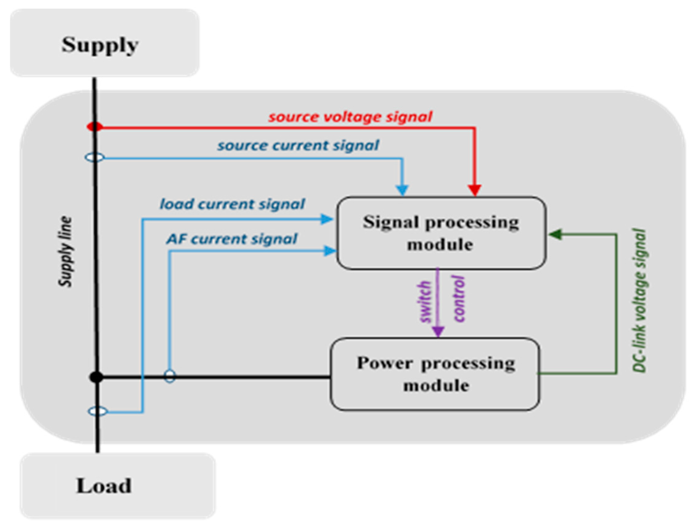
2. Method for Obtaining the Reference Signal

The method for obtaining the ShAPF reference signal considered in this article affects the operating frequency of the filter switches. Therefore, the features of this method are discussed first.
The general structure of the energy transmission system consists of four modules, namely the source, supply line, active filter, and load, as shown in Figure 1.
Shown in Figure 1, the power processing module comprises the smoothing inductor LAF, switches PA, PB, NA and NB in the full-bridge configuration, and DC-link capacitor C, as is shown in Figure 2. Description of this layout is provided in Section 3. The factor б shows the existing stand of the active filter inverter switches or the instantaneous polarity of the DC-link capacitor voltage with respect to the supply line; it is equal to +1 when the NA-PB switch pair is in the ON state and to –1 when the NB-PA pair is in the ON state.
The method applied for obtaining the reference signal is an indirect one that is based on tracking and processing of the DC-link capacitor voltage. Changes in this voltage can be used to calculate a signal that is related to the load active power [35]. This signal is modeled on the relationship (1) that is an element of the Fryze–Buchholz–Depenbrock (FBD) theory [36]:
g D = v S i L v S 2
where gD is load equivalent conductance signal, vs is instantaneous source voltage, and iL is the instantaneous load current.
The unit of the signal (1) is Siemens. Therefore, knowing the signal (1), the waveform called the Depenbrock load power current is calculated according to (2):
i p = g D v S
The expression in the numerator in Equation (1) can be processed in order to determine strictly the active power of the load. In this situation, the current (2) can be used as the reference for the supply source current at the given active power of the load. This current reference can be considered purely active.
Since the source current is controlled via the active filter action, there is inertia in response to source current/power on changes in load current/power. Because of this, a dynamic imbalance occurs between the load and the source powers. This power unevenness is balanced with the use of energy stored in the reactance elements of the active filter, namely in the DC-link capacitor C and the inductor LAF, Figure 2.
The fundamental equation describing this energy balancing, i.e., energy relations in the load active filter supply source circuit, can be written as follows:
( P L + P A F ) t = ( W A F i n i w A F ( t ) ) + 0 t v L i L d τ
where PL is the load active power; PAF is the power dissipated in the active filter circuitry; WAFini is the sum of energy accumulated in the DC-link capacitor C (stored during active filter initialization process) and some amount of energy stored in the smoothing reactor LAF; wAF(t) is the total amount of energy stored in C and LAF elements at any instant t; and vL and iL are the load voltage and current.
Equation (3) states that changes in powers PL and PAF cause transients during which these powers are balanced by two streams of power simultaneously: a stream supplied by the active filter and a stream supplied by the source. Controlling the active filter can be performed in such a way that balancing of each change in load power is carried out in an inertial manner, entirely during one period T and using only the energy stored in the reactance elements of the active filter [35]. This approach enables the use of DC-link capacitor C and the smoothing reactor LAF as sensors, giving information needed for the calculation of load active power magnitude. Thus, taking into account the energy balance (3), Equation (1) can be transformed into the form (4):
G T m = K V ( V C i n i 2 v C 2 ( T m 1 ) ) + K I ( I A F i n i 2 i A F 2 ( T m 1 ) )
where
K V = C 2 T V S 2
K I = L A F 2 T V S 2
where GTm is the load and active filter-equivalent conductance for the ongoing period Tm of the source voltage cycle; VCini is the initial voltage of the DC-link capacitor C; vC(Tm−1) is the voltage of the DC-link capacitor C at the end of period Tm−1; and IAFini and iAF(t) are the active filter currents at the moment when turning the load on, and at a given instant t, respectively; C is the capacity of the active filter’s DC-link capacitor; LAF is the inductance of active filter’s AC-side smoothing inductor; and VS is source voltage rms.
The constants KV and KI can be considered as certain parameters of the source–load–active filter system. They give proportions to energy-to-conductance relations for the DC-link capacitor voltage and active filter current, respectively. They can be used as gain coefficients for P-type regulators used in the active filter control module (the signal processing module shown in Figure 1).
Finally, the reference for the source current is as follows:
i S , T m = G T m v L
where m is the index of the ongoing T period.
Since load active power can vary, the equivalent conductance signal GTm is a step-function in time. The signal GTm is calculated mainly on the basis of changes in the voltage of the DC-link capacitor C and is marginally influenced by changes in the active filter current [35].

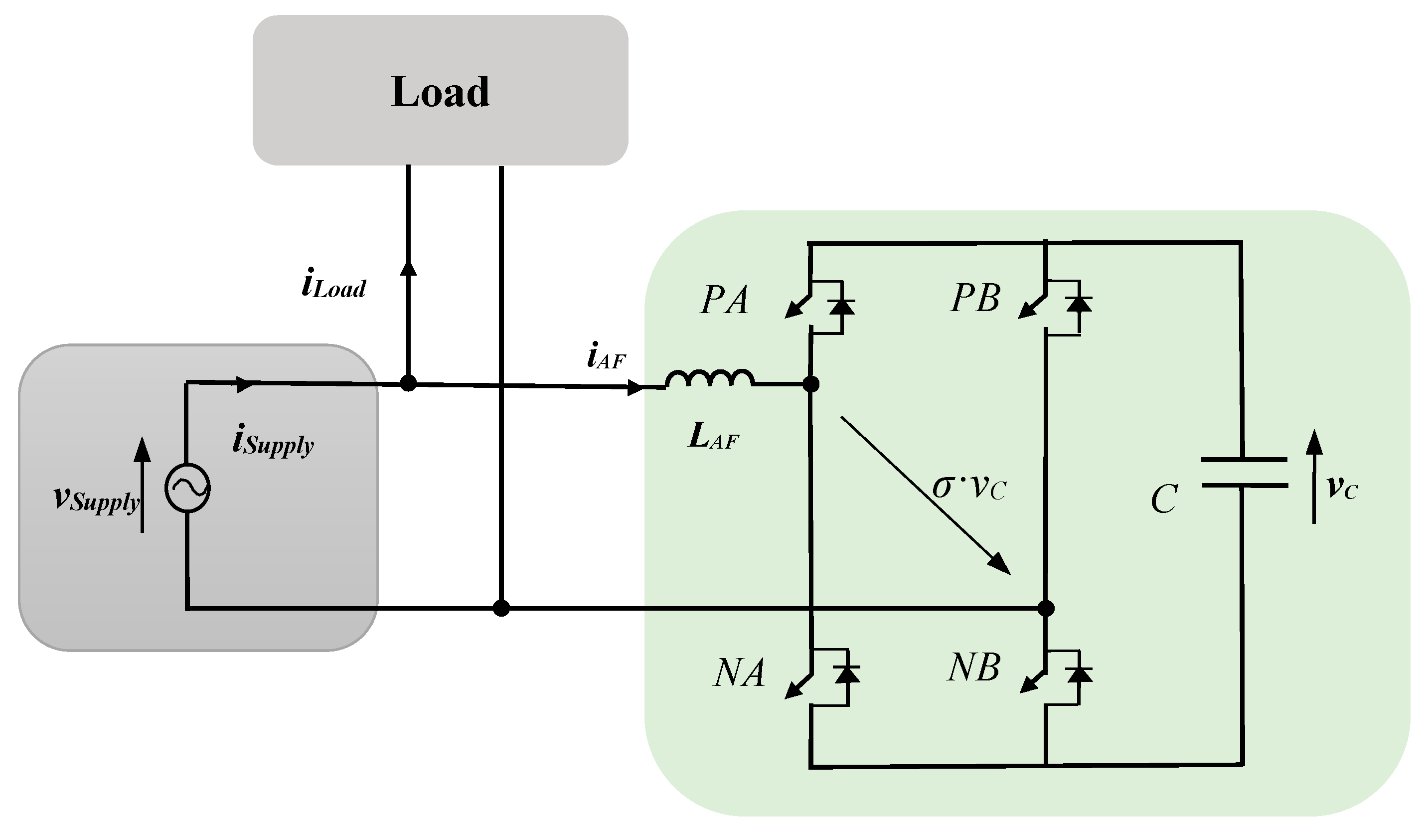
3. The Model of the Source–Load–Active Filter System

The source–load–active filter system considered has been extensively analyzed by means of computer simulation. The IsSpice software (Intusoft, San Pedro, CA, USA) has been used.
The supply source generates sinusoidal voltage of rms 230 V at 50 Hz frequency. Internal resistance and inductance of the supply voltage source is 2 mΩ and 100 μH, respectively.
The load consists of three branches in parallel. The first branch consists of a thyristor power controller that is composed of a 10 Ω resistor in series with two thyristors in antiparallel connection. Both thyristors are fired symmetrically with phase angle π/2. This branch brings in two abrupt load current changes in every period T, which are a challenge for the active filter. The second branch consists of a diode and a 20 Ω resistor. This branch brings in a DC component to the load current. The third branch is composed of an Ω resistor and a 63.7 mH inductor, bringing in an inductive phase displacement to the load current.
Concerning the active filter, energy changes in the DC-link capacitor are essential for obtaining the current reference signal. The capacity of the DC-link capacitor C is rated with respect to the maximal magnitude PLmax of the load active power and the DC-link maximal-to-minimal voltage ratio. Thus, the needed capacity can be estimated as C = 2PLmax/(VCini2 − vcT12). For the analysis, an initial voltage VCini of 500 V and a C capacity of 4 mF are used. A hysteresis regulator operating with a ∆I loop equal to 1 A is used to shape the reference current. The inductance LAF for the converter’s series inductor is set to 5 mH in order to limit the maximum switching frequency to about 25 kHz. Switching elements of the converter are modeled to work as simplified IGBT transistors.
The load current iLoad and supply source current iSupply are shown in Figure 3, and the DC-link capacitor voltage vC and conductance signal GTm (4) are shown in Figure 4. The active filter already works when the load is turned on at time t1 = 20 ms. During the first period T1 of load activity, i.e., for time period 20–40 ms, the load is powered only with the use of energy stored in the active filter. Therefore, there is no supply current shown in Figure 3 for this period, and, simultaneously, a “static” DC-link capacitor voltage drop can be seen in Figure 4 for the same time period. Just after period T1 is completed, the conductance signal GT2 rises to a magnitude that is proportional to the load active power. Thus, the amplitude for the source current is already determined (7). Therefore, starting from time t2 = 40 ms, the source takes over the entire active power delivered to the load.
The conductance signal GT1 lags slightly behind at moment t2 = 40 ms, Figure 4. This is due to the filtering of the source voltage vSupply, which somewhat delays this waveform. Beginning from time t2 = 40 ms, two components in the DC-link capacitor voltage can be distinguished. The former, which can be called static, results from the indirect method of measuring the active power of the load. Equation (4) shows that the amount of active power drawn from the source is calculated by processing the signal of the voltage drop of the DC-link capacitor C. Therefore, the DC-link voltage is not stabilized. As a result, the following dependence appears: the higher the active power of the load, the lower the rate of change in the filter current or filter dynamics. The latter voltage component, the one that is oscillating, results from the compensation for the nonactive component of the load current, see (9) in Section 4.1.

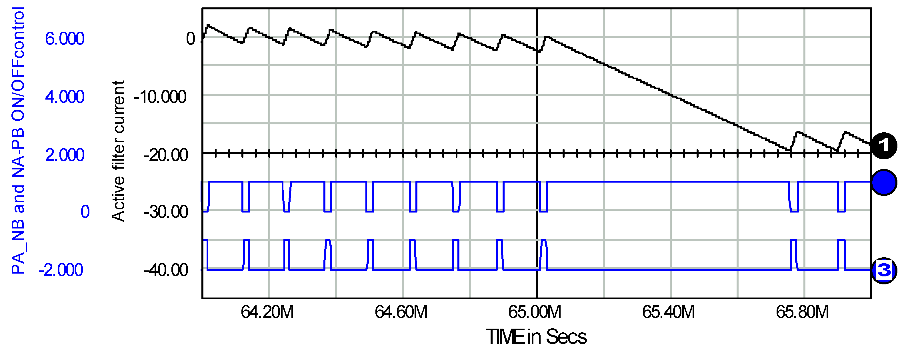
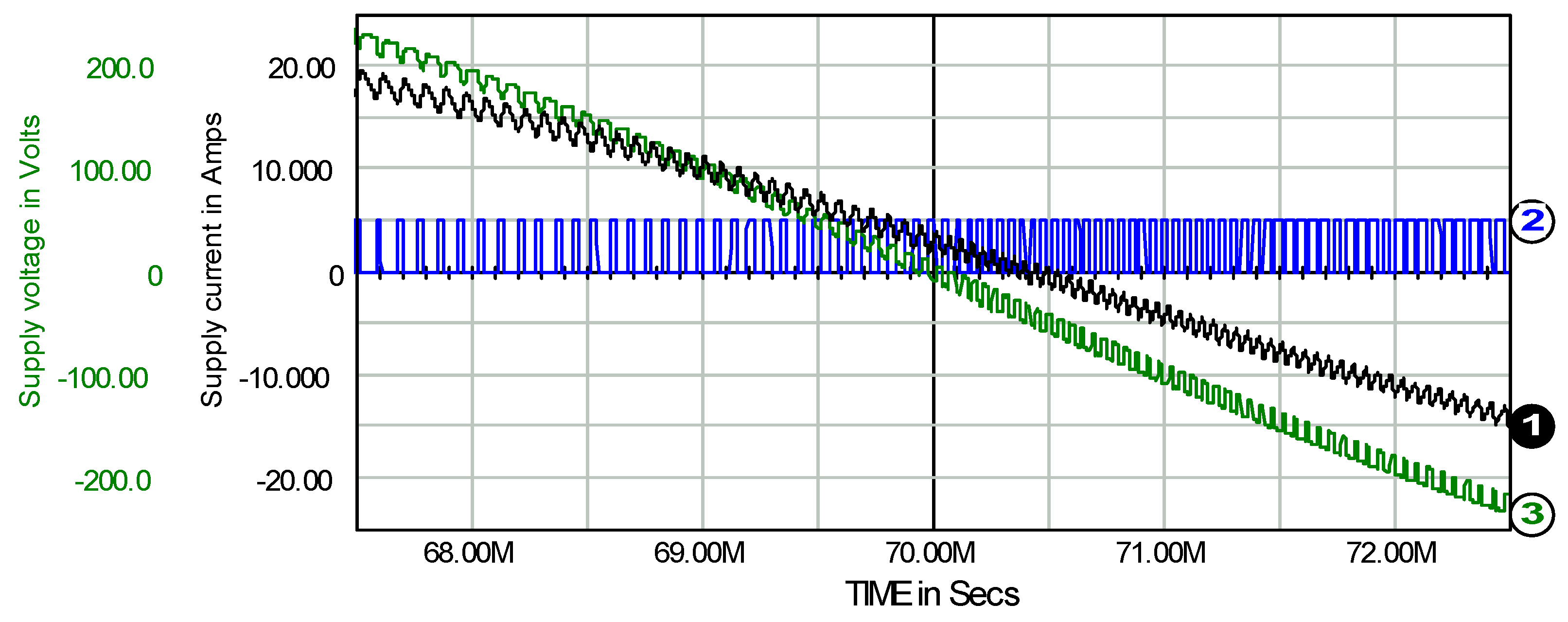
4. Continuous and Discontinuous Use of the DC-Link Capacitor Energy

The active filter should have the ability to keep up with rapid changes in load current. To meet this requirement the voltage-source inverter with a hysteresis current-control technique seems to be a good solution. In particular, the conventional hysteresis control technique has very fast response speed, without delay by analog-to-digital conversions or computations. This technique, if used in a closed-loop system, enables direct regulation of the line current, which also helps to accurately achieve the control goal.
The active filter dynamics, and consequently also the frequency of its switches action, depends on the instantaneous voltage on the LAF inductor, i.e., on the difference between the instantaneous DC-link capacitor voltage and the instantaneous AC-side voltage, Figure 2. The greater the difference, the greater the rate of change in the filter current and the shorter the time to reduce the current error, i.e., to reduce the difference between the actual source current and the reference current (7). From this point of view, the instantaneous voltage of the DC-link capacitor must always be much greater than the instantaneous voltage on the AC side, i.e., vC >> vS. However, the price behind the higher dynamics is the higher frequency of its switches action and, therefore, the higher power loss in the active filter switches. As shown in Section 4.1, however, in some situations it is possible to waive the requirement vC >> vS. Despite this, the source current waveform is still kept within the required range defined by the hysteresis bandwidth. The benefit achieved is the reduction in power losses in the active filter switches.

4.1. Shaping the Source Current with Continuous Use of DC-Link Capacitor Energy

Equations (8) and (9) describe current and voltage relations in the system considered, as shown in Figure 2.
d i S d t = v S + σ v C L A F + d i L d t
d v C d t = σ ( i L i S ) C
where iS is the source current (iSupply), vS is the source voltage (vSupply), σ is the switching factor, vC is the DC-link capacitor voltage, LAF is the inductance of the active filter smoothing inductor, and iL is the load current (iLoad)
The factor σ is equal to +1 when the pair NA-PB of filter switches is in state ON (the pair PA-NB is then OFF), and is equal to −1 when the pair PA-NB is ON (NA-PB is OFF). The current of the active filter is shaped as follows: The source current is compared with a tolerance band ΔI around the reference (7). The pair PA-NB is turned ON (σ is equal to −1) if the source current rises above the upper tolerance limit, and the pair NA-PB is turned ON (σ is equal to +1) if the source current falls below the lower tolerance limit.
While active, the active filter maintains the supply current to be active according to (7) regardless the load current waveform. Four combinations for the polarity of the source voltage vS and the capacitor voltage vC can be distinguished:
(a)
vS ≥ 0 and PA-NB pair is in state ON;
(b)
vS ≥ 0 and NA-PB pair is in state ON;
(c)
vS < 0 and PA-NB pair is in state ON;
(d)
vS < 0 and NA-PB pair is in state ON.
Analysis of these four combinations is provided below.
-
Combination (a): vS ≥ 0 and PA-NB pair is in state ON
Since σ is equal to −1, Equation (8) takes the form:
d i S d t = v S v C L A F + d i L d t
Taking into account that the DC-link capacitor voltage vC is positive and must be considerably greater than the source voltage vS, the following inequality is satisfied:
v S v C L A F < 0
Inequality (11) can combine with three cases of load current rate of change (a1)–(a3):
( a 1 ) | v S v C L A F | > | d i L d t |
( a 2 ) | v S v C L A F | < | d i L d t |
( a 3 ) | v S v C L A F | = | d i L d t |
ad. (a1) Source current is reduced and the derivative diS/dt is negative.
ad. (a2) The case considered in this point occurs at the moment t3 = 65 ms, Figure 5. This is the situation when the slope of the load current exceeds the achievable rate of change in the active filter current. This results in a temporary inability for the active filter to shape the grid current according to a sinusoidal reference, which is defined by relation (7). This phenomenon manifests itself as a spike in the source current waveform and, at the same time, as a filter current linear drop, Figure 5 (waveforms in Figure 5 are consistent with those shown in Figure 3), and waveform 1 in Figure 6. In this situation, the hysteresis controller operates to decrease the source current, which is realized as a negative derivative diS/dt demand. However, this demand cannot be met if the derivative diL/dt is positive and when the load current rate of change is greater than the filter current dynamics. Despite the forced decrease, the source current increases, causing growth in the error of the source current control. The filter counteracts this error by keeping this pair of switches ON, which forces the source current to fall, i.e., the pair PA-NB. After the load current reaches the magnitude resulting from the instantaneous value of the load power, the filter reduces the source current until the current error reaches the tolerance limit of the opposite sign. The conductive pair of switches is then changed.
Figure 6 shows the active filter current and the ON/OFF control signals for the PA-NB and NA-PB pairs of switches for the case discussed in this point.
ad. (a3) The operation of the system in the case of comparable rate of change in both the active filter current and the load current results from the analysis shown in points (a1) and (a2). If the derivatives of the filter and load currents are of the same sign, i.e., the load current decreases, the duty cycle of the PA-NB pair is shortened. On the other hand, if these derivatives are of the opposite sign, the source current is kept constant, and the change in the conductive pair of switches occurs due to an increase in the current error caused by the run of the source voltage.
-
Combination (b): vS ≥ 0 and NA-PB pair is in state ON
The factor σ is equal to +1; therefore Equation (8) takes the form:
d i S d t = v S + v C L A F + d i L d t
It can be seen that:
v S + v C L A F > 0
which means that the control system forces a positive derivative of the source current, i.e., an increase in its magnitude. Taking into account possible combinations of sign and magnitude of the component diL/dt, the reasoning analogous to that performed in points (a1)–(a3) above can be carried out.
-
Combination (c): vS < 0 and PA-NB pair is in state ON
Since σ is equal to −1, Equation (8) takes the form:
d i S d t = v S v C L A F + d i L d t
The control circuit of the active filter steers the inverter to increase the source current magnitude according to the running source voltage polarity. The influence of the component diL/dt on this process is described in the above analysis.
-
Combination (d): vS < 0 and NA-PB pair is in state ON
The factor σ equals +1, therefore Equation (8) takes the form:
d i S d t = v S + v C L A F + d i L d t
Taking into account that vCmin > √2VSupply, it can be concluded that the control circuit tends to reduce the absolute value of the source current. Further analysis of this case is similar to that given above.
Summarizing items (a)–(d): When the instantaneous source voltage is positive (or zero), then—on the basis of points (a) and (b)—it can be concluded that the activation of a pair of PA-NB switches results in a reduction in the filter current value, and, with a negligible rate of change in the load current component diL/dt, also in a reduction in the source current. On the other hand, turning ON the NA-PB pair causes an increase in the filter current and, with a negligible diL/dt component, also an increase in the source current. In turn, when the source voltage is negative, then—items (c) and (d)—turning on the PA-NB switches causes an increase (in absolute value) in the filter current, and, with a negligible rate of change in the load current, also the source current. On the other hand, turning on the NA-PB switches causes a decrease (in absolute value) in the filter current, and, with a negligible rate of change in the load current, also the source current. Thus, an exchange of current increasing/diminishing functions in the pairs of PA-NB and NA-PB switches is observed, depending on the sign of the source voltage.

4.2. Shaping the Source Current with Discontinuous Use of DC-Link Capacitor Energy

Assuming that the rate of change in active filter current is much greater than the load current rate of change,
| v S + σ v C L A F | > > | d i L d t |
then Equation (8) takes the form:
d i S d t = v S + σ v C L A F
Turning on a given pair of switches causes the filter current to change by 2∆I. Hence, the ON time for the given pair of switches is:
t O N = 2 Δ I L A F | v S + σ v C |
To find short operating cycles for the hysteresis controller (or high switching frequency), the following three cases should be considered:
(1) vS = vSmax at σ = +1 and then at σ = −1;
(2) vS = −vSmax at σ = +1 and then at σ = −1;
(3) vS = 0 at σ = +1 and then at σ = −1.
ad. (1) The periods of being ON for both pairs of switches are:
t O N , N A P B = 2 Δ I L A F v S max + v C
t O N , P A N B = 2 Δ I L A F | v S max v C |
It can be stated that:
  • tON,NA-PB < tON,PA-NB;
  • The sign of the total voltage in the denominator of expression (22) is consistent with the sign of the source voltage and, on the contrary, in the denominator of expression (23) is the opposite.
ad. (2) The ON periods for both pairs of switches are:
t O N , N A P B = 2 Δ I L A F v S max + v C
t O N , P A N B = 2 Δ I L A F | v S max v C |
In this point:
  • tON,NA-PB < tON,PA-NB;
  • The sign of the total voltage in the denominator of expression (24) is opposite the sign of the source voltage, but consistent in the denominator of expression (25).
ad. (3) In this case:
t O N , N A P B = 2 Δ I L A F v C
t O N , P A N B = 2 Δ I L A F | v C |
It should be noted that:
  • tON,NA-PB = tON,PA-NB;
  • The sum of both periods tON,NA-PB + tON,PA-NB is the smallest, i.e., the switching frequency is the highest in this case;
  • The case discussed here concerns a supply voltage that is close to zero
This discussion shows that in some cases, namely those for which in the denominator of expression (21) the sign of the total voltage is consistent with the sign of the source voltage, it is possible to extend the switching ON time for the appropriate pair of switches. This possibility can be realized by temporarily blocking the influence of the DC-link capacitor voltage on the active filter current. As a result, only the source voltage appears on the LAF inductor. For this purpose, the NA-NB pair (or the PA-PB pair, what leads to the same effects) should be activated at appropriate time intervals. In these cases, the factor σ is equal to 0. In relation to point ad. (3), it should be expected that for the use of the additional (third) control state, σ = 0 gives the greatest effect when the supply voltage is close to zero.

5. Logic System for Three-State Control Technique σ ϵ (+1, −1, 0)

The implementation of the three-state control technique can be realized using voltage sensors and logic gates. The logic signals CW, CS, and CH, which are used to control the action of inverter switches PA, PB, NA, and NB, are as follows:
P A = C W C S ¯ ¯ C H ¯ P B = C W C S ¯ C H
N A = C W C S ¯ + C H N B = C W C S + C H ¯
where CW eq. Hi activates three-state control when the supply voltage is within the declared range, CS eq. Hi indicates a positive half-wave of the supply voltage, and CH is the switching ON/OFF control signal at the output of the hysteresis controller
The CW signal is generated by a window voltage detector (window comparator) that tracks the supply voltage. The high level of the CW signal enables the three-state control, i.e., allows the sum of the DC-link capacitor vC and supply voltages vS to be replaced by only the supply voltage vS. Disconnection of the DC-link capacitor voltage, forced by applying the control state σ = 0, causes simultaneous conduction of the NA-NB switches. For the positive half-wave of the supply voltage waveform, the switch PB is continuously OFF, the NB switch is continuously ON, and the switches PA and NA are controlled ON/OFF alternately. Similarly, for the negative half-wave of the supply voltage, the switch PA is continuously OFF, the NA switch is continuously ON, and the switches PB and NB are controlled ON/OFF alternately.
Since the highest switching frequency is expected to occur in the low to medium range of instantaneous supply voltage, the three-state control of the inverter switches can or should be activated for this range, especially. The results of using the three-state control are presented in Figure 7, Figure 8 and Figure 9.
In Figure 7, the active filter works without activating the three-state control, i.e., for σ equal to +1 or −1 only ϵ (+1, −1). The number of pulses generated by the hysteresis controller during the time period 69.4–71.4 ms, i.e., when the instantaneous supply voltage is in the low-to-medium range ±100 V, is 28 (waveform 2).
In Figure 8, the active filter already works in the three-state control regime, which is activated for the same supply voltage range, about ±100 V. The number of pulses generated by the hysteresis controller during the same time period, 69.4–71.4 ms, then waveform 2 is 6 for the three-state control. This is almost five times less compared with the two-state control.
Figure 9 shows a full T period comparison of the two-state control, waveform 1, versus the three-state control, waveform 2. For waveform 1, a relatively high and regular operating frequency of the hysteresis controller can be observed (with the exception of moments of rapid load power changes: approximately at instants 65 and 75 ms). Contrarily, for waveform 2, the areas with significantly smaller switching frequencies can be seen. This always occurs when the supply current is close to zero.
Table 1 collects comparative data for the high-frequency components of the waveforms presented in Figure 9. They show their characteristics in the time domain. A significant reduction in the switching frequency was observed for the three-state control. As expected, the greatest reduction in switching frequency occurs during those time periods when the source voltage is close to zero.
Table 2 contains the same parameters as shown in Table 1, but this time obtained for the time period 0–20 ms, that is, with the active filter already in operation, but before the load is turned on (see Figure 3). Since the DC-link capacitor voltage is at its maximum during this period, see (3) and Figure 4, the maximum switching frequency then occurs, especially when source voltage is close to zero, see (26) and (27). It can be seen that for these conditions the frequency reduction effect is considerable as well.
It can be generally stated that if the three-state control is used, the switching power loss in the inverter switches can be significantly reduced.

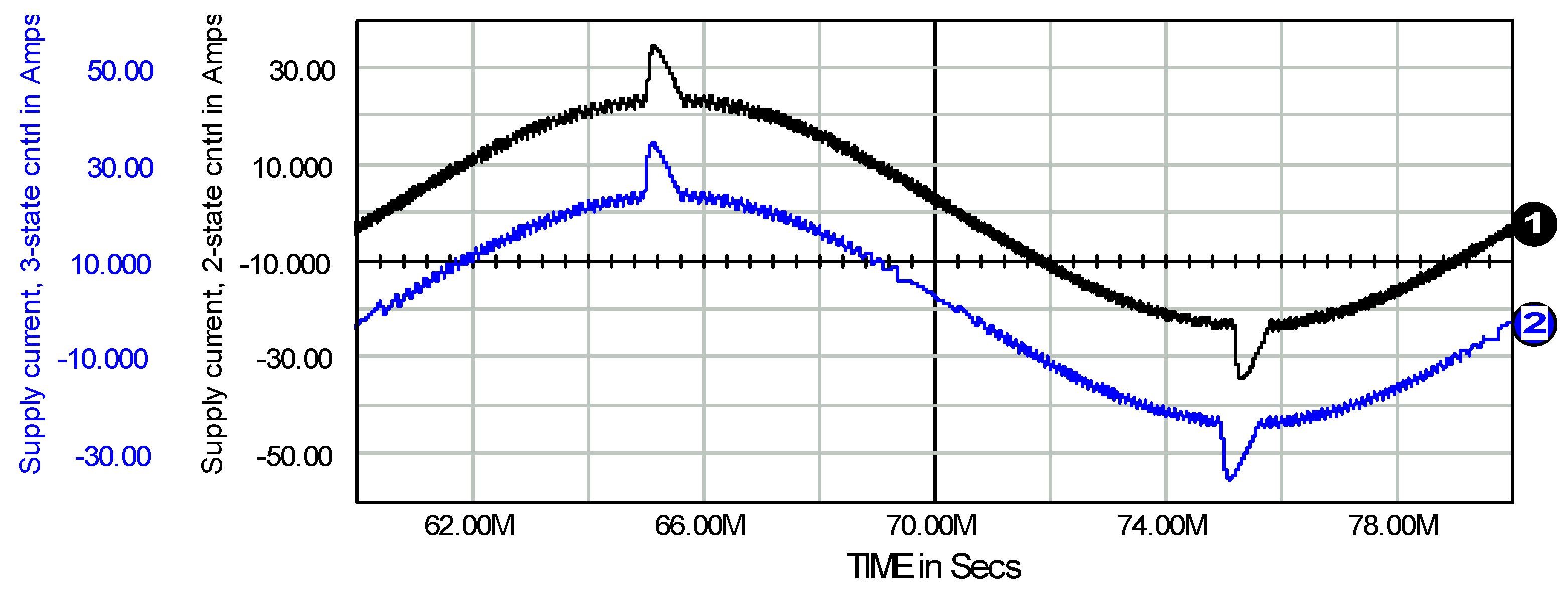
6. Two- or Three-State Control Technique vs. Conductance Signal Accuracy

6.1. Conductance Signal Accuracy

Since the voltage of the DC-link capacitor is tracked to obtain the conductance signal (4), it should be investigated whether the use of the three-state control can significantly interfere with the accuracy of the conductance signal obtained. All voltage and current signals analyzed in this section are the same as those considered previously.
A comparison of the DC-link capacitor current for the three-state vs. the two-state control technique is shown in Figure 10. For the time period shown, the number of current pulses decreases by 45% and the rms current decreases by 26% for the three-state control.
As a result, there is a change in the energy flow between the DC-link capacitor and the source. Therefore, there can be some risk that the waveform of the DC-link capacitor voltage and, consequently, the conductance signal (4) can be somewhat disturbed. However, from Figure 10, results that for the three-state control the current pulses are unipolar in subsequent time intervals, waveform 2, and that there is a symmetrical compensation in the electric charge flow in relation to the bipolar pulses for the two-state control, shown in waveform 1. As a result, in the steady state there is still zero mean energy flow during the period T, so there is no distortion of the information about the actual active power of the load.
The phenomenon of zero mean energy flow through the DC-link capacitor described above may not occur in the case of a time-variable load if the power change appears within the period T. In such a situation, the total change in the charge of the DC-link capacitor within the period T is nonzero, so a certain imbalance in the active power of the source in relation to the current active power of the load arises in this T period. However, it follows from (4) that such an imbalance tends to be corrected in subsequent periods T. The imbalance can be also “covered” by changes in active power of the time-variable load or in supply voltage characteristics.
Summarizing, the use of the three-state control can cause slight oscillations around the exact waveform in the conductance signal G, but cannot significantly decrease the active filter’s compensating properties.
To illustrate this statement, the load current, the supply current, and the conductance signal for a very changeable load are shown in Figure 11. The load is turned on at t = 20 ms when the active filter is already working. The load starts and ends with the same current waveform associated with the same active power: 20–60 ms and 140–200 ms. These two periods are separated by a time interval of rapid and irregular power changes: 60–140 ms. In all of these time intervals, the active filter acts correctly. The conductance signal follows the changes in load active power properly and stabilizes its magnitude during periods of constant active power.

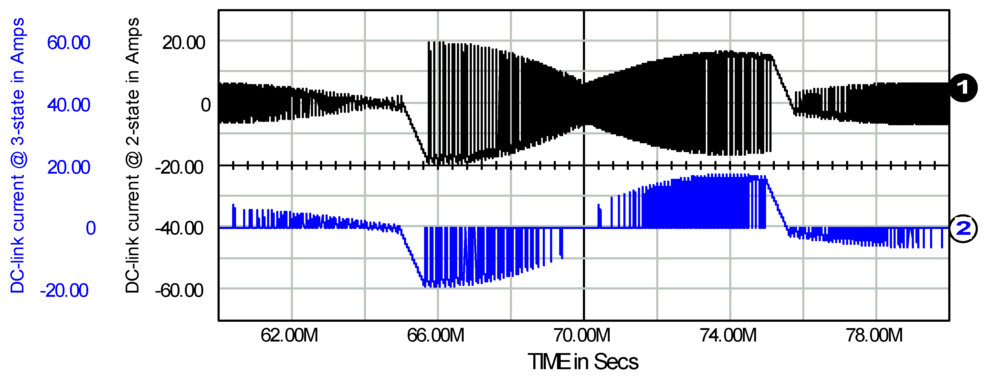
6.2. DC-Link Capacitor Lifetime

There is a common engineering regularity that is important from this article’s point of view: “electrolytic capacitors and power modules are the two most fragile components which are also prone to wear-out failure”, as stated in [37]. Other important principles that improve the DC-link capacitor lifetime can be achieved by reducing the current flowing through it, and, in particular, by lowering the capacitor current ripple, which can be found in, e.g., [38,39,40,41]. The data collected in Table 1 and Table 2 and the analysis of the waveforms shown in Figure 10 indicate that using the three-state control technique provides such advantages.

7. Conclusions

The shunt active power filter can operate on the basis of various power theories and current control techniques. In particular, the efficiency of the active filter, which operates on the basis of the conductance signal as a tool for obtaining the reference signal, can be improved if the conventional hysteresis control technique is modified in some way. It was shown in the paper that the application of the described three-state control technique, which relies on discontinuous use of DC-link capacitor energy, can lower the energy loss in the filter maintaining the accuracy of the ShAPF control. The use of the three-state control gives significant utility benefits resulting from the reduction in the pulse frequency of the ShAPF switching elements and the diminishing of the rms value of the DC-link capacitor current:
Energy loss in the switching elements and the DC-link capacitor is reduced;
Operating temperature of switches and other elements of the active filter can be diminished;
Current ripples in the DC-link capacitor decrease;
DC-link capacitor lifetime increases;
High-frequency components in supply voltage/current waveforms decrease.
The considerations presented are of a general nature, therefore no specific amount of energy saved in the switches or extension in the life of the DC-link capacitor are shown. There are many possibilities to use the various elements, made by using different technologies and by different manufacturers. However, the advantages shown can be obtained for any ShAPF implementation technology.

Funding

This research received no external funding.

Data Availability Statement

No new data other than those included in the article were created.

Conflicts of Interest

Author declares no conflict of interest.

References

  1. Bollen, M. What is power quality? Electr. Power Syst. Res. 2003, 66, 5–14. [Google Scholar] [CrossRef]
  2. Sharmaa, A.; Rajpurohita, B.S.; Singh, S.N. A review on economics of power quality: Impact, assessment and mitigation, Renewable and Sustainable. Energy Rev. 2018, 88, 363–372. [Google Scholar]
  3. Caramia, P.; Carpinelli, G.; Verde, P. Power Quality Indices in Liberalized Markets; John Wiley & Sons: Hoboken, NJ, USA, 2009. [Google Scholar]
  4. Zhang, X.-P.; Yan, Z. Energy Quality: A Definition. IEEE Open Access J. Power Energy 2020, 7, 430–440. [Google Scholar] [CrossRef]
  5. Benysek, G.; Kazmierkowski, M.P.; Popczyk, J.; Strzelecki, R. Power electronic systems as a crucial part of Smart Grid infrastructure—A survey. Bull. Pol. Acad. Sci. Tech. Sci. 2011, 59, 455–473. [Google Scholar] [CrossRef]
  6. Dixon, J.W.; Ooi, B.T. Indirect current control of a unity power factor sinusoidal current boost type three-phase rectifier. IEEE Trans. Ind. Electr. 1988, 35, 508–515. [Google Scholar] [CrossRef]
  7. Garcia, O.; Cobos, J.; Prieto, R.; Alou, P.; Uceda, J. Single Phase Power Factor Correction: A Survey. IEEE Trans. Power Electron. 2003, 18, 749–755. [Google Scholar] [CrossRef]
  8. Kolar, J.; Friedli, T. The Essence of Three-Phase PFC Rectifier Systems—Part I. IEEE Trans. Power Electron. 2013, 28, 176–198. [Google Scholar] [CrossRef]
  9. Friedli, T.; Hartmann, M.; Kolar, J. The Essence of Three-Phase PFC Rectifier Systems—Part II. IEEE Trans. Power Electron. 2013, 29, 543–560. [Google Scholar] [CrossRef]
  10. Nguyen, H.-N.; Nguyen, M.-K.; Duong, T.-D.; Tran, T.-T.; Young-Cheol Lim, Y.-C.; Choi, J.-H. A Study on Input Power Factor Compensation Capability of Matrix Converters. Electronics 2020, 9, 82. [Google Scholar] [CrossRef]
  11. Sannio, A.; Svensson, J.; Larsson, T. Power-electronic solutions to power quality problems. Electr. Power Syst. Res. 2003, 66, 71–82. [Google Scholar] [CrossRef]
  12. Awad, H.; Bollen, M. Power electronics for power quality improvements. In Proceedings of the IEEE International Symposium on Industrial Electronics, Rio de Janeiro, Brazil, 9–11 June 2003. [Google Scholar]
  13. Alfonso, J.L.; Tanta, M.; Pinto, J.G.; Monteiro, L.F.; Machado, L.; Sousa, T.J.; Monteiro, V. A Review on Power Electronics Technologies for Power Quality Improvement. Energies 2021, 14, 8585. [Google Scholar] [CrossRef]
  14. Szulborski, M.; Kolimas, Ł.; Łapczyński, S.; Szczęśniak, P. Single phase UPS systems loaded with nonlinear circuits: Analysis of topology in the context of electric power quality. Arch. Electr. Eng. 2019, 68, 787–802. [Google Scholar] [CrossRef]
  15. Green, T.C.; Marks, J.H. Control techniques for active power filters. IEEE Proc. Power Appl. 2005, 152, 369–381. [Google Scholar] [CrossRef]
  16. Asiminoaei, L.; Blaabjerg, F.; Hansen, S. Detection is key. Harmonic detection methods for active power filter applications. IEEE Ind. Appl. Mag. 2007, 13, 22–33. [Google Scholar] [CrossRef]
  17. Bhattacharya, A.; Chakraborty, C.; Bhattacharya, S. Shunt compensation. Reviewing traditional methods of reference current generation. IEEE Ind. Electron. Mag. 2009, 3, 38–49. [Google Scholar] [CrossRef]
  18. Revuelta, P.S.; Litran, S.P.; Thomas, J.P. Active Power Line Conditioners Design, Simulation and Implementation for Improving Power Quality; Academic Press: Cambridge, MA, USA; Elsevier: Amsterdam, The Netherlands, 2016. [Google Scholar]
  19. Sozański, K. Digital Signal Processing in Power Electronics Control Circuits; Springer: Berlin/Heidelberg, Germany, 2017. [Google Scholar]
  20. Benysek, G.; Pasko, M.; Maciążek, M.; Sozański, K.; Jarnut, M.; Kaniewski, J. Power Theories for Improved Power Quality; Springer: Berlin/Heidelberg, Germany, 2012. [Google Scholar]
  21. Xia, Y.; Roy, J.; Ayyanar, R. Optimal Variable Switching Frequency Scheme to Reduce Loss of Single-Phase Grid-Connected Inverter With Unipolar and Bipolar PWM. IEEE J. Emerg. Sel. Top. Power Electron. 2019, 9, 1013–1026. [Google Scholar] [CrossRef]
  22. Zygmanowski, M.; Grzesik, B.; Fulczyk, M.; Nalepa, R. Analytical and Numerical Power Loss Analysis in Modular Multilevel Converter. In Proceedings of the IECON 2013—39th Annual Conference of the IEEE Industrial Electronics Society, Vienna, Austria, 10–13 November 2013. [Google Scholar]
  23. Zygmanowski, M. Detailed Power Loss Analysis of T-Type Neutral Point Clamped Converter for Reactive Power Compensation. Electronics 2022, 11, 2129. [Google Scholar] [CrossRef]
  24. Oeder, C.; Barwig, M.; Duerbaum, T. Estimation of Switching Losses in Resonant Converters Based on Datasheet Information. In Proceedings of the 2016 18th European Conference on Power Electronics and Applications (EPE’16 ECCE Europe), Karlsruhe, Germany, 5–9 September 2016. [Google Scholar]
  25. Asiminoaei, L.; Rodriguez, P.; Blaabjerg, F.; Malinowski, M. Reduction of Switching Losses in Active Power Filters With a New Generalized Discontinuous-PWM Strategy. IEEE Trans. Ind. Electron. 2008, 55, 467–471. [Google Scholar] [CrossRef]
  26. Gurpinar, E.; Castellazzi, A. Single-Phase T-Type Inverter Performance Benchmark Using Si IGBTs, SiC MOSFETs, and GaN HEMTs. IEEE Trans. Power Electron. 2016, 31, 7148–7160. [Google Scholar] [CrossRef]
  27. Szular, Z.; Rozegnał, B.; Mazgaj, W. A New Soft-Switching Solution in Three-Level Neutral-Point-Clamped Voltage Source Inverters. Energies 2021, 14, 2247. [Google Scholar] [CrossRef]
  28. Sojka, P.; Pipiska, M.; Frivaldski, M. GaN power transistor switching performance in hard-switching and soft-switching modes. In Proceedings of the 2019 20th International Scientific Conference on Electric Power Engineering (EPE), Kouty nad Desnou, Czech Republic, 15–17 May 2019. [Google Scholar]
  29. Oswald, N.; Anthony, P.; McNeill, N.; Stark, B.H. An Experimental Investigation of the Tradeoff between Switching Losses and EMI Generation With Hard-Switched All-Si, Si-SiC, and All-SiC Device Combinations. IEEE Trans. Power Electron. 2014, 29, 2393–2407. [Google Scholar] [CrossRef]
  30. Bazzi, A.M.; Krein, P.T.; Kimball, J.W.; Kepley, K. IGBT and Diode Loss Estimation Under Hysteresis Switching. IEEE Trans. Power Electron. 2012, 27, 1044–1048. [Google Scholar] [CrossRef]
  31. Buso, S.; Malesani, L.; Mattavelli, P. Comparision of Current Control Techniques for Active Filter Applications. IEEE Trans. Ind. Electron. 1998, 45, 722–729. [Google Scholar] [CrossRef]
  32. Kale, M.; Ozdemir, E. An adaptive hysteresis band current controller for shunt active power filter. Electr. Power Syst. Res. 2005, 73, 113–119. [Google Scholar] [CrossRef]
  33. Awasthi, A.; Patel, D. Implementation of Adaptive Hysteresis Current Control Technique for Shunt Active Power Conditioner and Its Comparison with Conventional Hysteresis Current Control Technique. In Proceedings of the 2017 IEEE International Conference on Signal Processing, Informatics, Communication and Energy Systems (SPICES), Kollam, India, 8–10 August 2017. [Google Scholar]
  34. Kaźmierkowski, M.; Malesani, L. Current Control Techniques for Three-Phase Voltage-Source PWM Converters: A Survey. IEEE Trans. Ind. Electron. 1998, 45, 691–703. [Google Scholar] [CrossRef]
  35. Szromba, A. Is It Possible to Obtain Benefits by Reducing the Contribution of the Digital Signal Processing Techniques to the Control of the Active Power Filter? Energies 2021, 14, 6031. [Google Scholar] [CrossRef]
  36. Depenbrock, M.; Staudt, V. The FBD-method as tool for compensating non-active currents. In Proceedings of the 8th Inter-national Conference on Harmonics and Quality of Power, Athens, Greece, 14–16 October 1998; pp. 320–324. [Google Scholar]
  37. Peyghami, S.; Blaabjerg, F.; Palensky, P. Incorporating Power Electronic Converters Reliability Into Modern Power System Reliability Analysis. IEEE J. Emerg. Sel. Top. Power Electron. 2021, 9, 1668–1681. [Google Scholar] [CrossRef]
  38. Yang, S.; Xiang, D.; Bryant, A.; Mawby, P.; Ran, L.; Tavner, P. Condition Monitoring for Device Reliability in Power Electronic Converters: A Review. IEEE Trans. Power Electron. 2010, 25, 2734–2752. [Google Scholar] [CrossRef]
  39. Wang, H.; Blaabjerg, F. Reliability of Capacitors for DC-Link Applications in Power Electronic Converters—An Overview. IEEE Trans. Ind. Appl. 2014, 50, 3569–3578. [Google Scholar] [CrossRef]
  40. Kim, Y.-J.; Kim, S.-M.; Lee, K.-B. Improving DC-Link Capacitor Lifetime for Three-Level Photovoltaic Hybrid Active NPC Inverters in Full Modulation Index Range. IEEE Trans. Power Electron. 2021, 36, 5250–5261. [Google Scholar] [CrossRef]
  41. Sharma, P.K.; Vijayakumar, T. Study of Capacitor & Diode Aging effects on Output Ripple in Voltage Regulators and Prognostic Detection of Failure. Intl. J. Electron. Telecommun. 2022, 68, 281–286. [Google Scholar]
Figure 1. Source–supply line–load with the block diagram of the active filter.
Energies 16 04080 g001
Figure 2. Power processing module of the active filter: voltage-source inverter.
Energies 16 04080 g002
Figure 3. Load current iLoad and supply (source) current iSupply: waveforms 1 and 2, respectively.
Energies 16 04080 g003
Figure 4. DC-link capacitor voltage vC and conductance signal GTm: waveforms 1 and 2, respectively.
Energies 16 04080 g004
Figure 5. Supply (source) current iSupply, active filter current iAF, and current error (iS,Tm* − iSupply): waveforms 1, 2, and 3, respectively.
Energies 16 04080 g005
Figure 6. Active filter current iAF and control ON/OFF signal of switches PA-NB and NA-PB: waveforms 1, 2, and 3, respectively.
Energies 16 04080 g006
Figure 7. Two-state switches control. Supply (source) current, hysteresis controller switching ON/OFF signal, and supply voltage run: waveforms 1, 2, and 3, respectively.
Energies 16 04080 g007
Figure 8. Three-state switches control. Supply (source) current, hysteresis controller switching ON/OFF signal, supply voltage run, and three-state control enable signal: waveforms 1, 2, 3, and 4, respectively.
Energies 16 04080 g008
Figure 9. Comparison of the source current for two-state and three-state switches control technique: waveform 1 and waveform 2, respectively.
Energies 16 04080 g009
Figure 10. DC-link capacitor current for two-state and three-state control: waveform 1 and waveform 2, respectively.
Energies 16 04080 g010
Figure 11. Three-state control: load current, supply current, and conductance signal G, waveform 1, 2, and 3, respectively. Both current waveforms are shown with the same Y scale.
Energies 16 04080 g011
Table 1. Comparative data for the supply current waveforms shown in Figure 9, avg(fsw) is the average switching frequency during the time period 60–80 ms.
Control MethodNumber of Pulses in Time Period in MillisecondsFrequency
60–64 ms64–68 ms68–72 ms72–76 ms76–80 ms60–80 msavg(fsw) Hz
2-state493068476025412,700
3-state, 100 V range34293646501959750
3-state, 325 V range28262033321396950
Table 2. Comparative data for the supply current waveforms–no load power condition, avg(fsw) is average switching frequency during the time period 0–20 ms.
Control MethodNumber of Pulses in Time Period in MillisecondsFrequency
0–4 ms4–8 ms8–12 ms12–16 ms16–20 ms0–20 msavg(fsw) Hz
2-state836593658138719,350
3-state, 100 V range576653656931015,500
3-state, 325 V range39472747381989900
Disclaimer/Publisher’s Note: The statements, opinions and data contained in all publications are solely those of the individual author(s) and contributor(s) and not of MDPI and/or the editor(s). MDPI and/or the editor(s) disclaim responsibility for any injury to people or property resulting from any ideas, methods, instructions or products referred to in the content.

