Article

Passivating Silicon Tunnel Diode for Perovskite on Silicon Nip Tandem Solar Cells

1
Université Grenoble Alpes, CEA, LITEN, Campus INES, 73375 Le Bourget du Lac, France
2
Université Grenoble Alpes, Université Savoie Mont-Blanc, CNRS, Grenoble INP, IMEP-LaHC, 38000 Grenoble, France
*
Author to whom correspondence should be addressed.
Energies 2023, 16(11), 4346; https://doi.org/10.3390/en16114346
Submission received: 31 March 2023 / Revised: 2 May 2023 / Accepted: 16 May 2023 / Published: 26 May 2023
(This article belongs to the Special Issue Recent Development of Silicon Solar Cells)

Abstract

:
Silicon solar cells featuring tunnel oxide passivated contacts (TOPCon) benefit from high efficiencies and low production costs and are on the verge of emerging as the new photovoltaic market mainstream technology. Their association with Perovskite cells in 2-terminal tandem devices enables efficiency breakthroughs while maintaining low fabrication costs. However, it requires the design of a highly specific interface to ensure both optical and electrical continuities between subcells. Here, we evaluated the potential of tunnel diodes as an alternative to ITO thin films, the reference for such applications. The PECV deposition of an nc-Si (n+) layer on top of a boron-doped poly-Si/SiOx passivated contact forms a diode with high doping levels (>2 × 10²⁰ carrier·cm−3) and a sharp junction (<4 nm), thus reaching both ESAKI-like tunnel diode requirements. SIMS measurements of the nc-Si (n+) (deposited at 230 °C) reveal an H-rich layer. Interestingly, subsequent annealing at 400 °C led to a passivation improvement associated with the hydrogenation of the buried poly-Si/SiOx stack. Dark I–V measurements reveal similar characteristics for resistivity samples with or without the nc-Si (n+) layer, and modeling results confirm that highly conductive junctions are obtained. Finally, we produced 9 cm2 nip perovskite on silicon tandem devices, integrating a tunnel diode as the recombination junction between both subcells. Working devices with 18.8% average efficiency were obtained, with only 1.1%abs PCE losses compared with those of references. Thus, tunnel diodes appear to be an efficient, industrially suitable, and indium-free alternative to ITO thin films.

1. Introduction

The photovoltaic solar cells industry is largely dominated by crystalline silicon (c-Si) technologies, which hold around 80% of market shares based on the ITRPV 2022 report [1]. The development of passivated contacts in the last decade led to further improvements in c-Si solar cells’ world record (WR) photovoltaic conversion efficiencies (PCE): PCEWR = 26.8% for the low-temperature route (i.e., silicon heterojunction (SHJ), hydrogenated amorphous silicon thin films) and PCEWR = 26.4% for the high-temperature one (i.e., tunnel oxide passivated contacts (TOPCon), poly-Si/SiOx stacks) [2,3,4]. These technologies are currently mature and ready to be implemented at an industrial level. The ITRPV predicts 20% of market shares by 2032 for SHJ and 42% for TOPCon [1]. Many photovoltaic research centers and industrials are now investigating tandem devices, associating a wide bandgap absorber to the c-Si solar cell, in order to push efficiencies above the 29.4% c-Si limit [5]. Among the wide band gap absorbers, perovskite (Pk) materials are of high interest as they benefit from high efficiencies (PCEWR = 25.8%), bandgap tunability, and low production costs [6,7]. Tandem devices coupling a Pk top cell with a c-Si bottom cell already achieved 32.5% efficiency and have the potential to reach 42% [8,9]. The most cost-effective way to couple the two subcells is in series, using a 2-terminal configuration, due to reduced cell-to-module interconnections. However, it requires the design of a specific interface design to ensure both optical and electrical continuities between subcells. Currently, transparent conductive oxide interlayers are the reference for such applications and record devices feature thin indium tin oxide recombination layers (ITOrec) at the interface between the c-Si and Pk subcells. However, indium is a critical material due to high and volatile prices and sourcing issues [10]. Therefore, its consumption should be minimized for a technology to reach the terawatt scale [11]. Silicon tunnel diodes obtained by stacking two degenerated p- and n-type Si layers are expected to provide efficient recombination current due to band-to-band tunneling [12,13]. Thus, they could represent an indium-free alternative to ITOrec layers. Pk/c-Si tandem devices integrating such tunnel diodes as recombination junctions already achieved efficiencies above 25% for pin structures (SHJ & TOPCon bottom cells) and 22.8% for nip structures (SHJ bottom cells) [14,15,16,17]. Here, we investigated the potential of n/p tunnel diodes for application as a recombination junction for nip devices featuring TOPCon bottom cells as well. Thus, we proposed an industrially suitable process for such n/p tunnel diode fabrication and provide a comparison with a reference ITOrec-based recombination junction through advanced characterizations and devices fabrication.
In this work, we focused on bottom cells featuring double-side poly-Si on SiOx passivated contacts. Such cells enable high versatility for top cell processing as they benefit from robust layers and can withstand high-temperature treatments. On top of that, the poly-Si layers present high doping levels and are particularly well suited for recombination junction formation. With plasma-enhanced chemical vapor deposition (PECVD) of phosphorus-doped nanocrystalline Si layers (nc-Si (n+)) on top of boron-doped passivated contacts, we fabricated industrially compatible nc-Si (n+)/poly-Si (p+)/SiOx passivating tunnel diodes. First, we investigated the tunnel diode passivation quality and conductivity with dedicated characterization samples. Then, we produced monolithic Pk/c-Si 9 cm2 nip tandem solar cells with tunnel diodes as recombination junctions and compared them with reference devices featuring ITOrec interlayers instead. Thus we assessed the potential of our tunnel diodes to provide efficient carrier recombination in 2-terminals nip Pk/c-Si tandem devices.

2. Results and Discussion

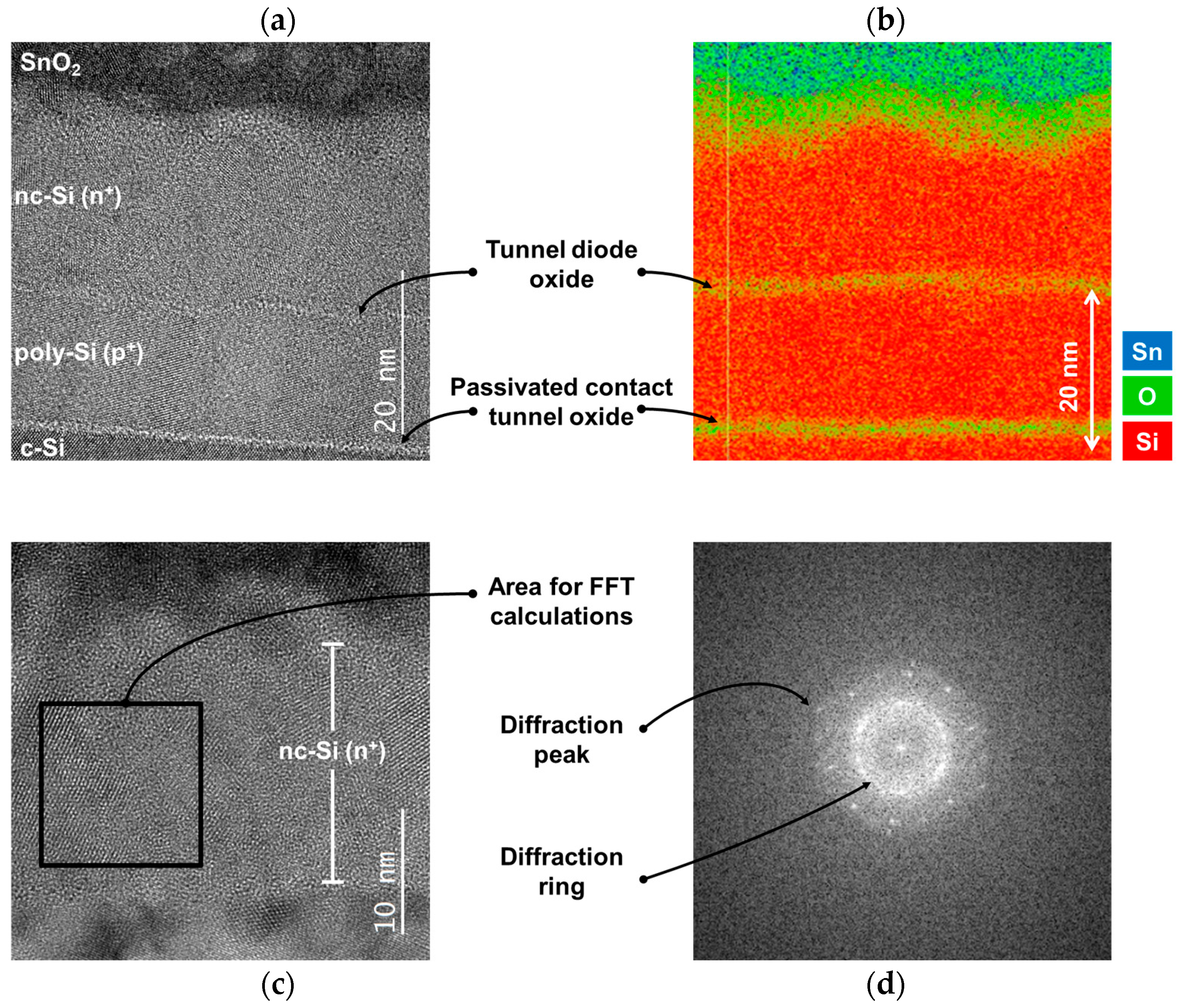
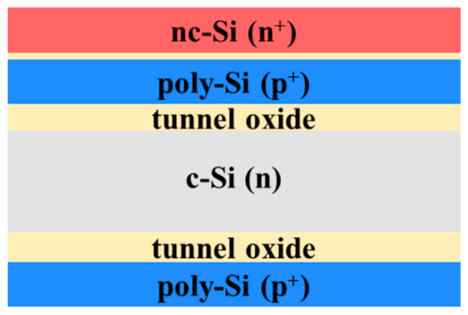
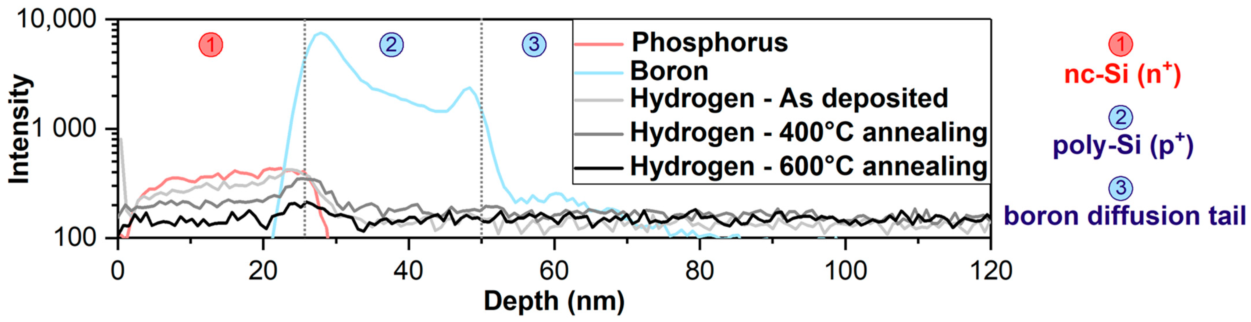
2.1. n+/p+ Tunnel Diode Fabrication

The p-type (n-type) high-temperature passivated contacts are fabricated with ex-situ doping of 15 nm-thick low-pressure chemical-vapor-deposited polycrystalline Si films by B2H6 (PH3) plasma immersion ion implantation. These poly-Si/SiOx stacks are then annealed at 875 °C to ensure crystallization and dopants activation. Passivated contacts’ detailed processing sequence can be found in reference [18]. HRTEM (high-resolution transmission electron microscopy) images of the tunnel diode (Figure 1a) confirm the growth of homogenous polycrystalline Si films with a grain size of about 15 nm, similar to the layer thickness. Electrochemical capacitance-voltage (ECV) profiling (Figure 2a) reveals high doping levels in these p-type poly-Si/SiOx stacks and carrier concentrations above 3 × 10²⁰ holes·cm−3 were measured. This highlights the suitability of our passivated contacts fabrication process for the formation of tunnel diodes.
The nc-Si (n+)/poly-Si (p+) tunnel diodes are then formed with an industrial 2-steps process including, first, wet chemical cleaning of the poly-Si (p+)/SiOx passivated contacts, and second, PECV deposition of the in-situ phosphorous-doped nanocrystalline Si films. During the wet chemical cleaning, the poly-Si (p+) surfaces are deoxidized in an HF/HCl bath and rinsed with ozonized water. It results in the growth of a thin chemical oxide between the n- and p-type layers, as can be seen on energy dispersive X-ray spectroscopy (EDX) imaging of the tunnel diode (Figure 1b). Such an ultra-thin oxide layer is known to prevent dopant inter-diffusion issues [19,20]. Subsequently, 25 nm nc-Si (n+) films are deposited at 230 °C in an industrial PECVD reactor from silane and phosphine precursors dissociated at 0.3 W.cm−2. Figure 1a depicts nc-Si (n+) layers consisting in an amorphous phase, including a mix of small grains with sizes from approximately 2 nm to 10 nm. The diffraction image (Figure 1d) obtained with Fast Fourier Transform (FFT) from nc-Si (n+) (black square region in Figure 1c) shows both diffraction peaks and more or less continuous rings. They are a signature of, respectively, crystalline and amorphous phases. These two phases are intertwined in the 3 spatial dimensions at nanometer scale. ECV measurements (Figure 2a) reveal high doping levels in the nc-Si (n+) layers too, with electrically active dopants concentrations above 2 × 10²⁰ atom.cm-3. Interestingly, high carrier concentrations (>1 × 10²⁰ carrier·cm−3) are measured in both n- and p-type layers even at the junction edges. This demonstrates very sharp junctions with widths below our ECV tool accuracy (WEP CVP21). Thus, our stacks reach both prerequisites for an efficient ESAKI-like tunnel diode [21]. Using SCAPS, we plotted in Figure 2b the band diagram associated with the experimental doping levels measured by ECV [22]. It highlights that such doping levels enable tunneling between the nc-Si (n+) conduction band and poly-Si (p+) valence band through a calculated junction width below 4 nm (between n- and p-type degenerated layers).

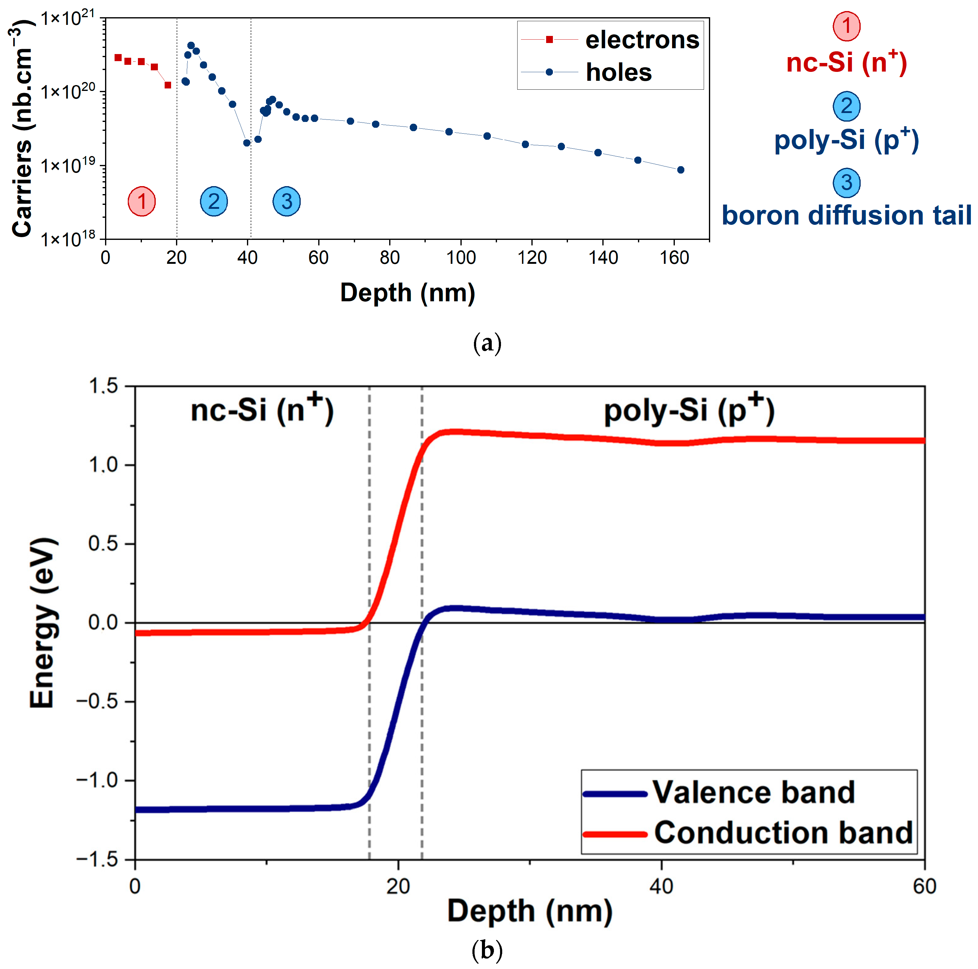
2.2. Passivation Quality Assessment

Specific lifetime samples (Figure 3) featuring double-side poly-Si (p+)/SiOx stacks were produced on n-type CMP (chemical mechanical polishing) wafers. The passivation quality was evaluated via iVOC (implied open circuit voltage) extraction from photoconductance decay measurements with a Sinton tool in transient mode.
Table 1 summarizes the passivation quality (average value of 9 samples) of the precursors with double-side p-type passivated contacts and after nc-Si (n+) deposition on front sides, using the process sequence described in part 2a. Our symmetrical precursors with double-side poly-Si (p+)/SiOx present 691 mV state-of-the-art iVOC values. However, the following deposition of nc-Si (n+) induces an average iVOC degradation of 11.2 mV and enhances variability.
Additionally, we performed 3 different annealings of the tunnel diodes (5 min in lamp oven) and evaluated their impact on the passivation quality (average value of 3 samples). Interestingly, the annealing of the tunnel diode at 400 °C under N2 or N2 + O2 atmospheres allowed passivation recovery of about 8 mV, whereas annealing at 600 °C induced further iVOC losses of 8.4 mV.
Figure 4 presents secondary ion mass spectroscopy (SIMS) measurements of H, P, and B atoms in lifetime samples for tunnel diodes annealed (under N2) up to 600 °C. We plotted the measurement data for P and B independently of the annealing temperature, as the profiles did not change upon annealing. Interestingly, the as-deposited nc-Si (n+) layer contains high hydrogen concentrations, especially close to the surface. Annealing the tunnel diode at 400 °C induces H diffusion (and/or exodiffusion) and depletes the H concentration in the nc-Si (n+) layer, with still high H content at the tunnel diode oxide. Thus, we believe that the passivation recovery observed after such annealing could be explained by hydrogenation of the buried poly-Si/SiOx stack [23]. Annealing at 600 °C led to complete H effusion from the stacks, thus explaining why no passivation gain was observed for such a temperature.
This highlights that the deposition of an nc-Si (n+) layer on a poly-Si (p+)/SiOx stack could provide a double role: formation of the recombination junction and hydrogenation of the buried passivated contacts for bottom cell efficiency improvement.

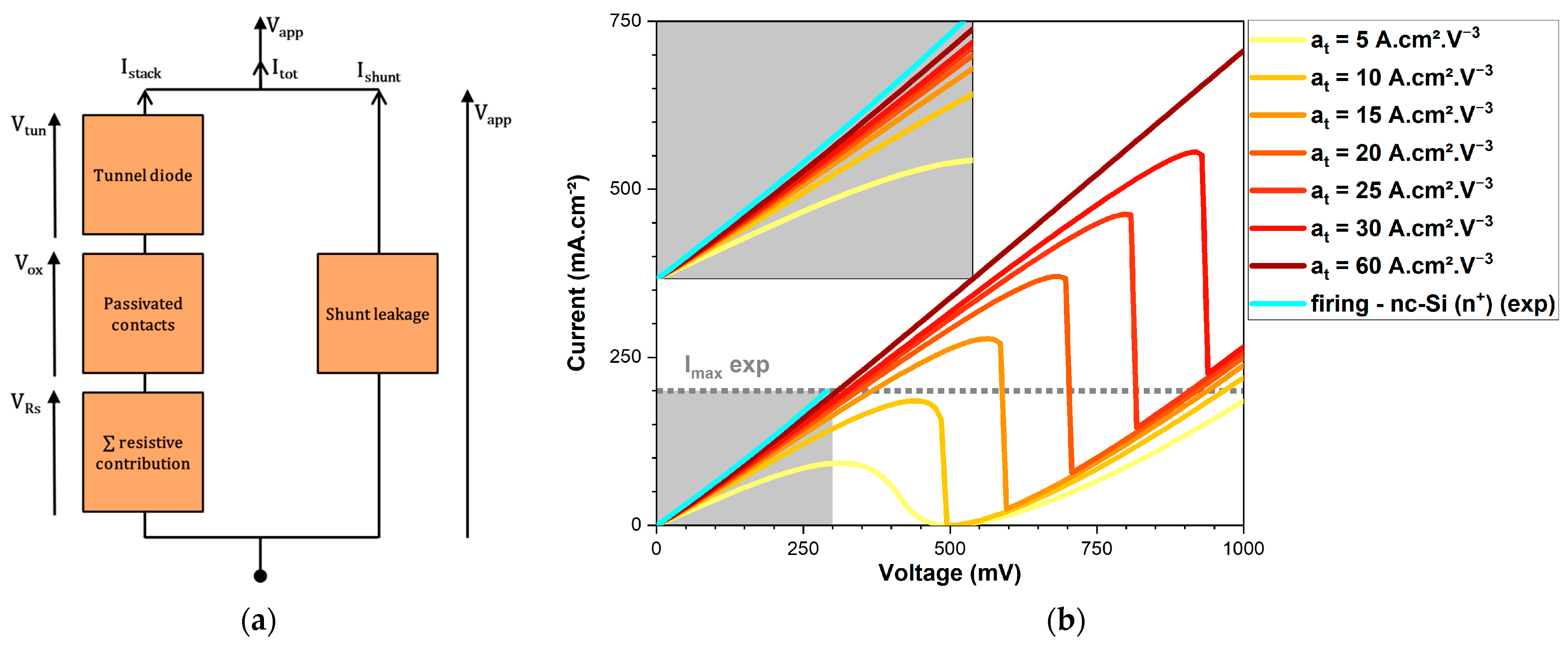
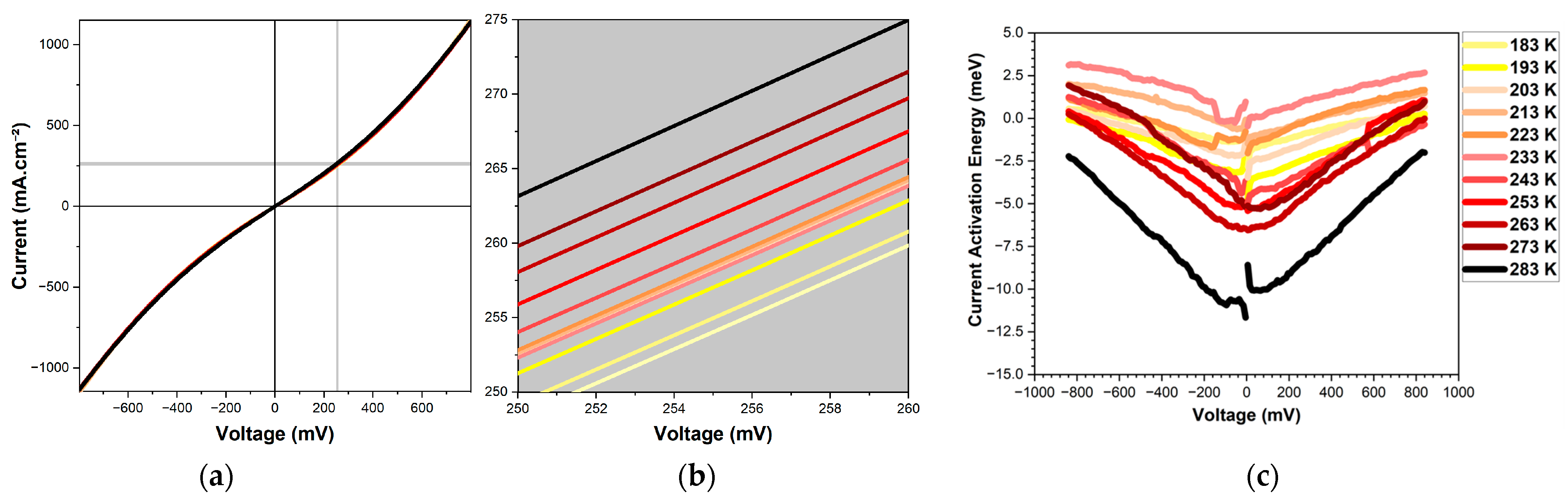
2.3. Conduction Assessment

Samples featuring double-side poly-Si (p+)/SiOx stacks on p-type CMP wafers have been produced for contact resistivity measurements. The tunnel diode is then formed on the front side with nc-Si (n+) deposition according to the process sequence presented in part 2a. (Figure 5a). Additionally, reference samples were fabricated, replacing the nc-Si (n+) PECV deposition step by a 12 nm thick ITOrec physical vapor deposition (PVD) one (Figure 5b). By doing so, we will be able to compare the conductivity of our nc-Si (n+)—poly-Si (p+) tunnel diodes with ITOrec—poly-Si (p+) reference recombination junctions. The test structures were then completed with double side PV deposition of 100 nm thick ITOcontact and 100 nm Ag layers for contact formation.
After passivated contacts fabrication and before nc-Si (n+) or ITOrec deposition, half of the samples underwent an additional firing step of 2 s at 950 °C in a lamp oven. This treatment is known to enable pinhole formation in the SiOx layers to enhance the carrier transport through the oxide. Doing so, we expect the “substrate” to be more conductive, thus enabling more accurate resistivity characterization of the recombination junctions.
Figure 5c presents the dark I–V (current–voltage) measurements of those structures on 25 cm2 samples. The measurement setup imposed current limitations around 200 mA.cm−2. The I–V characteristics present strong non-linearity for the samples without the firing of the passivated contacts independently of the recombination junction (nc-Si (n+) and ITOrec). However, as expected, firing the passivated contacts enabled pinholes formation through the SiOx layers and led to both ohmic I–V characteristics and stack conductivity improvement.
Interestingly, samples with nc-Si (n+) exhibit close I–V characteristics compared with references with ITOrec, indicating equivalent conductivity properties for both approaches. Interestingly, Figure 5c even shows nc-Si (n+)—poly-Si (p+) tunnel diodes slightly more conductive than the ITOrec—poly-Si (p+) reference counterparts.
We developed an electrical calculation model to simulate the dark I–V characteristics of our structures—based on the solution of an equivalent circuit (Figure 6a)—representing the stack of the resistivity samples. We calculated the measured current (ITOT) as a function of the applied voltage (Vapp) using the following electrical components and I–V equations (the detailed numerical approach is presented in Appendix A) [24].
The tunnel oxide films limit the current flowing through the passivated contacts. Thus, for the associated electrical component, the current (Iox) was defined as a function of the voltage (Vox) with the following simplified I–V equation:
I o x = s i g n V a p p   J 0   e s i g n V a p p   V o x   q n   k b   T 1
where J0 is the saturation current, q is the absolute value of the electron charge, n is the ideality factor, kb is the Boltzmann constant, and T is the absolute temperature.
The tunnel diode is expected to enable band-to-band tunneling, and the following empirical equation was used:
I t u n = a t   V t u n   V d d V t u n 2
where Itun is the current flowing through the tunnel diode, at is the tunnel diode pre-factor, Vtun is the voltage across the tunnel diode, and qVdd is the energy between n-type conduction and p-type valence bands.
The other interfaces and bulk materials are assumed to have ohmic I–V characteristics and are modeled together in a single electrical component with the following equation:
I R s = V R s R s
where IRs is the current flowing through the component, VRs is the voltage across the component, and Rs is a global series resistance.
A component in parallel of this stack accounts for shunts leakage through the structure and is modeled with:
I s h u n t = V a p p R s h u n t
where Ishunt is the current, Vapp is the voltage, and Rshunt is the shunt resistance.
First, we ran electrical calculations without taking into account any tunnel diodes in the modeled stack in order to determine relevant parameters for Equations (1), (3), and (4). The parameters presented in Table 2 led to efficient fits between the simulated and experimental I–V characteristics (Figure 7) and were used for the following calculations.
Figure 6b presents calculation results for simulations including the tunnel diode in the modeled stack. The tunnel diode conductivity has been varied by changing the tunnel diode prefactor (at) value. It can be seen that the peak-to-valley behavior characteristic of tunnel diodes is displaced for larger values of at. For values above 10 A·cm2·V−3, this behavior appears for currents higher than our setup limitation. Thus, transparent tunnel diodes on experimental I–V characteristics are proof of highly conductive diodes. Interestingly, when the tunnel diode resistivity is increased (at value decreased), the total slope of the dark I–V characteristic decreases, even for low current values. Thus, comparing the slope of our tunnel diodes with one of reference recombination junctions seems relevant to assess equivalent conductivity properties for both approaches.
Figure 8a,b present the dark I–V characteristics of the tunnel diode (Figure 5a) at different temperatures on 0.08 cm2 samples under liquefied N2 cooling (Janis ST-500, Keithley 4200-SCS). At 250 mV, we observe around 5%rel current losses (15 mA·cm2) over a 100 °C temperature variation. Thus, the current exhibits extremely low dependency on the measurement temperature. Figure 8c presents the current activation energy calculated with Equation (5) and reveals Ea below 10 meV. Such a low activation energy confirms a high band-to-band tunneling current [24,25].
E a = d l n I d q k b   T      
where Ea is the activation energy, I the current, q the absolute value of the electron charge, kb the Boltzmann constant, and T the absolute temperature.

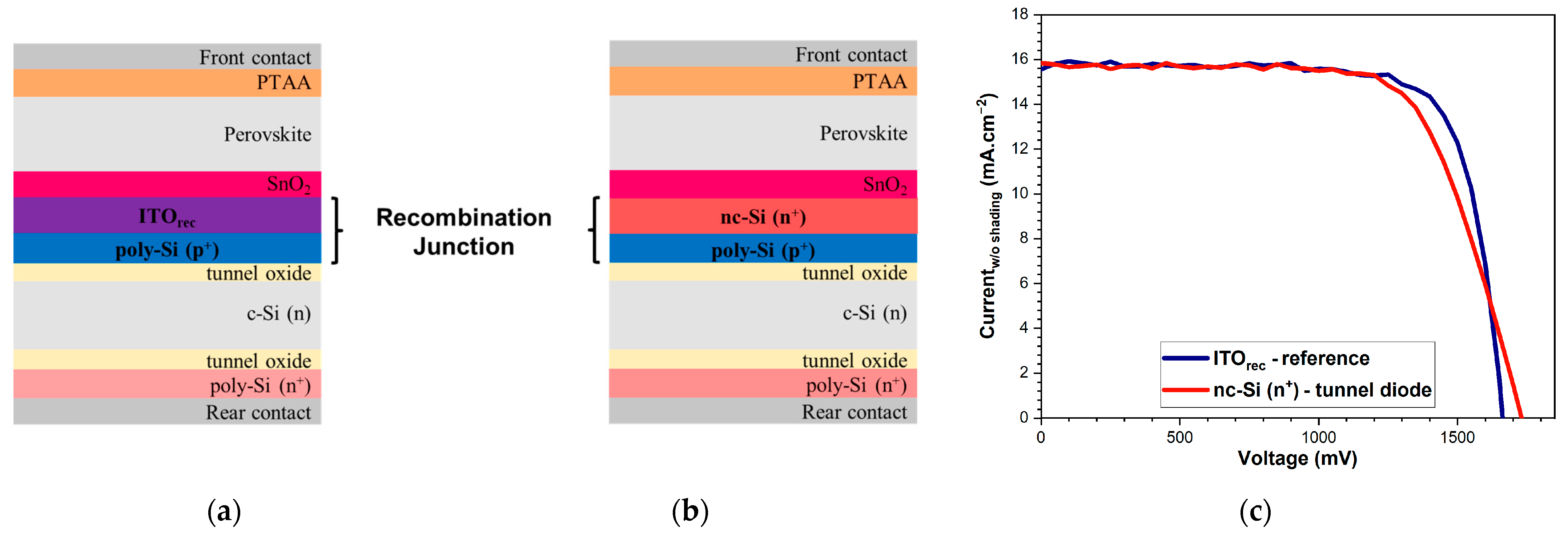
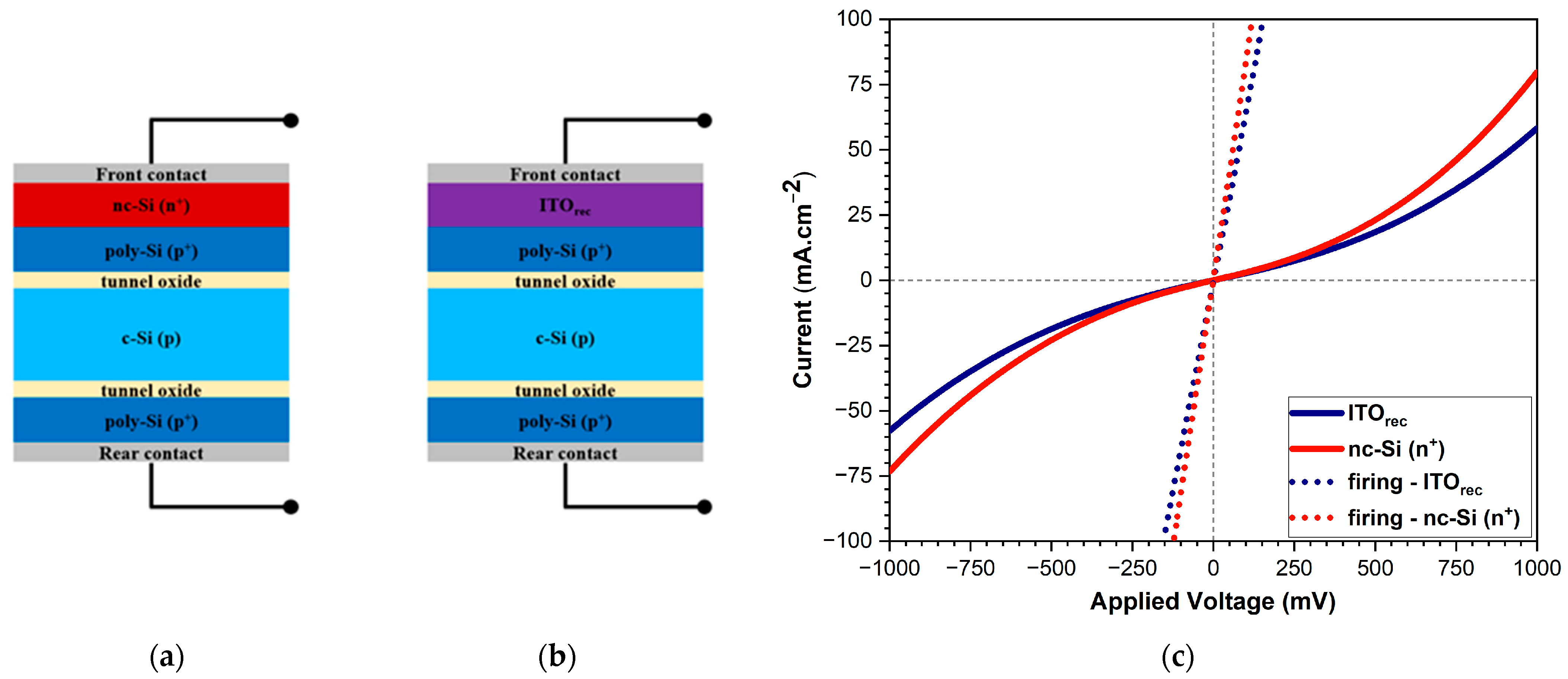
2.4. Tandem Integration

To complete the study, 9 cm2 nip Pk/c-Si tandem devices integrating tunnel diodes recombination junctions were fabricated (Figure 9b) and compared with reference devices featuring ITOrec-based ones instead (Figure 9a). The bottom cells consist in CMP c-Si cells (M2 format, 244.26 cm2), featuring double poly-Si/SiOx stacks, phosphorus-doped on the rear side, and boron-doped on the front side. The recombination junction was then built on the front side with 25 nm nc-Si (n+) PECV deposition (tunnel diode) according to the process described in part 2a or with 12 nm ITOrec PV deposition (reference). To ensure optimal wettability of the bottom cell front surface before Pk top cell spin coating, a UV-Ozone treatment was performed for 30 min for reference devices presenting ITOrec. However, if such a treatment is a reference on ITOrec films, it could lead to the degradation of the tunnel diodes Si layers due to unwanted surface oxidation [26,27]. Thus, samples with nc-Si (n+) were integrated without UV-Ozone surface treatment. The 9 cm2 Pk top cell was then fabricated with spin coating of 30 nm SnO2 (electron transport layer), 300 nm MaPBI3 (methylammonium lead iodide, absorber), and 50 nm PTAA (poly[bis(4-phenyl)(2,4,6-trimethylphenyl)amine, hole transport layer). Finally, the devices were completed, and contacts were formed with double side PV deposition of 100 nm ITOcontact and evaporation of 200 nm Ag layers (full area on the rear side and patterned on the front side).
Figure 9c shows the AM1.5 (Air Mass 1.5) devices’ I–V characteristics and Table 3 shows the associated I–V parameters’ average values. Integration of the silicon tunnel diode in nip Pk/c-Si tandem devices led to a champion device presenting 19.0% PCE and 70% FF. Obtaining high Voc and fill factor values confirm the tunnel diodes provide efficient carrier recombination current between both subcells.
Devices with tunnel diode (nc-Si (n+)) recombination junctions show an average of 1.1%abs PCE and 6.3%abs FF losses compared with those of references (ITOrec). These losses are caused by non-optimized SnO2—nc-Si (n+) interfaces leading to internal series resistances, therefore limiting our devices’ fill factors and efficiencies values. We attributed the high SnO2—nc-Si (n+) resistivity to the growth of a parasitic interfacial SiOx layer.
Therefore, the tunnel diode presents high recombination tunneling current and leads to functional Pk/c-Si solar cells with high FF values. Thus, they represent an indium-free alternative to ITOrec-based recombination junctions. However, the contact between the bottom cell last silicon layer (nc-Si (n+) and top cell ETL still has to be improved by either reducing the interface oxidation sensitivity or by exploring the use of other ETL materials.

3. Conclusions

Silicon tunnel diodes have already been investigated for application as recombination junctions in Pk/c-Si tandem devices for pin structures with SHJ or TOPCon bottom cells and for nip structures with SHJ bottom cells. Here, we studied n/p tunnel diodes (nip structure) to reveal their potential to form efficient recombination junctions on TOPCon bottom cells too.
We showed that an industrially adapted one-step process featuring an nc-Si (n+) layer PECV deposition on a boron-doped passivated contacts enables the formation of a well-crystalized and highly doped n+/p+ tunnel diode reaching both ESAKI requirements for an efficient tunnel diode (strong active doping levels and sharp junction). The nc-Si (n+)/poly-Si (p+)/SiOx stacks show good passivation of the c-Si bottom cell (iVoc = 680.1 mV). A subsequent annealing step at 400 °C leads to an 8.0 mV gain attributed to hydrogenation of the passivated contacts by the H-rich nc-Si (n+) layer. Dark I–V measurements of resistivity structures highlight low resistivity nc-Si (n+)—poly-Si (p+) tunnel diodes. They even seem more conductive than the ITOrec—poly-Si (p+) reference recombination junction. The tunnel diode presents both high surface passivation quality and good conductivity, and thus, is an efficient alternative to ITOrec-based recombination junctions.
The fabrication of 9 cm2 Pk/Si nip tandem devices integrating tunnel diodes as recombination junctions enables fill factors of up to 70% and efficiencies of up to 18.8%. This assesses efficient carrier recombination between subcells. However, such cells still present 6.3%abs fill factor losses compared with references with ITOrec-based recombination junctions. This is likely due to internal series resistances coming from a non-optimized SnO2—nc-Si (n+) interface.

Author Contributions

Conceptualization, B.M. and T.D.; methodology, B.M. and T.D.; software, B.M. and Q.R.; writing—original draft preparation, B.M.; writing—review and editing, T.D., Q.R., S.D. and A.K.; supervision, S.D. and A.K. All authors have read and agreed to the published version of the manuscript.

Funding

This research received no external funding.

Data Availability Statement

The data can be accessed upon request from any of the authors.

Acknowledgments

We would like to thank François Saint-Antonin and Julien Lavie from CEA Liten for the measurements and analysis of respectively TEM and SIMS characterizations. This work, carried out on the Platform for Nanocharacterisation (PFNC), was supported by the “Recherches Technologiques de Base” program of the French National Research Agency (ANR).

Conflicts of Interest

The authors declare no conflict of interest.

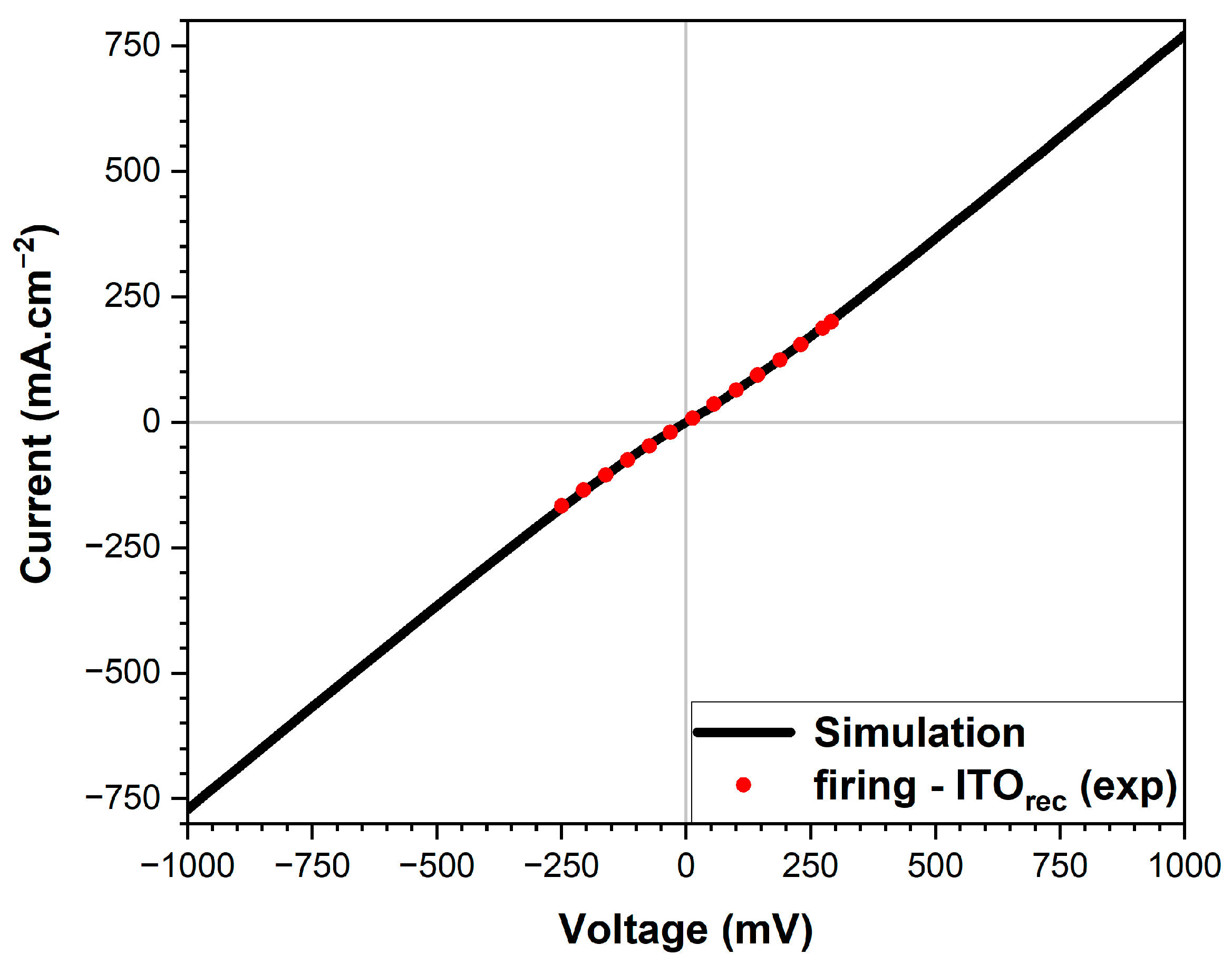
Appendix A. Dark IV Simulation of Resistivity Samples

The resistivity samples equivalent electrical circuit presented in Figure 7a show a stack of 3 electrical components in series. Thus, from the Equations (1)–(3), we can write the following equations:
I t u n = I o x = I R s
V t u n + V o x + V R s = V a p p
which lead to the system:
I R s I o x = 0 I o x I t u n = 0 V t u n + V o x + V R s V a p p = 0
This equation system can be solved with the Newton–Raphson numerical method [28]. Writing the vector F in the function of the vector V,
V = V R s V o x V t u n
F V R s V o x V t u n = I R s I o x I o x I t u n V R s + V o x + V t u n V a p p
F = s i g n V a p p   J 0   e s i g n V a p p   V o x   q n   k b   T 1 + V R s R s a t   V t u n   V d d V t u n 2 + s i g n V a p p   J 0   e s i g n V a p p   V o x   q n   k b   T 1 V a p p + V R s + V o x + V t u n
The Jacobian J associated with the F function is given by:
  J = d F 1 d V R s d F 1 d V o x d F 1 d V t u n d F 2 d V R s d F 2 d V o x d F 2 d V t u n d F 3 d V R s d F 3 d V o x d F 3 d V t u n = d F 1 d V R s d F 1 d V o x 0 0 d F 2 d V o x d F 2 d V t u n 1 1 1
J = 1 R s s i g n V a p p   J 0   e s i g n V a p p   V o x   q n   k b   T n   k b   T 0 0 s i g n V a p p   J 0   e s i g n V a p p   V o x   q n   k b   T n   k b   T a t   V t u n   2 V d d + 2 V t u n a t   V d d V n p 2 1 1 1
The algorithm toward the solution V is iterative and the relation between an iteration k and an iteration k + 1 is written as:
V k + 1 = V k + J 1 F V k

References

  1. International Technology Roadmap for Photovoltaic (ITRPV)—vdma.org—VDMA. Available online: https://www.vdma.org/international-technology-roadmap-photovoltaic (accessed on 23 February 2023).
  2. At 26.81%, LONGi Sets a New World Record Efficiency for Silicon Solar Cells, Longi. Available online: https://www.longi.com/en/news/propelling-the-transformation// (accessed on 23 February 2023).
  3. JinkoSolar’s High-Efficiency N-Type Monocrystalline Silicon Solar Cell Sets New World Record with Maximum Conversion Efficiency of 25.7%|JinkoSolar. Available online: https://ir.jinkosolar.com/news-releases/news-release-details/jinkosolars-high-efficiency-n-type-monocrystalline-silicon-0 (accessed on 23 February 2023).
  4. Hollemann, C.; Haase, F.; Schäfer, S.; Krügener, J.; Brendel, R.; Peibst, R. 26.1%-efficient POLO-IBC cells: Quantification of electrical and optical loss mechanisms. Prog. Photovolt. Res. Appl. 2019, 27, 950–958. [Google Scholar] [CrossRef]
  5. Richter, A.; Hermle, M.; Glunz, S.W. Reassessment of the Limiting Efficiency for Crystalline Silicon Solar Cells. IEEE J. Photovolt. 2013, 3, 1184–1191. [Google Scholar] [CrossRef]
  6. NREL. Best Research-Cell Efficiency Chart. Available online: https://www.nrel.gov/pv/cell-efficiency.html (accessed on 23 February 2023).
  7. Li, X. High-Efficiency Si Solar Cell Including Tunnel Junction for Tandem Photovoltaic Cells. Ph.D. Thesis, Université de Lyon, Lyon, France, 2021; p. 155. [Google Scholar]
  8. Helmholtz-Zentrum Berlin. World Record Back at HZB: Tandem Solar Cell Achieves 32.5 Percent Efficiency, HZB Website. Available online: https://www.helmholtz-berlin.de/pubbin/news_seite?nid=24348;sprache=en (accessed on 23 February 2023).
  9. Leijtens, T.; Bush, K.A.; Prasanna, R.; McGehee, M.D. Opportunities and challenges for tandem solar cells using metal halide perovskite semiconductors. Nat. Energy 2018, 3, 10. [Google Scholar] [CrossRef]
  10. Communication from the Commission to The European Parliament; The Council; The European Economic and Social Committee; The Committee of The Regions. Critical Raw Materials Resilience: Charting a Path towards greater Security and Sustainability. 2020. Available online: https://eur-lex.europa.eu/legal-content/EN/TXT/?uri=CELEX:52020DC0474 (accessed on 28 April 2023).
  11. Kim, M.; Zhang, Y.; Verlinden, P.; Hallam, B. Towards sustainable silicon PV manufacturing at the terawatt level. AIP Conf. Proc. 2022, 2487, 090001. [Google Scholar] [CrossRef]
  12. De Bastiani, M.; Subbiah, A.S.; Aydin, E.; Isikgor, F.H.; Allen, T.G.; De Wolf, S. Recombination junctions for efficient monolithic perovskite-based tandem solar cells: Physical principles, properties, processing and prospects. Mater. Horiz. 2020, 7, 2791–2809. [Google Scholar] [CrossRef]
  13. Chi, W.; Banerjee, S.K.; Jayawardena, K.G.D.I.; Silva, S.R.P.; Seok, S.I. Perovskite/Silicon Tandem Solar Cells: Choice of Bottom Devices and Recombination Layers. ACS Energy Lett. 2023, 8, 1535–1550. [Google Scholar] [CrossRef]
  14. Shen, H.; Walter, D.; Wu, Y.; Fong, K.C.; Jacobs, D.A.; Duong, T.; Peng, J.; Weber, K.; White, T.P.; Catchpole, K.R. Monolithic Perovskite/Si Tandem Solar Cells: Pathways to Over 30% Efficiency. Adv. Energy Mater. 2019, 10, 1902840. [Google Scholar] [CrossRef]
  15. Nogay, G.; Sahli, F.; Werner, J.; Monnard, R.; Boccard, M.; Despeisse, M.; Haug, F.-J.; Jeangros, Q.; Ingenito, A.; Ballif, C. 25.1%-Efficient Monolithic Perovskite/Silicon Tandem Solar Cell Based on a p-type Monocrystalline Textured Silicon Wafer and High-Temperature Passivating Contacts. ACS Energy Lett. 2019, 4, 844–845. [Google Scholar] [CrossRef]
  16. Sahli, F.; Kamino, B.A.; Werner, J.; Bräuninger, M.; Paviet-Salomon, B.; Barraud, L.; Monnard, R.; Seif, J.P.; Tomasi, A.; Jeangros, Q.; et al. Improved Optics in Monolithic Perovskite/Silicon Tandem Solar Cells with a Nanocrystalline Silicon Recombination Junction. Adv. Energy Mater. 2018, 8, 1701609. [Google Scholar] [CrossRef]
  17. Sahli, F.; Werner, J.; Kamino, B.A.; Bräuninger, M.; Monnard, R.; Paviet-Salomon, B.; Barraud, L.; Ding, L.; Leon, J.J.D.; Sacchetto, D.; et al. Fully textured monolithic perovskite/silicon tandem solar cells with 25.2% power conversion efficiency. Nat. Mater. 2018, 17, 9. [Google Scholar] [CrossRef] [PubMed]
  18. Seron, C.; Desrues, T.; Jay, F.; Lanterne, A.; Torregrosa, F.; Borvon, G.; Rafhay, Q.; Kaminski, A.; Dubois, S. Hydrogenation of sputtered ZnO:Al layers for double side poly-Si/SiOx solar cells. EPJ Photovolt. 2022, 13, 8. [Google Scholar] [CrossRef]
  19. Luderer, C.; Penn, M.; Reichel, C.; Feldmann, F.; Goldschmidt, J.C.; Richter, S.; Hahnel, A.; Naumann, V.; Bivour, M.; Hermle, M. Controlling Diffusion in Poly-Si Tunneling Junctions for Monolithic Perovskite/Silicon Tandem Solar Cells. IEEE J. Photovolt. 2021, 11, 1395–1402. [Google Scholar] [CrossRef]
  20. Penn, M.; Luderer, C.; Reichel, C.; Goldschmidt, J.C.; Feldmann, F.; Bivour, M.; Hermle, M. Passivating Poly-Si Tunnel Junctions with Oxide-based Diffusion Barriers for Interconnection in Perovskite/Si Tandem Solar Cells. AIP Conf. Proc. 2022, 2487, 4. [Google Scholar]
  21. Esaki, L. New Phenomenon in Narrow Germaniump−nJunctions. Phys. Rev. 1958, 109, 603–604. [Google Scholar] [CrossRef]
  22. Burgelman, M.; Nollet, P.; Degrave, S. Modelling polycrystalline semiconductor solar cells. Thin Solid Film. 2000, 361–362, 527–532. [Google Scholar] [CrossRef]
  23. Song, L.; Hu, Z.; Lin, D.; Yang, D.; Yu, X. Progress of hydrogenation engineering in crystalline silicon solar cells: A review. J. Phys. D Appl. Phys. 2022, 55, 453002. [Google Scholar] [CrossRef]
  24. Sze, S.M.; Lee, M.K. Semiconductor Devices, Physics and Technology, 3rd ed.; Wiley: Hoboken, NJ, USA, 2012. [Google Scholar]
  25. Arunachalam, B.; Rafhay, Q.; Roy, D.; Kaminski-Cachopo, A. Simulation Study of High-Speed Ge Photodetector Dark and Light Current Degradation. IEEE Trans. Device Mater. Reliab. 2022, 22, 410–416. [Google Scholar] [CrossRef]
  26. Jeon, H.; Choi, H.; Cho, Y.S.; Ryoo, K.K.; Jung, S.D. Effects of UV/O3 and SC1 Steps for the HF Last Silicon Wafer Cleaning. MRS Online Proc. Libr. 1995, 386, 297–302. [Google Scholar] [CrossRef]
  27. Moldovan, A.; Feldmann, F.; Krugel, G.; Zimmer, M.; Rentsch, J.; Hermle, M.; Roth-Fölsch, A.; Kaufmann, K.; Hagendorf, C. Simple Cleaning and Conditioning of Silicon Surfaces with UV/Ozone Sources. Energy Procedia 2014, 55, 834–844. [Google Scholar] [CrossRef]
  28. Press, W.H. (Ed.) FORTRAN Numerical Recipes, 2nd ed.; Cambridge University Press: Cambridge, NY, USA, 1996. [Google Scholar]
Figure 1. (a). HRTEM and (b). EDX imaging of the nc-Si (n+)/poly-Si (p+) tunnel diode and (d). fast Fourier transform (FFT) diffraction analysis in nc-Si (n+) calculated in area circled in (c).
Energies 16 04346 g001
Figure 2. (a). ECV of nc-Si (n+)/poly-Si (p+) tunnel diode and (b). the associated band diagram calculated with SCAPS.
Energies 16 04346 g002
Figure 3. Lifetime samples.
Energies 16 04346 g003
Figure 4. SIMS measurement of tunnel diode for different annealing temperatures.
Energies 16 04346 g004
Figure 5. Scheme of the resistivity samples with (a). nc-Si (n+) or (b). ITOrec and (c). the corresponding dark I–V characteristics.
Energies 16 04346 g005
Figure 6. (a). Electrical scheme of resistivity samples and (b). the associated simulation and experimental results.
Energies 16 04346 g006
Figure 7. Simulated I–V characteristics versus experimental results.
Energies 16 04346 g007
Figure 8. (a). I–V characteristic of the tunnel diode (Figure 5a) with (b). focus on the grey area and (c). the current activation energy for different temperatures.
Energies 16 04346 g008
Figure 9. Tandem devices with (a). ITO-based and (b). tunnel diode recombination junctions and (c). the AM1.5 I–V characteristics.
Energies 16 04346 g009
Table 1. iVOC of lifetime samples at different processing steps (ΔiVOC = iVOC, post annealing − iVOC, pre annealing).
StepsPoly-Si (p+) Formation (Both Sides)nc-Si (n+) Deposition (Front Side)400 °C
(N2)
600 °C
(N2)
400 °C
(N2 + O2)
iVOC (mV)691.3 (±3.7)680.1 (±10.4)681.7 (±1.0)
ΔiVOC = +7.3
671.7 (±3.6)
ΔiVOC = −8.4
688.7 (±3.4)
ΔiVOC = +8.0
Table 2. Parameters used for Equations (1), (3), and (4).
RSRshuntJ0n
1.20 Ω·cm260 Ω·cm20.1 A·cm−21.3
Table 3. AM1.5 IV parameters for Pk/c-Si tandem devices with different RJ (average of 3 cells).
InterlayerVOC (mV)ISC (mA.cm−2)FF (%)PCE (%)
ITOrec1676 ± 1915.7 ± 0.275.6 ± 0.8 19.9 ± 0.2
nc-Si (n+)1688 ± 4016.1 ± 0.869.3 ± 0.818.8 ± 0.4
Disclaimer/Publisher’s Note: The statements, opinions and data contained in all publications are solely those of the individual author(s) and contributor(s) and not of MDPI and/or the editor(s). MDPI and/or the editor(s) disclaim responsibility for any injury to people or property resulting from any ideas, methods, instructions or products referred to in the content.

