Abstract
Single-phase inverters are widely employed in renewable energy applications. However, their inherent 2ω-ripple power can substantially affect system performance, leading to fluctuations in the maximum power points (MPP) of photovoltaic (PV) systems and shortening the lifespans of fuel cell (FC) systems. To alleviate input ripple, a three-leg quasi-Z-source inverter (QZSI) and its associated control strategy are proposed. The QZSI consists of a quasi-Z-source network, an H-Bridge inverter, and an active power filter (APF). The active filtering structure comprises filtering capacitors and the third bridge leg. The proposed control strategy consists of three loops: open-loop simple boost control, output voltage control, and 2ω-ripple suppression control. Open-loop simple boost control is utilized for shoot-through state modulation, output voltage control is applied to the two bridge-legs of the H-Bridge, and the additional third bridge-leg adopts a quasi-PR control (QPR) method that injects specific frequency harmonic voltage and suppresses newly generated low-frequency components of the input current. This method effectively avoids the drawbacks of utilizing passive filtering strategies, such as high-value impedance networks, low power density, and weak system stability. A simulation platform of 300W 144VDC/110VAC50Hz is constructed. The simulation results indicate that the addition of the third bridge leg under full load conditions reduces the input-side inductor current ripple ΔI from 1.89 A with passive filtering to 0.513 A, representing a reduction of 72.86%. The second harmonic ripple of the input current is reduced from 18.2% to 4.5%, and the fourth harmonic ripple is reduced from 16.5% to 2.1%. The DC bus voltage ripple ΔVPN falls from 70.75 V to 6.54 V, representing a reduction of 90.76%. The Total Harmonic Distortion (THD) of the output voltage and current are both less than 1%. The simulation results validated the feasibility of the proposed approach.
1. Introduction
It is widely recognized that the DC side of single-phase inverter systems can generate double frequency (2ω) current ripple as a result of pulsating power [1]. The 2ω ripple power can exert harmonic stresses on the DC side of the inverter, causing overheating and inefficiencies, as well as significantly impacting system functionality [2]. In photovoltaic power generation applications, low-frequency pulsating currents can affect the Maximum Power Point Tracking (MPPT) of the circuit and the energy utilization of the photovoltaic panel, ultimately resulting in a reduction in the power generation efficiency of photovoltaic power generation systems [3,4,5,6,7]. In addition, for the chargers of electric vehicles, in the Vehicle-to-Grid (V2G) operation mode, the secondary ripple component on the DC side is more severe, further reducing the life and performance of the battery pack [8,9]. For three-phase systems, in the event of an asymmetrical fault, the AC side will also produce 2ω ripple, and the 2ω ripple can seriously affect the DC bus voltage and even the generation side. Therefore, research efforts focused on suppressing low-frequency pulsating power in new energy supply systems as an important research direction. The methods of suppressing 2ω ripple in traditional inverters are usually divided into passive filtering and active filtering [10,11].
Passive techniques involve the use of inductors and capacitors as LC passive filters on the DC side to absorb low-frequency ripple. The passive power decoupling technology employed in traditional voltage-source and current-source inverters does not require additional active switches, making it simple to implement with straightforward control. Voltage-source inverters usually employ large-capacity electrolytic capacitors to suppress high-frequency switching ripple voltage and low-frequency ripple voltage [12]. However, the equivalent series resistance of the electrolytic capacitor leads to power loss during operation, which can cause its temperature to rise and significantly shorten the lifespan of the electrolytic capacitor. Two-stage inverters are widely utilized in applications where the input voltage on the DC side undergoes significant changes, or when there is a substantial difference between the input voltage on the DC side and the output voltage on the AC side. Such inverters comprise a DC-DC converter in the front stage and an inverter in the rear stage. However, ripple power may generate a secondary ripple current in the input current of the rear-stage inverter. This secondary ripple current flows back to the front-stage DC-DC converter and the DC input source, increasing the current stress of the power switches and resulting in power loss. Typically, a DC-side electrolytic capacitor is utilized to absorb the secondary ripple current in parallel, which places significant demands on the capacitor. To mitigate this issue, the authors of [13] proposed a current compensation control scheme with repetitive control. Additionally, [14] and [15] propose different control methods to suppress the secondary ripple current of the Two-Stage Power Factor Correction (PFC) converter and AC/DC/AC converter, respectively. The impedance-source converters are widely used in various fields, such as fuel cells, photovoltaic arrays, and electric vehicles [16,17,18]. However, there is secondary ripple power on the DC side of single-phase impedance-source inverters, and impedance-source converters generally require a large impedance-source network to filter out low-frequency ripple [16,19,20]. To decrease the demand for electrolytic capacitors, impedance-source inverters typically optimize the impedance-source network parameters in terms of passive power decoupling topology. The authors of [21] proposed an effective method for suppressing secondary ripple that reduces the capacitor requirements for single-phase Z-source/quasi-Z-source inverters, storing secondary ripple energy in C1 and C2. Compared to traditional quasi-Z-source inverter photovoltaic power generation systems, although the capacitance value is reduced, the voltage stress of the switch increases slightly, leading to a decrease in efficiency.
Active filtering is the method of using active filters usually composed of power switches and energy storage elements to buffer low-frequency ripple [22,23,24]. To reduce the demand for DC side inductors and capacitors, a separate active power buffer can be designed. Low-frequency ripple power can be handled using additional power electronic devices and energy storage elements. Since the voltage or current of the storage element in the separate active power buffer can be controlled independently, the volume of the power buffer can be reduced through increasing the AC variation in the voltage or current of the storage element. The authors of [25] integrated the single-phase switched boost inverter (SBI) with a separate boost-type active power buffer to reduce passive components on the switch impedance network. The authors of [26] proposed an Active Low-Frequency Ripple Control Device (ALFRCD) and control method for Building-Integrated Photovoltaic (BIPV) systems, which reduces the use of electrolytic capacitors and improves the lifespan and reliability of the photovoltaic system through introducing a boost-type active low-ripple control device. The authors of [22] proposed three control methods for the voltage and ripple of the energy storage capacitor of the active power buffer, including voltage set-point control, ripple ratio control, and minimum voltage set-point control. Buck-boost-type active power buffers have wide voltage adjustment characteristics, and there is no upper limit on the voltage set-point of the energy storage capacitor; however, when it is much lower than the DC bus voltage, it may affect the effectiveness of the secondary ripple suppression. In addition, to suppress the influence of dc-link voltage ripple on the back-stage DAB, the authors of [27] proposed a feedback linearization control strategy; however, this technique is designed for two-stage converters and cannot achieve good ripple suppression for single-stage inverters.
However, conventional inverters contain only one degree of control freedom, and when the desired AC side voltage amplitude is higher than the given DC voltage value, a DC-DC converter must be integrated to form a two-stage structure to meet the demand [28].
Compared to conventional inverters, the quasi-Z-source inverter (QZSI) [29] offers several advantages that make it an attractive alternative. Firstly, the QZSI has two independent degrees of control freedom—the shoot-through duty cycle and the modulation—providing greater flexibility in controlling the output. Secondly, its unique impedance network structure allows for both boost and buck functions of a DC-DC converter, resulting in a single-stage system that is more cost effective. Thirdly, the QZSI permits bridge leg shoot-through and exhibits stronger anti-electromagnetic interference (EMI) capability. These features make the QZSI a more appealing option for power electronics applications. Similar to traditional inverters, QZSI can also absorb 2ω ripple using passive filtering techniques. [30,31] analyzed the relationship between the 2ω current and capacitor voltage of the impedance network and the impedance network parameters based on the small signal model. The authors of [30] provided a principle for designing LC parameters using the allowable ripple percentage of inductor current and capacitor voltage under symmetric parameter conditions. The authors of [31] stated that a higher percentage of ripple is needed to meet the demand under asymmetric parameters. However, the method proposed in [30,31] requires large-capacity capacitor and inductor impedance networks, which will not only lead to large volume, heavy weight, and high cost of inverters, but will also reduce the efficiency and reliability of the system.
The authors of [32,33] proposed methods to reduce the 2ω ripple through adjusting the shoot-through duty cycle. The authors of [32] proposed a current damping control method, which can completely eliminate the low-frequency ripple in the inductor current of the impedance network. However, this method requires a complex and sophisticated control system. On the other hand, [33] presented a hybrid pulse width modulation technique that can significantly reduce the required inductance and capacitance values. Nevertheless, the system must be paralleled with a large-capacity DC power supply terminal capacitor.
To minimize the 2ω ripple on the DC input side without increasing the parameters of the impedance network, this paper proposes a novel single-phase three-leg QZSI topology. This topology is based on the active filtering techniques of traditional inverters and injects harmonic voltage into an additional third bridge leg to buffer low-frequency pulsating power, effectively suppressing input current ripple. Compared with the passive filtering suppression method, the additional power switching device used in this approach is smaller in size and weight. Furthermore, the impedance network only needs to avoid the switching frequency ripple setting, which significantly improves the power density of the inverter. The paper is organized as follows: Section 2 introduces the circuit topology and ripple suppression principle of single-phase three-leg QZSI, Section 3 discusses the control strategy of the system, Section 4 designs the system parameters, Section 5 shows simulation results, and Section 6 concludes this work.
2. Circuit Topology and Operating Principle of the Proposed Inverter
2.1. Traditional Quasi-Z-Source Inverter and the Analysis of Its Secondary Ripple
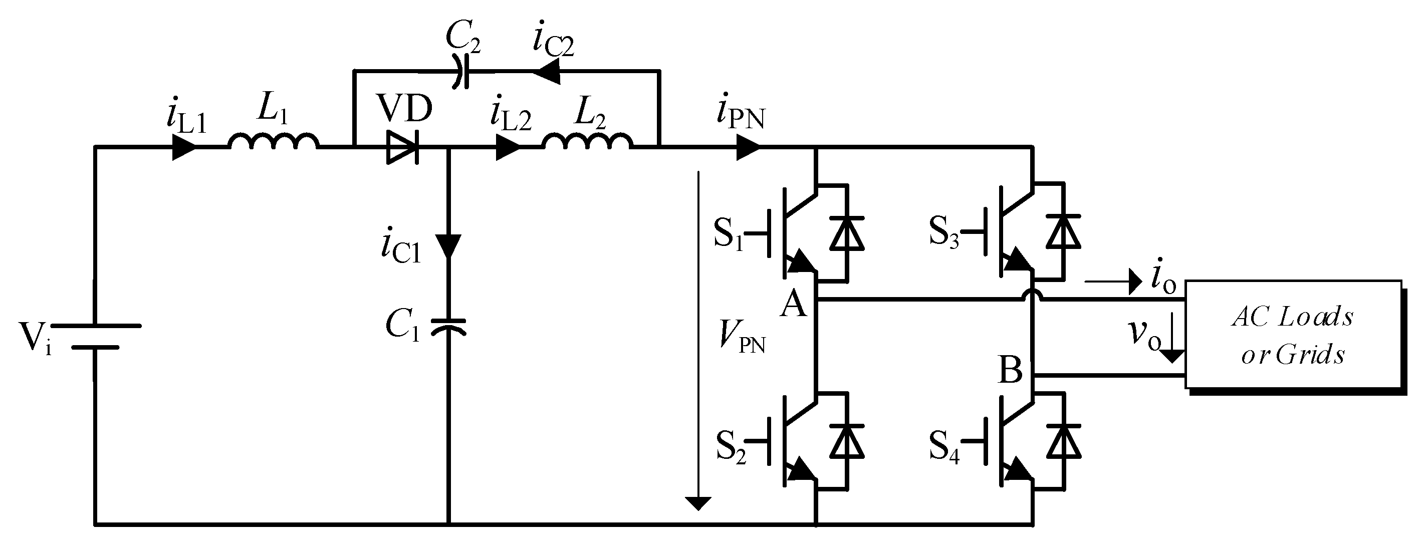
The traditional single-phase QZSI contains two bridge legs, and there are two operating modes: the shoot-through state and the non-shoot-through state. The circuit topology is shown in Figure 1.

Figure 1.
Circuit topology of traditional single-phase quasi-Z-source inverter.
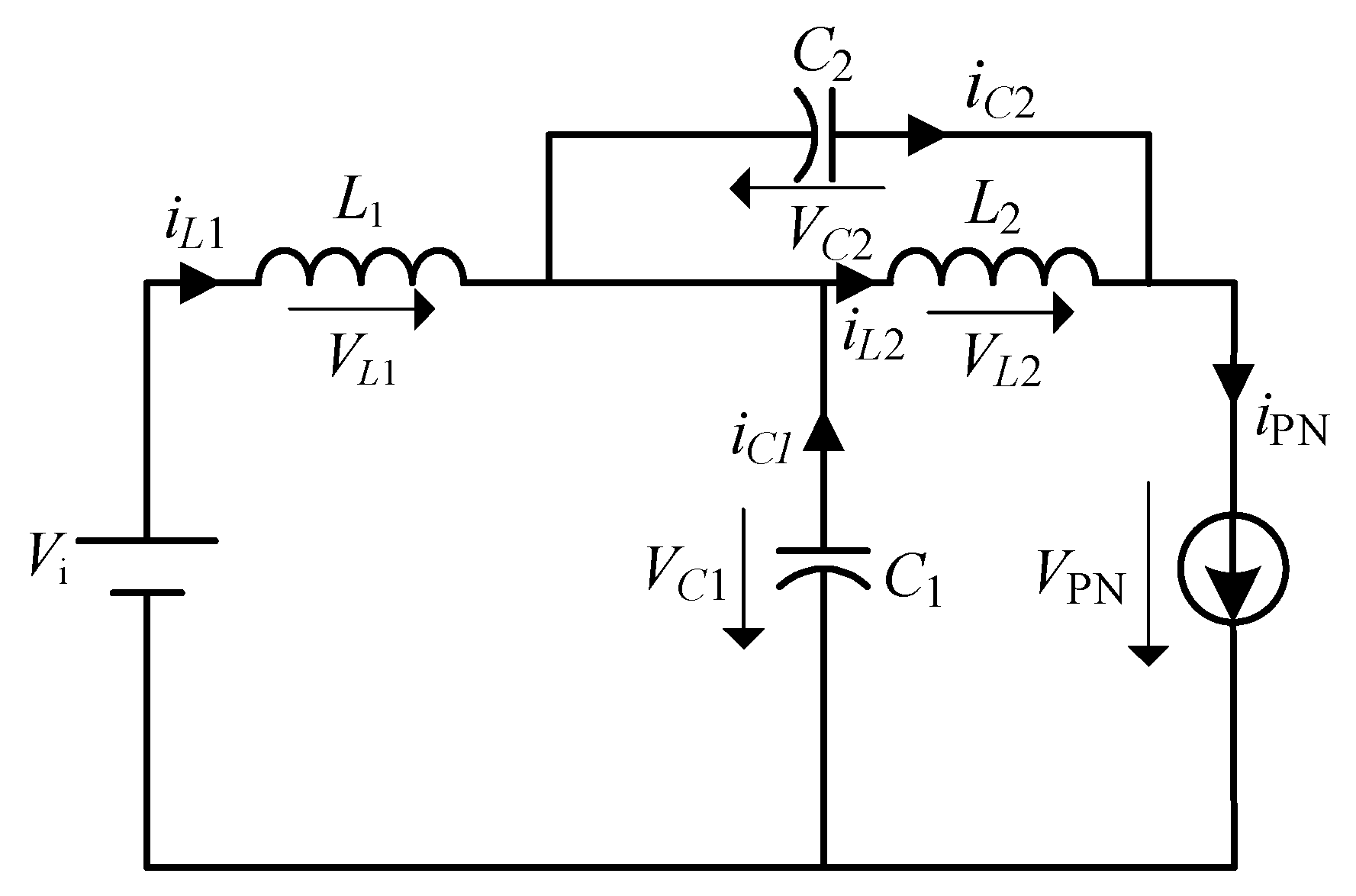
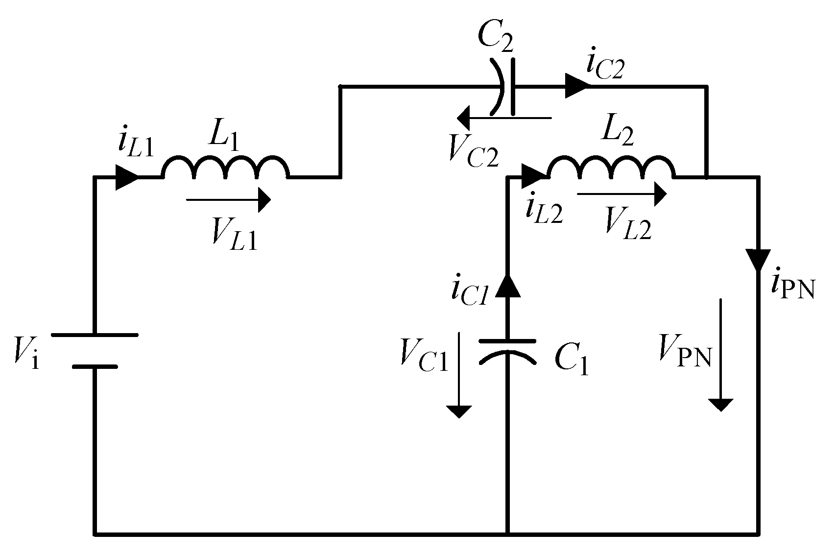
The equivalent circuits for the non-shoot-through state and the shoot-through state are shown in Figure 2 and Figure 3, respectively.
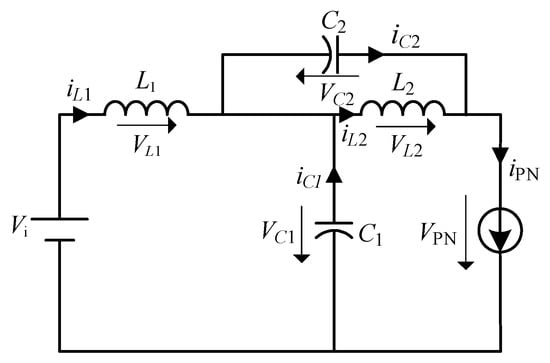
Figure 2.
Equivalent circuit in non-shoot-through state.

Figure 3.
Equivalent circuit in shoot-through state.
As the impedance network is a symmetrical network, C1 = C2 and L1 = L2, which can be obtained as follows:
where VC1 and VC2 represent the voltages across the capacitors C1 and C2, while VL1 and VL2 denote the voltages across inductors L1 and L2, respectively.
In the non-shoot-through state, the inductors L1 and L2 store energy, while capacitors C1 and C2 release energy. Equations (2) and (3) can be obtained using Kirchhoff’s Voltage Law (KVL) and Kirchhoff’s Current Law (KCL):
where Vi represents the DC input current, and VPN represents the DC bus voltage.
where iC1 and iC2 represent the currents flowing through capacitors C1 and C2, respectively. iVD represents the current flowing through diode VD. iL1 and iL2 represent the currents flowing through inductors L1 and L2, respectively. iPN represents the DC bus current.
In the shoot-through state, H-Bridge is short-circuited and the diode VD is in the off state. The inductors L1 and L2 release energy, while the capacitors C1 and C2 store energy. Equations (4) and (5) can be obtained from KVL and KCL:
At steady-state, the voltages across the inductors L1 and L2 are both zero within one cycle. Using Equations (2) and (4) and the volt-second balance, Equation (6) can be obtained:
where and are the average values of the voltage across the inductors over one cycle, T0 is the time in the shoot-through state, T1 is the time in the non-shoot-through state, and the period T = T0 + T1.
At steady state, the capacitor current is zero over one period. Using Equations (3) and (5) and the charge balance, Equation (7) can be obtained:
where and are the average values of the capacitor currents over one period.
Equation (8) can be obtained from Equations (6) and (7),
where D represents the duty cycle of the shoot-through state, while . and are the average values of the inductor currents about L1 and L2.
From Equations (2) and (8), Equation (9) can be obtained:
where B is the boost factor, .
The output voltage and current on the AC side can be written as follows:
where ω is the fundamental angular frequency, φL is the power factor angle, and Vo and Io are the rms output voltage and current, respectively.
The expression of the output instantaneous power on the AC side is
The relationship between the output voltage and the DC bus voltage VPN can be expressed as
From Equations (10) and (12), the peak output voltage of the single-phase inverter is given by
where M is the modulation index, and G is the boost coefficient of the quasi-Z-source inverter.
When the circuit is in the shoot-through state, the DC bus voltage is zero; when the circuit is in the non-shoot-through state, the power is transferred from the DC side to the AC side. If the intermediate losses are neglected, Equation (14) can be written as
The DC bus current expression can be obtained using Equations (12) and (14)
where IPN is the DC component, and is the 2ω component of the DC bus current. The inductor currents iL1 and iL2 and capacitor voltages vC1 and vC2 in the impedance network are directly influenced via iPN, so that
where are the 2ω components of the corresponding currents and voltages, respectively.
When the DC input voltage is constant, the power supply and capacitors charge the inductors in the shoot-through state, and there exists a 2ω component relationship.
In the non-shoot-through state, the power supply and the inductors charge the capacitors with the following 2ω component relationship.
The impedance network is a symmetrical structure, (i.e., L1 = L2 = L, C1 = C2 = C). From Equations (17) and (18), one can write
are in the same phase with , while are at a phase lag of 90 degrees with ; thus, it follows that
where and are the peak values of 2ω ripple in the current of inductor L1 and the voltage of capacitor C1, respectively.
From Equations (19) and (20), the inductance and capacitance 2ω ripple expression in the impedance network can be presented by
The expression for the inductor current and capacitor voltage 2ω ripple of a conventional QZSI impedance network can be found in Equation (21). If the 2ω pulsating power in Equation (21) is made to be zero, and can be realized, which constitutes the active decoupling method for the integrated third bridge leg.
2.2. Circuit Topology of the Proposed Inverter
The circuit topology of the single-phase three-leg QZSI is shown in Figure 4.

Figure 4.
Circuit topology of single-phase three-leg QZSI.
The circuit is designed to be integrated with an additional third bridge leg, which is based on a conventional single-phase QZSI. Through injecting harmonic voltage into the third leg of the bridge, the output 2ω ripple power is reduced to zero (i.e., ), thus reducing the 2ω ripple in the impedance network of inductors and capacitors to a very small value. Notably, the impedance network is still designed with symmetrical parameters, where L1 = L2 and C1 = C2.
2.3. Operating Principle of the Proposed Inverter
The single-phase three-leg QZSI has two operating states: the shoot-through state and the non-shoot-through state. In the non-shoot-through state, the upper and lower switches in the same bridge leg of the inverter conduct in a complementary manner.
Using ST indicates the shoot-through state, while S (SA, SB, SE) indicates the non-shoot-through state, where SA, SB, and SE can take the value of 0 or 1, the value of 0 indicates that the switch below the corresponding bridge leg is turned on, and the value of 1 indicates that the switch above the corresponding bridge leg is turned on. The topology operating states and points A, B, and E voltage are shown in Table 1.

Table 1.
Operating states and voltage at points A, B and E.
Based on Table 1, it can be observed that the voltages at points A, B, and E, which are denoted as vA, vB, and vE, respectively, only have two possible values: VPN and 0. Using the Fourier transform, vA, vB, and vE can be expressed as follows
where VdcA represents the DC component of the voltage at point A, while An represents the amplitude of the nth harmonic component of the voltage at point A. VdcB represents the DC component of the voltage at point B, and Bn represents the amplitude of the nth harmonic component of the voltage at point B. Vdc2 represents the DC component of the voltage at point E, and Vn represents the amplitude of the nth harmonic component of the voltage at point E.
The expression of the fundamental frequency component of the output voltage is shown in Equation (10), and if the filter inductor voltage drop values are neglected, the following can be obtained
The following Equation (24) is given by Equations (10), (22), and (23).
It can be seen that the addition of the third bridge leg does not affect the inverter output. To simplify the analysis, the following relationship is taken.
Vdc1 represents the DC component of the voltage at point A and point B.
The output filter capacitor voltage and inductor current can be written as follows
where vo1 and vo2 represent the voltages across the output filter capacitors Cf1 and Cf2, respectively, while io1 and io2 represent the currents through the output filter inductors Lf1 and Lf2, respectively. Cf denotes the output filter capacitor, Cf1 = Cf2 = Cf, Vdc = Vdc2 − Vdc1, and
The instantaneous power of the output filter capacitor is given by
Substituting A1 + B2 = 0 into Equations (24) and (27), the following results can be obtained
Using buffer , such that . To eliminate , only the second harmonic is retained in QE; therefore, QE can be expressed as follows
Equation (31) can be obtained from the above analysis
Using the 2ω pulsating power to offset , the amplitude and phase of the injected second harmonic voltage can be obtained
Although the 2ω pulsating power is buffered when injecting the second harmonic voltage in the third bridge leg, a new 4ω pulsating power is generated. If the third bridge leg simultaneously injects a fourth harmonic voltage, the following results can be obtained
Through setting in Equation (33), Equation (34) can be obtained as follows
Based on Equation (34), the amplitude and phase of the injected fourth harmonic voltage can be obtained as follows
It can be observed that injecting low-frequency harmonic voltages into the third bridge leg can eliminate the ripple power at the pre-determined frequency; however, at the same time, new frequency-dependent ripple power is generated. If a third harmonic voltage is injected simultaneously, the following results can be obtained
It can be deduced from Equation (36) that, in this case, the ripple power at 6th harmonic frequency can be eliminated; however, at the same time, new ripple powers at the first, second, third, fifth, seventh, and eighth harmonic are generated.
Table 2 presents the correlation between the input current harmonic content and the frequency of the injected harmonic voltage in the additional bridge leg, with parameters set to f = 50 Hz, P = 300 W, Vi = 144 V, Vdc = 150 V, Cf = 52 μf, Vo = 110 V, and φL = 0. Analysis of Table 2 indicates that the harmonic content of the input current is relatively insignificant in comparison to the DC component when the additional bridge leg injects second and fourth harmonic voltages simultaneously. However, injecting second, third, and fourth harmonic voltages actually increases the ripple content of the input current. These observations reveal that injecting specific combinations of harmonic voltages can impact the harmonic content of the input current, highlighting the importance of carefully selecting the appropriate harmonic injection strategy to minimize undesirable effects on the system.

Table 2.
Relationship between input current harmonic content and injected harmonic voltages.
The expressions for the voltages at points A, B, and E when the additional bridge leg injects second-frequency and fourth-frequency harmonic voltages are as follows
The following relationships need to be satisfied for the shoot-through modulation signals Vcom1 and Vcom2.
Based on the above equation, when vA, vB, and vE satisfy Equations (37) and (38), the inverter can simultaneously achieve boosting, inversion, and low-frequency ripple suppression of input current.
3. The Control Strategy of the Proposed Inverter
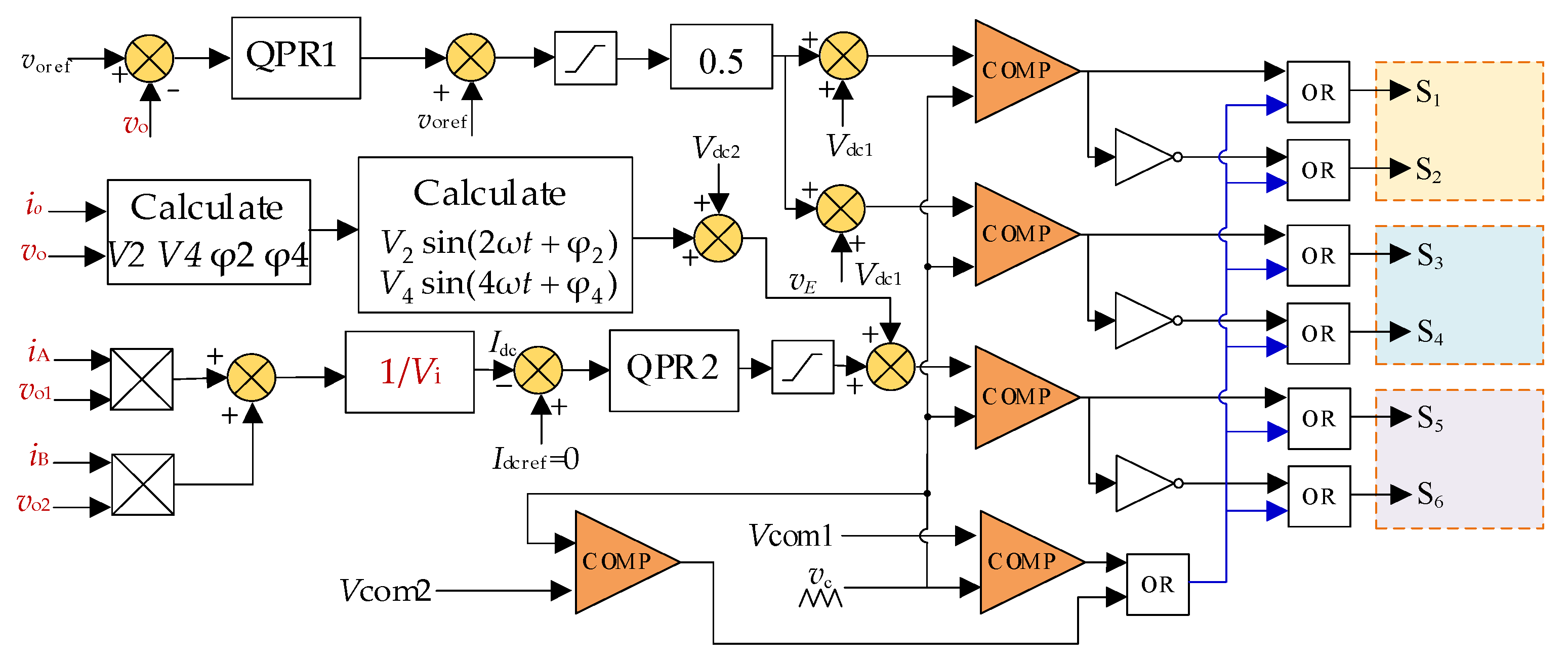
Figure 5 illustrates the control strategy employed for the single-phase three-bridge-leg of QSZI. The shoot-through state modulation is achieved using open-loop simple boost control, while constant output voltage control is employed for the two bridge-leg of H-Bridge. For the additional third bridge-leg, a control method is employed that injects specific frequency harmonic voltage and suppresses newly generated low-frequency components of the input current. The controllers utilize a quasi-PR (QPR) control strategy. The transfer function of the QPR control incorporates the transfer function of the sinusoidal signal, which is represented as ω/s2 + ω2. This process enables accurate tracking of the sinusoidal signal without any static errors.

Figure 5.
Control strategy of proposed inverter.
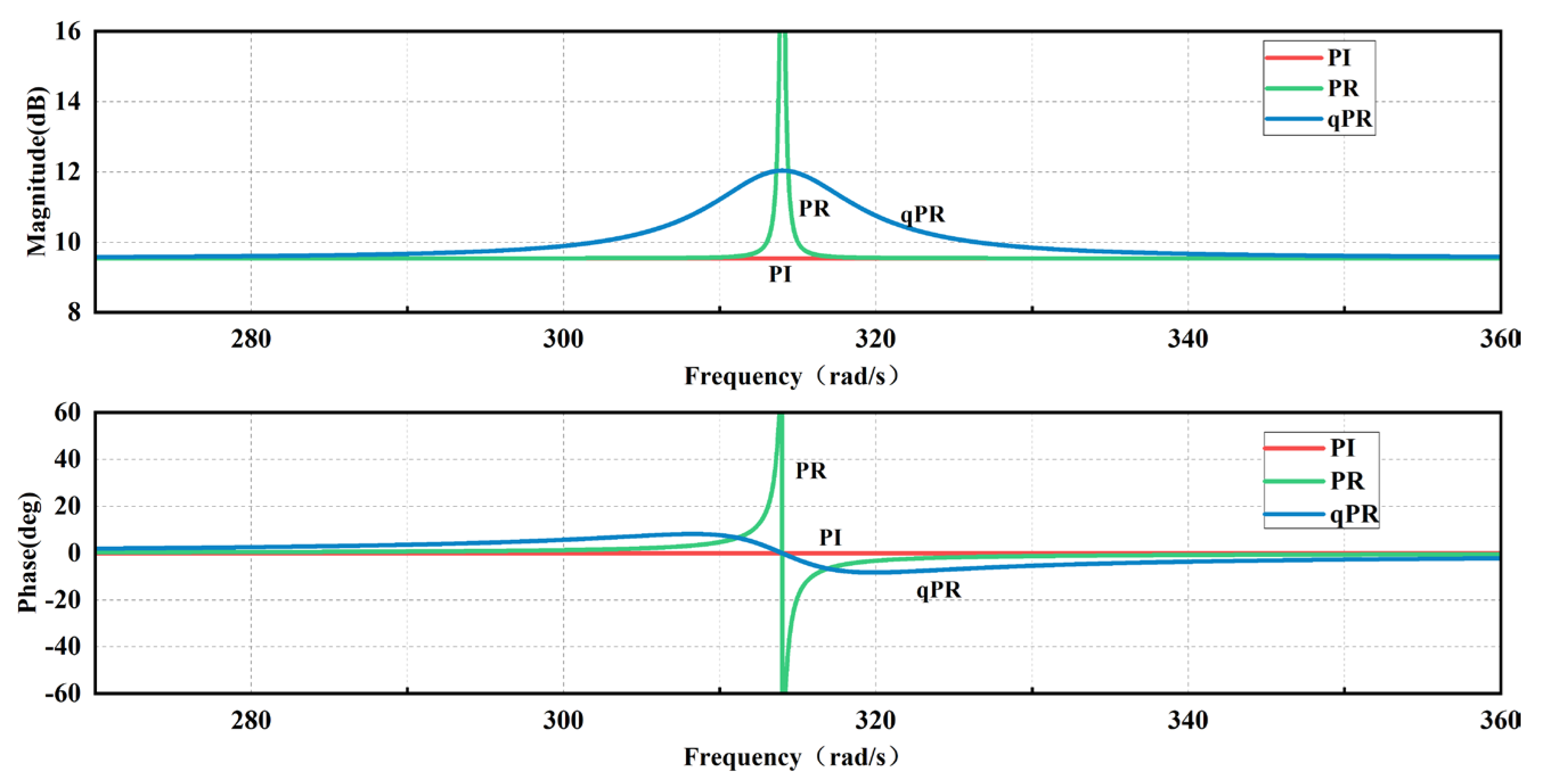
Figure 6 illustrates a comparison of the Bode diagrams for the PI, PR, and QPR controllers. It is evident that the QPR controller exhibits superior bandwidth and enhanced stability, even in the presence of output target frequency perturbations, as compared to the PI and PR controller.
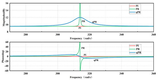
Figure 6.
Comparison of PI, PR, and QPR Bode diagrams.
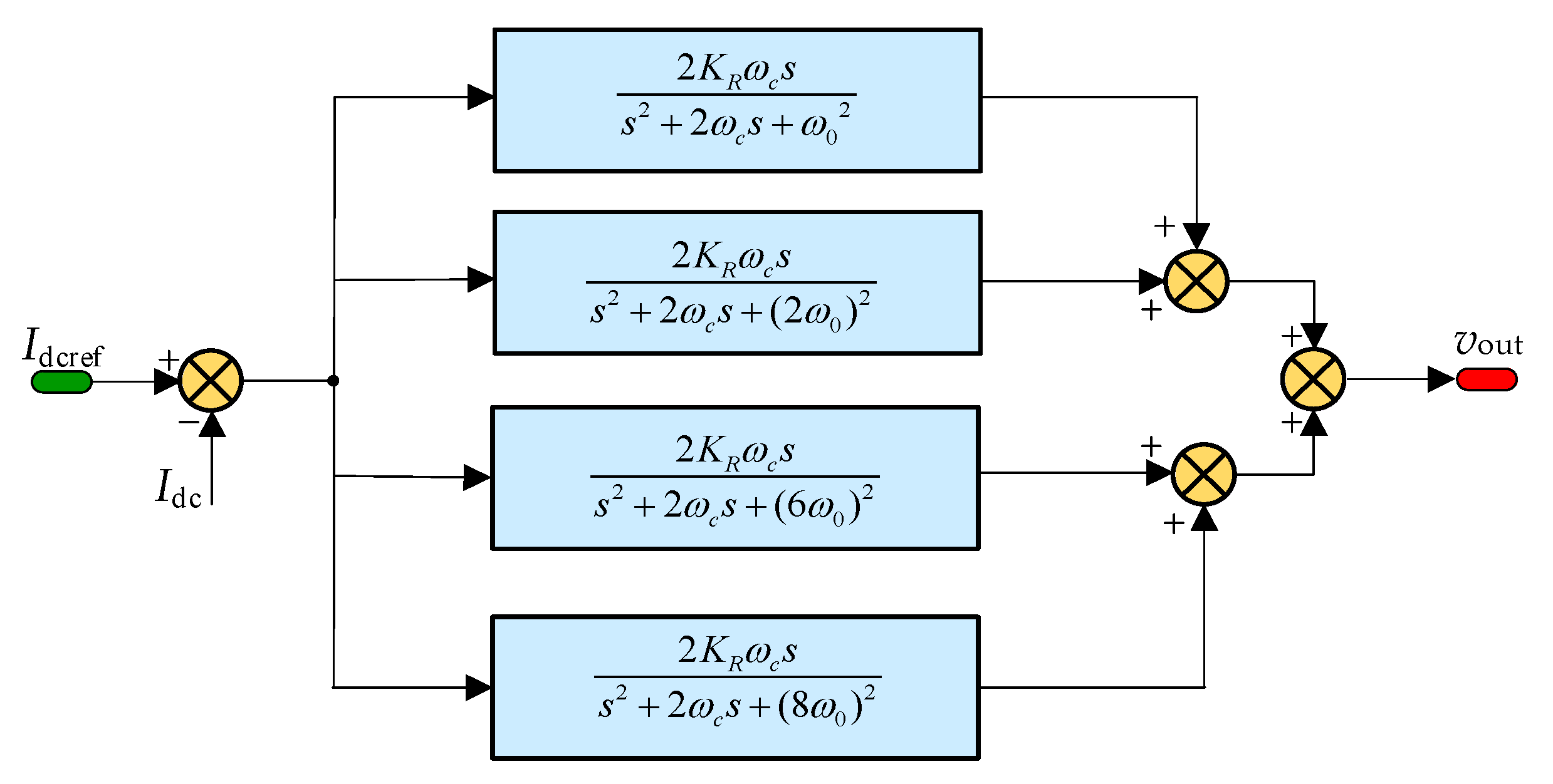
The amplitude–frequency characteristics of the QPR controller clearly indicate that the gain approaches zero at frequencies other than the resonant frequency point. This characteristic empowers the QPR controller with the ability to effectively suppress harmonics at specific frequencies. Figure 7 presents the structural diagram of QPR2, which is designed based on this principle.
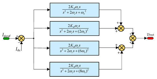
Figure 7.
Structure of QPR2.
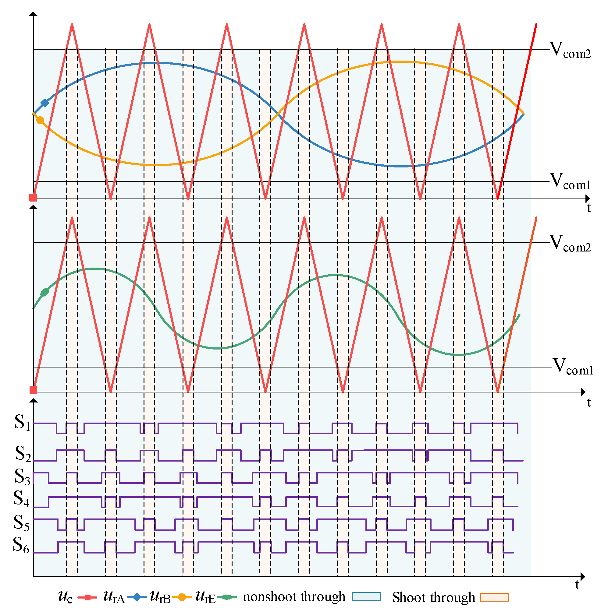
The modulation waveforms of the system are shown in Figure 8, where the A and B bridge legs, as well as the E bridge leg, adopt independent simple Sinusoidal Pulse Width Modulation (SPWM) strategies. The modulation waveforms of the three bridge legs are represented by urA, urB, and urE, with a triangular waveform uc as the carrier signal. When ur ≥ uc, the switches of the upper leg of the corresponding bridge leg are turned on, while the switches of the lower leg are turned off. When ur ≤ uc, the switches of the upper leg of the corresponding bridge leg are turned off, and the switches of the lower leg are turned on. When uc ≥ Vcom1 or uc ≤ Vcom2, the bridge leg is in a shoot-through state.
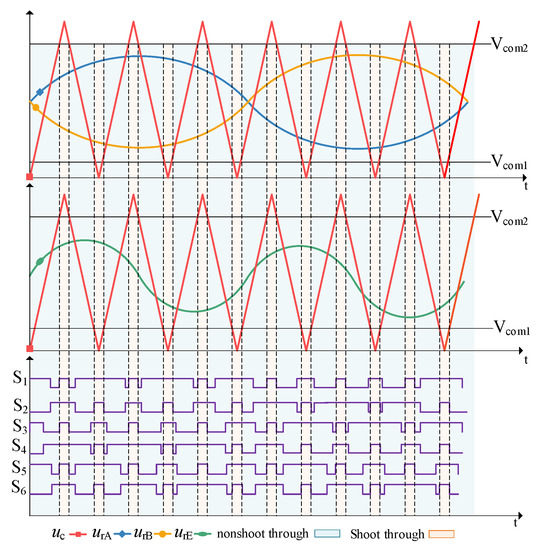
Figure 8.
Modulation waveform of system.
4. Parameter Design of the System
4.1. Parameter Design of Inductance and Capacitance in Impedance Network
The implementation of the active filtering technique effectively minimizes ripple power in the output power, resulting in the complete suppression of 2ω ripple on the DC side. Therefore, the inductors and capacitors in the impedance network do not need to buffer the 2ω ripple according to Equation (21), but only need to suppress the switching frequency ripple. When the inductances L1 and L2, as well as the capacitance C1 and C2 in the impedance network, satisfy the following relationship, they can suppress the switching frequency current ripple and voltage ripple, respectively.
where W1 denotes the percentage of current ripple at the frequency of the inductive switch, W2 represents the percentage of voltage ripple at the frequency of the capacitive switch, W1 is usually selected as 20%, and W2 is selected as 1%. D denotes the duty cycle of the shoot-through, and fs represents the switching frequency.
4.2. Parameter Design for Modulation of the Third Bridge Leg
The selection of parameters Vdc and Cf in Equation (32) is directly correlated with crucial circuit parameters, such as the input voltage level and the voltage stress on switches, which impact the overall performance of the circuit. Therefore, a more comprehensive and in-depth analysis is required to thoroughly understand the interdependence of these parameters.
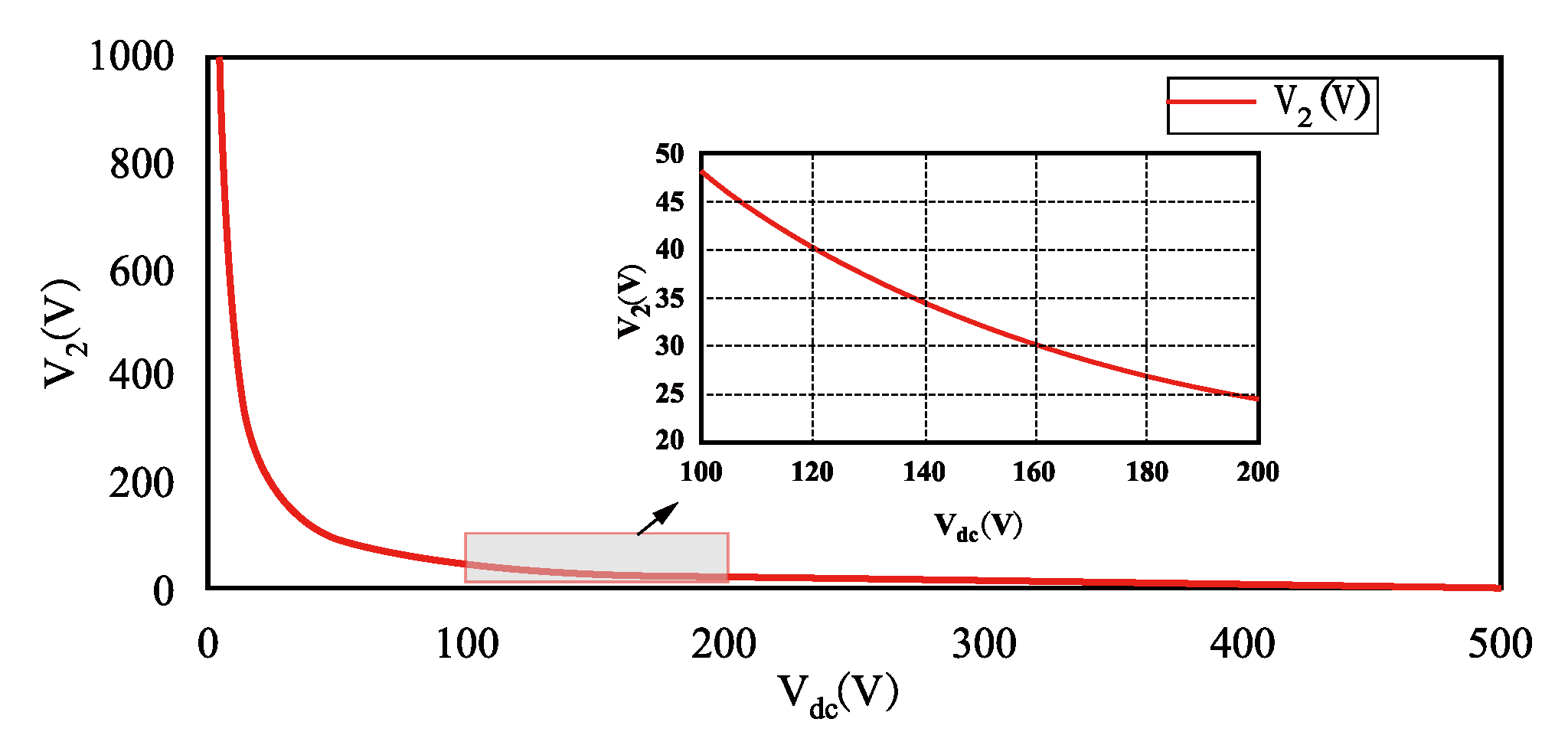
Based on Equation (33), the relationship between the values of the DC bias voltages Vdc and V2 can be obtained when S = 300 VA, Cf = 52 μf, and φL= 0, as shown in Figure 9. From Figure 9, it can be inferred that the value of V2 decreases as the value of Vdc increases. Hence, it is crucial to avoid selecting an excessively small value for Vdc to prevent V2 from becoming excessively large. Furthermore, the values of Vdc and V2 are closely related to the magnitude of VPN; the DC bus voltage, which is dependent on the input voltage; and the shoot-through duty cycle. As a result, the value of Vdc should also not be excessively large.
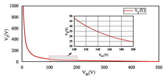
Figure 9.
Relationship between Vdc and V2.
Based on the analysis, it is concluded that selecting Vdc within the range of 100 V to 200 V is more reasonable. The minimum value of VPN is related to other parameters, as shown in Table 3. It is worth noting that VPNmin remains constant for both schemes. According to Equation (31), when the second harmonic power in the output power is cancelled out due to the second harmonic power in the p2cf, Equation (40) can be obtained.

Table 3.
Relationship between VPNmin and other parameters in two schemes.
Through analysis, when Vdc1 is greater than Vdc2, the following situations occur:
When φV2 is located in the second quadrant. When φV2 is located in the third quadrant.
When Vdc1 is less than Vdc2, φV2 is always located in the first or fourth quadrant. Therefore, it can be seen that selecting the second scheme where Vdc1 ≤ Vdc2 is more in line with the actual situation and easier to implement. Therefore, Vdc1 is chosen to be less than or equal to Vdc2, and the value of Vdc is set to 150 V.
In comparison to the conventional two-leg inverter, the three-leg inverter topology necessitates a higher DC bias value, resulting in a corresponding requirement for a higher DC bus voltage. As shown in Equations (37) and (38), the DC bus voltage needs to satisfy the following expression
Since Vdc1 ≤ Vdc2, Vdc = 150 V is chosen, and one can simply write
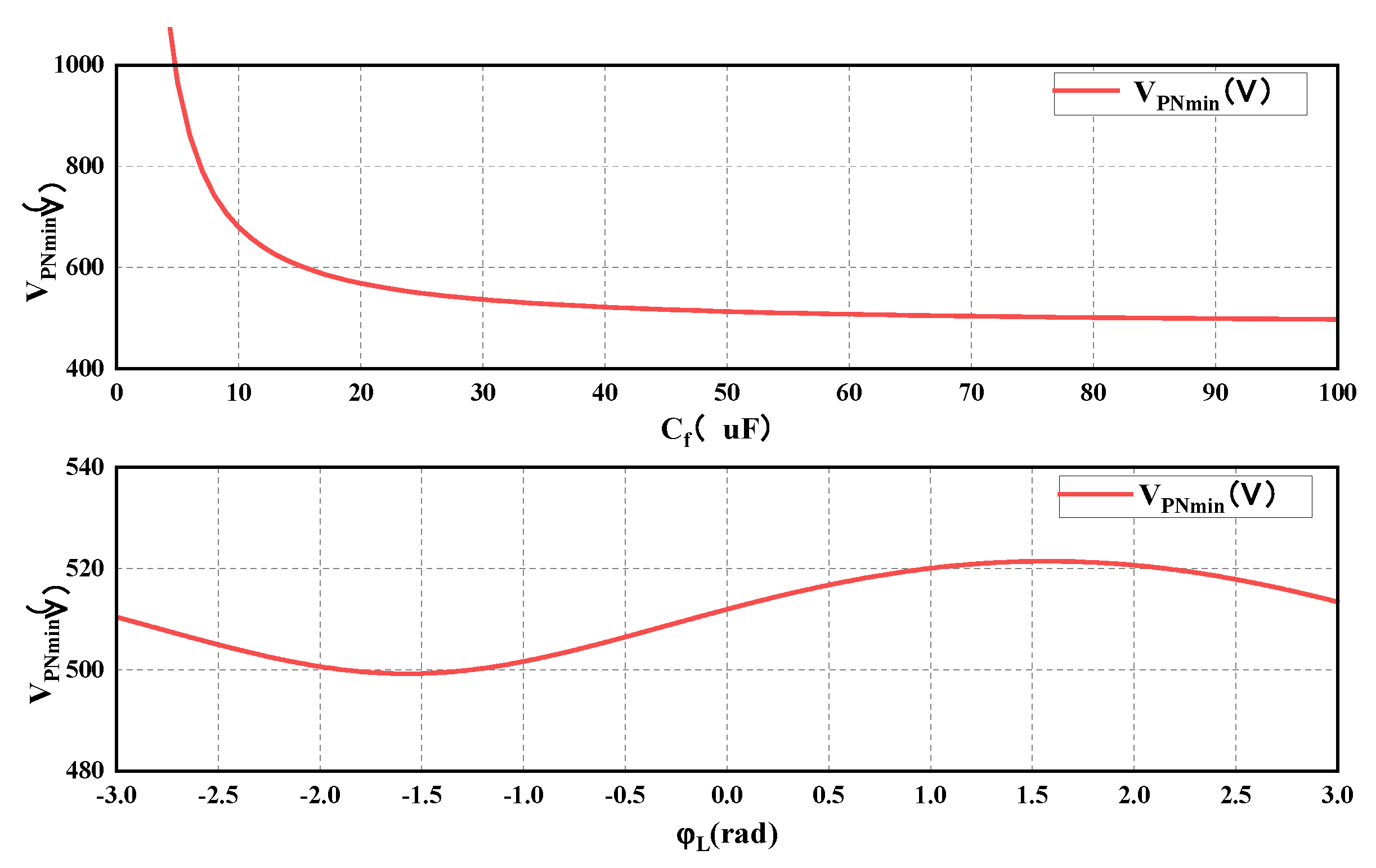
The correlation between the minimum DC bus voltage, VPNmin, and capacitance, Cf, is presented in Figure 10 for the specific case of S = 300 VA, Vdc = 150 V, and φL = 0. Furthermore, Figure 10 depicts the relationship between VPNmin and the power factor angle, φL, in the case of S = 300 VA, Cf = 52 uF, and Vdc = 150 V.
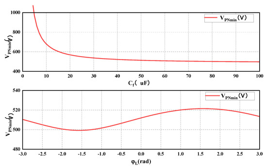
Figure 10.
Relationship between VPNmin and Cf, φL.
The selection of the injected secondary harmonic voltage V2 should be 20 to 30% of Vdc when Vdc is chosen as 150 V. Otherwise, it will affect the boosting capability of the quasi-Z-source inverter, thus affecting the value of the DC bus voltage. From Equation (42), the relationship between the injected secondary voltage amplitude V2 and the filter capacitor Cf can be obtained. Based on the range of values for the injected secondary voltage amplitude, the range of Cf can be determined to be 36 to 56 μF.
The results of this investigation highlight that the selection of capacitance Cf is intimately tied to both the voltage stress experienced by the switches and the overall capacity of the system. Hence, a comprehensive evaluation of these factors is crucial in determining the optimal value for capacitance Cf. If the capacitance is too large, it will significantly increase the size of the inverter and the current flowing through the capacitor, which reduces the power density of the inverter and increases the current stress on the power switching devices. Similarly, if the capacitance is too small, the demand for the minimum DC bus voltage is too high, and the voltage stress on the power switching devices increases, which limits the selection of the switching devices.
Taking into account the above analysis, a relatively appropriate range of values can be obtained, and selecting values within this range is acceptable. Finally, a capacitance value of 52 μF was selected.
5. Simulation Results
This section presents the simulation results of the proposed converter and verifies the superiority of the proposed scheme through comparing it with the conventional single-phase QZSI through simulation. A simulation model of the three-bridge-leg QZSI with input ripple suppression is developed using PSIM software (Professional Version 2022.2.0.17), and the system parameters are shown in Table 4.

Table 4.
System parameters.
5.1. Simulation of the System under Full Load
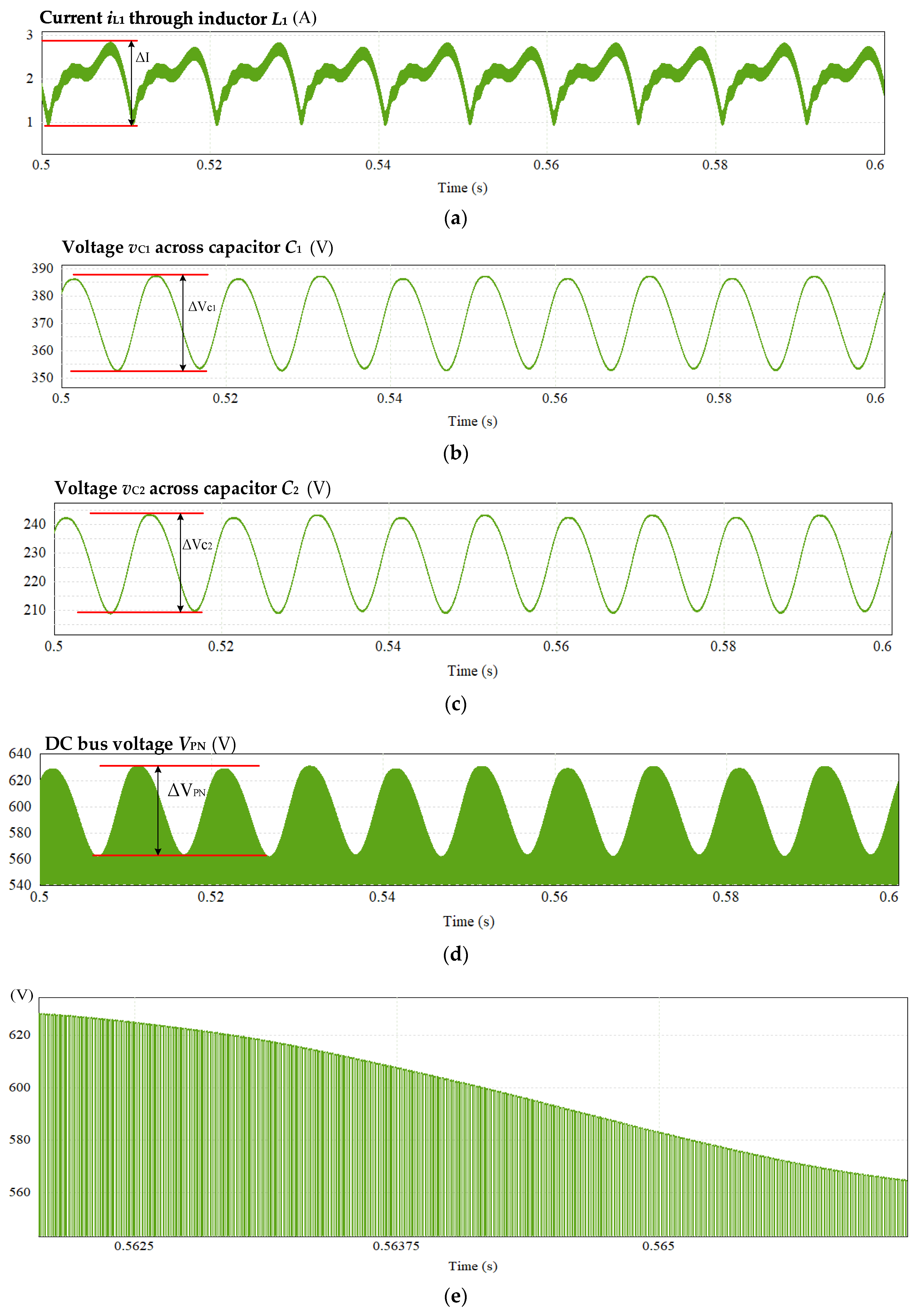
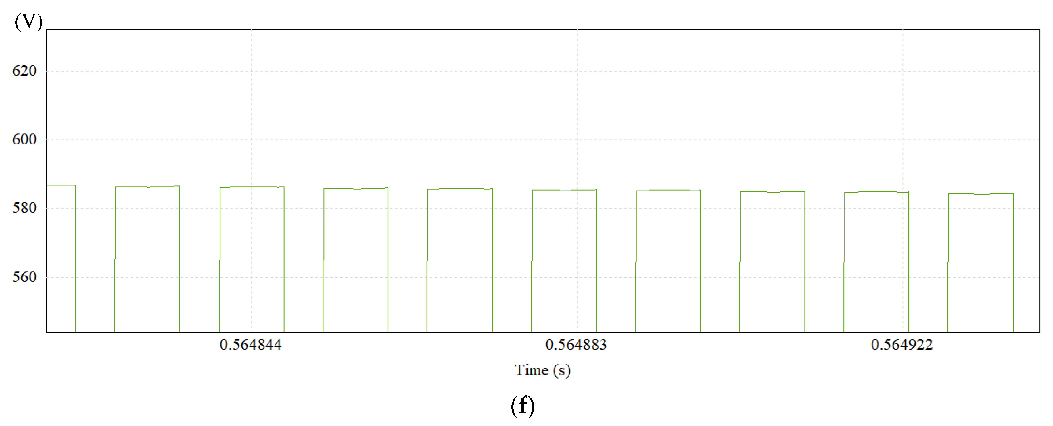
Figure 11 shows the waveform of circuit simulation under full load (300 W) condition with the third leg disabled, using only the passive filtering technique. The average DC-side current is theoretically calculated as 2.08 A; the voltages across capacitor C1 and C2 are 360 V and 216 V, respectively; and the DC bus voltage VPN is 576 V. According to Figure 11a, it can be observed that the inductor current ripple ΔI is 1.89 A, which is 90.87% of the theoretical value. Figure 11b,c show the voltage ripples across capacitor C1 and C2 are 34.74 V and 35.57 V, respectively. Figure 11d shows the DC bus voltage ripple ΔVPN is 70.75 V, which accounts for 12.28% of the theoretical value. Figure 11e is an enlarged view of the DC bus voltage VPN, and Figure 11f is a further enlarged view of Figure 11e. When VPN is 0, it is in a shoot-through state, and the shoot-through state duty cycle can be calculated as 0.376 from Figure 11f, which is consistent with the set value.
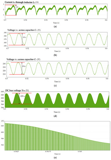
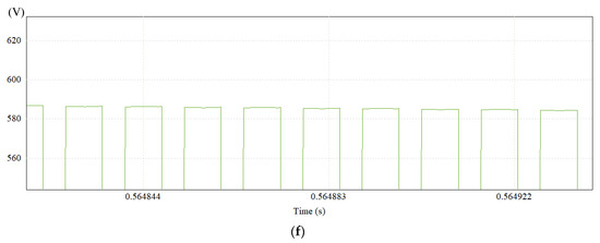
Figure 11.
Simulation waveform of disabling third leg: (a) current of inductor L1, (b) voltage across capacitors C1, (c) voltage across capacitors C2, (d) voltage of DC bus, (e) amplified part of DC bus voltage VPN, and (f) further enlarged view of (e).
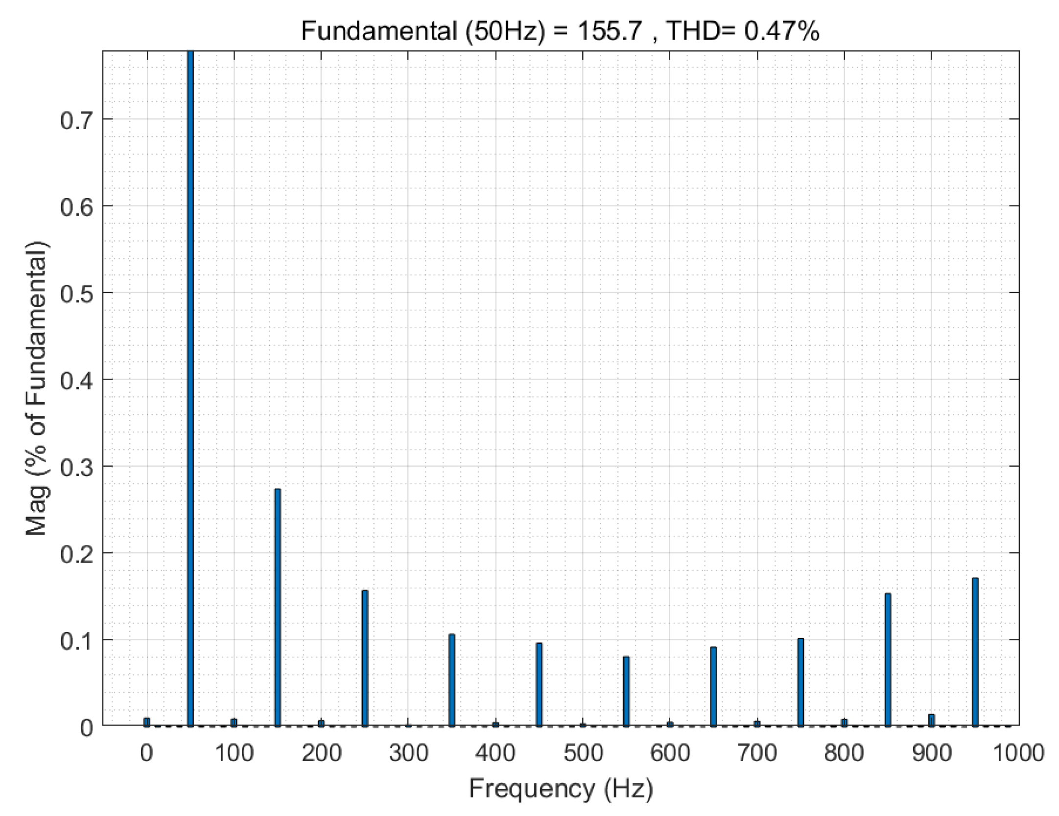
The Fast Fourier Transform (FFT) of the output voltage in this case is shown in Figure 12, with a Total Harmonic Distortion (THD) of 0.47%.

Figure 12.
Fast Fourier Transform (FFT) analysis of output voltage when third bridge leg is disabled.
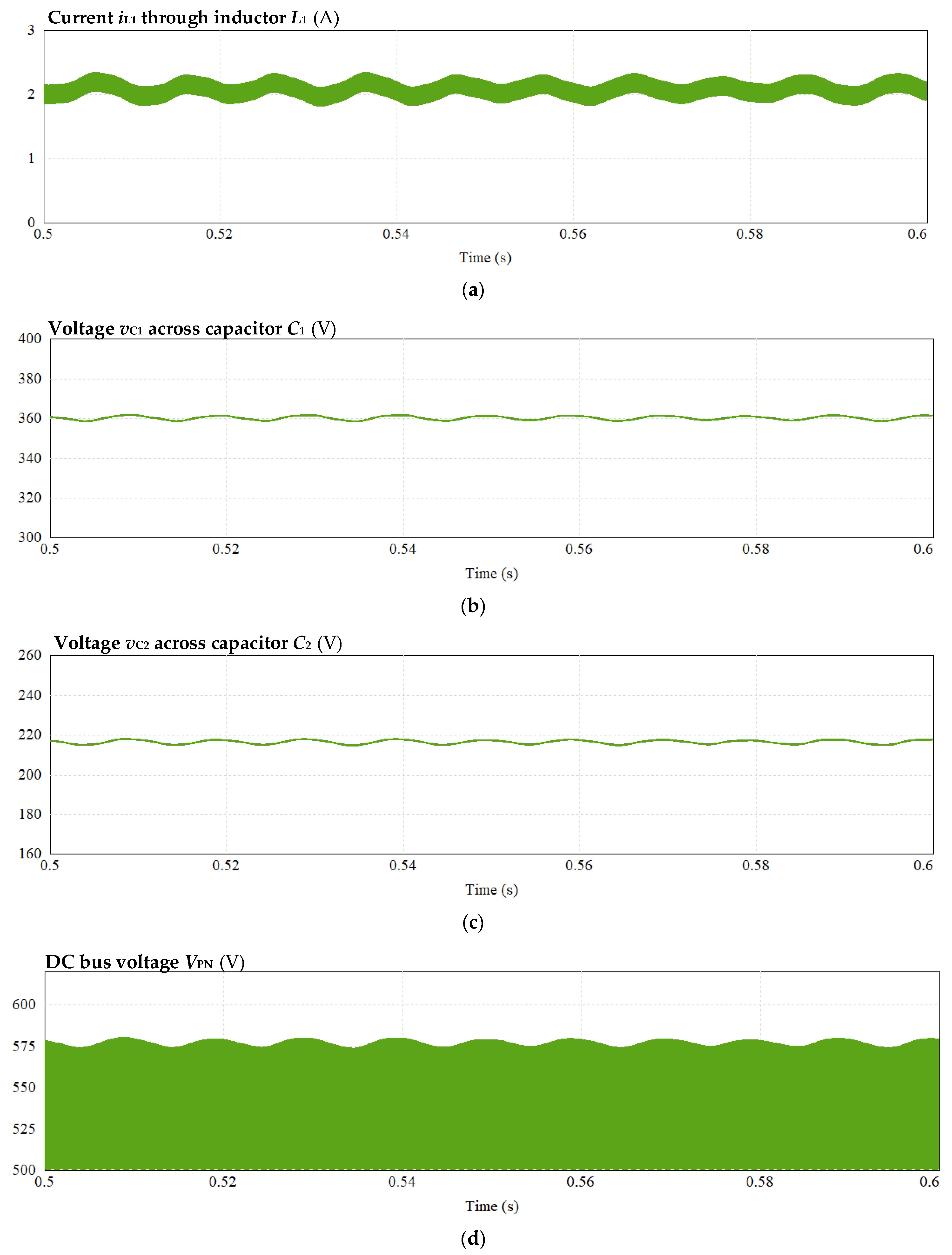
With the third leg enabled, the waveforms of the circuit are shown in Figure 13. Figure 11a shows that the current ripple ΔI of the inductor L1 is 0.513 A, and Figure 13b,c show the ripples of the voltage across capacitors C1 and C2 ΔV are 3.3 V and 3.4 V respectively, accounting for only 0.92% and 1.57% of their theoretical values. Figure 13d shows that the ripple of the DC bus voltage ΔVPN is 6.54 V, which is only 1.14% of its theoretical value.
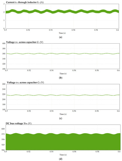
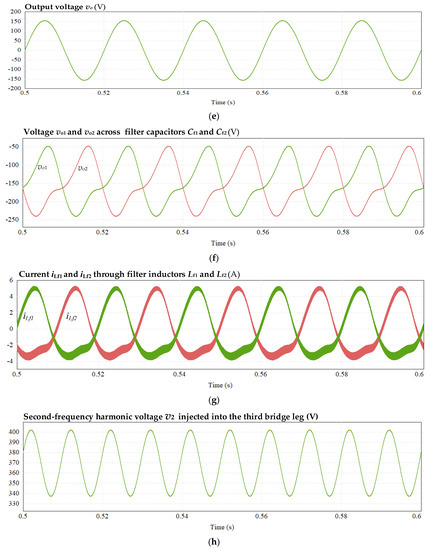

Figure 13.
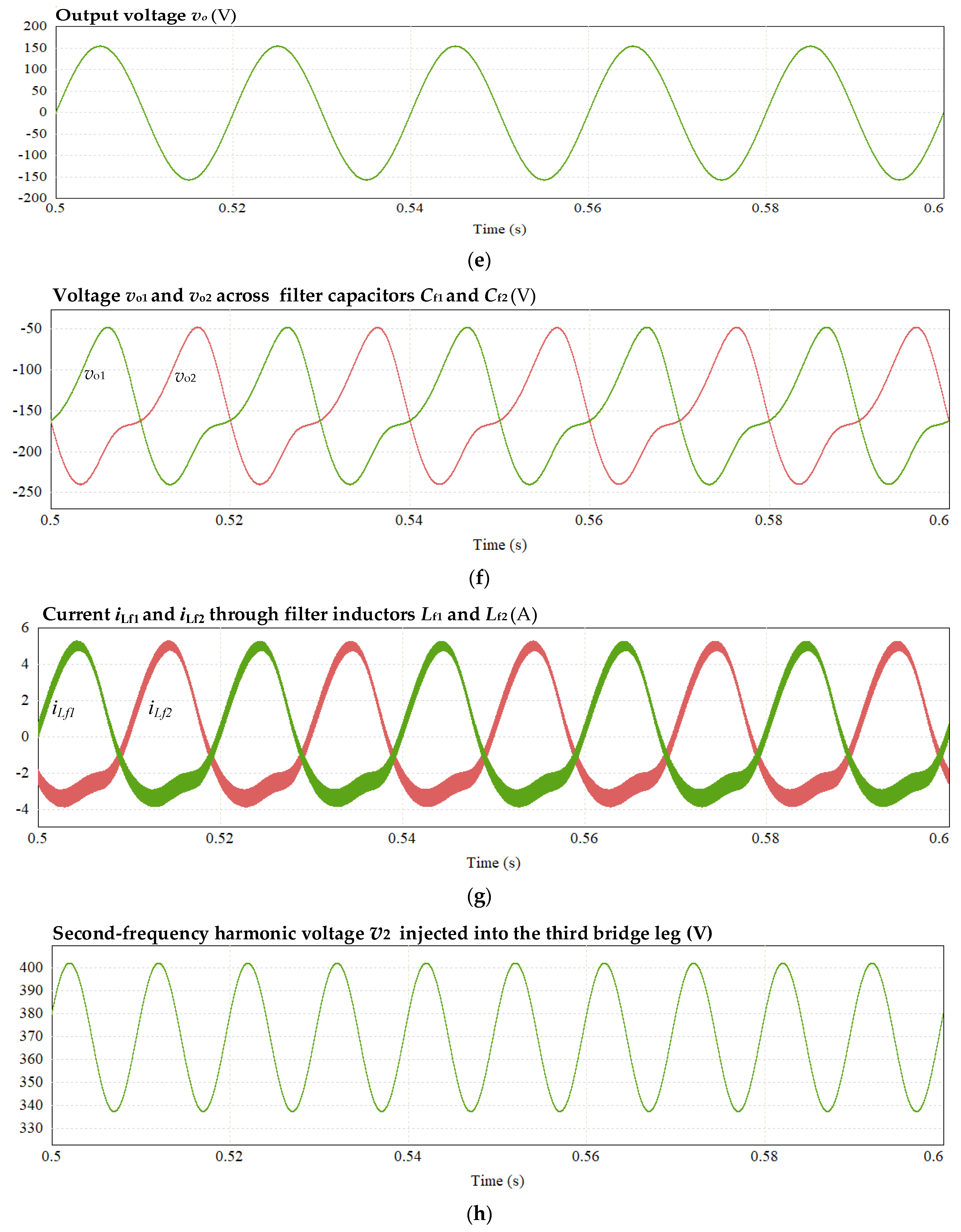
Simulation waveform with third leg enabled: (a) current of inductor L1, (b) voltage across capacitors C1, (c) voltage across capacitors C2, (d) voltage of DC bus, (e) output voltage, (f) voltage across capacitors Cf1 and Cf2, (g) current of inductor Lf1 and Lf2, (h) second-frequency harmonic voltage injected into third bridge leg, and (i) fourth-frequency harmonic voltage injected into third bridge leg.
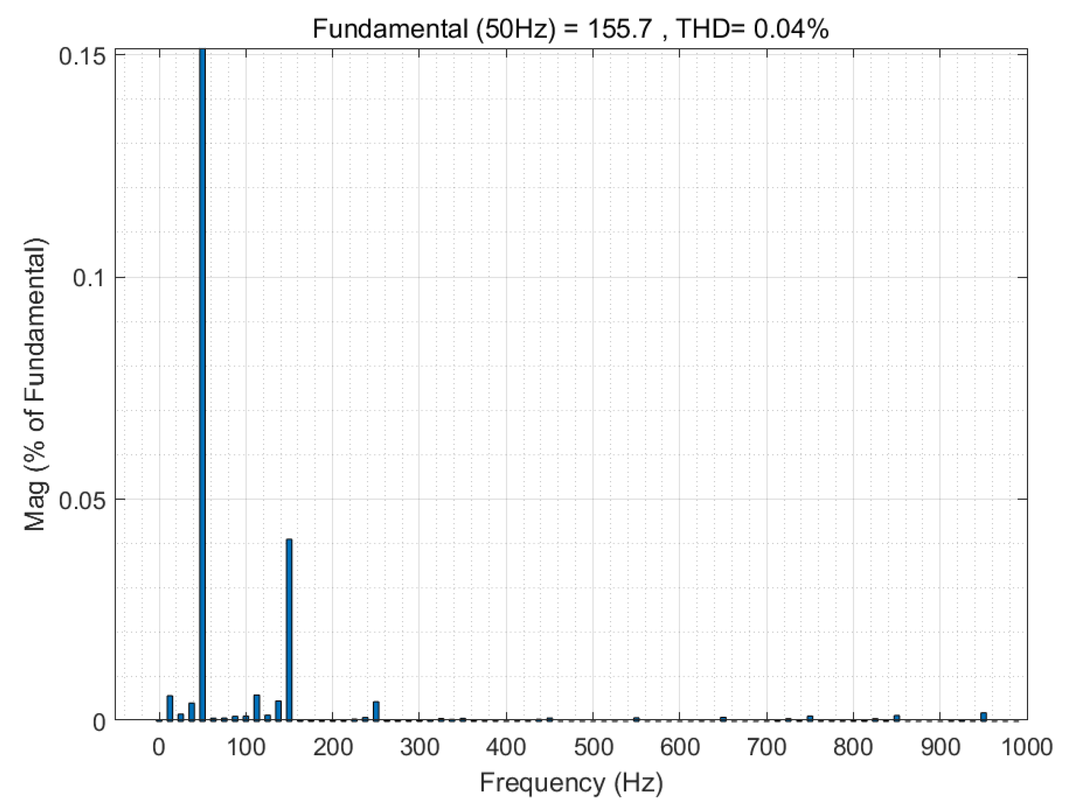
The FFT analysis of the output voltage is shown in Figure 14, and the total harmonic distortion (THD) of the output voltage is only 0.04%, thus being reduced to a value close to zero. It can be seen that the engagement of the third bridge leg did not affect the output performance of the inverter.

Figure 14.
FFT analysis of output voltage when third bridge leg is enabled.
Figure 15 shows the comparison of low-frequency current ripple in the input current before and after enabling the third bridge leg under full load conditions. It can be seen that the low-frequency current ripple in the input current is significantly reduced after enabling the third bridge leg. Specifically, the second harmonic ripple is reduced from 18.2% to 4.5%, and the fourth harmonic ripple is reduced from 16.5% to 2.1%.

Figure 15.
Comparison of low-frequency current ripple in input current before and after enabling third bridge leg under full load conditions.
5.2. Simulation of the System under Underload
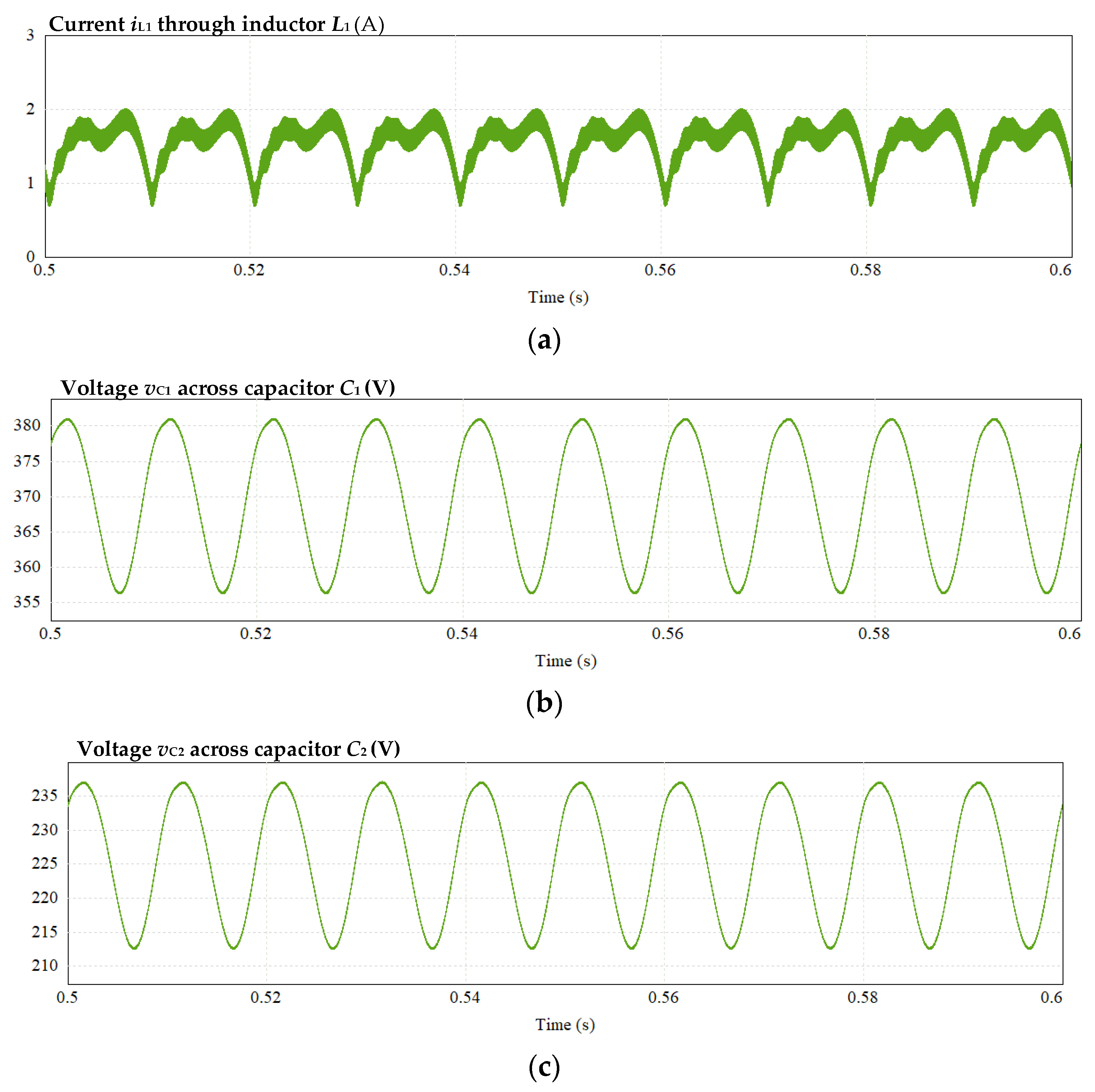
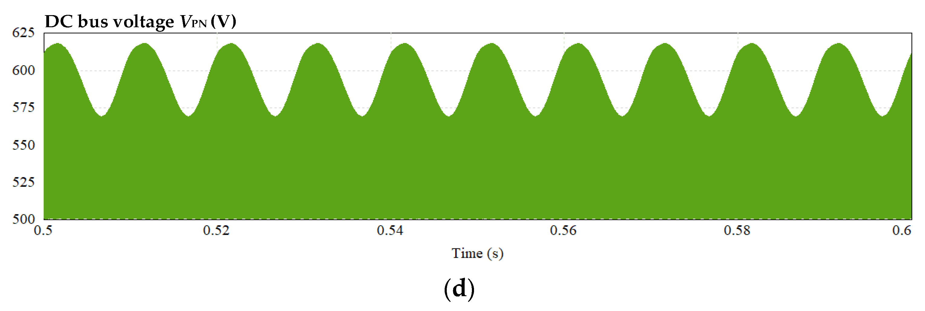
Under the underload (225 W) condition, Figure 16 illustrates the circuit simulation waveform when the third bridge leg is disabled. It can be observed that the inductor current iL1, voltage across capacitors vC1 and vC2, and DC bus voltage VPN contain a high level of low frequency ripple, which can cause distortions in the inverter output voltage and current waveforms, leading to a shorter system lifespan.
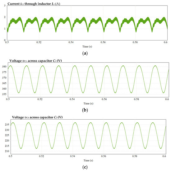
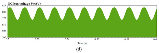
Figure 16.
Simulation waveform of disabling third leg: (a) current of inductor L1, (b) voltage across capacitors C1, (c) voltage across capacitors C2, and (d) voltage of DC bus.
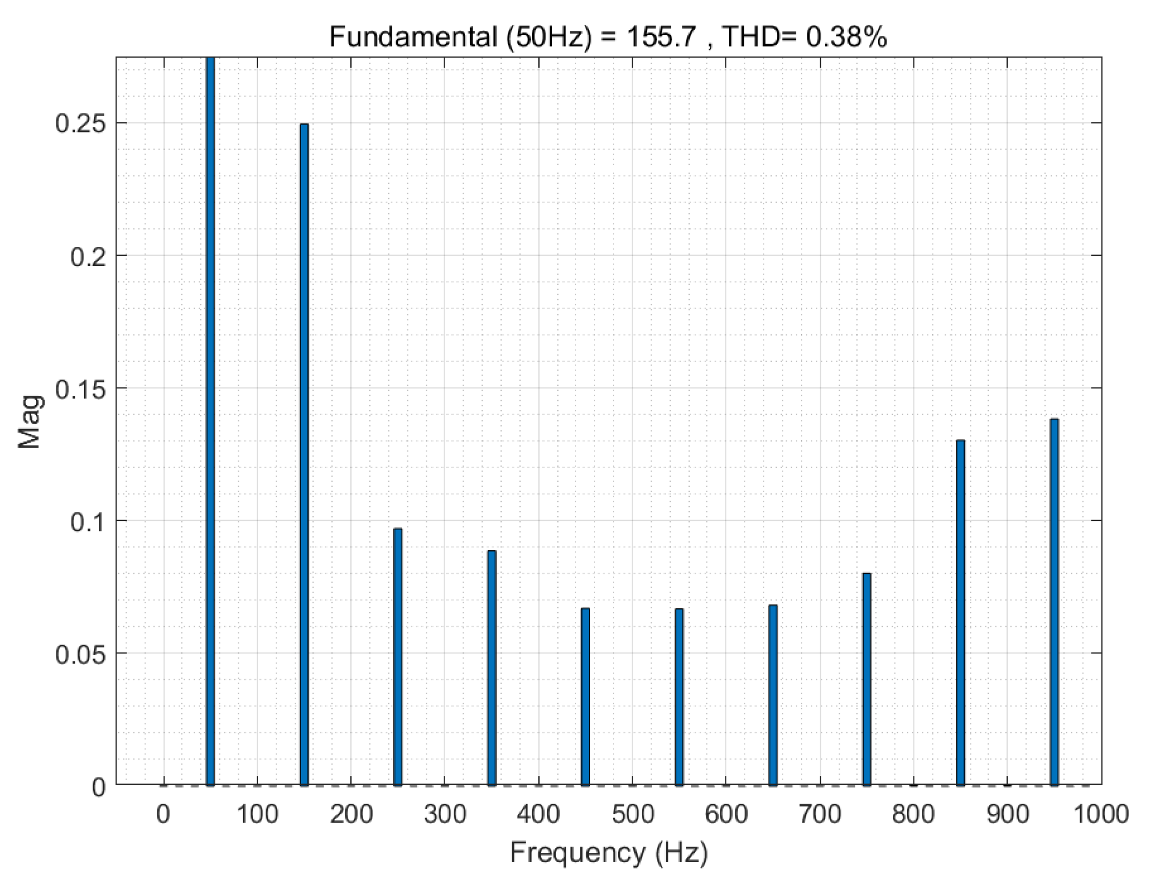
The FFT of the output voltage in this case is shown in Figure 17, with a THD of 0.38%.
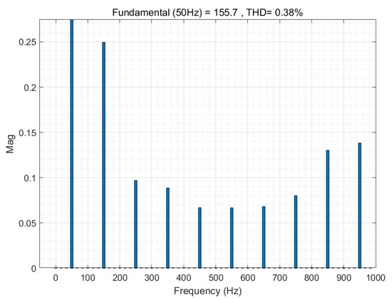
Figure 17.
FFT analysis of output voltage when third bridge leg is disabled.
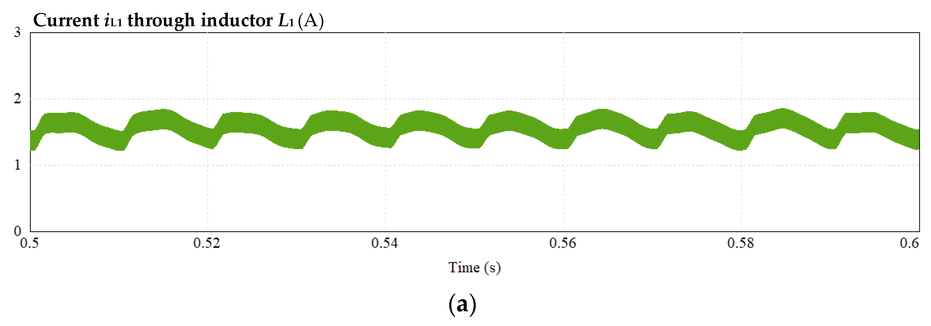
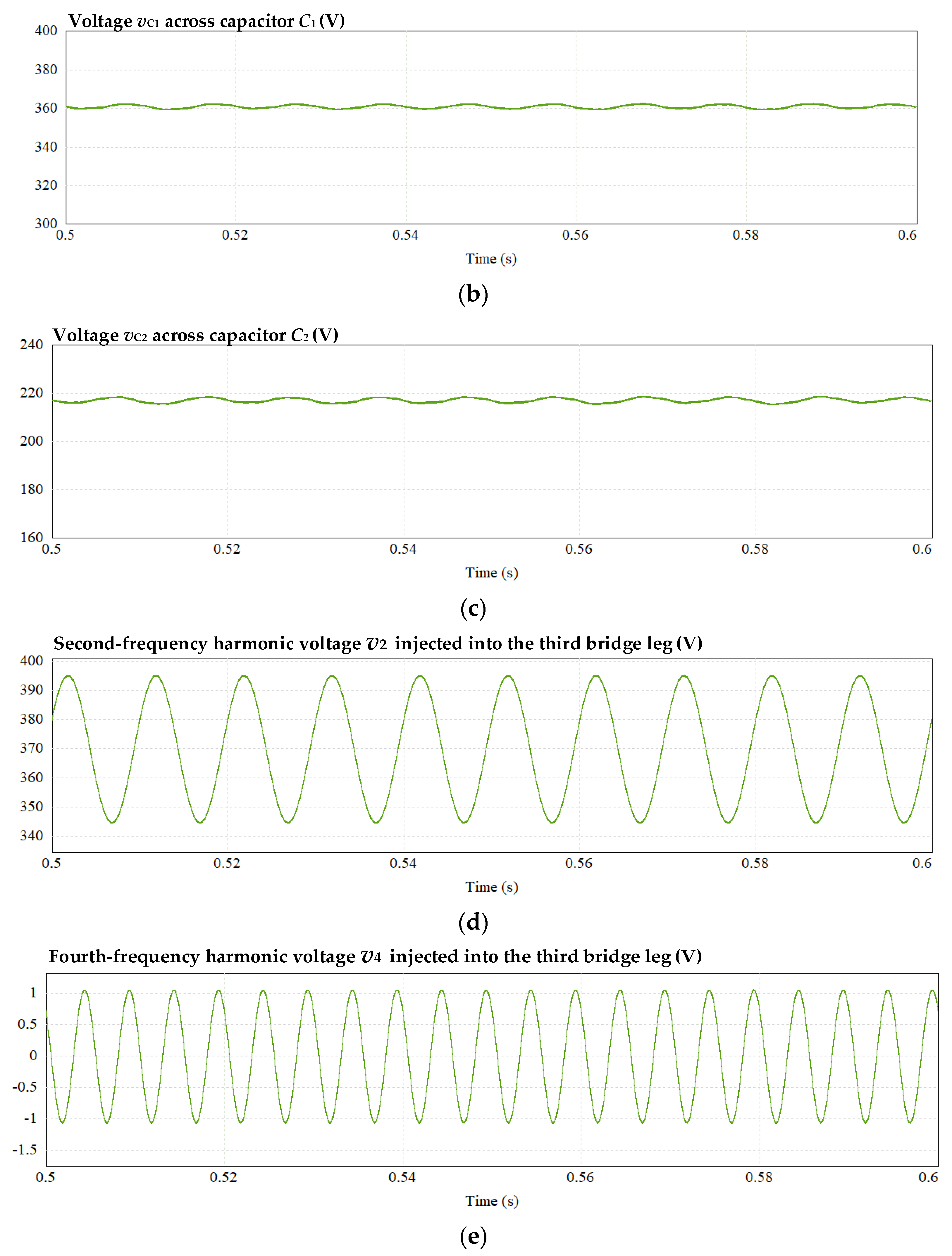
With the third leg enabled, the waveforms of the circuit are shown in Figure 18. From Figure 18a–c, it can be observed that the inductor current iL1, capacitor voltages vC1, and vC2 contain only a small amount of low-frequency ripple. This result shows that the suppression method proposed in this paper still has a good suppression effect on the input current on the DC side under the condition of underload. The injected second-frequency harmonic and fourth-frequency harmonic voltage waveforms from the third bridge leg are shown in Figure 18d,e.
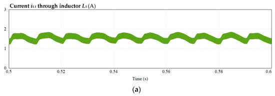
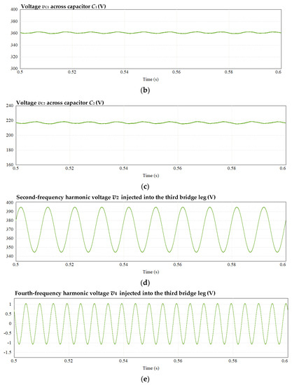
Figure 18.
Simulation waveform with third leg enabled: (a) current of inductor L1, (b) voltage across capacitors C1, (c) voltage across capacitors C2, (d) second-frequency harmonic voltage injected into third bridge leg, and (e) fourth-frequency harmonic voltage injected into third bridge leg.
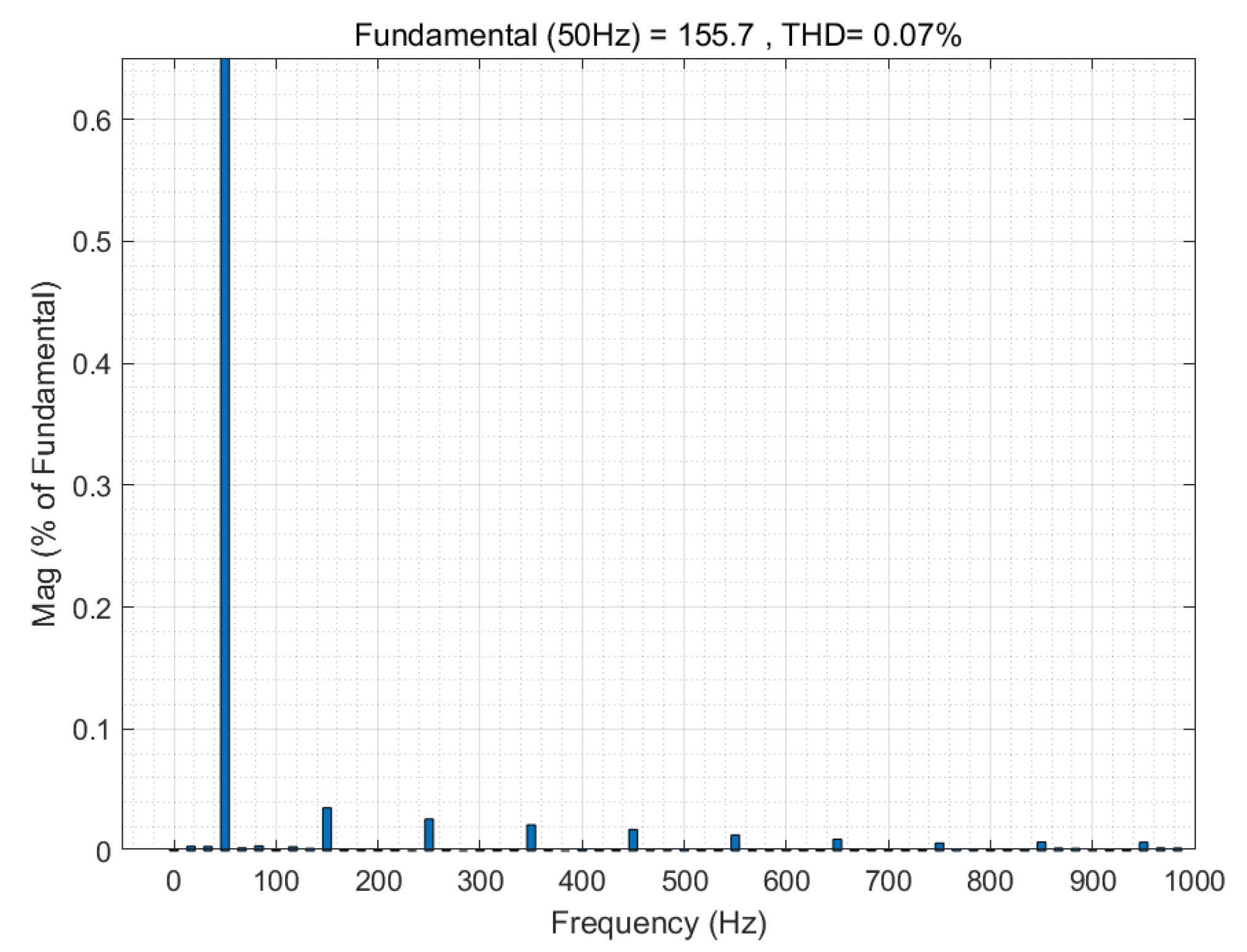
In this case, the FFT analysis of the output voltage is shown in Figure 19, and the THD of the output voltage is only 0.07%.
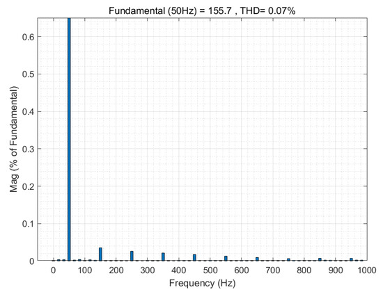
Figure 19.
FFT analysis of output voltage.
Figure 20 shows the comparison of low-frequency current ripple in the input current before and after enabling the third bridge leg under the condition of underload. It can be seen that the low-frequency current ripple in the input current is significantly reduced after enabling the third bridge leg. Specifically, the second harmonic ripple is reduced from 16.2% to 7.6%, and the fourth harmonic ripple is reduced from 16.3% to 4.1%.

Figure 20.
Comparison of low-frequency current ripple in input current before and after enabling the third bridge leg under condition of underload.
5.3. Dynamic Simulation of the System
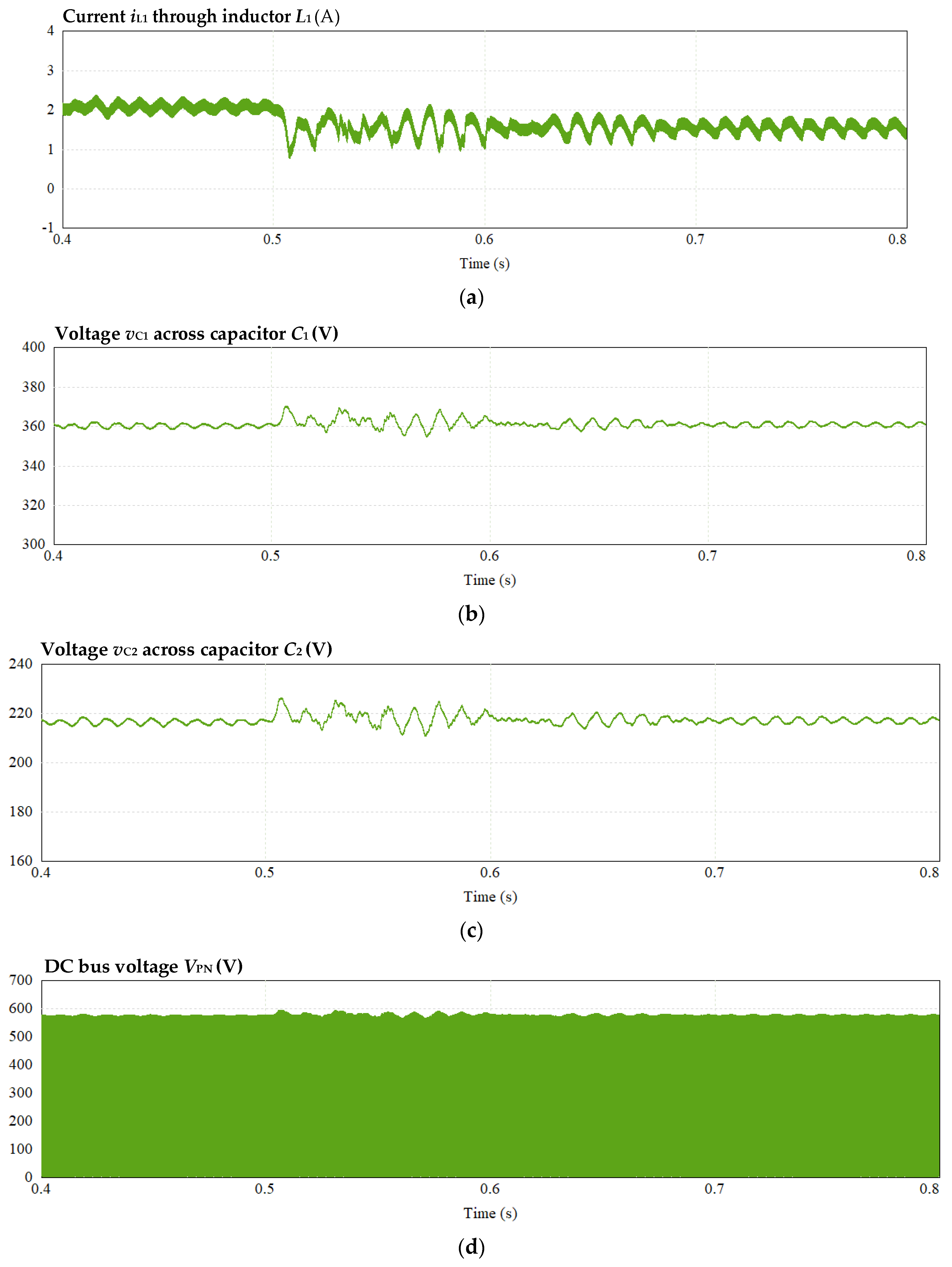
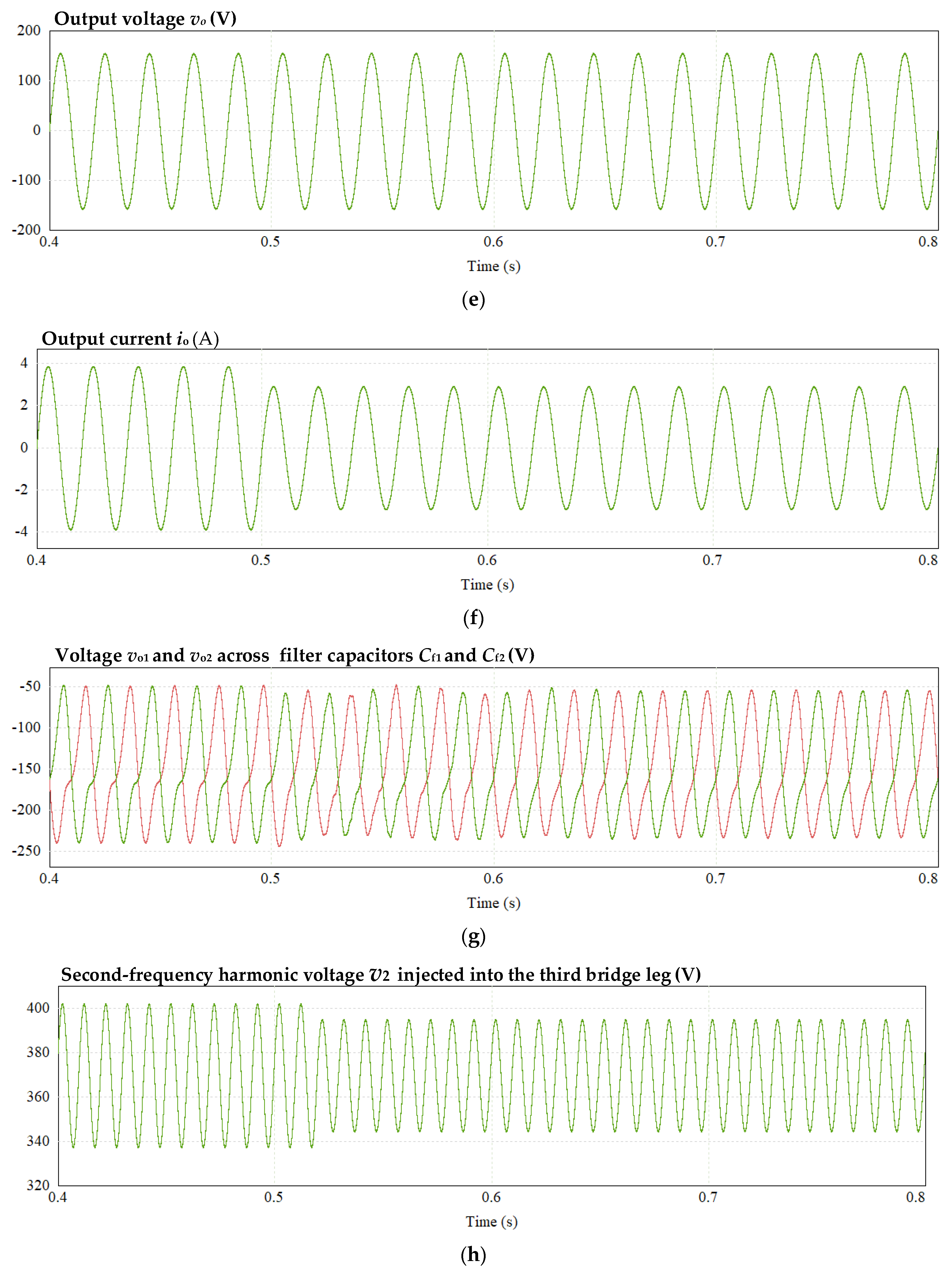
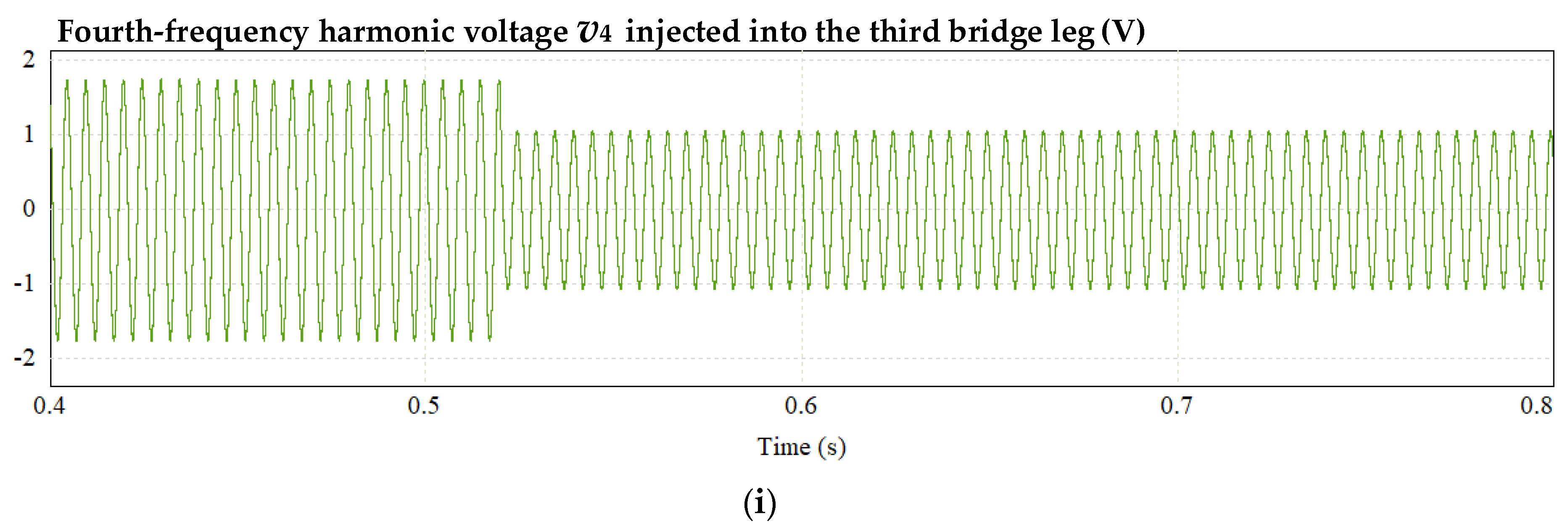
To assess the performance of the circuit under load disturbance conditions, the circuit is simulated from full load to under load with a transition time of 0.5 s. The simulation waveform is depicted in Figure 21. From the simulation waveforms, the following observations can be made:
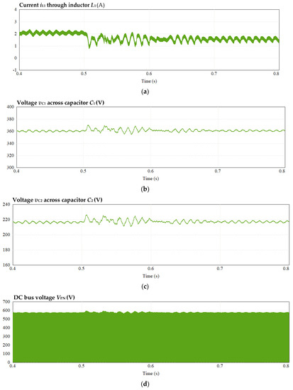
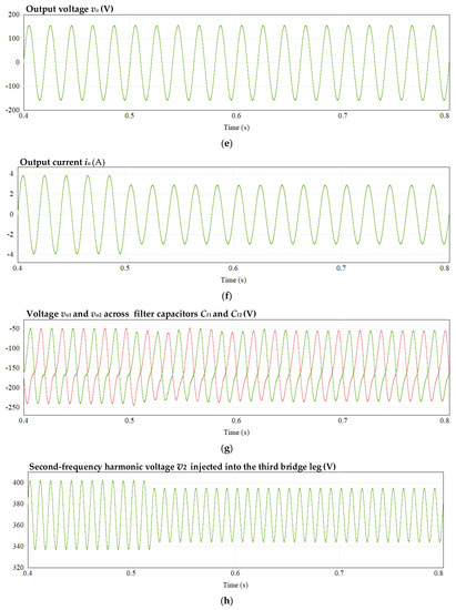
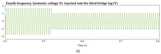
Figure 21.
Dynamic simulation waveform of transition from full load to under load (0.5 s): (a) current of inductor L1, (b) voltage across capacitor C1, (c) voltage across capacitor C2, (d) voltage of DC bus, (e) output voltage, (f) output current, (g) voltage across capacitors Cf1 and Cf2, (h) second-frequency harmonic voltage injected into third bridge leg, and (i) fourth-frequency harmonic voltage injected into third bridge leg.
- (1)
- When transitioning from full load to under load at 0.5 s, the inductor current iL1 of the impedance network stabilizes quickly and maintains good low-frequency ripple suppression capability.
- (2)
- The output voltage vo waveform performs as expected and fluctuates within 1 V, even during the disturbance. The voltage THD remains less than 1% throughout the process, while the output current io smoothly decreases and changes due to the increase in load.
- (3)
- The DC bus voltage VPN remains stable after a short disturbance.
- (4)
- As the output pulsating power decreases after the load changes, the power required to buffer the third bridge leg decreases. Consequently, the amplitude of the second and fourth harmonic voltages V2 and V4 injected using the third bridge leg decreases, and the amplitude of the filter capacitor voltages vo1 and vo2 also decreases.
A comprehensive analysis indicates that the system exhibits good dynamic tracking performance when transitioning from full load to under load.
6. Conclusions
This paper proposes a single-phase quasi-Z-source inverter (QZSI) with an integrated active filter to buffer the output 2ω power through injecting a low-frequency harmonic voltage into the third bridge leg. This method minimizes the 2ω ripple on the DC side and substantially reduces the required inductance and capacitance values of the impedance network. Moreover, the paper presents a comprehensive analysis of the working principle and control methodology of the proposed circuit topology, as well as guidelines for designing its key parameters. When the third bridge leg is activated in the inverter, the simulation results show that the output voltage and current THD are less than 1%, indicating excellent output performance. Under full load condition, the input-side inductor current ripples ΔI from 1.89 A with passive filtering to 0.513 A, representing a reduction of 72.86%, and the DC bus voltage ripples ΔVPN from 70.75 V to 6.54 V, representing a reduction of 90.76%. The second harmonic ripple of the input current is reduced from 18.2% to 4.5%, and the fourth harmonic ripple is reduced from 16.5% to 2.1%. Additionally, the closed-loop control ensures the good dynamic tracking performance of the inverter, while stable control can be achieved in a short time when the load undergoes disturbances, meeting the expected results. As a result, the proposed method only necessitates the inductor and capacitor of the impedance network to handle the switching frequency ripple. This situation significantly reduces the size of the inverter and improves the overall system efficiency. The simulation results validate the accuracy and practicality of the proposed circuit topology. In order to further reduce the volume of the inverter and make it more applicable to relevant fields, the integration of inductors in circuits will be studied in future research.
Author Contributions
Conceptualization, C.Z., C.C. and J.J.; methodology, C.Z., C.C. and J.J.; software, C.Z. and C.C.; validation, C.Z. and C.C.; formal analysis, C.Z. and C.C.; investigation, C.Z. and R.C.; resources, C.Z. and R.C.; data curation, C.Z. and R.C.; writing—original draft preparation, C.Z. and C.C.; writing—review and editing, C.Z.; R.C. and J.J.; supervision, J.J.; project administration, J.J.; funding acquisition, J.J. All authors have read and agreed to the published version of the manuscript.
Funding
This research was funded by Natural Science Foundation of Shandong Province grant number ZR2019QEE004 and Qingdao University-Zhangzhou Kehua Postdoctoral Industry-University Cooperation Project grant number ZZKHBSHCXY 20220601.
Data Availability Statement
Data are contained within the article.
Conflicts of Interest
The authors declare that they have no known competing financial interest or personal relationships that could have appeared to influence the work reported in this paper.
References
- Chen, Y.-C.; Chen, L.-R.; Lai, C.-M.; Lin, Y.-C.; Kuo, T.-J. Development of a DC-Side Direct Current Controlled Active Ripple Filter for Eliminating the Double-Line-Frequency Current Ripple in a Single-Phase DC/AC Conversion System. Energies 2020, 13, 4772. [Google Scholar] [CrossRef]
- Yao, W.-L.; Tang, Y.; Zhang, X.-B.; Wang, X.F.; Loh, P.-C.; Blaabjerg, F. Power Decoupling Method for Single Phase Differential Buck Converter. In Proceedings of the 2015 9th International Conference on Power Electronics and ECCE Asia (ICPE-ECCE Asia), Seoul, Republic of Korea, 1–5 June 2015; pp. 2395–2402. [Google Scholar]
- Singh, B.; Singh, B.-N.; Chandra, A.; Al-Haddad, K.; Pandey, A.; Kothari, D.-P. A Review of Single-Phase Improved Power Quality AC-DC Converters. IEEE Trans. Ind. Electron. 2003, 50, 962–981. [Google Scholar] [CrossRef]
- Zhang, M.; Liu, Y.; Li, D.; Cui, X.; Wang, L.; Li, L.; Wang, K. Electrochemical Impedance Spectroscopy: A New Chapter in the Fast and Accurate Estimation of the State of Health for Lithium-Ion Batteries. Energies 2023, 16, 1599. [Google Scholar] [CrossRef]
- Wang, L.-C.; Xie, L.-C.; Yang, Y.; Zhang, Y.-B.; Wang, K.; Cheng, S.-J. Distributed Online Voltage Control with Fast PV Power Fluctuations and Imperfect Communication. IEEE Trans. Smart Grid 2023. [Google Scholar] [CrossRef]
- Talha, M.; Raihan, S.; Rahim, N.-A. PV inverter with decoupled active and reactive power control to mitigate grid faults. Renew. Energ. 2020, 162, 877–892. [Google Scholar] [CrossRef]
- Jiang, J.-H.; Zhang, T.; Chen, D.-L. Analysis, Design, and Implementation of a Differential Power Processing DMPPT with Multiple Buck–Boost Choppers for Photovoltaic Module. IEEE Trans. Power Electron. 2021, 36, 10214–10223. [Google Scholar] [CrossRef]
- Seth, A.-K.; Singh, M. Second-Order Ripple Minimization in Single-Phase Single-Stage Onboard PEV Charger. IEEE Trans. Transp. Electrif. 2021, 7, 1186–1195. [Google Scholar] [CrossRef]
- Wen, J.-P.; Zhao, D.; Zhang, C.-W. An overview of electricity powered vehicles: Lithium-ion battery energy storage density and energy conversion efficiency. Renew. Energ. 2020, 162, 1629–1648. [Google Scholar] [CrossRef]
- Yuan, J.; Yang, Y.; Blaabjerg, F. A Switched Quasi-Z-Source Inverter with Continuous Input Currents. Energies 2020, 13, 1390. [Google Scholar] [CrossRef]
- Gautam, A.-R.; Fulwani, D.-M.; Makineni, R.-R.; Rathore, A.-K.; Singh, D. Control Strategies and Power Decoupling Topologies to Mitigate 2ω-Ripple in Single-Phase Inverters: A Review and Open Challenges. IEEE Access 2020, 8, 147533–147559. [Google Scholar] [CrossRef]
- Zhou, Y.-L.; Liu, Y.-L.; Su, M.; Sun, Y. A Single-phase Voltage Source Inverter with Lower-Voltage-Rated Capacitor and Ripple Power Decoupling Function. In Proceedings of the 2020 15th IEEE Conference on Industrial Electronics and Applications (ICIEA), Kristiansand, Norway, 9–13 November 2020; pp. 1944–1948. [Google Scholar]
- Dang, H.; Ruan, X.-B. A Current Reference Compensation Scheme for Second Harmonic Current Compensator. In Proceedings of the 2020 IEEE 9th International Power Electronics and Motion Control Conference (IPEMC2020-ECCE Asia), Nanjing, China, 29 November–2 December 2020; pp. 2364–2367. [Google Scholar]
- Huang, X.-Z.; Ruan, X.-B.; Zhang, L.; Liu, F. Second Harmonic Current Reduction Schemes for DC–DC Converter in Two-Stage PFC Converters. IEEE Trans. Power Electron. 2022, 37, 332–343. [Google Scholar] [CrossRef]
- Liu, F.; Ruan, X.-B.; Huang, X.-Z.; Qiu, Y.; Jiang. Y.-Y. Control Scheme for Reducing Second Harmonic Current in AC–DC–AC Converter System. IEEE Trans. Power Electron. 2022, 37, 2593–2605. [Google Scholar] [CrossRef]
- Ellabban, O.; Abu-Rub, H. Z-Source Inverter: Topology Improvements Review. IEEE Ind. Electron. Mag. 2016, 10, 6–24. [Google Scholar] [CrossRef]
- Liu, Y.-S.; Ge, B.; Abu-Rub, H.; Blaabjerg, F. Single-Phase Z-Source\/Quasi-Z-Source Inverters and Converters: An Overview of Double-Line-Frequency Power-Decoupling Methods and Perspectives. IEEE Ind. Electron. Mag. 2018, 12, 6–23. [Google Scholar] [CrossRef]
- Vadi, S.; Bayindir, R.; Hossain, E. A Review of Control Methods on Suppression of 2ω Ripple for Single-Phase Quasi-Z-Source Inverter. IEEE Access 2020, 8, 42055–42070. [Google Scholar] [CrossRef]
- Chub, A.; Vinnikov, D.; Blaabjerg, F.; Peng, F.-Z. A Review of Galvanically Isolated Impedance-Source DC–DC Converters. IEEE Trans. Power Electron. 2016, 31, 2808–2828. [Google Scholar] [CrossRef]
- Liu, Y.; Ge, B.; Abu-Rub, H.; Sun, D. Comprehensive Modeling of Single-Phase Quasi-Z-Source Photovoltaic Inverter to Investigate Low-Frequency Voltage and Current Ripple. IEEE Trans. Ind. Electron. 2015, 62, 4194–4202. [Google Scholar] [CrossRef]
- Zhou, Y.; Li, H.-B.; Li, H. A Single-Phase PV Quasi-Z-Source Inverter with Reduced Capacitance Using Modified Modulation and Double-Frequency Ripple Suppression Control. IEEE Trans. Power Electron. 2016, 31, 2166–2173. [Google Scholar] [CrossRef]
- Cao, X.; Zhong, Q.-C.; Ming, W.-L. Ripple Eliminator to Smooth DC-Bus Voltage and Reduce the Total Capacitance Required. IEEE Trans. Ind. Electron. 2015, 62, 2224–2235. [Google Scholar] [CrossRef]
- Wang, R.-X.; Wang, F.; Boroyevich, D.; Burgos, R.; Lai, R.-X.; Ning, P.-Q.; Rajashekara, K. A High Power Density Single-Phase PWM Rectifier with Active Ripple Energy Storage. IEEE Trans. Power Electron. 2011, 26, 1430–1443. [Google Scholar] [CrossRef]
- Sun, Y.; Liu, Y.-L.; Su, M.; Xiong, W.-J.; Yang, J. Review of Active Power Decoupling Topologies in Single-Phase Systems. IEEE Trans. Power Electron. 2016, 31, 4778–4794. [Google Scholar] [CrossRef]
- Nandi, P.; Adda, R. Integration of Boost-Type Active Power Decoupling Topology with Single-Phase Switched Boost Inverter. IEEE Trans. Power Electron. 2020, 35, 11965–11975. [Google Scholar] [CrossRef]
- Cai, W.; Liu, B.-Y.; Duan, S.-X.; Jiang, L. An Active Low-Frequency Ripple Control Method Based on the Virtual Capacitor Concept for BIPV Systems. IEEE Trans. Power Electron. 2014, 29, 1733–1745. [Google Scholar] [CrossRef]
- Li, L.-Z.; Meng, L.-H.; Zhang, S.; Wang, T.-X.; Shu, Z.-L. ZVS Analysis and Control Strategy for Back-Stage of Single-Phase AC-DC-DC Converter with Low-Frequency DC-Link Voltage Ripple. In Proceedings of the 2021 IEEE 16th Conference on Industrial Electronics and Applications (ICIEA), Chengdu, China, 1–4 August 2021; pp. 1001–1006. [Google Scholar]
- Yu, Y.; Zhang, Q.; Liang, B.; Liu, X.; Cui, S. Analysis of A Single-Phase Z-Source Inverter for Battery Discharging in Vehicle to Grid Applications. Energies 2011, 4, 2224–2235. [Google Scholar] [CrossRef]
- Anderson, J.; Peng, F.-Z. Four Quasi-Z-Source Inverters. In Proceedings of the 2008 IEEE Power Electronics Specialists Conference, Rhodes, Greece, 15–19 June 2008; pp. 2743–2749. [Google Scholar]
- Sun, D.-S.; Ge, B.-M.; Yan, X.-Y.; Bi, D.-Q.; Zhang, H.; Liu, Y.-S.; Abu-Rub, H.; Ben-Brahim, L.; Peng, F.-Z. Modeling, Impedance Design, and Efficiency Analysis of Quasi-Z-Source Module in Cascaded Multilevel Photovoltaic Power System. IEEE Trans. Ind. Electron. 2014, 61, 6108–6117. [Google Scholar] [CrossRef]
- Zhou, Y.; Liu, L.-M.; Li, H. A High-Performance Photovoltaic Module-Integrated Converter (MIC) Based on Cascaded Quasi-Z-Source Inverters (qZSI) Using eGaN FETs. IEEE Trans. Ind. Electron. 2013, 28, 2727–2738. [Google Scholar] [CrossRef]
- Ge, B.-M.; Liu, Y.-S.; Abu-Rub, H.; Balog, R.S.; Peng, F.-Z.; McConnell, S.; Li, X. Current Ripple Damping Control to Minimize Impedance Network for Single-Phase Quasi-Z Source Inverter System. IEEE Trans. Ind. Electron. 2016, 12, 1043–1054. [Google Scholar] [CrossRef]
- Liu, Y.-S.; Ge, B.; Abu-Rub, H.; Sun, H.-X. Hybrid Pulsewidth Modulated Single-Phase Quasi-Z-Source Grid-Tie Photovoltaic Power System. IEEE Trans. Ind. Inform. 2016, 12, 621–632. [Google Scholar] [CrossRef]
Disclaimer/Publisher’s Note: The statements, opinions and data contained in all publications are solely those of the individual author(s) and contributor(s) and not of MDPI and/or the editor(s). MDPI and/or the editor(s) disclaim responsibility for any injury to people or property resulting from any ideas, methods, instructions or products referred to in the content. |
© 2023 by the authors. Licensee MDPI, Basel, Switzerland. This article is an open access article distributed under the terms and conditions of the Creative Commons Attribution (CC BY) license (https://creativecommons.org/licenses/by/4.0/).

