
Global Simulation Model Design of Input-Serial, Output-Parallel Solid-State Transformer for Smart Grid Applications


Abstract
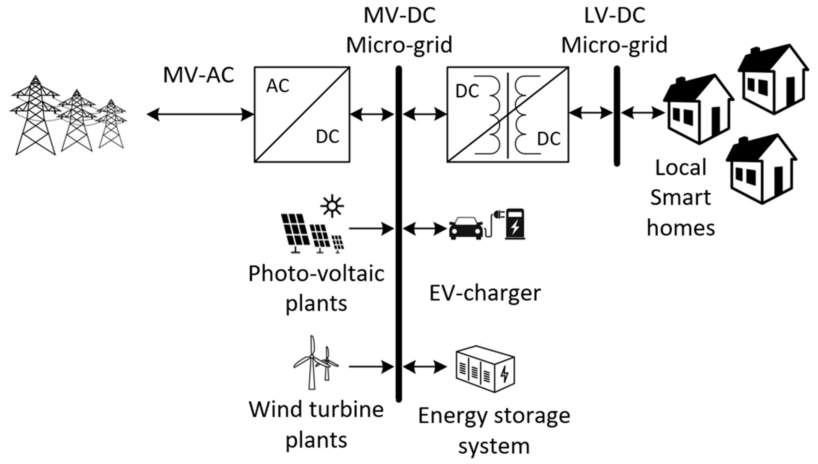
:1. Introduction
2. Materials and Methods
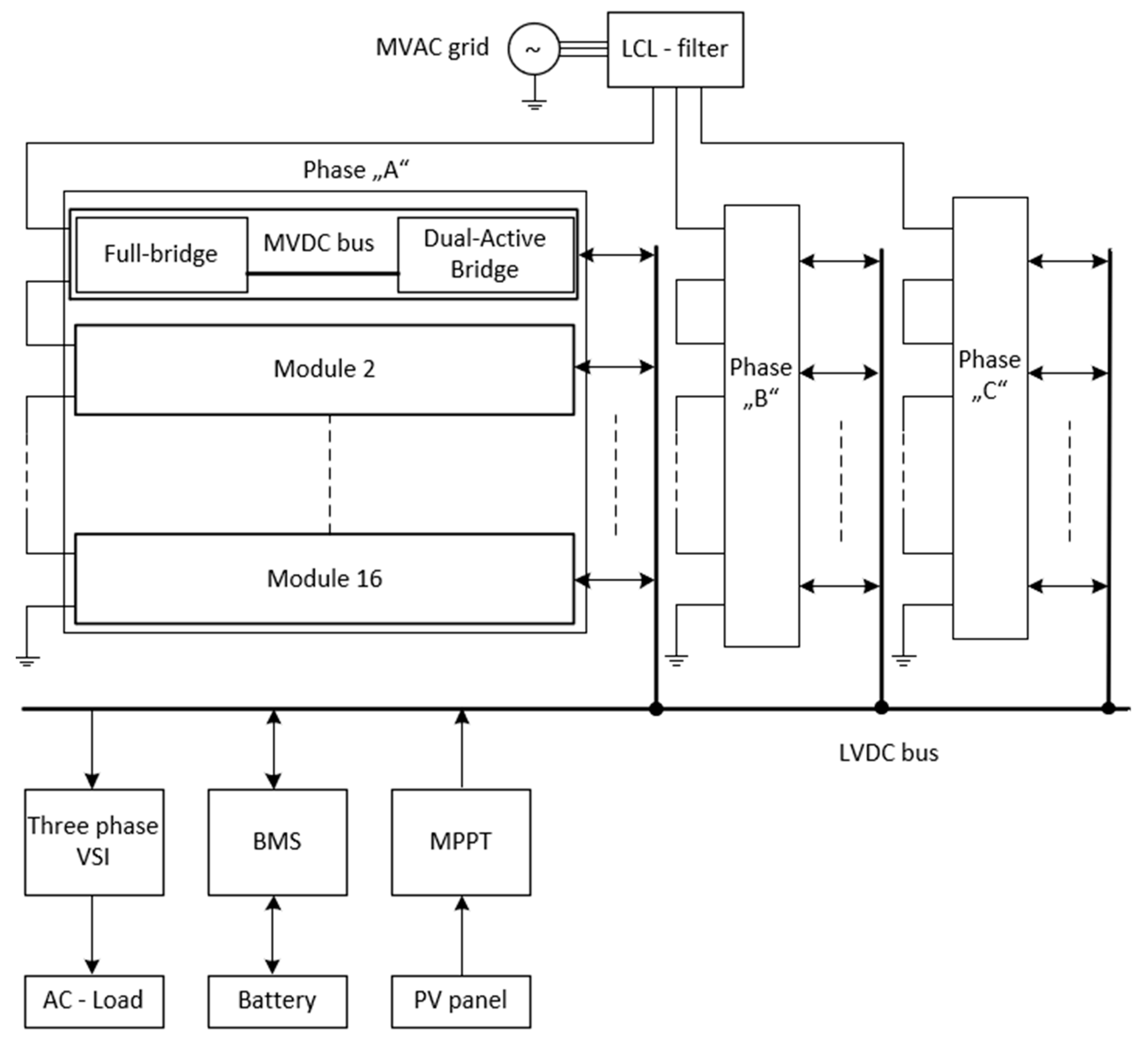
2.1. Medium-Voltage (MV) Stage of SST
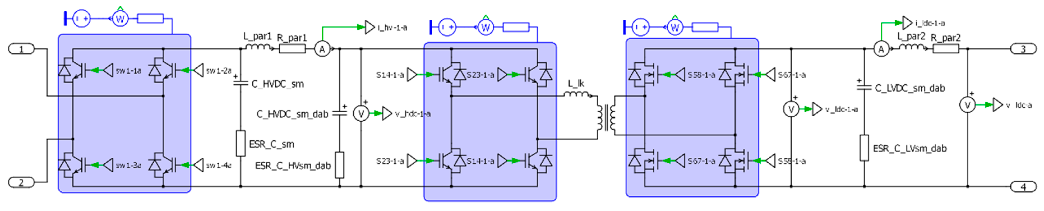
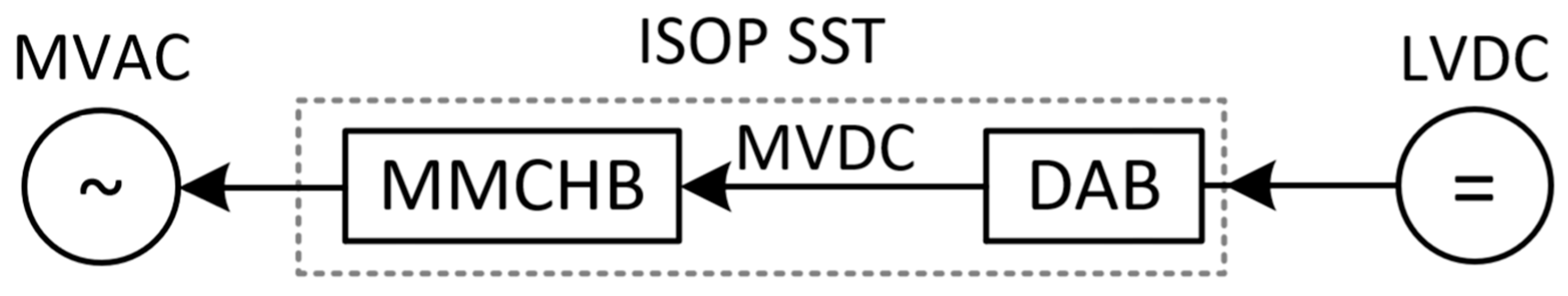
2.2. Isolated Stage of Solid-State Transformer
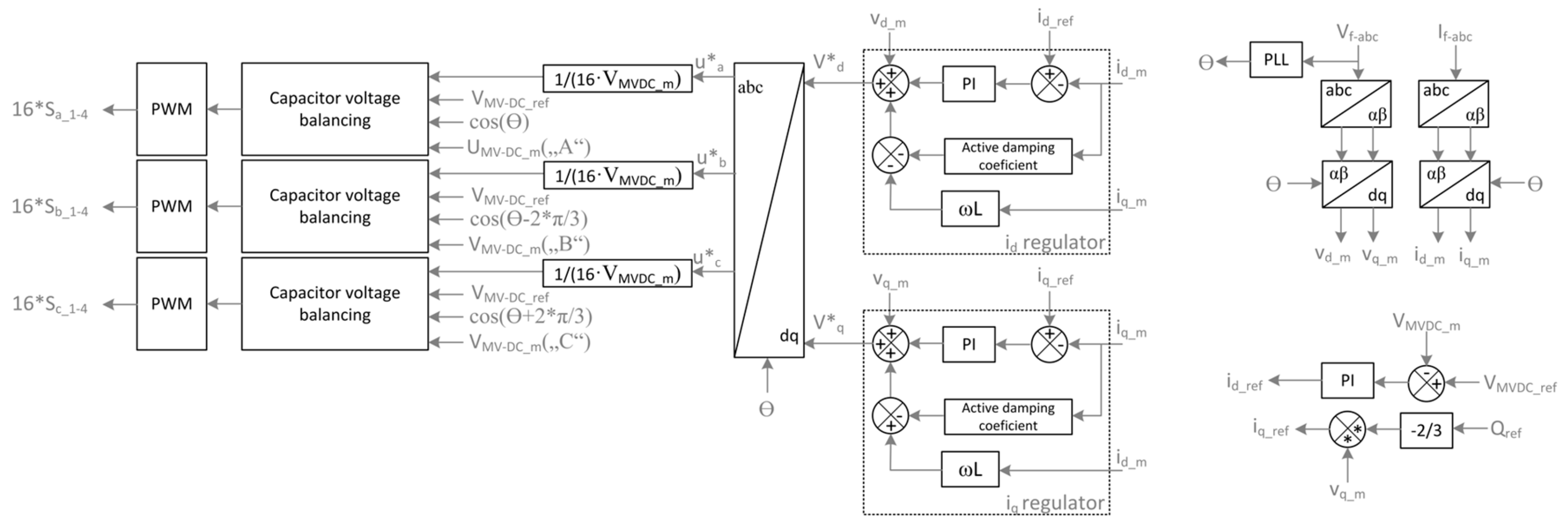
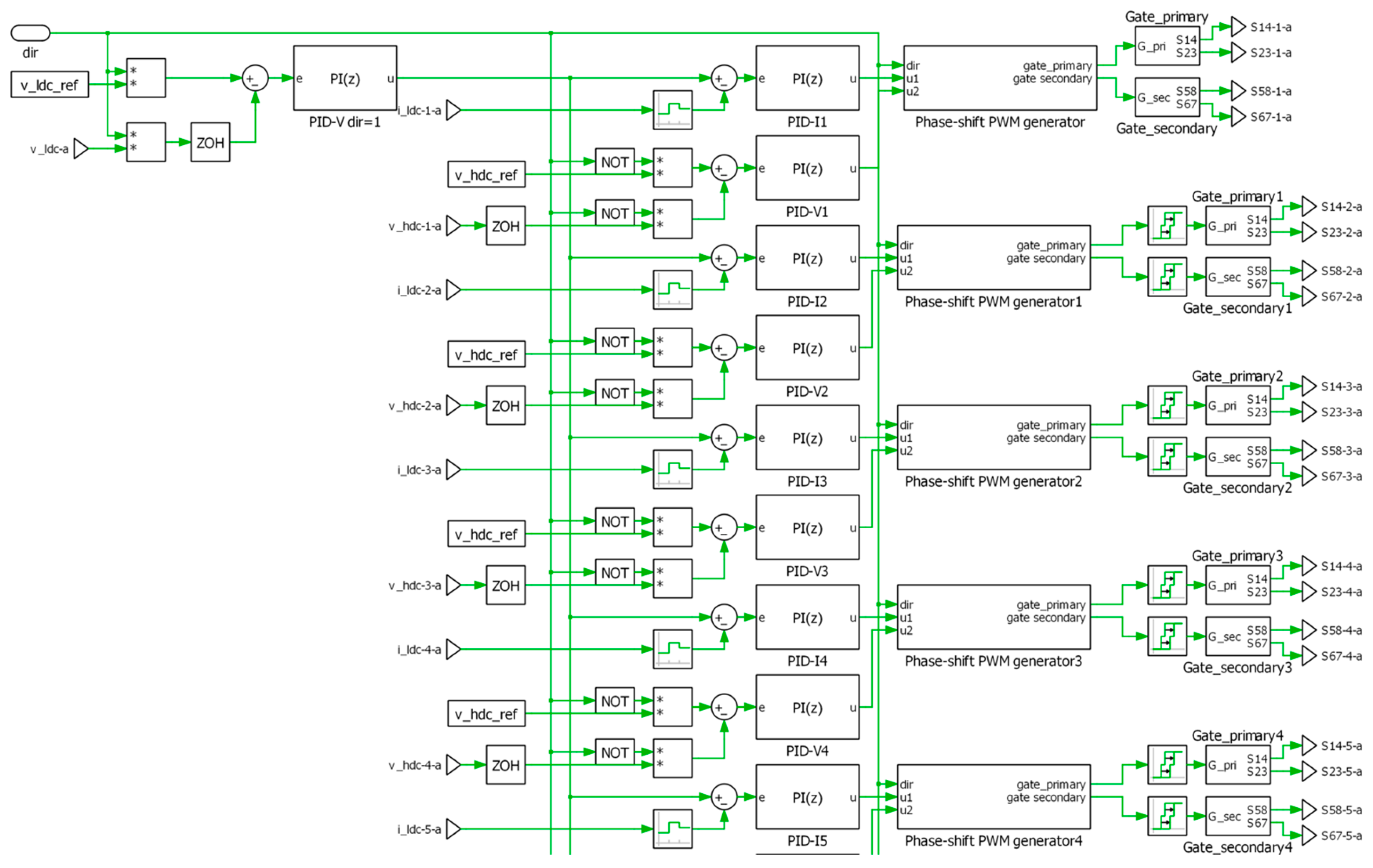
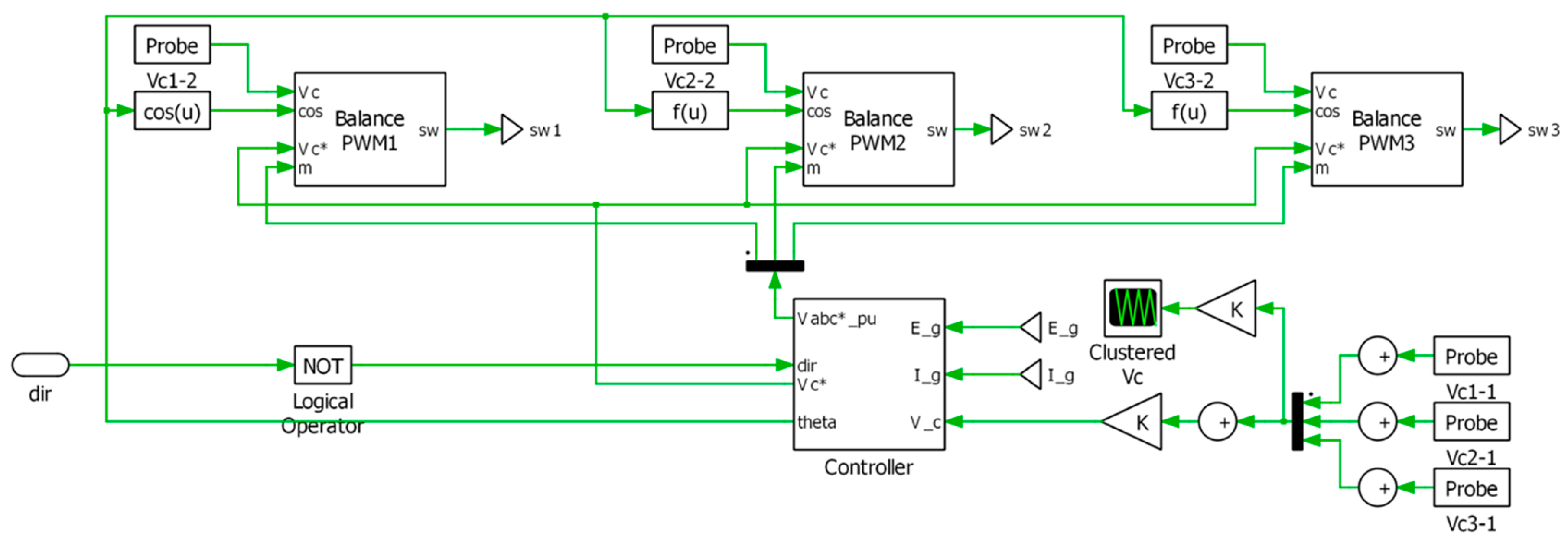
2.3. SST System Control Strategy
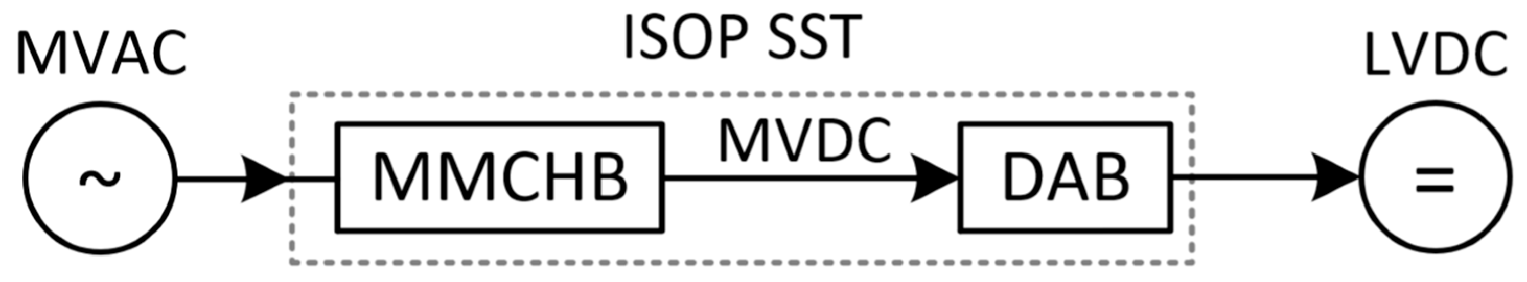
3. Design of Proposed SST Concept
3.1. Design of Medium-Voltage Stage
3.2. Design of Isolated Stage
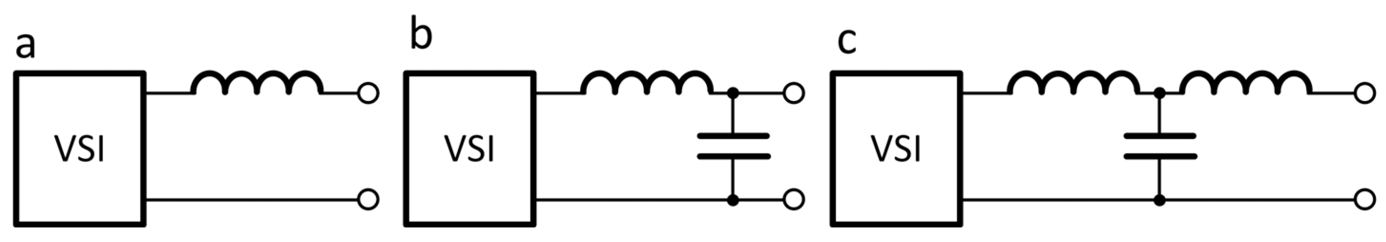
3.3. Filter Design
4. Global Simulation Model Design for HIL Analyses
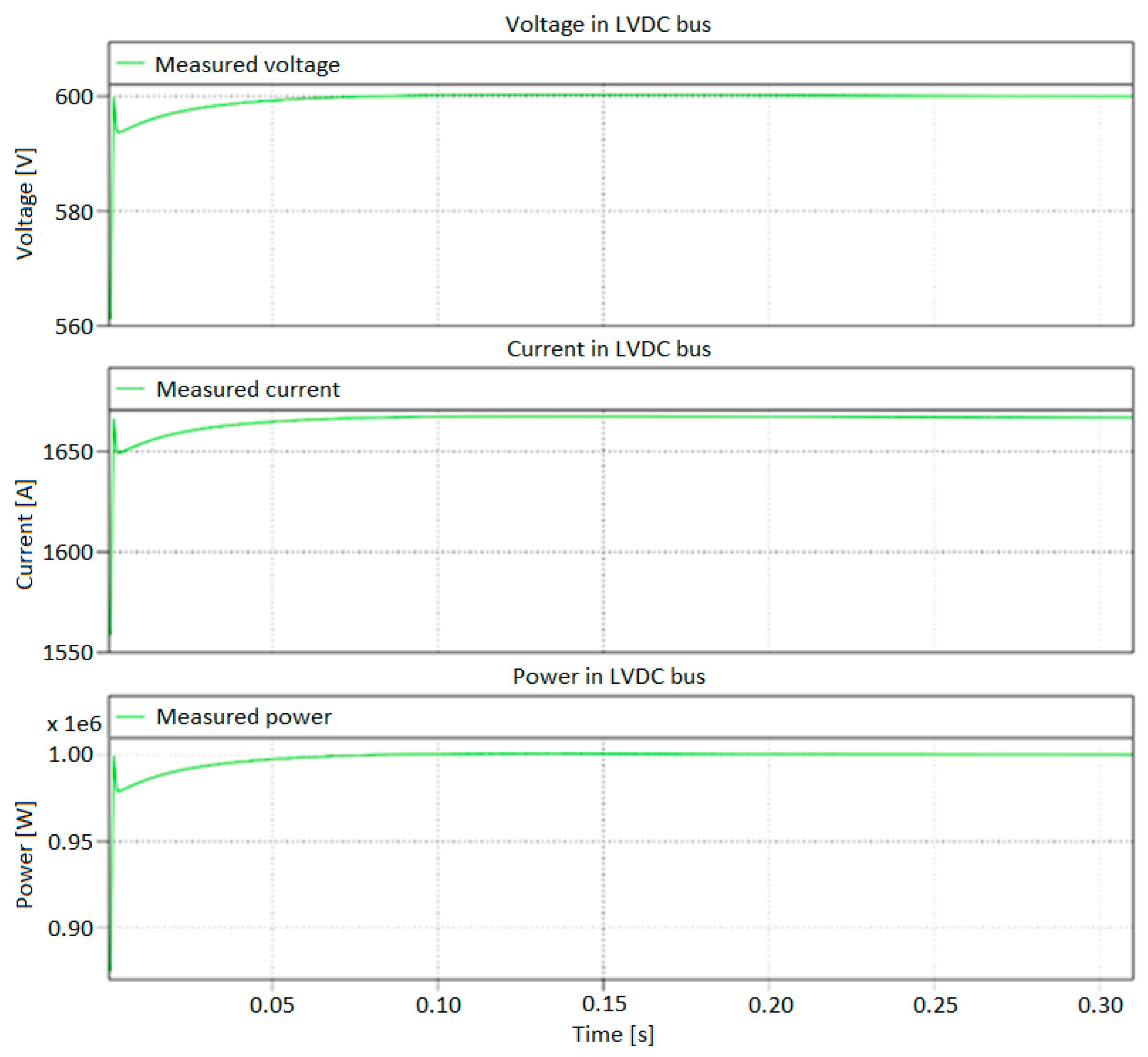
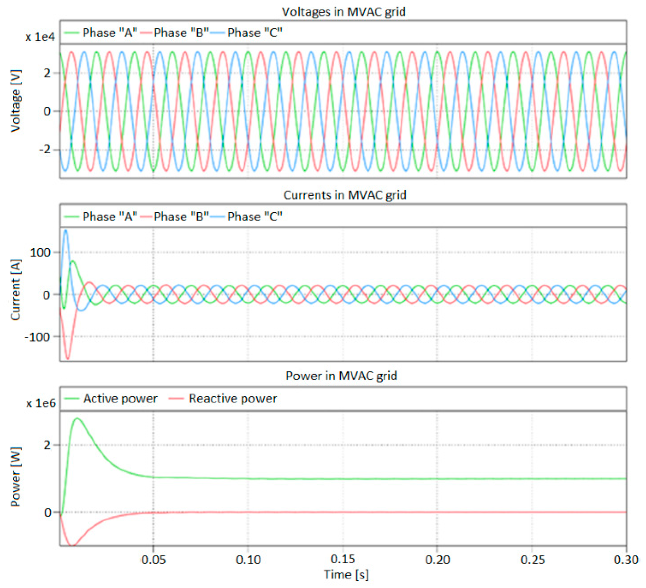
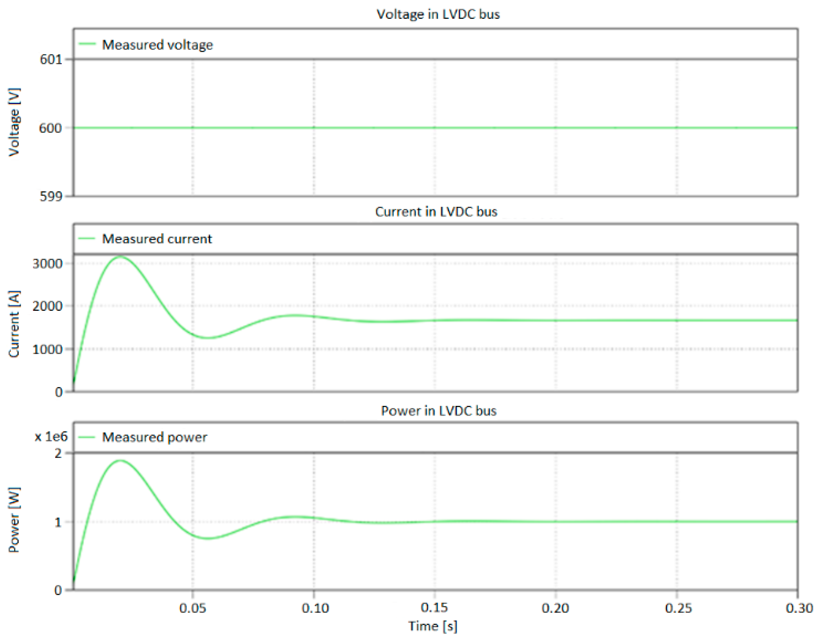
5. Results
6. Conclusions
Author Contributions
Funding
Conflicts of Interest
Abbreviations
| Symbol | Definition |
| AC | Alternating current |
| BMS | Battery management system |
| BSS | Battery storage system |
| DAB | Dual active bridge |
| DC | Direct current |
| DSRF | Decoupled double synchronous reference frame |
| EV | Electric vehicle |
| FB | Full bridge |
| HFT | High-frequency transformer |
| HIL | Hardware-in-the-loop |
| IGBT | Insulated-gate bipolar transistor |
| ISOP | Input-serial output-parallel |
| LVAC | Low-voltage alternating current |
| LVDC | Low-voltage direct current |
| MMC | Modular multilevel converter |
| MMCHB | Modular multilevel cascaded full-bridge |
| MOSFET | Metal–oxide–semiconductor field-effect transistor |
| MPPT | Maximum power point tracking |
| MV | Medium voltage |
| MVAC | Medium-voltage alternating current |
| MVDC | Medium-voltage direct current |
| NPC | Neutral-point-clamped |
| PI | Proportional-integral |
| PLECS | Piecewise linear electrical circuit simulation |
| PLL | Phase-locked loop |
| PSM | Phase-shifted modulation |
| PV | Photo-voltaic |
| PWM | Pulse width modulation |
| RMS | Root mean square |
| SG | Smart grid |
| SPWM | Sine pulse width modulation |
| SRF | Synchronously rotating reference |
| SST | Solid-state transformer |
| THD | Total harmonic distortion |
| VSI | Voltage source inverter |
| WG | Wind generator |
| ZVS | Zero voltage switching |
References
- Hadjsaïd, N.; Sabonnadière, J.C. (Eds.) Smart Grids; John Wiley and Sons: Hoboken, NJ, USA; ISTE: London, UK, 2012. [Google Scholar]
- Momoh, J. Smart Grid. Fundamentals of Design and Analysis; John Wiley and Sons; IEEE Press: Hoboken, NJ, USA, 2012. [Google Scholar]
- Heinemann, L.; Mauthe, G. The universal power electronics based distribution transformer, a unified approach. In Proceedings of the 32nd IEEE Annual Power Electronics Specialists Conference, Vancouver, BC, Canada, 17–21 June 2001; pp. 504–509. [Google Scholar]
- Liu, Y.; Escobar-Mejia, A.; Farnell, C.; Zhang, Y.; Balda, J.C.; Mantooth, H.A. Modular multilevel converter with high-frequency transformers for interfacing hybrid DC and AC microgrid systems. In Proceedings of the 5th IEEE International Symposium on Power Electronics for Distributed Generation Systems (PEDG), Galway, Ireland, 24–27 June 2014. [Google Scholar]
- Alnawafah, H.; Harb, A. Modeling and Control for Hybrid Renewable Energy System in Smart Grid Scenario—A Case Study Part of Jordan Grid. In Proceedings of the 2021 12th International Renewable Energy Congress (IREC), Amman, Jordan, 14–15 April 2021; pp. 1–6. [Google Scholar] [CrossRef]
- Falcones, S.; Mao, X.; Ayyanar, R. Topology comparison for solid state transformer implementation. In Proceedings of the IEEE 2010 PES General Meeting, Minneapolis, MN, USA, 25–29 July 2010; pp. 1–8. [Google Scholar]
- Tan, K.; Yu, R.; Guo, S.; Huang, A.Q. Optimal design methodology of bidirectional LLC resonant DC/DC converter for solid state transformer application. In Proceedings of the IECON 2014—40th Annual Conference of the IEEE Industrial Electronics Society, Dallas, TX, USA, 29 October–1 November 2014; pp. 1657–1664. [Google Scholar] [CrossRef]
- Firouzjaee, M.E.A. Advanced Modeling of Solid State Transformer; Departament d’Enginyeria Elèctrica, Universitat Politècnica de Catalunya: Barcelona, Spain, 2018. [Google Scholar]
- IEC Std 60038; IEC Standard Voltages, Edition 7.0. IEC: Geneva, Switzerland, 2009.
- Kouro, S.; Malinowski, M.; Gopakumar, K.; Pou, J.; Franquelo, L.G.; Wu, B.; Rodriguez, J.; Pérez, M.A.; Leon, J.I. Recent advances and industrial applications of multilevel converters. IEEE Trans. Ind. Electron. 2010, 7, 2553–2580. [Google Scholar]
- Abu-Rub, H.; Holtz, J.; Rodriguez, J.; Baoming, G. Medium-voltage multilevel converters-State of the art, challenges, and requirements in industrial applications. IEEE Trans. Ind. Electron. 2010, 57, 2581–2596. [Google Scholar]
- Rodríguez, J.; Bernet, S.; Wu, B.; Pontt, J.O.; Kouro, S. Multilevel voltagesource-converter topologies for industrial medium-voltage drives. IEEE Trans. Ind. Electron. 2007, 54, 2930–2945. [Google Scholar]
- Frivaldsky, M.; Morgos, J.; Prazenica, M.; Takacs, K. System Level Simulation of Microgrid Power Electronic Systems. Electronics 2021, 10, 644. [Google Scholar] [CrossRef]
- Liserre, M.; Buticchi, G.; Andresen, M.; De Carne, G.; Costa, L.F.; Zou, Z.-X. The smart transformer: Impact on the electric grid and technology challenges. IEEE Ind. Electron. Mag. 2016, 10, 46–58. [Google Scholar]
- Hannan, M.A.; Ker, P.J.; Lipu, M.S.H.; Choi, Z.H.; Rahman, M.S.A.; Muttaqi, K.M.; Blaabjerg, F. State of the Art of Solid-State Transformers: Advanced Topologies, Implementation Issues, Recent Progress and Improvements. IEEE Access 2020, 8, 19113–19132. [Google Scholar] [CrossRef]
- De Silva, H.H.H.; Jayamaha, D.; Lidula, W.A. Review on design and control of solid state transformer based microgrids. AIMS Energy 2019, 7, 901–923. [Google Scholar] [CrossRef]
- Yu, X.; She, X.; Ni, X.; Huang, A.Q. System integration and hierarchical power management strategy for a solid-state transformer interfaced microgrid system. IEEE Trans. Power Electron. 2013, 29, 4415–4425. [Google Scholar] [CrossRef]
- Adabi, M.E.; Martinez-Velasco, J.A.; Alepuz, S. Modeling and simulation of a MMC-based solid-state transformer. Electr. Eng. 2018, 100, 375–387. [Google Scholar] [CrossRef]
- Islam, M.R.; Guo, Y.; Zhu, J. A High-Frequency Link Multilevel Cascaded Medium-Voltage Converter for Direct Grid Integration of Renewable Energy Systems. IEEE Trans. Power Electron. 2014, 29, 4167–4182. [Google Scholar] [CrossRef]
- Marzoughi, A.; Burgos, R.; Boroyevich, D.; Xue, Y. Investigation and comparison of cascaded H-bridge and modular multilevel converter topologies for medium-voltage drive application. In Proceedings of the IECON 2014 40th Annual Conference of the IEEE Industrial Electronics Society, Dallas, TX, USA, 29 October–1 November 2014; pp. 1562–1568. [Google Scholar] [CrossRef]
- Behrouzian, E. Operation and Control of Cascaded H-Bridge Converter for STATCOM Application; Chalmers University of Technology: Gothenburg, Sweden, 2016; Available online: https://www.researchgate.net/publication/301349487_Operation_and_control_of_cascaded_H-bridge_converter_for_STATCOM_application (accessed on 26 May 2022).
- De Doncker, R.; Divan, D.; Kheraluwala, M. A three-phase softswitched high-power-density dc/dc converter for high-power applications. IEEE Trans. Ind. Appl. 1991, 27, 63–73. [Google Scholar]
- Qin, H. Dual Active Bridge Converters in Solid State Transformer. Ph.D. Dissertation, Missouri University of Science and Technology, Rolla, MO, USA, 2012. Available online: https://scholarsmine.mst.edu/doctoral_dissertations/1914 (accessed on 26 May 2023).
- Zumel, P.; Ortega, L.; Lazaro, A.; Fernandez, C.; Barrado, A. Control strategy for modular Dual Active Bridge input series output parallel. In Proceedings of the 2013 IEEE 14th Workshop on Control and Modeling for Power Electronics (COMPEL), Salt Lake City, UT, USA, 23–26 June 2013; pp. 1–7. [Google Scholar] [CrossRef]
- Behrouzian, E.; Bongiorno, M.; De La Parra, H.Z. Investigation of negative sequence injection capability in H-bridge multilevel STATCOM. In Proceedings of the 2014 16th European Conference on Power Electronics and Applications, Lappeenranta, Finland, 26–28 August 2014; pp. 1–10. [Google Scholar] [CrossRef]
- Rachev, E.; Petrov, V. DC link capacitor selection for DC-DC converters. In Proceedings of the 2020 12th Electrical Engineering Faculty Conference (BulEF), Varna Town, Bulgaria, 9–12 September 2020; pp. 1–5. [Google Scholar] [CrossRef]
- El Wahid Hamza, K.A.; Linda, H.; Cherif, L. LCL filter design with passive damping for photovoltaic grid connected systems. In Proceedings of the IREC2015 The Sixth International Renewable Energy Congress, Sousse, Tunisia, 24–26 March 2015; pp. 1–4. [Google Scholar] [CrossRef]
- Ahmed, K.H.; Finney, S.J.; Williams, B.W. Passive Filter Design for Three-Phase Inverter Interfacing in Distributed Generation. In Proceedings of the Compatibility in Power Electronics (CPE), Gdansk, Poland, 29 May–1 June 2007; pp. 1–9. [Google Scholar] [CrossRef]


| Topology | Advantages | Disadvantages |
|---|---|---|
| Cascade H-Bridge | Simple control strategy and simple voltage balance control Modularity | Unachievable MVDC link |
| H-bridge NPC | Lower number of semiconductor switches | Complex control strategy with voltage balance control Limited modularity |
| Multilevel Active NPC | Modularity | Complex control strategy with voltage balance control High amount of clamping diodes |
| Modular Multilevel Converter | Modularity | Complex control strategy with voltage balance control |
| Control algorithms | ||
| Phase-Shifted PWM | Simple control: carrier pairs are assigned to individual cell | Higher losses |
| Level-Shifted PWM | Improved harmonic cancellation | |
| Topology | Advantages | Disadvantages |
|---|---|---|
| Cascade H-Bridge | Simple control strategy and simple voltage balance control Modularity | Unachievable MVDC link |
| Single-phase Dual Active Bridge Converter | Smaller number of passive components Higher efficiency | High RMS DC capacitor currents |
| Three-phase Dual Active Bridge Converter | Lower RMS current Lower ratings of component | Multiple switches and inductors High losses |
| Bidirectional Isolated Current Doubler Topology | Higher currents Small conduction losses Smaller number of switches | Requires more inductors |
| Bidirectional Isolated Push–Pull Topology | High currents Smaller inductor Smaller number of switches | Complex HF transformer |
| Control algorithms | ||
| Phase-Shift Modulation | Simple algorithm | High losses at low power |
| Trapezoidal Modulation | Higher-voltage spectrum | Discontinued operation without load |
| Triangular Modulation | Lower switching losses | Higher RMS currents |
| Control Strategy Type | Control Purpose | Control Algorithms |
|---|---|---|
| Decentralized | Voltage regulation of MVDC bus | Voltage and current dq controller with PWM |
| Bidirectional power flow and power factor correction at MVAC grid | ||
| Voltage regulation of LVDC bus | PSM | |
| Voltage regulation of LVAC grid | D-q controller with SPWM | |
| Capacitor voltage balancing | PI controllers | |
| Centralized | Complex power management | Predictive control algorithm |
| Regulation of DC voltages | Phase-shift method, PWM | |
| Bidirectional power flow | ||
| Voltage regulation on isolation stage | Fuzzy logic | |
| Hierarchical | Primary control layer: decentralized control of each stage of SST | Droop control |
| Secondary control layer: voltage control and management of DC links | Voltage compensation with PI controller | |
| Tertiary control layer: BMS (battery management system), microgrid’s power and fault management | Higher-level control |
| Parameter | Value |
|---|---|
| Pnom | 1 MW |
| VMVAC(RMS) | 22 kV |
| VMVAC(l-l) | 38.105 kV |
| Itotal(RMS) | 45.45 A |
| fsw(MMCHB) | 10 kHz |
| VMVAC(p-p) | 53,889 kV |
| VMVDC_max | 59,278 kV |
| VMVDC_sm_max | 3.7 kV |
| Lg_AC | 5 μH |
| L1f_AC | 55,578 mH |
| L2f_AC | 55,578 mH |
| Cf_AC | 109,611 pF |
| CMVDC_sm | 24,207 μF |
| Parameter | Value |
|---|---|
| Pnom_sm | 20,833 kW |
| Ism_max | 5.63 A |
| VMVDC_sm_max | 3.7 kV |
| fsw(MMCH) | 25 kHz |
| LLK | 86.4 μH |
| CDAB_MVDC_sm | 94.5 pF |
| CDAB_LVDC_sm | 35,957 μF |
| Parameter | Value |
|---|---|
| VLVDC | 600.12 V |
| ΔVLVDC | 0.38 V |
| ILVDC_sm | 1667.09 A |
| ΔILVDC_sm | 0.105 A |
| VMVDC_sm | 3367.92 V |
| ΔVMVDC_sm | 0.782 V |
| IMVDC_sm | 5.631 A |
| ΔIMVDC_sm | 0.612 A |
| VMVAC(RMS) | 22 kV |
| PF | 0.999 |
| celk | 91.68% |
| THDi | 1.779% |
| Parameter | Value |
|---|---|
| VLVDC | 600 V |
| ΔVLVDC | 0.43 V |
| ILVDC_sm | 1633.7 A |
| ΔILVDC_sm | 0.755 A |
| VMVDC_sm | 3369.68 V |
| ΔVMVDC_sm | 4.026 V |
| IMVDC_sm | 6.626 A |
| ΔIMVDC_sm | 1.461 A |
| VMVAC(RMS) | 22 kV |
| PF | 0.999 |
| tot | 92.351% |
| THDi | 1.869% |
Disclaimer/Publisher’s Note: The statements, opinions and data contained in all publications are solely those of the individual author(s) and contributor(s) and not of MDPI and/or the editor(s). MDPI and/or the editor(s) disclaim responsibility for any injury to people or property resulting from any ideas, methods, instructions or products referred to in the content. |
© 2023 by the authors. Licensee MDPI, Basel, Switzerland. This article is an open access article distributed under the terms and conditions of the Creative Commons Attribution (CC BY) license (https://creativecommons.org/licenses/by/4.0/).
Share and Cite
Takacs, K.; Frivaldsky, M.; Kindl, V.; Bernat, P. Global Simulation Model Design of Input-Serial, Output-Parallel Solid-State Transformer for Smart Grid Applications. Energies 2023, 16, 4428. https://doi.org/10.3390/en16114428
Takacs K, Frivaldsky M, Kindl V, Bernat P. Global Simulation Model Design of Input-Serial, Output-Parallel Solid-State Transformer for Smart Grid Applications. Energies. 2023; 16(11):4428. https://doi.org/10.3390/en16114428
Chicago/Turabian StyleTakacs, Kristian, Michal Frivaldsky, Vladimir Kindl, and Petr Bernat. 2023. "Global Simulation Model Design of Input-Serial, Output-Parallel Solid-State Transformer for Smart Grid Applications" Energies 16, no. 11: 4428. https://doi.org/10.3390/en16114428