Abstract
Cu-In-Ga-Se nanoparticles (NPs) were synthesized using a colloidal route process. The effects of growth temperature (GT) on the properties of CuInGaSe2 (CIGS) thin films made from these nanoparticles were investigated using TEM, PL, XRD, and SEM techniques. The Cu-In-Ga-Se NPs were synthesized at growth temperatures ranging from 90 °C to 105 °C and then annealed at 550 °C for 7 min under a Se ambient. The resulting CIGS thin film, formed from Cu-In-Ga-Se NPs synthesized at a GT of 90 °C (referred to as GT90-CIGS), showed a tetragonal structure, large grain size, and high sunlight absorption. It had a band gap energy (Eg) of approximately 0.94 eV. Non-vacuum GT90-CIGS-based solar cells were investigated and fabricated using varying thicknesses of a CdS buffer layer. The maximum power conversion efficiency achieved was approximately 8.3% with an optimized device structure of Al/ITO/ZnO/CdS/CIGS/Mo.
1. Introduction
Chalcogenide nanoparticles (NPs) have recently gained significant attention across various fields [1,2,3]. CuInGaSe2 (CIGS) nanocrystalline films used as hole transport materials in perovskite solar cells, Ga was added to the CIGS compound to control the band gap energy of CIGS NPs and engineer the band alignment in the device’s structure. As a result, the filling factor increased and the recombination rate of the device reduced, leading to an improvement in the device’s efficiency [4]. In particular, CuInGaSe2 compounds are used as the absorption layer in thin-film solar cells due to their suitable band gap (~1.4 eV) and large absorption coefficient (~104 cm−1) [5,6,7]. The deposition of CIGS layers is commonly achieved through vacuum methods such as co-evaporation [8,9,10] and sputtering [11]. These methods offer several benefits, including high efficiency of solar cells, excellent reproducibility, and precise control over composition. However, vacuum-based deposition methods often encounter challenges such as low deposition rates, elevated production costs, and limited availability of the precursor materials. In particular, the choice of precursor materials plays a crucial role in shaping the processes involved in thin film formation. However, non-vacuum methods that employ Cu-In-Ga-Se containing inks, either in a pure liquid form or in a suspension of NPs mixed with solvent, offer certain advantages such as a simple processing sequence, higher growth rates, and lower production cost [12,13,14,15]. However, non-vacuum methods are often associated with challenges such as relatively low cell efficiency and limited scalability. Thus, further advancements are needed in areas such as precursor ink preparation, large-area thin film coating capability, and microstructure control. The preparation of precursor ink stands as a crucial step in the fabrication of non-vacuum-based CIGS thin film solar cells. This is because it determines the level of control and complexity in the subsequent process sequence and microstructure manipulation.
The Cu-In-Ga-Se containing NPs, utilized as inks for thin film deposition, can be synthesized by various methods, including colloidal route and solvothermal route processes. The colloidal route is typically conducted under low-temperature and low-pressure conditions, whereas the solvothermal route operates at high-temperature and high-pressure conditions [6,16]. The CIGS compound was synthesized using a facile one-pot heating method, which showed a high reaction yield of approximately 90%. This method allowed for control over the morphology, composition, nanoparticle size, and band gap energy of the CIGS NPs. The CIGS film was then coated as an absorber layer using a drop coating method. The efficiency of the device was tested, and it achieved the highest power conversion efficiency of 0.59% [17].
In this study, the Cu-In-Ga-Se NPs were synthesized using a colloidal route process, and the thin films were subsequently formed using a spray-coating method. These films were annealed under a Se environment at the temperature of 550 °C. The effects of growth temperature on the optical, structural, and electrical properties of the non-vacuum-CIGS films were thoroughly investigated and characterized using standard characterization techniques. Furthermore, non-vacuum-CIGS-based solar cells were fabricated and measured using a solar simulator technique.
2. Materials and Methods
2.1. Materials
CuCl (Aldrich (St. Louis, MO, USA) 99%), InCl3 (Aldrich 98%), GaCl3 (Aldrich 99.99%), and Se (Aldrich 99.9%) were used as precursor materials and ethyl alcohol (Duksan Extra Pure Grade, C2H5OH), n-propyl alcohol (Duksan Extra Pure Grade, n-C3H7OH), and ethylenediamine (Daejung (Busan, Republic of Korea) 97%, C2H4(NH2)2), and iso-butyl alcohol (Duksan extra pure grade, C4H9OH) were used as solvents. All materials were purchased and used without any purification.
2.2. Preparation of Cu-In-Ga-Se Nanoparticles (NPs)
The Cu-In-Ga-Se NPs were synthesized using a liquid-phase reaction at temperatures ranging from 90 to 105 °C. Precursor materials, including CuCl, InCl3, GaCl3, and Se were employed, while solvents such as ethyl alcohol (C2H5OH), n-propyl alcohol (n-C3H7OH), and ethylenediamine (C2H4(NH2)2) were utilized. CuCl was dissolved in ethyl alcohol, while InCl3 and GaCl3 were dissolved in n-propyl alcohol. These solutions were vigorously mixed with dispersed Se in ethylenediamine. The Cu:In:Ga:Se mole ratio was maintained at a constant ratio of 1.5: 1.05: 0.45: 2, and the reaction pressure was kept at 1 bar with a continuous flow of Ar. The synthesis of CIGS NPs was conducted at various temperatures for a duration of 20 h. Specifically, the growth temperatures for the formation of CIGS NPs were set at 90, 95, 100, and 105 °C, respectively. The resulting precipitates were washed with methanol three times to remove impurities, after which the Cu-In-Ga-Se NPs were then dried to obtain pure Cu-In-Ga-Se NPs.
2.3. Preparation of Cu-In-Ga-Se (CIGS) Thin Film
The as-synthesized nanoparticles were dispersed in iso-butyl alcohol (C4H9OH) to create a precursor ink for thin film deposition. Using the air spray coating method, CIGS films were deposited onto a glass substrate coated with Mo. The deposited CIGS films were subsequently annealed at the temperature of 550 °C for 7 min in a selenium environment using the rapid-thermal annealing technique.
2.4. Characterization
The chemical compositions of the CIGS NPs were analyzed using inductively coupled plasma atomic emission spectrometry (ICP-AES, ICPS-8100, Shimadzu, Korea). Structural and morphological properties of CIGS films were confirmed using X-ray diffraction (XRD, PANalytical MPD, Almelo, The Netherlands), scanning electron microscopy (SEM, EOL JSM—7400F, Yokogushi, Tokyo, Japan), and transmission electron microscopy (TEM, FEI Tecnai G2 F20 S-TWIN, Hillsborough, OR, USA). The optoelectronic properties were examined using photoluminescence spectroscopic methods, employing an Ar-ion laser with a wavelength of 514 nm.
3. Results—Discussion
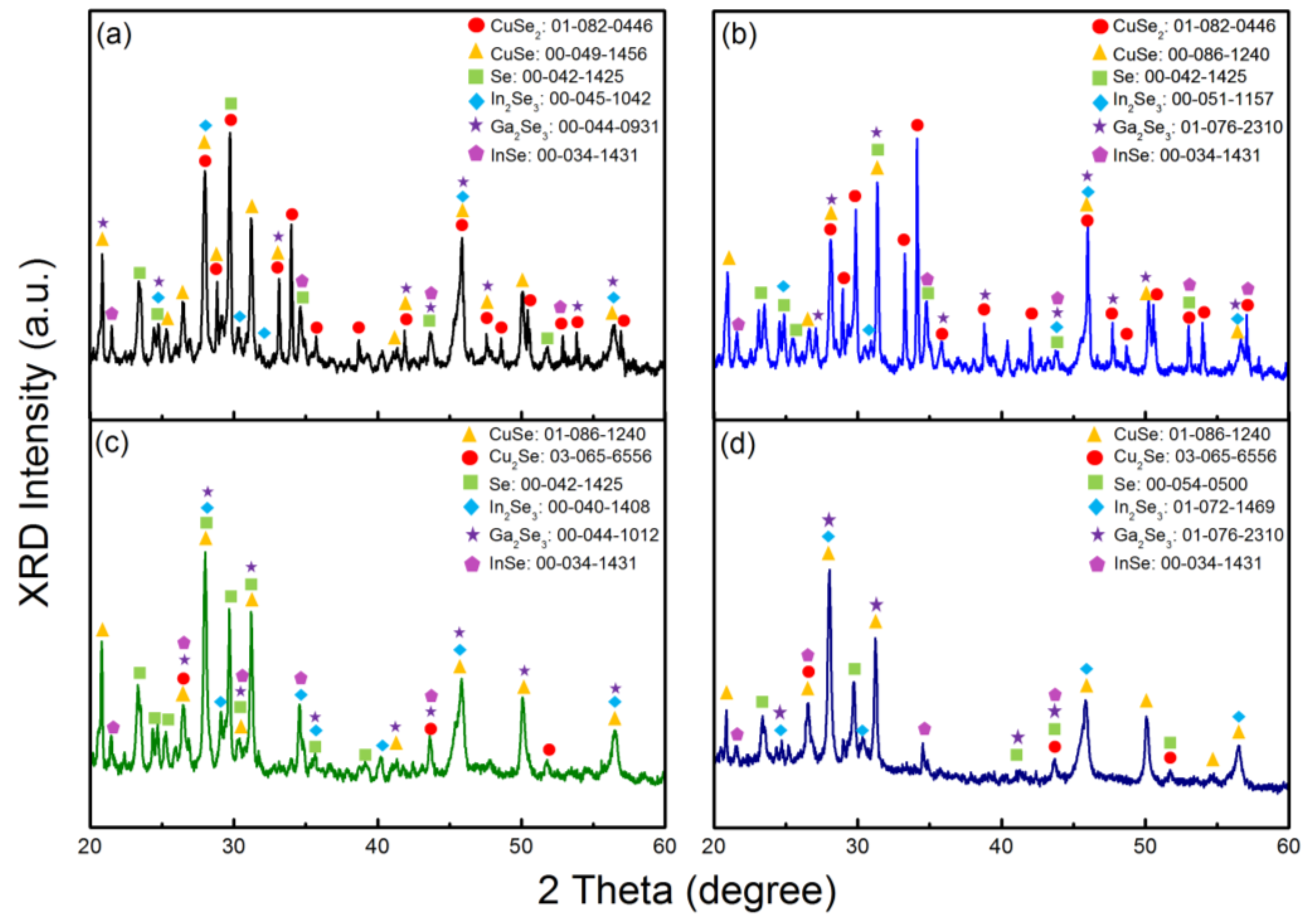
Figure 1 shows the XRD patterns of Cu-In-Ga-Se NPs synthesized at different growth temperatures. The results reveal that the major Cu-Se binary phases of the synthesized nanoparticle at the growth temperature of (a) 90 °C and (b) 95 °C were CuSe and CuSe2, respectively. According to the Joint Committee of Powder Diffraction Standard (JCPDS) card number, the peak of CuSe2 with JCPDS number 01-082-0446 and the peak of InSe with JCPDS number 00-034-1431 were confirmed.
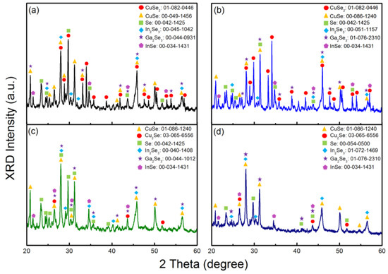
Figure 1.
The X-ray diffraction (XRD) patterns were obtained for Cu-In-Ga-Se nanoparticles (NPs) synthesized at different temperatures: (a) 90 °C, (b) 95 °C, (c) 100 °C, and (d) 105 °C.
However, the main binary phase at the growth temperature of (c) 100 °C and (d) 105 °C was Cu2Se with JCPDS number 03-065-6556. The melting points of CuSe2, CuSe, and Cu2Se were 347 °C, and 550 °C, and 1113 °C, respectively. The Cu2Se phase is unsuitable for forming the CIGS phase upon annealing. The peaks of InSe, In2Se3 (JCPDS number 00-045-1042), Ga2Se3 (JCPDS number 00-044-0931), and Se (JCPDS number 00-042-1425) were also displayed in the XRD spectra with different growth temperatures of 90, 95, 100, and 105 °C. The XRD results showed that the growth temperature can significantly affect the formation of binary phases of the nanoparticles.
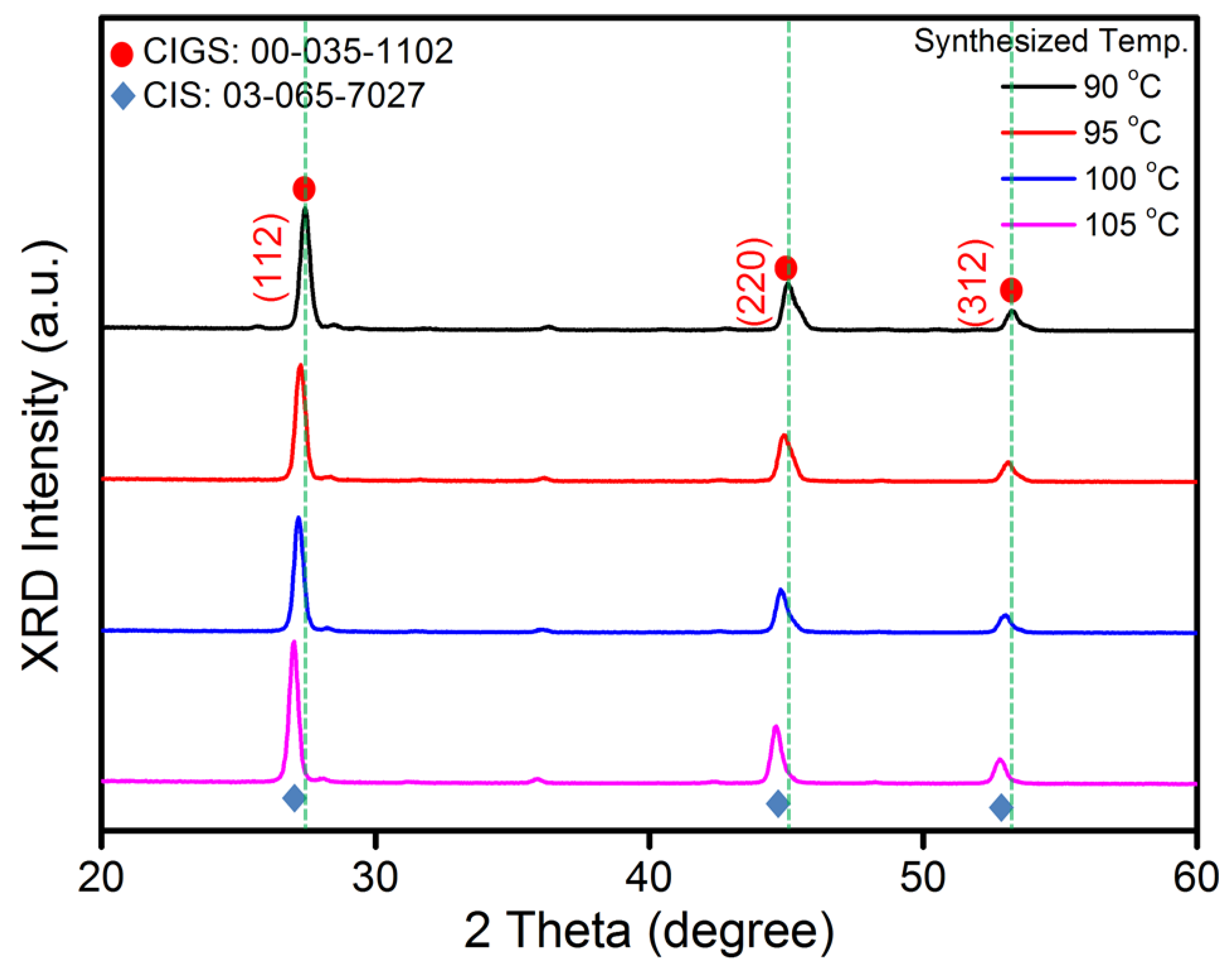
The CIGS films, which were formed by rapid-thermal annealing of Cu-In-Ga-Se precursor ink air-spray coated on substrates, exhibited preferred orientations of (112), (220), and (312), corresponding to the tetragonal phase with a chalcopyrite crystal structure [1,3]. Figure 2 depicts the XRD patterns of the CIGS films obtained using ink containing Cu-In-Ga-Se NPs synthesized at different growth temperatures. The XRD patterns exhibit a shift in the peaks, indicating a higher incorporation of Ga at lower temperatures. Conversely, at higher temperatures, a higher prevalence of pure CIS phases was observed.
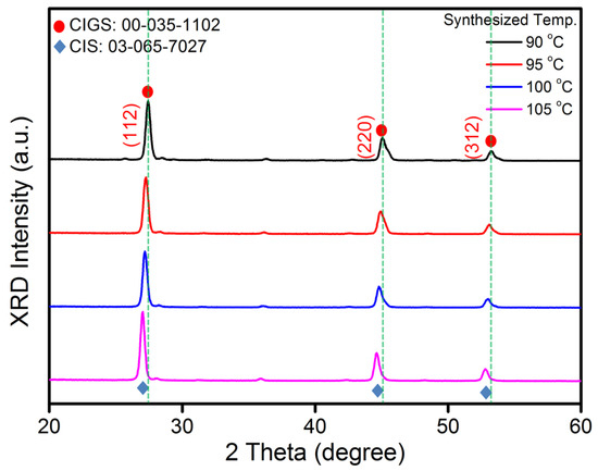
Figure 2.
The X-ray diffraction (XRD) patterns of the CIGS films using Cu-In-Ga-Se nanoparticles (NPs) synthesized at different temperatures.
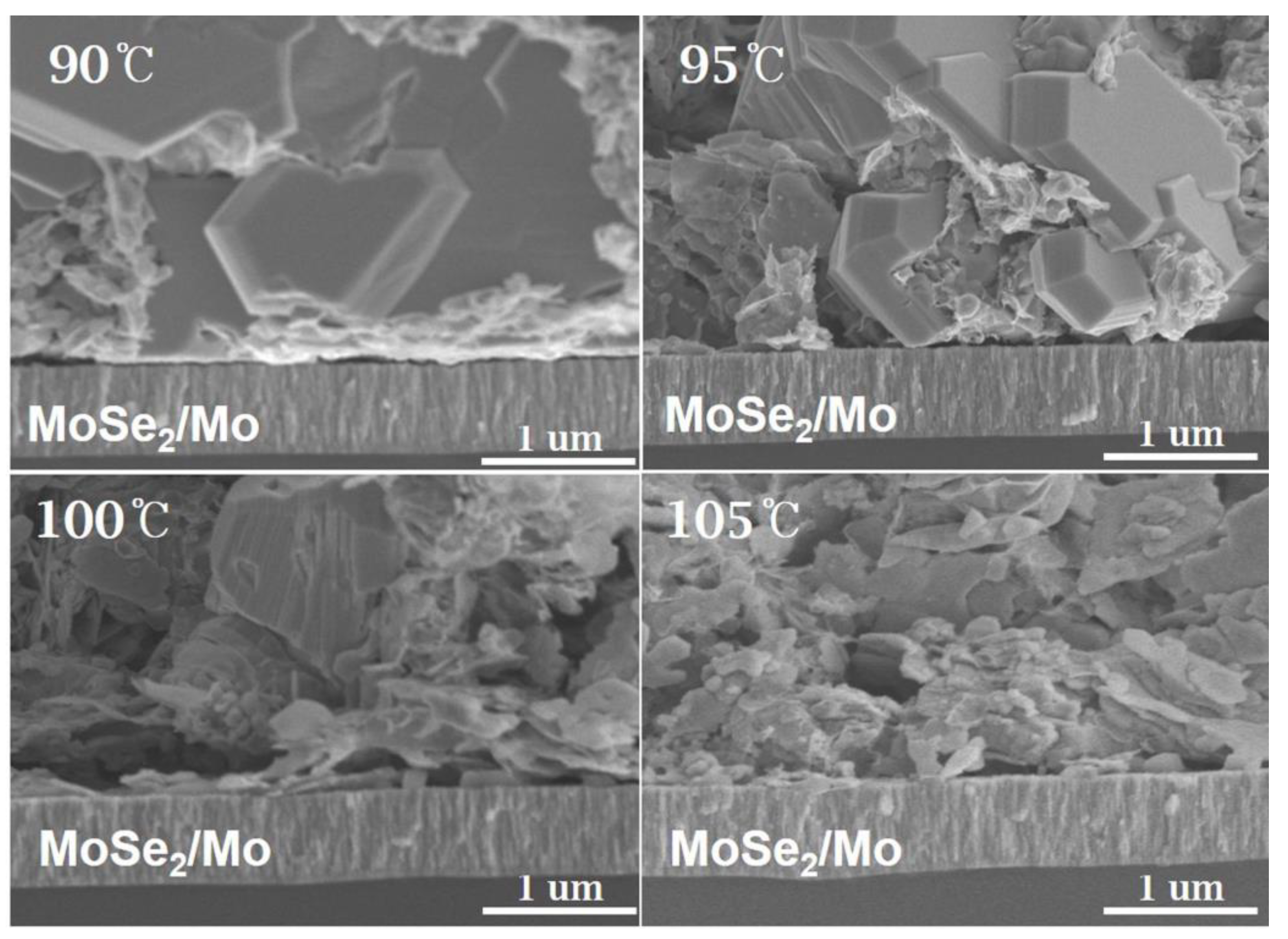
The effects of growth temperature on the morphological properties of CIGS films were investigated by measuring them using SEM techniques. Figure 3 shows the SEM images of CIGS films fabricated from Cu-In-Ga-Se nanoparticles at different growth temperatures. The results indicate that the grain size of CIGS nanoparticles decreased as the growth temperature increased towards 105 °C. Correlating these findings with the XRD results, it was observed that the XRD peak for the (220) direction showed the smallest value at a GT of 90 °C, and the full width at half-maximum of the XRD peak for the (112) direction was the largest value at the GT of 90 °C. The larger grain size observed in the CIGS film synthesized at a growth temperature of 90 °C can be attributed to an enhancement in the crystallization process.

Figure 3.
SEM images of the CIGS films using Cu-In-Ga-Se nanoparticles (NPs) synthesized at different temperatures.
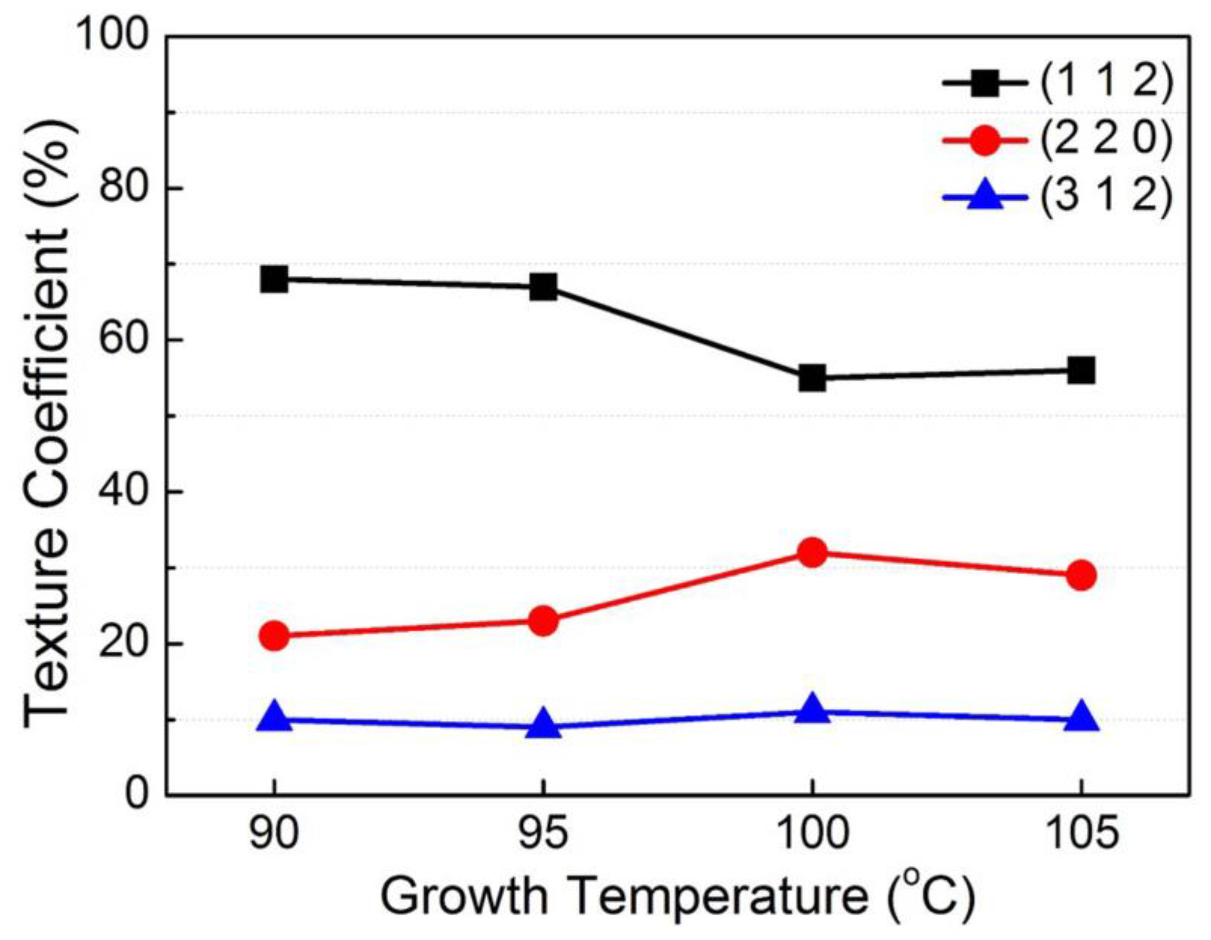
In order to study the effects of growth temperature on the texture and preferred orientation of the CIGS films, the texture coefficients TC(hkl) [15,18,19] was investigated, where
and n is the number of reflections, I(hkl) is the intensity of hkl reflection and Io(hkl) is the intensity of the hkl reflection for a completely random sample. Figure 4 exhibits the texture coefficient as a function of the growth temperature of Cu-In-Ga-Se nanoparticles. The results showed a strong preferred orientation in the (112) direction for all samples. When the growth temperature is increased from 90 to 105 °C, a slight loss of this preferred orientation is observed, which is indicated by a decrease in TC (112) values. However, the TC (220) and TC (312) increased and decreased, respectively, indicating a slight shift in orientation from (112) to the (220) direction. The CIGS film deposited using GT90 nanoparticles exhibited an anomalous, smallest, and broadest (112) peak for any samples in this set. Meanwhile, the (220) peak is hardly visible, indicating a very small grain size structure with a stronger orientation in the (220) direction. These results demonstrate why the electrical and lattice structure of the GT90-CIGS film differs from the other GT95, GT100, and GT105-CIGS films used.
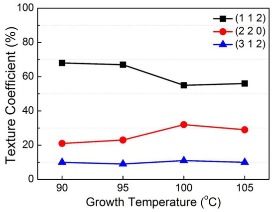
Figure 4.
Texture coefficient of the CIGS films deposited using Cu-In-Ga-Se nanoparticles (NPs) synthesized at different growth temperatures.
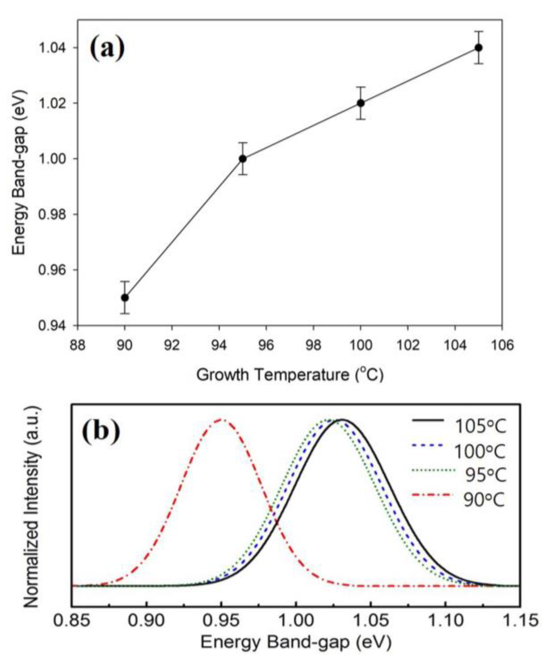
The effects of the growth temperature of Cu-In-Ga-Se nanoparticles on the optical property of formed CIGS film were studied by measuring the photoluminescence, as shown in Figure 5. Figure 5a shows the band gap energy of CIGS film as the function of the GT of nanoparticles. The band gap energy was increased when the GT increased, which might be explained by the reduction of the nanoparticle’s grain size. The grain size decreased when the growth temperature increased, leading to the increase of band gap energy of CIGS film. Figure 5b indicates that the photoluminescence spectra were shifted from a low-bandgap energy region (approximate of 0.94 eV) to a high-band energy region (approximately 1.04 eV due to the reduction of grain size of CIGS films).
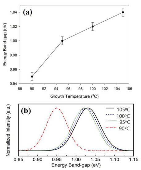
Figure 5.
(a) Bandgap energy diagram and (b) photoluminescence spectra of the CIGS films deposited using Cu-In-Ga-Se nanoparticles (NPs) synthesized at different growth temperatures.
The non-vacuum GT90-CIGS film was chosen as the absorber layer for thin solar cells. Figure 6a depicts the TEM image and size distribution diagram of the Cu-In-Ga-Se nanoparticles synthesized at a growth temperature of 90 °C. The nanoparticles exhibited a monodisperse distribution with a spherical shape, and the average nanoparticle size of nanoparticles was approximately 4.7 nm, with a standard deviation (σ) of 0.763 nm. In Figure 6b, the high-resolution images of the GT90-CIGS film after annealing at 550 °C are presented. The images reveal that the lattice constant of GT90-CIGS films was approximately 5.748 Å. The heat treatment resulted in an improvement in the crystallinity of the nanoparticles.
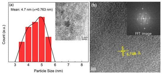
Figure 6.
Transmission electron microscopy (TEM) image and size distribution of Cu-In-Ga-Se (CIGS) nanoparticles synthesized at a temperature of 90 °C (a) displays the size distribution and TEM image of the CIGS nanoparticles (b) shows the TEM image of the CIGS film.
The effects of CdS buffer thickness on non-vacuum (NV) CIGS solar cells were investigated by fabricating a device with a structure of Al/ITO/ZnO/CdS/CIGS/Mo. The GT90-CIGS layer was deposited onto a Mo layer on a soda-lime glass substrate using a spray coating method, with a growth temperature of 90 °C. The resulting films were annealed at 550 °C for 7 min under a selenium environment to facilitate the formation of the CIGS phase. A CdS layer with various thicknesses ranging from 20 nm to 50 nm was formed on the CIGS/Mo film by immersing it into a solution of CdSO4, thiourea (CH4N2S), and NH4OH for different deposition times at 50 °C. The ZnO (thickness, 50 nm) and ITO (thickness, 150 nm) films were then deposited by rf magnetron sputtering. Finally, a patterned aluminum layer for solar cell measurement was deposited using a thermal evaporator.
Non-vacuum CIGS thin-film solar cells were fabricated with varying the CdS buffer’s thickness (T) and were characterized using a Keithley 2400 source meter under simulated AM 1.5G radiation (100 mW/cm2). Figure 7 depicts the J-V curves of the devices as a function of CdS buffer layer thickness of 20, 30, 40, and 50 nm. The T40-CdS device shows an efficiency of approximately 8.3% (Jsc = 15.3 mA/cm2). The T20-CdS, T30-CdS, and T50-CdS devices exhibited efficiencies of 6.4% (Jsc = 14.0 mA/cm2), 7.5% (Jsc = 14.9 mA/cm2), and 5.5% (Jsc = 13.1 mA/cm2), respectively.
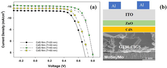
Figure 7.
(a) The J-V curves of the cell with different of the CdS buffer layer’s thickness. Device parameters such as Voc, Jsc, FF, and efficiency from J-V characteristics under illumination at 100 mW/cm2 and (b) the cell’s structure of Al/ITO/ZnO/CdS/CIGS/Mo.
The T40-CdS device exhibited the highest efficiency compared to the T20-CdS, T30-CdS, and T50-CdS devices due to its highest current density of 15.3 mA/cm2 and open-circuit voltage of 0.77 V. The increase in short current density and open-circuit voltage can be attributed to two reasons. Firstly, the absorption loss of light by the CdS layer increases as the thickness of the CdS layer increases from 20 nm to 40 nm. Secondly, the reflectance loss decreases as the thickness of the CdS layer increases from 20 nm to 40 nm [20]. Table 1 shows that both Jsc and Voc values increased with increasing CdS layer thickness until 40 nm, indicating that the CdS/G90-CIGS junction formation was optimized when the CdS buffer layer thickness was 40 nm.

Table 1.
Device parameters such as PCE (power conversion efficiency), Voc (open-circuit voltage), Jsc (short-circuit current density), and FF (fill factor) from J-V characteristics under illumination at 100 mW/cm2.
To further improve device performance, the device fabrication process can be optimized, such as by applying a thermal annealing process and controlling the thickness of the CIGS absorber layer and ITO films. Further investigations will be presented in our future report.
4. Conclusions
The CIGS absorption layers were formed using a non-vacuum method based on Cu-In-Ga-Se nanoparticles (NPs). The effects of the growth temperature during synthesis on the formation of the Cu-In-Ga-Se NPs and the properties of the resulting CIGS film were investigated. The properties of the CIGS films can be controlled by adjusting the synthesis growth temperature of the Cu-In-Ga-Se NPs. The grain size of CIGS thin films decreased with an increase in the growth temperature of the Cu-In-Ga-Se NPs. There was a shift in the XRD peaks and photoluminescence spectra due to the reduction in grain size. The optimized device with a structure of Al/ITO (150 nm)/ZnO (50 nm)/CdS (40 nm)/GT90-CIGS (2 μm)/Mo was fabricated and achieved a maximum power conversion efficiency of 8.3%.
Author Contributions
Writing—original draft preparation, conceptualization, data interpretation, writing—review and editing, H.L.N., H.L. and N.T.N.T.; data curation validation, resources, S.F.S., M.S.T. and H.A.K.; visualization, formal analysis, supervision, J.H.J.; project administration, funding acquisition, J.H.J. All authors have read and agreed to the published version of the manuscript.
Funding
This work was supported by KIST School Partnership Project 2023 for financial support.
Institutional Review Board Statement
Not applicable.
Informed Consent Statement
Not applicable.
Data Availability Statement
Not applicable.
Acknowledgments
The authors extend their sincere appreciation to the Researchers Supporting Project number (RSP2023R370), King Saud University, Riyadh, Saudi Arabia for the financial support.
Conflicts of Interest
The authors declare that they have no known competing financial interest or Personal relationships that could appear to influence the work reported in this paper.
References
- Miskin, C.K.; Deshmukh, S.D.; Vasiraju, V.; Bock, K.; Mital, G.; Camacho, A.D.; Vaddiraju, S.; Agrawal, R. Lead Chalcogenide Nanoparticles and Their Size-Controlled Self-Assemblies for Thermoelectric and Photovoltaic Applications. ACS Appl. Nano Mater. 2019, 2, 1242–1252. [Google Scholar] [CrossRef]
- Nieves, L.M.; Mossburg, K.; Hsu, J.C.; Maidment, A.D.A.; Cormode, D.P. Silver chalcogenide nanoparticles: A review of their biomedical applications. Nanoscale 2021, 13, 19306–19323. [Google Scholar] [CrossRef] [PubMed]
- Guo, Q.; Ford, G.M.; Hillhouse, H.W.; Agrawal, R. sulfide nanocrystal inks for dense Cu(In1−xGax)(S1−ySey)2 absorber films and their photovoltaic performance. Nano Lett. 2009, 9, 3060–3065. [Google Scholar] [CrossRef] [PubMed]
- Khorasani, A.; Marandi, M.; Khosroshahi, R.; Byranvand, M.M.; Dehshani, M.; Zad, A.I.; Tajabadi, F.; Taghavinia, N. Optimization of CuIn1−XGaXS2 Nanoparticles and Their Application in the Hole-Transporting Layer of Highly Efficient and Stable MixedHalide Perovskite Solar Cells. ACS Appl. Mater. Interfaces 2019, 11, 30838–30845. [Google Scholar] [CrossRef] [PubMed]
- Luque, A.; Hegedus, S. Handbook of Photovoltaic Science and Engineering; John Wiley & Sons: Hoboken, NJ, USA, 2022. [Google Scholar]
- Kim, D.; Kim, H.T.; Park, C. Characteristics of CuInSe2 Nanoparticles Synthesized by Se-Redox MethodMol. Cryst. Liq. Cryst. 2012, 565, 32–36. [Google Scholar] [CrossRef]
- Kim, H.T.; Kim, D.; Park, C. Temperature Effects on Cu2ZnSnS4 (CZTS) Films Deposited by Spraying Method. Mol. Cryst. Liq. Cryst. 2012, 564, 155–161. [Google Scholar] [CrossRef]
- Repins, I.; Contreras, M.A.; Egaas, B.; DeHart, C.; Scharf, J.; Perkins, C.L.; To, B.; Noufifi, R. 19·9%–efficient ZnO/CdS/CuInGaSe2 solar cell with 81·2% fill factor. Prog. Photovolt. Res. Appl. 2008, 16, 235–239. [Google Scholar] [CrossRef]
- Lammer, M.; Klemm, U.; Powalla, M. Sodium co-evaporation for low temperature Cu(In,Ga)Se2 deposition. Thin Solid Film. 2001, 387, 33–36. [Google Scholar] [CrossRef]
- Jung, S.; Ahn, S.; Yun, J.H.; Gwak, J.; Kim, D.; Yoon, K. Effects of Ga contents on properties of CIGS thin films and solar cells fabricated by co-evaporation technique. Curr. Appl. Phys. 2010, 10, 990–996. [Google Scholar] [CrossRef]
- Assmann, L.; Bernède, J.C.; Drici, A.; Amory, C.; Halgand, E.; Morsli, M. Study of the Mo thin films and Mo/CIGS interface properties. Appl. Surf. Sci. 2005, 246, 159–166. [Google Scholar] [CrossRef]
- Hibberd, C.J.; Chassaing, E.; Liu, W.; Mitzi, D.B.; Lincot, D.; Tiwari, A.N. Non-vacuum methods for formation of Cu(In, Ga)(Se, S)2 thin film photovoltaic absorbers. Prog. Photovolt. Res. Appl. 2010, 18, 434–452. [Google Scholar] [CrossRef]
- Kaelin, M.; Rudmann, D.; Tiwari, A.N. Low cost processing of CIGS thin film solar cells. Solar Energy 2004, 77, 749–756. [Google Scholar] [CrossRef]
- Kaelin, M.; Rudmann, D.; Kurdesau, F.; Zogg, H.; Meyer, T.; Tiwari, A.N. Low-cost CIGS solar cells by paste coating and selenization. Thin Solid Film. 2005, 480, 486–490. [Google Scholar] [CrossRef]
- Harris, G.B.X. Quantitative measurement of preferred orientation in rolled uranium bars. Phil. Mag. 1952, 43, 113–123. [Google Scholar] [CrossRef]
- Barret, C.S.; Massalski, T.B. Structure of Metals; Pergamon Press: Oxford, UK, 1980. [Google Scholar]
- Latha, M.; Aruna-Devi, R.; Velumani, S.; Murali, B.; Salazar, J.S.; de Mour-Flores, F. Solution based synthesis of Cu(In,Ga)Se2 microcrystals and thin films. RSC Adv. 2019, 9, 35197–35208. [Google Scholar] [CrossRef] [PubMed]
- Jetter, L.K.; McHargue, C.J.; Williams, R.O. Method of Representing Preferred Orientation Data. J. Appl. Phys. 1956, 27, 368. [Google Scholar] [CrossRef]
- Kim, C.; Rhee, I.; Hwang, D.K.; Kim, D.H. Optimum substrate temperature in one-stage co-evaporation of Cu(In,Ga)Se2 thin films for high efficiency solar cells. J. Korean Phys. Soc. 2011, 59, 3432–3435. [Google Scholar] [CrossRef]
- Cho, K.S.; Jang, J.; Park, J.H.; Lee, D.K.; Song, S.; Kim, K.; Eo, Y.J.; Yun, J.H.; Gwak, J.; Chung, C.H. Optimal CdS Buffer Thickness to Form High-Quality CdS/Cu(In,Ga)Se2 Junctions in Solar Cells without Plasma Damage and Shunt Paths. ACS Omega 2020, 5, 23983–23988. [Google Scholar] [CrossRef] [PubMed]
Disclaimer/Publisher’s Note: The statements, opinions and data contained in all publications are solely those of the individual author(s) and contributor(s) and not of MDPI and/or the editor(s). MDPI and/or the editor(s) disclaim responsibility for any injury to people or property resulting from any ideas, methods, instructions or products referred to in the content. |
© 2023 by the authors. Licensee MDPI, Basel, Switzerland. This article is an open access article distributed under the terms and conditions of the Creative Commons Attribution (CC BY) license (https://creativecommons.org/licenses/by/4.0/).

