1. Introduction
Energy harvesting is an alternative way of achieving large autonomy in devices with low power consumption, with the advantage of being maintenance-free. Energy can be defined as a “force” transmitted in the form of matter or waves through a medium such as water, air, or metals [
1]. Energy harvesting is about collecting ambient energy that would otherwise be lost in the form of heat and converting it into electrical energy using a transducer. For example, a photovoltaic (PV) cell converts the energy supplied by a light source into electricity. Harvested energy can be stored or immediately used by small wireless autonomous IoT devices such as those used in wearable electronics, condition monitoring, and wireless sensor networks. The size of the transducer must be compatible with the size of the IoT device, which is generally only a few centimeters. This characteristic limits the amount of energy generated and restricts the application to ultra-low-power devices, typically in the range of nanowatts to microwatts [
2].
Besides light, other types of transducers are used for harvesting energy in the form of vibration, thermal gradient, or RF. The power density of an RF source is highly dependent on the distance from the transmitting device [
3]. RF energy harvesting can be a reliable option for powering a device located in a place with a high concentration of RF signals, such as a city center or commercial building. However, in remote locations where RF signals have low intensity, this may be a poor option. The same occurs with thermal and vibration energy sources. They offer good power density, but are not always available and their application is limited to certain environments [
4].
Light is a commonly used ambient energy source for energy harvesting. Besides being renewable energy, light is abundant in nature and has a very high power density (in the order of 10
W/cm
indoors and 100
W/cm
outdoors [
4]). Photovoltaic cells are common transducers that can be used to harvest energy from indoor and outdoor light. Organic solar cells, including dye-sensitized solar cells (DSSCs), have been recognized as one of the key permanent power source elements for indoor IoT devices [
5].
Harvesters consisting of optical nanoantennae have been proposed as an alternative to the low efficiency of solar cells [
6]. The main obstacles to the use of this type of transducer are the relatively low conversion efficiency and the low-power transfer to the load, both caused mainly by the mismatch between the impedance of the rectifier (several kilohms) and that of the antenna (hundreds of ohms). Some methods have been proposed to overcome this problem [
7].
Conventional amorphous Si solar cells have also been shown to be suitable for energy harvesting, although the low efficiency of about 22% is limited by the material bandgaps of the p–n junction. In [
8], a 42 × 42 mm polycrystalline photovoltaic cell was characterized in an indoor lighting environment with average office illuminance levels provided by LED lamps. At 470 lux and 700 lux, output powers of 23
W and 42
W, respectively, were measured, which are sufficient to feed an ultra-low-power IoT circuit [
9].
Many IoT applications require devices to be self-sufficient and sustainably powered. Most devices are battery-powered due to cost, convenience, size, and the fact that they are deployed in hard-to-reach areas. Battery life must be maximized to avoid battery replacement. In some cases, the battery is completely removed from the system, and the circuit is fully powered by energy harvested from environmental sources. In this case, the circuit must operate with a power consumption compatible with the instantaneous energy harvesting, which is of the order of a few
W [
10].
In batteryless systems, capacitors or supercapacitors can be used to replace batteries as the energy-storing component during the time required to operate the circuit [
11]. In some applications, such as RF transceivers, a very low active-to-sleep duty cycle ratio is expected. In other words, a power-hungry active mode operates for only a small portion of a full cycle, while the remainder of the cycle is spent in a sleep mode to recover the energy consumed [
12]. This type of application can benefit from energy harvesting because the long sleep period is used to recover the energy consumed during the active period.
Newly developed wireless communication protocols such as Bluetooth Low Energy (BLE) [
13,
14], Zigbee [
13,
14], Thread [
15], EnOcean [
16], and Trench [
9] feature extremely low-power scenarios. They can achieve low energy requirements on the order of tens of microwatts for communication in a local area network. This enables the application of indoor-light energy harvesting for batteryless IoT devices, since the power consumption of these circuits is in the same magnitude as the power generated by a small PV cell.
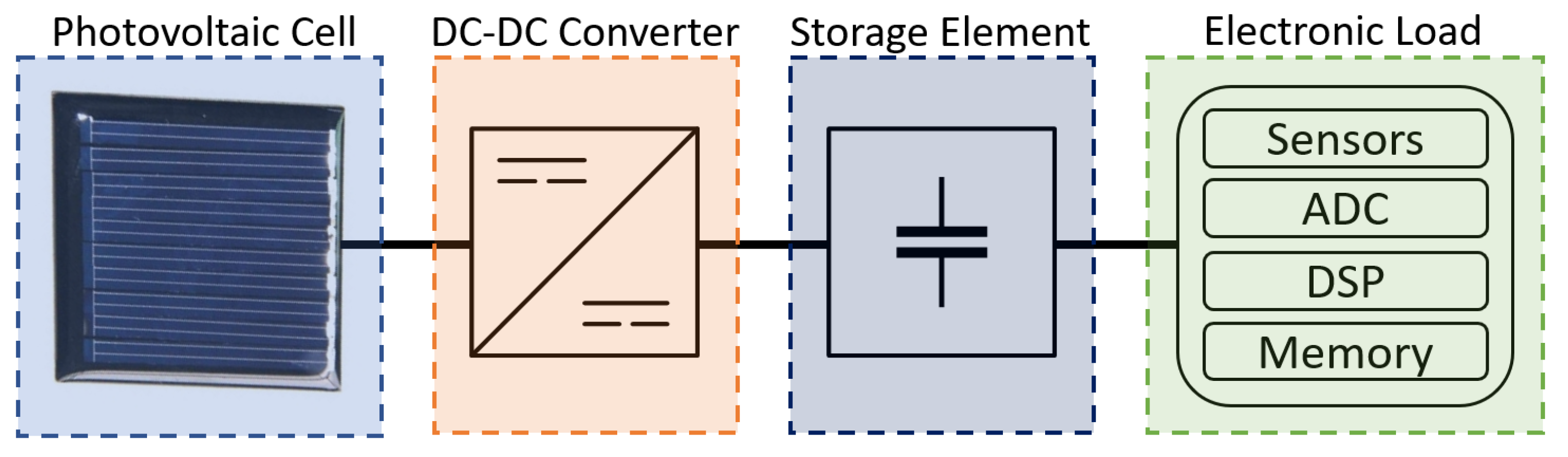
This work focuses on the use of small PV cells to harvest light energy indoors. A typical light-based energy-harvesting system using a PV cell is shown in
Figure 1. It consists of three main components: a transducer, a voltage converter, and an energy storage element. The energy-storing element can be a battery, a capacitor, or a supercapacitor. DC-DC voltage converters are important modules in the energy-harvesting system because they are responsible for producing a functional output voltage from unregulated or non-constant voltage sources, such as the voltage generated by PV cells. A voltage converter is the interface between an unregulated or poorly regulated source and specific voltage rails in an electronic system. Linear converters can be employed for this task, but they are very inefficient because of excessive power loss due to heat. In addition, they function only as buck (step-down) converters, limiting their operation only to higher input voltage levels. In contrast, switched-mode DC-DC converters are very versatile and efficient. Switched-mode converters can be either inductive or capacitive. The inductor-based converter consists of an inductor, a capacitor, and switches, while the capacitor-based converter contains no magnetic component and consists only of capacitors and switches [
17]. In integrated circuits, small areas are often desired for cost reasons, and capacitor-based converters demand less silicon area than inductor-based converters [
18,
19]. For this reason, this work focuses on the development of a switched-capacitor DC-DC converter.
Topologies of switched-capacitor converters have a static ideal voltage conversion ratio (iVCR), a specification that limits the input-output range of the conversion and the efficiency. Multiple topologies can be combined into a single converter with selectable modes to provide greater flexibility in iVCRs and a wider input-output range of upconversion and downconversion [
17]. Another advantage is that the topologies can share flying capacitors to reduce silicon area.
The efficiency of a converter topology decreases when the input or output voltage values cause the VCR (voltage conversion ratio) to deviate from the iVCR. Multitopology converters can improve this by combining multiple conversion ratios.
1.1. Related Works
Various integrated DC-DC converters for different applications are described in the literature. Some DC-DC converter topologies are used in a power management unit (PMU) that converts a fluctuating voltage supplied by a battery into a desired fixed and steady output voltage. They can also be used to provide multiple voltage domains for microprocessor and SoC designs and reduce system power dissipation. For these applications, Naidu and Kittur [
20] and Ghiasi et al. [
21] present different topologies with switched capacitors, but they only perform downconversion. The work of Manohar and Balsara [
22] follows the same buck conversion approach and presents a partially integrated buck DC-DC converter. A different approach is presented by Souvignet et al. [
23] using a more versatile and fully integrated switched-capacitor converter for down and up conversions.
In the field of energy harvesting, a study conducted by Goeppert and Manoli [
24] addressed the development of an inductive DC-DC boost converter that uses temperature differences to harness energy through thermoelectric generators. Chowdary et al. [
25] investigated the implementation of a modular power management system that includes a DC-DC buck-boost inductor-type converter capable of simultaneously harvesting energy from three different sources: solar, vibration, and RF. In their research, Mondal and Paily [
26] introduced an efficient on-chip switching power supply converter for solar energy harvesting that eliminates the need for an on-chip inductor. They proposed a tree-like charge-pump circuit to amplify the voltage obtained from the PV cell and transfer the energy to an energy buffer, such as a supercapacitor or rechargeable battery. Dini et al. [
27] employed a DC-DC buck-boost converter with an off-chip inductor as a fully autonomous integrated circuit (IC) to harvest energy from various sources, including piezoelectric, photovoltaic, thermoelectric, and RF transducers. Chen et al. [
28] integrated a step-up switched capacitor into a compact single-chip IC for solar energy harvesting. This IC used parallel-connected photodiodes as on-chip solar cells and was specifically designed for biomedical implant applications. Megahed and Anand [
29] proposed a switched-capacitor-based solar energy harvester with integrated maximum power point tracking (MPPT) for ultra-low-power applications. Their design achieves the same charge redistribution loss (CRL) as a cross-coupled DC-DC converter, but with only half as many capacitors as needed. Kukunuru et al. [
30] suggested a method in which the PV cells of a series of solar strings are periodically connected in parallel to balance their voltages and extract the maximum available power, even under the presence of mismatch conditions.
Chen et al. [
31] introduces a solution that eliminates the need for batteries, employing a DC-DC boost converter architecture with an off-chip inductor specifically created for applications involving thermoelectric energy harvesting. Devaraj et al. [
32] presents a multitopology converter with 11 iVCRs, from 1/3 to 11/3. This converter is designed for multiple inputs, in this case a piezoelectric generator and a photovoltaic panel. Each source has its own converter block, which contains two multitopology converters, one for integer values of 1, 2, and 3 and one for fractional values of 1/3 and 2/3. It also has an adder topology to sum the fractional and integer converters to obtain a new iVCR.
Cheng et al. [
12] presents a redistributable SC converter for batteryless IoT devices. It consists of 16 charge-pump submodules with iVCRs of 1.5 and 2 and a low-dropout regulator (LDO) to reduce excess voltage. The submodules redistribute in two stages depending on the operating mode (sleep and active).
1.2. Contribution
Although most of the related works propose a feedback loop to control the output voltage by selecting the proper VCR, none of them consider the adjustment of the equivalent output resistance as a control parameter. This technique is explored in this work, in which the equivalent impedance of the DC-DC converter is modeled considering the internal resistance of the energy source (in this case a PV cell).
Recent advances in the development of ultra-low voltage circuits with supply voltages from 400 mV down to 150 mV enabled the development of many electronic circuits such as amplifiers [
33,
34], voltage references [
35], analog filters [
11,
36], data converters [
37,
38,
39], integrated sensors [
40], and microprocessors [
41]. However, harvesting energy from the environment and providing such a controlled supply voltage remains a challenging task.
Considering autonomous applications, the goal of this work is to describe the design of a DC-DC integrated converter used for energy harvesting from indoor light to power a batteryless IoT system. The output voltage is regulated to 400 mV, independent of the input voltage generated by the PV cell. To regulate the output voltage to a fixed value, an on-the-fly tuning of the equivalent output resistance is performed. This tuning is achieved by varying the switching frequency in the switched-capacitor converter. The main contribution is the application of this technique to an ultra-low-power and ultra-low voltage system with an artificial-light-driven PV cell as the power source, where the power levels are in the range of tens of W. The output level of 400 mV was set aiming at ULV applications such as those previously stated. Since this voltage is in the range of the threshold voltage of CMOS transistors, extra design complexity is imposed, which will be described later in the paper.
The main contributions of this work are outlined as follows:
The modeling of the equivalent output resistance including the internal resistance of the PV cell is presented;
The complete electrical design of an integrated circuit in a 180 nm technology containing a regulated DC-DC converter for ultra-low-power and ultra-low voltage applications is described;
The output voltage regulation by tuning the equivalent output resistance through an on-the-fly changing of switching frequency is demonstrated for ultra-low voltage applications;
The design of a cold-start system with a low input voltage of 231.5 mV in a start-up time of only 30.7 s is presented;
The application of indoor-light energy harvesting using small PV cells for batteryless ultra-low voltage circuits is demonstrated.
The remaining of this paper is organized as follows:
Section 2 presents the modeling of the equivalent output resistance of a switched-capacitor converter, including the source resistance;
Section 3 describes the electrical implementation of the proposed integrated DC-DC converter;
Section 4 discusses the obtained results; and finally,
Section 5 summarizes the main conclusions.
2. Modeling the Equivalent Output Resistance
There are some state-of-the-art techniques for modeling SC converters in the literature. Charge flow analysis is a method that provides very accurate results using the asymptotes of the Slow Switching Limit (SSL) and Fast Switching Limit (FSL) to model the equivalent output resistance (
) [
17,
42]. However, this method does not take into account the effects of the source resistance
. In addition, the inclusion of
for modeling
in SC converters may have lower accuracy when higher values of
are considered.
The purpose here is to present an accurate method for modeling the equivalent output resistance of SC converters when a significant source resistance is present at the converter input. The proposed method is based on the inclusion of in the FSL equation.
Figure 2 shows a generic DC-DC voltage converter with a PV cell connected at the input. The simplified equivalent circuit of the PV cell is called the 1D1R model and consists of a current source, a diode, and a series resistor (
) [
43]. The electrical properties of the PV cell change dynamically as a function of illuminance [
44]. For example,
can vary from 2 k
to 2.8 k
when the illuminance in a commercial PV cell of 20.2 cm
changes from 700 lux to 400 lux [
8].
The generic voltage converter can be modeled analogously as an ideal transformer with an output resistance
[
42]. The transformer voltage ratio (1:N) corresponds to the ideal Voltage Conversion Rate (iVCR) of the converter [
17]. The resistance
corresponds to an impedance of
in series with
on the secondary side due to the impedance conversion effect of the transformer. The transformer-based (TR-based) equivalent output resistance (
) is given by:
The series resistance at the converter input significantly affects
, especially at higher values of iVCR. This effect is even worse in cascaded converter stages [
45].
2.1. Charge Flow Analysis
Charge flow analysis is used to determine the individual amounts of charge flowing in each switch and capacitor of the SC converter [
42]. The analysis is performed for each topological state using Kirchhoff’s current law (KCL) to obtain the normalized charge multipliers
, as shown in Equation (
2), where
is the charge flow in component
i during state
j and
is the charge delivered to the output.
Due to the principle of electric charge conservation, the sum of all individual charges in each component should be zero [
17]. The charge flow analysis is divided into two modes: slow and fast switching limits. The SSL occurs when the switching frequency is slow enough that the charge in each flying capacitor fully equalizes at each state. For this reason, finite resistances of switches and capacitors are ignored because they are not large enough to prevent capacitors from being fully charged [
42]. In FSL, the on-state resistances of switches are large enough that flying capacitors cannot reach equilibrium during a switching period [
17,
42].
As an example, consider the circuit of a voltage doubler shown in
Figure 3. In the topological state
, the charge
flows from the voltage source to the flying capacitor
. In the topological state
,
is connected in series with the input voltage, and the charge
flows from
to the buffer capacitor
.
In SSL mode, the resistances of all components are ignored when extracting the vectors of the capacitor charge multipliers. The vectors are given by Equation (
3), where
,
and
are the charge multipliers in state
j for the output,
and the input, respectively, resulting in Equation (
4). The SSL resistance is given by Equation (
5), where
n is the number of flying capacitors,
is the switching frequency,
is the capacitor
i, and
is the charge flow in capacitor
i [
17].
In FSL mode, the vectors of the switch charge multipliers are determined by the charge flowing through the switches. The vectors are given by Equation (
6), where
is the charge flow during state
j for switch
i, resulting in Equation (
7). The FSL resistance is given by Equation (
8), where
n is the number of switches,
is the duty cycle in switch
i,
is the charge flow multiplier in switch
i, and
is the on-state resistance in switch
i. We assumed that the switches in Equation (
8) have equal resistances and duty cycles, therefore
is the on-state resistance for a single switch.
An exact value for
, which applies to a wide range of switching frequencies, may be difficult to obtain for certain topologies [
42,
46]. An approximate value for the output equivalent resistance of an SC converter is given by Equation (
9) [
42].
2.2. Output Equivalent Resistance considering Source Resistance—
The effects of the input series resistance (
) can be calculated using Equation (
1) with the values of
and
N obtained with Equation (
9) and the iVCR of the topology, respectively. In this section, we present a more accurate method where
is considered during FSL evaluation.
2.2.1. Generic Method
The proposed generic method is based on considering the source resistance
as an always-on switch. It is illustrated in
Figure 4, where a PV cell is connected as input of a doubler SC converter.
The SSL is not affected by resistances, so
remains equal to Equation (
5). The FSL is analyzed again since
now flows through
in both topological states. Thus, Equation (
6) becomes Equation (
10), where
is the charge multiplier of
.
FSL resistance is calculated using Equation (
10) in Equation (
8), which gives the expression from Equation (
11). Applying this to Equation (
9), one obtains the output equivalent resistance of the SC converter, as in Equation (
12).
2.2.2. Complementary Method for Symmetric SC Converters
Symmetric SC converters have the advantage of lower output resistance [
46,
47,
48]. They consist of
n converters connected in parallel, each one identical in topology and component values, but operating in opposite topological states.
The proposed generic method can be applied to symmetric SC converters, but the analysis is complex due to the large number of elements. Therefore, a complementary method for symmetric topologies is presented.
An example of a symmetrical converter is the cross-coupled doubler in
Figure 5. It has two doubler topologies connected in parallel, i.e.,
. The source resistor
is shared by
n single blocks and is considered to be a parallel resistor. The series resistance
of each individual block is given as:
The generic method is applied to the single block to obtain
. To obtain the output resistance of the entire topology,
must be divided by
n single blocks, as shown below:
2.3. Results
The methods proposed in
Section 2.2 are compared with the transformer-based (TR-based) model in Equation (
1). We use SPICE electrical simulation as a golden model to evaluate the quality of the analytical methods.
The topology used in the simulations is a doubler SC converter with a 200-pF flying capacitor. The analysis is performed for ideal switches with on-resistance of 100
, and
equal to 200
, 2 k
, and 20 k
.
Figure 6 shows the evaluation results of
, considering a variation of the switching frequency from 1 kHz to 100 MHz.
It is important to have good accuracy in the corners, because the maximum efficiency of an SC converter is in the range where SSL and FSL resistances tend to be the same [
44]. The optimal frequency for the doubler topology for a duty cycle of 50% is given as follows:
The proposed method presented results over the entire frequency range for the three values of series resistance that were very close to the simulations. The TR-based method presented good accuracy for low and high frequencies, but has significant errors at intermediate frequencies in the corners.
To validate the method with real nonlinear components, CMOS transmission-gate switches are used in the doubler SC converter. The MOSFETs are from a 180-nm CMOS technology and have a channel length of 0.18
m and eight fingers with a width of 2
m and 5.4
m for the NMOS and PMOS, respectively. The simulated on-resistance of the CMOS switch is shown in
Figure 7.
The evaluation of the results of
as a function of switching frequency is shown in
Figure 8 for CMOS switches.
Similar to the previous evaluation, the proposed method for the three values of series resistance for CMOS switches over the entire frequency range showed results that were very close to the simulations. The TR-based method also provided good accuracy for low and high frequencies, but has significant errors at intermediate frequencies in the corners.
Table 1 summarizes the results for the doubler converter from
Figure 4 and the cross-coupled (CC) doubler converter from
Figure 5. In addition, a 1/2 divider topology presented in [
17] is used to validate the method at iVCR
. The three topologies are compared at the optimal frequency where the FSL and SSL frequencies are equal. This is the range that has the highest errors.
Our method presents maximum errors of 7.37%, 9.52%, and 23.87% for the cross-coupled doubler, doubler, and divider, respectively. In contrast, the TR-based method presents maximum errors of 33.6%, 56.44%, and 59.67% for the same topologies, respectively.
Further comparisons show that the error increases for both methods as the percentage of SSL resistance increases, although our proposed method has a relatively smaller error increase. Moreover, the TR-based method does not model topologies where the source resistance is isolated from the converter in any of the topological states—for example, the divider topology where the error becomes apparent at higher source resistances.
3. Design of the DC-DC Converter
This section describes the design of an integrated DC-DC converter that uses the technique of on-the-fly equivalent output impedance matching to regulate the output voltage. The energy transducer is a 20 × 40 mm PV cell, which is operated indoors and thus generates power of the order of
W [
43]. The goal is to power a batteryless IoT device with ultra-low-power consumption (ULP) and ultra-low voltage (ULV) [
49]. A regulated voltage of 400 mV is provided for a load of 30
W, as these are typical values for ULP energy harvesters. Therefore, the goal of this DC-DC voltage converter is to sustain a steady load indefinitely while supplying a minimum voltage of 400 mV.
Generally, the load for these systems consists of a large capacitor. Although it makes it easier to estimate the resistance, under these circumstances it is difficult to estimate the efficiency of the system because the capacitor has a low impedance when discharged and a high impedance when charged. The load in a batteryless system is not constant, as it alternates between a power-hungry active mode for a short period of time and a sleep mode to charge the capacitor for a longer period of time.
The proposed DC-DC switched-capacitor converter is based on the assumption that the equivalent output impedance can be modified by controlling the converter switching frequency. The circuit receives the energy generated by a PV cell as an input and converts it to a fixed voltage at the output. The output impedance of the converter is adjusted during operation by a feedback control module to provide a fixed voltage of 400 mV at the output. This is possible by sensing the generated output voltage and feeding it back via a digital controller that adjusts the switching frequency in a closed-loop fashion.
The advantage of this technique is a simplified control logic since a simple digital counter can select the appropriate switching frequency. The number of available VCRs is reduced, reducing the number of switches and flying capacitors (resulting in savings in the silicon area). In addition, the regulation of the output voltage by an SC converter avoids the use of an LDO regulator at the output. Using an LDO would require the converter to produce a larger output voltage, which would require more VCRs.
Since the goal is to operate a batteryless system, the PV cell bias does not have to search for the maximum power point. When the charge storage capacity is full, the excess power delivered to the load is not used. Therefore, the regulation of the equivalent output impedance of the converter is more important than the adjustment of the PV cell output load. High efficiency is an important parameter for a DC-DC converter, but not a requirement in energy-harvesting systems where high power output is the ultimate goal.
The complete schematic diagram of the proposed DC-DC converter is shown in
Figure 9. It is a dual-mode converter with feedback control composed of a primary and a secondary converter, a cold-start oscillator, a 4-bit Digitally Controlled Oscillator (DCO), and a control system consisting of a 5-bit synchronous up/down counter and two comparators. The output of the PV cell is the input terminal of the DC-DC converter
. This signal enters the primary DC-DC converter and is regulated to 400 mV at the output node
. The primary converter control signal (
) and the SC switching frequency
determine the voltage conversion ratio and the equivalent output impedance. These signals are generated by the feedback loop, which senses the instantaneous value of
and determines if it is between
and
using two comparators (CMP1 and CMP2). The
and
signals control a 5-bit counter, whose binary output controls the DCO oscillation frequency and the primary converter VCR. For the control module and the DCO to start operating, the supply voltage
is generated using a secondary converter, which also acts as a cold-start system. It has its own auxiliary oscillator (CS OSC) that can oscillate at low voltages. The input of the secondary oscillator is also the voltage generated by the PV cell, and its output is regulated to 630 mV to supply the active feedback modules. The following sections describe in detail the implementation of each block of the proposed DC-DC converter.
3.1. Primary Converter
The primary converter is the core of the entire system. It receives as input the voltage generated by the PV cell () and provides as output the regulated 400 mV output voltage (). For this purpose, a control signal selects the proper VCR, and the signal controls the operating frequency of the switches.
A multitopology converter is used to obtain different voltage conversion ratios (VCRs) [
44]. The use of multiple VCRs can affect the output impedance of the converter because the output equivalent resistance of the converter increases exponentially with the number of stages [
17]. To avoid large output impedance, we limited the VCRs of the primary converter to 2 and 3. To achieve these VCRs, a series-parallel doubler and tripler is used. The schematic of the implemented dual-mode (2× and 3× ) SC converter is shown in
Figure 10. It consists of eight CMOS switches and two flying capacitors (
and
).
The switches are controlled by the
and
signals, which determine the topological state of the converter and its mode of operation. These signals are generated from
by a non-overlapping clock generator to avoid simultaneous conduction at the clock transitions and, at the same time, to reduce the dead time of the switch transistors. In doubler mode, in the
topological state, switches
,
,
, and
are closed, and the remaining switches are open. Therefore, the flying capacitors
and
are connected in parallel with the voltage source
. In the topological state
, the switches
,
,
, and
are closed, and the other switches remain open. Therefore, the flying capacitors
and
are connected in parallel and then connected in series with the voltage source
. The output voltage
is the sum of the input voltage
and the previously charged capacitors. The charge flow in both topological states for the doubler mode is shown in
Figure 11.
The charge multipliers for the doubler mode can be extracted by applying the charge flow analysis to the SC converter and then applied to the SSL and FSL equations to obtain the output equivalent resistance, as shown below:
The same analysis can be performed for the converter operating in tripler mode. In the topological state
the switches
,
,
and
are closed. Therefore, the flying capacitors
and
are connected in parallel with the voltage source
. In the topological state
, the switches
,
and
are closed, and the flying capacitors
and
are connected in series with the voltage source
. Thus, the output voltage is the sum of the voltages between the input
and the capacitors. The charge flow in both topological states for the tripler mode is shown in
Figure 12.
Similarly, the charge multipliers for the tripler mode can be extracted by charge flow analysis and applied to Equations (
5) and (
8) to obtain the Output Equivalent Resistance:
The switches were implemented as CMOS transmission gates using low-VT transistors with W/L ratios of 5/0.25 and 17.5/0.3 for NMOS and PMOS transistors, respectively, also using 10 fingers each.
Figure 13 shows the on-state resistance (
) according to the voltage of the CMOS switches used in the primary converter implementation. To evaluate the effect of process variability, the average
of the CMOS switches was evaluated using 5000-run Monte Carlo analysis, considering process and mismatch parameters.
Figure 14 shows the frequency histogram of
in which the obtained average resistance is 76.8
with a standard deviation of 8.2
.
Considering flying capacitors of 1 nF and CMOS switches with an average resistance of 76.8
and applying this value into Equations (
16) and (
17), the optimal frequencies can be calculated as 561 kHz and 1.3 MHz for the doubler and tripler topologies, respectively. The graph of the output equivalent resistance as a function of the switching frequency for both modes of the converter is shown in
Figure 15.
Table 2 shows the combinations of topological states used to select between the doubler and tripler topologies. Three 2-to-1 multiplexers are used to select the control signals for switches
,
, and
. A single-bit signal
controls the multiplexers and provides the selection of VCR 2 (
= 0) or VCR 3 (
= 1).
Figure 16 shows this implementation in detail. The control signals for switches
,
, and
are different depending on the selected VCR. The remaining switches behave the same regardless of whether the converter is operating in doubler or tripler mode, so they are not affected by
. The implementation of the multiplexers using transmission gates is detailed in the same figure.
The sizes and types of the components belonging to the primary converter are summarized in
Table 3.
3.2. Digitally Controlled Oscillator
The strategy used in this work is to control the switching frequency of the primary converter using a Digitally Controlled Oscillator (DCO). The implementation of this block considers the maximum and minimum switching frequency signal that must be generated. The strategy used in this work is to control the generated frequency by adjusting the capacitive load of a ring oscillator through a configurable capacitor bank. Shunt capacitors are switched on and off to change the capacitive load in each oscillator stage, resulting in a change in propagation delay and consequently oscillation frequency [
50].
According to the output equivalent resistance of a typical PV cell shown in
Figure 8, we arbitrarily set the oscillation frequency range from 300 kHz to 5 MHz, which covers the optimal switching frequency for source resistances from
to 2 k
.
The proposed digitally controlled ring oscillator is shown in
Figure 17 and the complete design is described in [
51]. A minimum supply voltage
of 630 mV is required for the DCO to achieve an oscillation frequency around 5 MHz [
51].
To reduce the power consumption of the circuit, a current-starving PMOS transistor is used. This transistor also allows coarse adjustment of the oscillation frequency, which is useful to avoid larger capacitances, although a reference voltage of about 90 mV is required to bias the transistor and lower the frequency to 5 MHz. A transistor with a channel width of 1.5 m and a channel length of 0.18 m is used, which allows low-power consumption while providing coarse adjustment of the maximum and minimum oscillation frequencies.
A monotonic 0.3–5 MHz digitally controlled ring oscillator controlled by a four-bit digital word was implemented. Monte Carlo analysis for the highest frequency shows that 18.2% of the frequencies are below 4 MHz, so calibration by an external signal
is required to compensate for operating temperature, process variations, and mismatch effects. The maximum output power is 4.9
W, considering
of 20 mV to achieve 5 MHz.
Figure 18 shows the DCO oscillation frequency with respect to digital control for the implemented block at a schematic level and post-layout with
mV and
mV. A good linearity of the generated frequency between the minimum and maximum limits can be observed.
3.3. Cold-Start System
A cold-start system is needed to self-start the DC-DC SC converter using indoor light energy and small PV cells. It is responsible for providing power to the control module (comparators and 5-bit counter) and to the DCO even in low light conditions. Since the primary converter depends on the control signals and switching frequency for its operation, the cold-start system must be independent of it. It receives as input the voltage generated by the PV cell and boosts it to 650 mV.
The cold-start system was specified to provide a power of 10 W, with 4.9 W for the DCO (which operates at 5 MHz) and 2.0 W for the control module. The remaining power is used as a safety margin that accounts for switching and parasitic losses during the operation of the main converter.
To ensure the continuous provision of the appropriate supply voltage to the entire control system, the cold-start circuit needs to remain operational even after the converter system has achieved steady-state operation.
Figure 19 illustrates the complete schematic-level implementation of the proposed cold-start system. The key component is the Dickson charge pump, responsible for amplifying the voltage supplied by the PV cell (
) four-fold and generating the cold-start output voltage, denoted as
. This output voltage serves as the power source for the other blocks within the DC-DC converter. It is crucial for
to have a minimum value of 650 mV, as this voltage threshold is necessary to activate the DCO (Digitally Controlled Oscillator) responsible for generating the clock signal for the primary converter. Additionally, this voltage level is employed to control the switches in the primary converter. The Dickson charge pump, depicted in
Figure 19c, consists of three capacitors and ten switches, controlled by the signals
and
. The generation of these control signals involves a sequence of components, including a ring oscillator (
Figure 19a), a clock-booster (
Figure 19d), a voltage booster (
Figure 19e), a non-overlapping clock circuit (
Figure 19f), and two bootstrapped CMOS inverters (
Figure 19b).
To accommodate low supply voltages, the inverters INV8 to INV12 in the ring oscillator employ transistors with a low threshold voltage (). NMOS and PMOS transistors are sized with a W/L ratio of 30 m/0.30 m and 20 m/0.25 m, respectively. The NMOS transistor is wider to compensate for a longer fall time due to the lower gate voltage compared to the threshold voltage of the low- transistor.
In the circuit depicted in
Figure 19a, the INV6 and INV7 inverters are used for signals with a 180° phase difference. Both inverters have identical dimensions, with a W/L ratio of 14
m/0.3
m for NMOS and 17.5
m/0.25
m for PMOS.
For the three-stage Dickson rectifier, although it generates a high output voltage, its impedance is relatively high and not suitable for handling heavy loads. The desired output voltage is approximately 650 mV. To minimize the impedance of the CMOS switches and decrease the voltage drop without increasing the size of the transistors, it is necessary to enhance the voltage swing of the clock signal.
The bootstrapped inverter (BTI) depicted in
Figure 19b allows for a higher voltage swing. Originally designed for a differential ring oscillator [
53], it requires signals with slightly higher amplitudes. To address this issue, two clock-boost circuits (
Figure 19d) are incorporated to inject charge into
using a pair of cross-coupled transistors (
Figure 19e), resulting in an elevated voltage at
. This voltage is employed to power the non-overlapping clock circuit (
Figure 19f). The PMOS transistors M11 and M12 in the Voltage Booster have a W/L ratio of 10
m/0.25
m.
Within the Clock-Booster circuit, the transistors in inverters INV3 and INV4 are sized with a W/L ratio of 5 m/0.30 m for NMOS and 20 m/0.25 m for PMOS. Transistors M5, M6, M8, and M9 have dimensions of 20 m/0.25 m, while M7 and M10 are sized at 5 m/0.25 m.
Inverters INV1 and INV2 are employed to charge capacitors and to the voltage . When the signal is high and is low, INV1 and INV2 generate a low-level output signal. However, only transistor M1 is conducting, allowing to charge up to . As a result, the source terminal of M3 is connected to and , causing the output signal to be . Conversely, when the signals invert and is low while is high, INV1 and INV2 produce a high-level logic signal. Transistor M2 conducts, enabling to charge up to . Consequently, the source terminal of M4 is at , resulting in the output signal being .
Simulation results show that the designed cold-start system can provide an output voltage of 625.7 mV from a minimum input voltage of 195.79 mV generated by the PV cell. The start-up time is only 30.7 s.
The complete description of the cold-start circuit implementation can be found in [
52].
3.4. Digital Control
The control module of the SC converter must be as simple as possible to consume low power and use a reduced silicon area. The implemented digital control module is responsible for sensing the output voltage and acting on the DCO to increase or decrease the switching frequency to match the impedance of the primary converter. It is also able to set the iVCR of the primary converter to 2 or 3. The closed-loop control system is based on the hysteretic effect generated by two comparators (CMP1 and CMP2) that compare the output voltage with respect to and and adjust and , respectively.
The effective VCR of the primary converter depends on the switching frequency, which is determined by the DCO in the function of the 4-bit control signal.
Figure 20 shows the VCR of the SC converter for input voltages generated by the PV cell from 230 mV to 260 mV. It can be seen that the VCR for the SSL region depends on the switching frequency in both doubler and tripler topologies. After reaching the optimum frequency where the SSL and FSL equivalent resistances are equal, the FSL region begins, and the VCR does not increase regardless of the switching frequency.
The 4-bit control signal and the VCR mode are generated by a digital counter whose topology is shown in
Figure 21. In practice, it is a 5-bit counter composed of an adder/ subtractor and a register implemented with D-type flip-flops.
Using a synchronous counter, the counter increments or decrements on each positive edge of the clock signal. This is done by dividing the clock of the counter module by 128 with respect to the clock generated by the cold-start module. This makes the closed-loop control more effective, since the effect on the output voltage of the converter occurs only after a certain time.
The counter module should be disabled when the output voltage is stable between threshold voltages
and
to reduce oscillations and ripple.
Figure 22 shows the logic control that disables the counter when it has an overflow or when the output has stabilized.
When both signals and are low, the output voltage is stable, so the stability detector returns ’1’ for signal WE (write enable). In addition, the counter does not change when an overflow is detected. For example, the write enable of the counter is zero when the signal is high and has already reached the highest value (’11111’). The same is true in case the signal is ’1’ and the register is storing the lowest code (’00000’).
4. Results
In this section, we present and discuss the results of the electrical simulations for the complete proposed energy-harvesting system shown in
Figure 9.
Figure 23 shows a transient simulation of the energy-harvesting system considering a current load of 75
A and a constant output power of roughly 30
W. The initial state is
and the converter is in sleep mode. In
, the input voltage reaches 240 mV, which is sufficient to wake up the system. The input and output voltages are shown in
Figure 23a. From the beginning of the transient simulation until 400
s, the system is in the cold-start phase, where the supply voltage
is generated for all subsystems—including the control module and the DCO. After this phase, the circuit starts the operation phase, and the output voltage quickly reaches a steady state of 400 mV. The DCO code generated by the control module, shown in
Figure 23b, reaches a stable value of ’0001’ just before 1.5 ms. The iVCR selection value, also generated by the control module, is shown in
Figure 23c. It can be seen that it also stabilizes in VCR = 3 at this moment. At 2.5 ms, the input voltage is increased to 250 mV, and the iVCR code begins to oscillate between doubler and tripler modes, causing the output voltage to rise and fall sharply. The control module attempts to regulate the output voltage by adjusting the DCO code, but in this case there is no combination of switching frequency and iVCR that results in an output voltage within the expected range. At 5 ms, the input is increased to 260 mV. The DCO code oscillates between zero and two for a while until it finally stabilizes at ’0001’. At 7.5 ms, the input voltage is increased to 270 mV, changing the mode to doubler, but starting from the highest code, resulting in a sharp increase in the output voltage above the higher reference value of 420 mV. It finally stabilizes at ’0000’ in doubler mode. This means that an input voltage of 270 mV is the maximum input voltage for a current load of 75
A.
Please note that the DCO code increases sharply a few times, especially between 2.5 ms and 5 ms, due to the change in iVCR. This is due to the combination of the 5-bit control signal, where the most significant bit (MSB) controls the doubler/tripler mode selection and to are the inputs to the DCO. Therefore, when MSB changes from low to high, the subsequent bits start again from zero (’01111’ to ’10000’).
Figure 24 shows a similar transient simulation but considering the values of current loads equal to 50
A, 75
A, and 100
A, which represents output power levels of 20
W, 30
W and 40
W, respectively. It is possible to see in these graphs that the system can start and regulate the output voltage for this level of load. At the input level of 230 mV it was not possible to reach the 400 mV output level with the 100
A load, but from 240 mV of input load the target level is obtained. At the minimum load of 50
A the system operates well at the reduced input levels, but surpassing the target level for an input voltage of 260 mV or higher.
The output voltage is highly dependent on the input voltage, as shown by the VCR analysis in
Figure 20, as it starts at a voltage of 230 mV and reaches a voltage of 400 mV at the output, except for the simulation for a 100
A current load, which cannot reach the required voltage. The high voltage ripple in the output voltage
can affect circuits that require a stable supply voltage, such as ADCs and DACs. However, the converter can also be used in cases where a very stable voltage is not needed. Ripple can be reduced using a large external buffer capacitor in the microfarad range, although this is not practical for simulation due to simulation time, so tests are performed using a 50 nF buffer capacitor.
The average module of the instantaneous power at a steady state is used to measure the efficiency of the SC converter.
Figure 25 shows a surface of steady-state efficiency of the SC converter in the function of input voltage and current load. The peak efficiency of the converter is 81.6% at an input voltage of 260 mV and a current load of 50
A. The efficiency drops to 40% as the input voltage decreases and the current load increases.
A transient simulation at a schematic level of an abrupt variation in current load is illustrated in
Figure 26. The output voltage remains stable through the abrupt load changes. Similar to the tests above, the DCO digital code is at its lower limit for a low load of 50
A, and for high loads it begins to rise and fall until stability is achieved.
The settling time of the proposed DC-DC converter was measured according to the start-up time, since no significant delay was observed during the transient simulation with the variation of input voltage and output load. Based on
Figure 24, the measured settling time is 0.69 ms, 0.63 ms, and 0.60 ms for the current load of 50
A, 75
A, and 100
A, respectively. Since the proposed circuit aims to generate a stable voltage
of 400 mV, we also estimated the line and load regulation, which are the main characteristics of a linear voltage regulator. A line regulation of 13% and load regulation of 0.48% were estimated. These values are higher compared to commercial linear regulators, but this was expected due to the lower output voltage level and input voltage range in the target application. In addition, ultra-low voltage and ultra-low-power circuits targeting autonomous batteryless devices are expected to have lower performance compared to circuits designed to operate at standard supply voltages (1.8 V for this 180 nm CMOS process).
Figure 27 shows the distribution of power consumption on the energy-harvesting system considering an input voltage of 250 mV and a load of 30
W. In this scenario, 73% of the energy is delivered to the load. The remaining 27% of the energy consumed by the DC-DC converter is distributed among the digital counter (less than 1%), the comparators (2%), the multiplexers (4%), the DCO (9%) and the losses in switches and in the cold start-up circuit (11%).
Table 4 shows a comparison of the proposed energy harvester with three state-of-the-art switched-capacitor DC-DC converters. The proposed converter presents a peak efficiency of 81.6% at an input voltage of 260 mV and a
W load. This is an acceptable efficiency compared to other works, but, as mentioned earlier, the fact that the output is regulated to 400 mV makes the efficiency a non-critical parameter. Additionally, three external capacitors are required—two flying capacitors and a buffer capacitor for the primary SC converter. The secondary SC converter, which generates the supply voltage for subsystems, is fully integrated with MIM capacitors. Our circuit provides an output voltage of 400 mV and a minimum output power of 20
W with an input voltage of 231.5 mV, which is an advantage compared to other works. The maximum output power is of the same order of magnitude as [
32,
54], and higher than [
55]. It is particularly suitable for use in solar energy harvesting with small PV cells that provide low voltage levels indoors.


 ,
, 


