Author Contributions
Conceptualization, S.A. and P.J.P.; methodology, S.A. and P.J.P.; software, S.A. and Y.H.; validation, S.A.; formal analysis, S.A.; investigation, S.A.; resources, D.U.; data curation, S.A.; writing—original draft preparation, S.A.; writing—review and editing, S.A., Y.H., P.J.P., D.U. and S.K; visualization, S.A. and P.J.P.; supervision, D.U. and S.K; project administration, D.U. and S.K.; funding acquisition, D.U. and S.K. All authors have read and agreed to the published version of the manuscript.
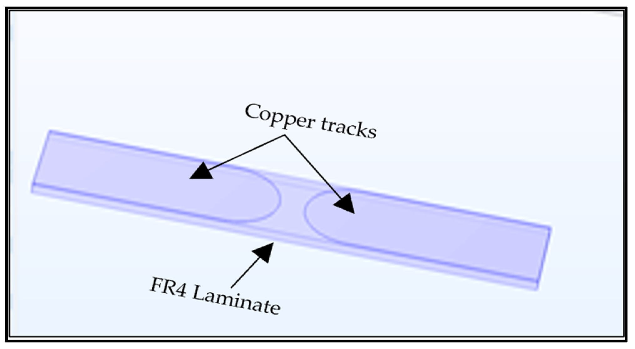
Figure 1.
Schematic representation of a PCB sample prepared on FR-4 laminate material with two conductive tracks with intermediate gaps, to create a quasi-uniform electrode arrangement.
Figure 1.
Schematic representation of a PCB sample prepared on FR-4 laminate material with two conductive tracks with intermediate gaps, to create a quasi-uniform electrode arrangement.
Figure 2.
Specimens of the PCBs with two copper tracks spaced at different distances: (a) Gap of 3 mm; (b) Gap of 5 mm; (c) Gap of 5 mm with a slit of 4 mm wide and 1 mm in length; (d) Gap of 10 mm; (e) A sample of PCB with 3 mm gap between conductive tracks encapsulated in dielectric gel.
Figure 2.
Specimens of the PCBs with two copper tracks spaced at different distances: (a) Gap of 3 mm; (b) Gap of 5 mm; (c) Gap of 5 mm with a slit of 4 mm wide and 1 mm in length; (d) Gap of 10 mm; (e) A sample of PCB with 3 mm gap between conductive tracks encapsulated in dielectric gel.
Figure 3.
The setup used for generating and applying high voltage to the test samples and measuring PD arrangement: (a) Schematic; (b) Pictorial description.
Figure 3.
The setup used for generating and applying high voltage to the test samples and measuring PD arrangement: (a) Schematic; (b) Pictorial description.
Figure 4.
A pictorial description of test cell with the sample placed and electrically connected to the high voltage electrodes: (a) Test cell; (b) Sample connected to the high voltage electrodes.
Figure 4.
A pictorial description of test cell with the sample placed and electrically connected to the high voltage electrodes: (a) Test cell; (b) Sample connected to the high voltage electrodes.
Figure 5.
Simulation of electric displacement field (
) (or charges built-up over the surface area) at the 3 mm spacing between the tracks of chosen PCB sample: (a) 2D CAD model; (b) Displacement field () at 5 kV; (c) Displacement field () at 30 kV; (d) Displacement field () at 60 kV.
Figure 5.
Simulation of electric displacement field (
) (or charges built-up over the surface area) at the 3 mm spacing between the tracks of chosen PCB sample: (a) 2D CAD model; (b) Displacement field () at 5 kV; (c) Displacement field () at 30 kV; (d) Displacement field () at 60 kV.
Figure 6.
PRPD pattern of electrical discharges arising on the surface of virgin PCB samples at the space between conductive tracks: (a) Inception of discharges (Group 1); (b) Nearby failure (Group 1).
Figure 6.
PRPD pattern of electrical discharges arising on the surface of virgin PCB samples at the space between conductive tracks: (a) Inception of discharges (Group 1); (b) Nearby failure (Group 1).
Figure 7.
PRPD pattern of electrical discharges arising on the surface of virgin PCB samples at the space between conductive tracks: (a) Inception of discharges (Group 2); (b) Nearby failure.
Figure 7.
PRPD pattern of electrical discharges arising on the surface of virgin PCB samples at the space between conductive tracks: (a) Inception of discharges (Group 2); (b) Nearby failure.
Figure 8.
PRPD pattern of electrical discharges arising on the surface of virgin PCB samples at the space between conductive tracks: (a) PD failure (Group 1); (b) PD failure (Group 2).
Figure 8.
PRPD pattern of electrical discharges arising on the surface of virgin PCB samples at the space between conductive tracks: (a) PD failure (Group 1); (b) PD failure (Group 2).
Figure 9.
PRPD pattern of the encapsulated PCB samples of Group 3, conditioned in deionized water at 90 °C temperature: (a) Gap of 3 mm; (b) Gap of 5 mm; (c) Gap of 5 mm, with an intermediate slit of 4 mm × 1 mm; (d) Gap of 10 mm.
Figure 9.
PRPD pattern of the encapsulated PCB samples of Group 3, conditioned in deionized water at 90 °C temperature: (a) Gap of 3 mm; (b) Gap of 5 mm; (c) Gap of 5 mm, with an intermediate slit of 4 mm × 1 mm; (d) Gap of 10 mm.
Figure 10.
PRPD pattern of the electrical discharges arising between the tracks of chosen PCB samples, conditioned by immersing in deionized water at 90 °C temperature resulting in a nearby insulation failure: (a) Gap of 3 mm; (b) Gap of 5 mm, without any intermediate slit between the gaps; (c) Gap of 5 mm, with an intermediate slit of 4 mm × 1 mm in dimension; (d) 10 mm.
Figure 11.
PRPD pattern of the inception of electrical discharges arising between the tracks of chosen PCB samples, conditioned by immersing in deionized water at room temperature: (a) Gap of 3 mm; (b) Gap of 5 mm, without any intermediate slit between the gaps; (c) Gap of 5 mm, with an intermediate slit of 4 mm × 1 mm in dimension; (d) Gap of 10 mm.
Figure 12.
PRPD pattern of the electrical discharges arising on chosen PCB samples, aged in deionized water at room temperature, resulting in a near-by insulation failure: (a) Gap of 3 mm; (b) Gap of 5 mm, without any intermediate slit between the gaps; (c) Gap of 5 mm, with an intermediate slit of 4 mm × 1 mm in dimension; (d) Gap of 10 mm.
Figure 13.
PRPD pattern of the inception of electrical discharges arising between the tracks of chosen PCB samples, aged by immersing in seawater at room temperature for a specific duration: (a) Gap of 3 mm; (b) Gap of 5 mm, without any intermediate slit between the gaps; (c) Gap of 5 mm, with an intermediate slit of 4 mm × 1 mm in dimension; (d) Gap of 10 mm.
Figure 14.
PRPD pattern of the electrical discharges arising between the tracks of chosen PCB samples, conditioned by immersing in sea water at room temperature, eventually resulting in a nearby insulation failure: (a) Gap of 3 mm; (b) Gap of 5 mm, without any slit between the gaps; (c) Gap of 5 mm, with an intermediate slit of 4 mm × 1 mm in dimension; (d) Gap of 10 mm.
Figure 15.
Trend manifested by the apparent charges of electrical discharges arising on the surface of the PCB samples aged in deionized water at 90 °C, with respect to the track spacing: (a) PD measured; (b) Corresponding test voltage.
Figure 15.
Trend manifested by the apparent charges of electrical discharges arising on the surface of the PCB samples aged in deionized water at 90 °C, with respect to the track spacing: (a) PD measured; (b) Corresponding test voltage.
Figure 16.
Trend manifested by the apparent charges of electrical discharges arising on the surface of the PCB samples aged in deionized water at 25 °C, with respect to the track spacing: (a) PD measured; (b) Corresponding test voltage.
Figure 16.
Trend manifested by the apparent charges of electrical discharges arising on the surface of the PCB samples aged in deionized water at 25 °C, with respect to the track spacing: (a) PD measured; (b) Corresponding test voltage.
Figure 17.
Trend manifested by the apparent charges of electrical discharges arising on the surface of the PCB samples aged in seawater at 25 °C, with respect to the track spacing: (a) PD measured; (b) Corresponding test voltage.
Figure 17.
Trend manifested by the apparent charges of electrical discharges arising on the surface of the PCB samples aged in seawater at 25 °C, with respect to the track spacing: (a) PD measured; (b) Corresponding test voltage.
Table 1.
Test samples and their respective aging conditions adopted.
Table 1.
Test samples and their respective aging conditions adopted.
| Group | Test Samples | Gap between Tracks | Test Conditions |
|---|
| 1 | Virgin PCB 1 | 5 mm | Without gel encapsulation |
| 2 | Virgin PCB 2 | 5 mm | With gel encapsulation |
| 3 | | 3 mm | |
| PCB 3 | 5 mm | Deionized water at 90 °C |
| | 5 mm with 4 mm slit | |
| | 10 mm | |
| 4 | | 3 mm | |
| PCB 3 | 5 mm | Deionized water at |
| | 5 mm with 4 mm slit | room temperature (RT) |
| | 10 mm | |
| 5 | | 3 mm | |
| PCB 3 | 5 mm | Sea water in room |
| | 5 mm with 4 mm slit | temperature |
| | 10 mm | |
Table 2.
Charges simulated at the electrode curvature of the PCB sample with different spacings.
Table 2.
Charges simulated at the electrode curvature of the PCB sample with different spacings.
| Spacing between the Tracks | |
|---|
| Maximum Value Simulated at 5 kV | Maximum Value Simulated at 30 kV | Maximum Value Simulated at 60 kV |
|---|
| | C/mm2 | C/mm2 | C/mm2 |
|---|
| 3 mm | 192 | 1.15 | 2.3 |
| 5 mm | 151 | 908 | 1.89 |
| 10 mm | 110 | 662 | 1.32 |
Table 3.
Measurement of electrical discharges arising on the surface of virgin PCB samples.
Table 3.
Measurement of electrical discharges arising on the surface of virgin PCB samples.
| Test Condition | Spacing | Discharge Inception | Nearing Failure | Failure Due to Discharge |
|---|
| App. Charge | Voltage | App. Charge | Voltage | App. Charge | Voltage |
|---|
| mm | C | kV | C | kV | C | kV |
|---|
| 1 Air | 5 | | 26.94 | | 31.95 | | 32.23 |
| 2 Sil. oil | 5 | | 27.41 | | 40.6 | | 40.61 |
Table 4.
Measurement of discharges arising on PCB samples aged in deionized water at 90 °C.
Table 4.
Measurement of discharges arising on PCB samples aged in deionized water at 90 °C.
| Spacing | Discharge Inception | Nearing Failure | Failure Due to Discharge |
|---|
| App. Charge | Voltage | App. Charge | Voltage | App. Charge | Voltage |
|---|
| mm | C | kV | C | kV | C | kV |
|---|
| 3 | | 3.128 | | 23.15 | | 23.36 |
| 5 | | 3.579 | | 26.54 | | 26.89 |
| 5 (Slit) | | 13.03 | | 38.14 | | 38.51 |
| 10 | | 19.48 | | 32.16 | | 33.48 |
Table 5.
Measurement of discharges on PCB samples aged in deionized water at room temperature.
Table 5.
Measurement of discharges on PCB samples aged in deionized water at room temperature.
| Spacing | Discharge Inception | Nearing Failure | Failure Due to Discharge |
|---|
| App. Charge | Voltage | App. Charge | Voltage | App. Charge | Voltage |
|---|
| Mm | C | kV | C | kV | C | kV |
|---|
| 3 | | 28.72 | | 33.17 | | 33.24 |
| 5 | | 12.26 | | 43.93 | | 46.46 |
| 5 (slit) | | 19.02 | | 41.02 | | 43.36 |
| 10 | | 12.61 | | 59.36 | | 60.51 |
Table 6.
Measurement of discharges arising on PCB samples aged in seawater at room temperature.
Table 6.
Measurement of discharges arising on PCB samples aged in seawater at room temperature.
| Spacing | Discharge Inception | Nearing Failure | Failure Due to Discharge |
|---|
| App. Charge | Voltage | App. Charge | Voltage | App. Charge | Voltage |
|---|
| Mm | C | kV | C | kV | C | kV |
|---|
| 3 | | 4.177 | | 35.38 | | 36.65 |
| 5 | | 8.565 | | 38.93 | | 39.16 |
| 5 (Slit) | | 22.97 | | 47.93 | | 48.88 |
| 10 | | 6.117 | | 43.62 | | 43.72 |


 ,
, 


