Article

Simple Discrete Control of a Single-Phase Voltage Source Inverter in a UPS System for Low Switching Frequency

by
Zbigniew Rymarski
Department of Electronics, Electrical Engineering and Microelectronics, Faculty of Automatic Control, Electronics and Computer Science, Silesian University of Technology, Akademicka 16, 44-100 Gliwice, Poland
Energies 2023, 16(15), 5717; https://doi.org/10.3390/en16155717
Submission received: 27 June 2023 / Revised: 25 July 2023 / Accepted: 26 July 2023 / Published: 31 July 2023
(This article belongs to the Special Issue Control and Modeling of Power Converters and Inverters)

Abstract

:
Previous research has shown that the inverter output voltage distortions are higher for low switching frequencies, and it is impossible to increase the controller gains because it will cause oscillations of the output voltage. The main reason is the real frequency domain characteristic of the PWM modulator and measuring traces, which can be modelled as switching periods delays. The thesis of this paper is that by using the control system that takes care of these delays, it is possible to decrease output voltage distortions for the standard loads for relatively low switching frequencies (e.g., 12,800 Hz). The Luenberger observer was implemented in the multi-input-multi-output passivity-based control of the system with the delay, in order to predict the state variables of the inverter. It is shown that state variable prediction is unnecessary for high switching frequencies (e.g., 51,200 Hz). The theory, simulations and breadboard verification, using the inverter model controlled with the real-time interface MicroLabBox, are presented.

1. Introduction

The problem of controlling the voltage source inverter (VSI) is important in UPS systems. These systems should fill the requirements of the EN-62040-3 standard [1], in which the static and dynamic, linear and nonlinear loads are defined. To design such a control system, the inverter should be defined and modelled taking in care the properties of the output filter coil core [2,3,4]. Linear modelling in the operating point seems sufficient and is commonly used; however, there are many approaches (Section 2) to the nonlinearity of the inverter model [5,6,7]. Today, sophisticated control is only digital, so discrete models are required. It can be discretised from the continuous model or calculated as a discrete system from state equations [8]. The first parameter of the VSI is the capacitance CF and ESR (equivalent serial resistance) RCF of the output filter capacitor—typically MKP. The capacitance CF is tens of μF and it is possible to assign a nominal value as real, whereas ESR is negligible. The inductance LF of the output filter coil for a high-quality coil core (e.g., Sendust alloy powder [9]) can be assigned as equal to the nominal value. For a cheap coil core (iron powder [10]), the inductance LF should be measured. In both cases of coil cores, the serial resistance RLF, depending mainly on the power losses in the core, seriously increases with the increase in the magnetizing coil current and its frequency is equal to the switching frequency. The best solution is to measure this resistance. It should be summed with the other serial resistances. Switched-on bridge transistors have a resistance from 50 to 200 mΩ per transistor. Two are always conducting, and the resistance of the PCB traces and connectors is present. Altogether, the sum of serial resistances is called in the paper “equivalent serial resistance” RLFe. The method for calculating the parameters of the VSI from its measured Bode plots enables the creation of the VSI model in the operating point [11,12,13]. The PWM modulator introduces one switching period delay. The feedback loop has galvanic isolation in all the voltage and current channels (the isolated amplifier in the output voltage channel, and transducers in the output and inductor channels), difference amplifiers, antialiasing filters, and analogue-to-digital converters. As it can be easily proved, the feedback loop operates efficiently (decreases the VSI output impedance) below the resonant frequency of the output filter [14]. This frequency is usually about 1 kHz. In this frequency range, the Bode plots of the feedback loop have been measured and successfully modelled in experimental models as the delay [15]. The PWM modulator and measuring trace can be modelled as a delay of two to three switching periods. The main thesis of this paper is that by using the control system that takes care of the delay, it is possible to decrease the output voltage distortions of standard loads for a low (≤12,800 Hz) switching frequency. The Luenberger observer [16,17,18,19] for the state variables for the multi-input-single-output control will be used. Section 2 presents the simple continuous model of the VSI. Section 3 describes the used modulation scheme for the three-level, double-edge PWM. Section 4 concerns the design of the output filter. Section 5 shows the method of discretizing the continuous model, while Section 6 presents the fully discrete model calculated directly from the state equations. Section 7 describes the identification of the VSI plant and the measuring traces of the VSI. Section 8 presents the theory of PBC control with the prediction of state variables and the simulations for different systems with a low switching frequency in control systems, with and without prediction. Section 9 presents MATLAB/Simulink simulations of the inverter. Section 10 shows breadboard verification. Section 11 presents the results of the simulation and the experimental verification. Section 12 is a discussion. Section 13 contains conclusions.
It is possible to assume that the equivalent serial resistance of the capacitor CF is RCF ≈ 0 (for parallel connected MKP metallized polyester capacitors in the experimental inverter, less than 10 mΩ). RLFe is the equivalent serial resistance of the whole inverter—the serial resistance of the filter coil LF, the switched-on transistors in the bridge and PCB traces. It was shown in [11,12,13] that RLFe is much higher than the DC resistance of the coil, depending on the switching frequency (fs = 1/Ts), the magnetizing coil current and, very strongly, on the coil core’s power losses. It was shown in [11,12,13] that the worst material is iron powder (e.g., Material Mix −26) and alloy powder (iron, silicon, aluminium); however, MS Sendust (previous name: Super MSS) is a very good material with a reasonable price [9,12].
K C T R L ( s ) = V O U T ( s ) V C T R L ( s ) = e s T s K I N V = e s T s V O U T ( s ) V F I N ( s ) = e s T s ω F 0 2 s 2 + 2 ξ F e ω F 0 s + ( 1 + R L F e R L O A D ) ω F 0 2 ,
where
ω F 0 = 1 L F C F ,   ξ F e = 1 2 ( R L F e C F L F + 1 R L O A D L F C F ) .
A modification of this simple model is the quasi-continuous transfer function [20,21] of the inverter (including RLOAD), which considers further ZOH discretization for the discrete control purpose (introducing the delay of half of Ts) and one Ts delay of the PWM modulator (3).
K C T R L ( s ) = exp ( s T s 2 ) exp ( s T s ) F L C ( s ) ( 1 s T s 2 ) 1 s T s 2 1 + s T s 2 ω F 0 2 s 2 + 2 ξ F ω F 0 s + ( 1 + R L F e R L O A D ) ω F 0 2
Modelling the load current as an independent disturbance or state variable has been the standard approach in inverter research for 40 years [22,23,24,25,26,27,28]. This allows the load impedance to be neglected in the state matrix. However, we are missing one feedback loop from the output voltage VOUT to the load current IOUT. After designing the control system, it is possible to check how the omission of this loop changes the real position of the poles of the closed-loop system (whether they do not go beyond the unit circle in the z plane). In [24] was shown how the omission of the load resistance shifts poles of the closed-loop system when using the Coefficient Diagram Method of the control [29,30,31].

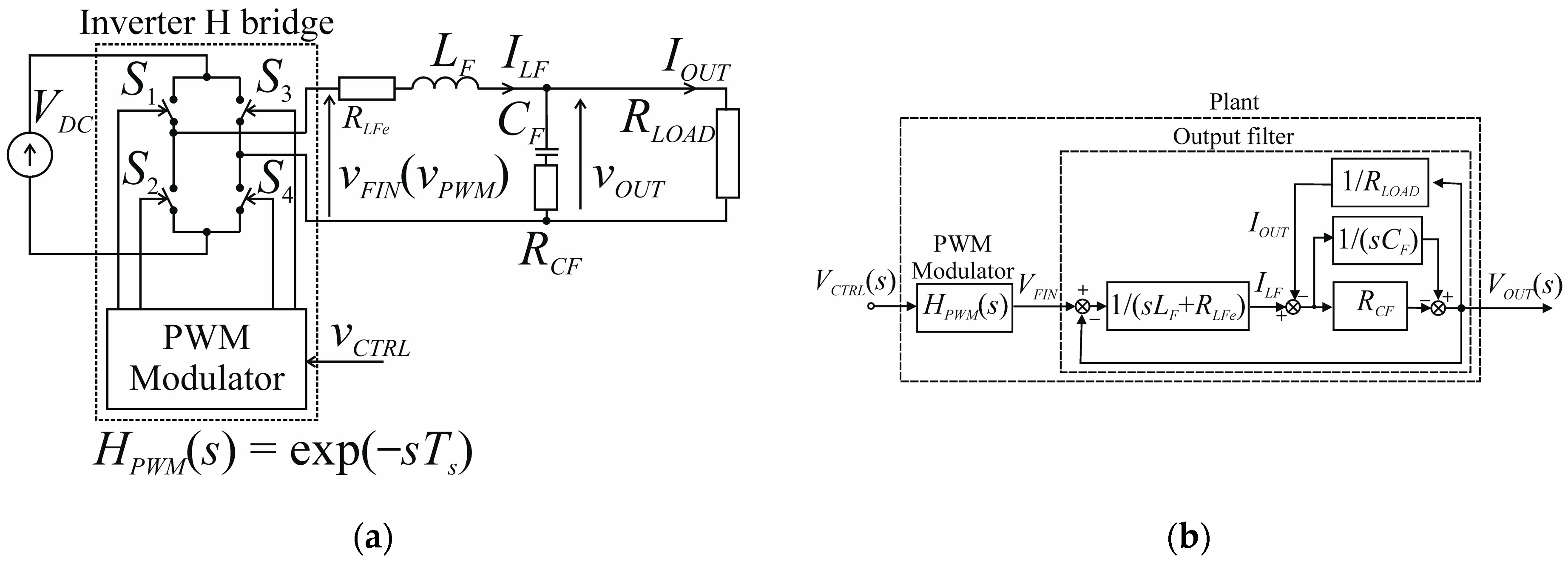
2. Continuous Model of the Voltage Source Inverter

Creating the VSI model and its mathematical description is the basic subject of the VSI control design. In [5], the calculation of the nonlinear characteristic of the coil in the LC output filter and its influence on the adaptive control loop were shown. Depending on the inductor core material, its inductance and the equivalent serial resistance varies with the amplitude and the frequency of the magnetizing current [2,3,4].
The influence of the nonlinear characteristic of the inductor in the inverter output filter on the design of the adaptive control loop (with the calculation of the nonlinear inductance characteristic) was presented in [5]. The change in the coil’s inductance and its equivalent serial resistance as a function of the amplitude and the frequency of its magnetizing current depends on the core material [2,3,4]. The change in inductance is small, 5%, for iron–silicon–aluminium alloy powder materials (e.g., Sendust (MS)/Super-MSS™ [9]). The equivalent serial resistance resulting from power losses in the core, in the core operating point for this core material, is 3–5 times lower than for a cheaper iron-powder material mix −26 [12]. So, the coil core material has an impact on the VSI model. The state–space equations of the VSI with pulse width modulation (PWM) can be solved, resulting in the nonlinear (exponential) dependency of state–space variables on the duty ratio of pulses [8]. In [6], the approximation by the Fourier series of the nonlinear control law was presented. Hammerstein’s approach (decomposition of the input–output relationship, where dynamics are represented by a linear transfer function and nonlinearities are represented through the identified black box) to the nonlinear modelling of VSI was presented in [7]. The nonlinear modelling of VSI is a bit more accurate than models with linear approximation of the inverter in the operation point; however, the linear theory results in quite acceptable accordance with the experimental VSI verification. The linear theory enables the simple design of the VSI controller.
The continuous linear model of the single-phase inverter is just the output LC filter and the discrete PWM modulator that can be modelled as a delay with the switching period Ts. The PWM modulator is a digital circuit (e.g., microprocessor) in which we store the duty ratio of the output pulse, and these data are on the output of the modulator in the next period.
The state vector is assigned as x = [ v O U T i L F i O U T ] T , the input vector (in the presented case, one variable) is u = v F I N and the output vector (in the presented case, one variable) is y = v O U T . The PWM modulator transfer function is H P W M = exp ( s T s ) .
The state matrix, input matrix and output matrix are (4).
A = 0 1 C F 1 C F 1 L F R L F e + R C F L F R C F L F 0 0 0 ,   B = 0 1 L F 0 ,   C = 1 0 0 .
The continuous time-invariant state–space equation is (5).
x ˙ = A x + B u
Finally, for RCF ≈ 0, the transfer function of the control voltage and the disturbance (the output current) is (6).
V O U T ( s ) = H P W M ω F 0 2 s 2 + s R L F e L F + ω F 0 2 V C T R L ( s ) ( s L F + R L F e ) ω F 0 2 s 2 + s R L F e L F + ω F 0 2 I O U T ( s )
The transfer control function of the VSI is (7).
K C T R L ( s ) = V O U T ( s ) V C T R L ( s ) = exp ( s T s ) K I N V = exp ( s T s ) V O U T ( s ) V F I N ( s ) = exp ( s T s ) ω F 0 2 s 2 + s R L F e L F + ω F 0 2
where the output impedance of the VSI with the open loop, that is, the disturbance transfer function, is (7).
Z O U T ( s ) = V O U T ( s ) I O U T ( s ) = ( s L F + R L F e ) ω F 0 2 s 2 + s R L F e L F + ω F 0 2

3. Modulation Scheme

The two-leg H bridge enables two or three levels of single-phase modulation. The three-level modulation results in a much lower level of harmonics than the two levels, in the sinusoidal modulated PWM waveform for the low modulation coefficient [32]. Each microprocessor that can be used to control VSI has the possibility of two-edge modulation that results in lower low-order harmonics than single-edge modulation. There are different modulation schemes—algorithms for driving the transistors in the H bridge in the three-level, two-edge single-phase modulation [32,33,34]. The best for control purposes is the first PWM scheme, in which it is possible to control the output waveform when it crosses the zero value. The transistors of a (two-leg) H-bridge (Figure 1a and Figure 2a) in the first modulation scheme (Figure 3), are switched with the frequency fs. The current flows through the serial connection of two switches on the diagonal of the bridge (S1 and S4 or S3 and S2, Figure 1a and Figure 2a) and the output PWM waveform, which has a double 2fs frequency is a coincidence of switching on two transistors. The control of the switches is described by Equations (9)–(12) and is presented in Figure 3. TON is the switching-on time. The double-output switching frequency enables one to design an output filter with the lower values of the filter parameters without increasing the switching frequency of transistors. For k = 1 to (fs/fm):
S 1 : T O N ( k ) / T s = 0.5 M sin ( k 2 π f s / f m ) + 0.5 M
S 2 : N O T ( S 1 )
S 3 : T O N ( k ) / T s = 0.5 M sin ( ( k 2 π f s / f m ) + π ) + 0.5 M
S 4 : N O T ( S 3 )

4. Design of the Output Filter

The VSI model was based on the output LFCF filter. The restriction of the output voltage ripple amplitude (13) 0.5VOUTripplepp of up to 3% determines the value of the product of LFCF (14). Calculating the quotient LF/CF is more ambiguous [8,32,35]. One of the solutions is creating the “cost function” Fcost (14) as a sum of absolute values of reactive power in the filter components [8,32,35,36,37]. However, the reactive power of an inductor is sometimes weighted two-times higher than that of the capacitor [36,37], because the reduced LF value decreases the VSI output impedance for the low frequency and improves the VSI dynamic properties. The presented design of the filter (17) is based on the minimization of the “cost function”, with the same weights for both absolute values of reactive powers of the inductor and capacitor [8,35,38]. The case of a single-phase, H-bridge, three-level inverter was presented. The LF and CF values depend on the load RLOAD and the switching frequency fs.
0.5 V O U T r i p p l e p p max 3 % V O U T h 1
From (13)
L F C F 1 f s
The cost function Fcost (15).
F cos t = ω m L F I L F h 1 R M S 2 + ω m C F V O U T h 1 R M S 2 = ω m L F I L F h 1 R M S 2 + ω m 1 f s L F V O U T h 1 R M S 2
F cos t L F = 0
The particular values of LF and CF from (14) and (16)
L F 1 f s R L O A D ,   C F 1 f s 1 R L O A D
Similar output filter calculations are the result of calculations presented in [39].
When the effective switching frequency of the VFIN is equal to 51,200 Hz (the double-switching frequency fs = 25,600 Hz of the bridge transistors, Figure 3), RLOAD = 50 Ω, the result from (17) is LF = 1 mH, CF = 0.4 μF; let us use CF = 1 μF. The feedback is always delayed by at least one switching frequency period Ts = 39 μs (fs = 25,600 Hz) in the digital PWM modulator. It is possible to assume that the inductor current is constant during one switching period and there is a resistive load. If the amplitude of the output current ILFmax is 5 A and the load is fully decreased in the maximum of output sinusoidal voltage, the increase in the output voltage will be ΔVOUT = TsILFmax/CF = 195 V. Such an instant increase in the output voltage is unacceptable (and saturates the control unit of VSI which can lead to further oscillations of the output voltage) and the CF value should be increased to 50 μF. In this case, the increase in the output voltage ΔVOUT = 4 V is acceptable. The presented values, about 1 mH and 50 μF, are typical for the low-output-power VSI.

5. Discretizing the Continuous Model of the VSI

Contemporary VSI is controlled using microprocessors or other digital devices (e.g., FPGA). The simplest approach is to discretize the continuous model of the inverter without delays KINV = VOUT(s)/VFIN(s). The approximation of the transformation s = (ln z)/Ts should be used. The bilinear transform (Tustin) s = (2/Ts)(z − 1)/(z + 1) gives the results most similar to the exact logarithmical transformation of the left half plane s into the unity circle in the plane z. The MATLAB c2d function with, e.g., the ‘Tustin’ discretization method can be used (18) and (19).
K I N V ( s ) = V O U T ( s ) V F I N ( s ) = t f ( [ ω F 0 2 ] , [ 1 2 ξ F e ω F 0 ω F 0 2 ] ) ;
K I N V c 2 d ( z ) = c 2 d ( K I N V , T s , t u s t i n ) ;
Finally, Equation (20) introduces the PWM modulator delay.
K C T R L c 2 d ( z ) = z 1 K I N V c 2 d ( z ) ;
All the discretisation methods introduce the delay (it was taken care of in model (3)). The disadvantage of this method is the same result for the single- or double-edged modulation, while the double-edged modulation introduces an additional delay (the voltage pulse TOFF time when the transistor is switched off depends on the previous pulse) and a lower THD.

6. The Discrete Model of the VSI

The discrete model of the VSI is created as a linearized solution of the state–space equation of the inverter for a particular method (e.g., single- or double-edged) of PWM [8,32,38,40]. For a multidimensional MIMO system with r inputs, n state variables and p outputs, using the solution of state equations for x ( t ) R n ,   u ( t ) R r ,   y ( t ) R p , initial variable conditions x(t0) and control conditions u(t0), where x = [vOUT iLF iOUT]T, u = vFIN, y = vOUT, it is possible to solve state–space Equation (5).
The general solution in one switching period for 0 ≤ tTs is (21).
x ( t ) = e A ( t t 0 ) x ( k T s ) + t 0 t e A ( t τ ) B u ( τ ) d τ
The solution of Equation (21) can be solved in the particular sectors of the switching period Ts for the double-edged PWM [32]. To linearize the solution of the equation the linear approximation (22) is used.
e A T O N k / 2 = I + A T O N k / 2 + A 2 T O N k 2 / 4 I + A T O N k / 2
Finally, the linearized state space equations are (23)–(25).
x ( ( k + 1 ) T s ) = e A T s x ( k T s ) + e A T s / 2 B V D C T O N ( k T s )
x k + 1 = A D x k + G D T O N k
y k = C D x k
The discrete state AD and control GD matrixes are (26)–(28).
A D = e A T s = Φ ( T s ) = L 1 [ ( s I A ) 1 ] t = T s
G D = e A T s / 2 B V D C = Φ ( T s / 2 ) B V D C
A D = Φ ( T s ) = ϕ 11 ϕ 12 ϕ 13 ϕ 21 ϕ 22 ϕ 23 ϕ 31 ϕ 32 ϕ 33 , G D = g 11 g 21 g 31 , C D = C
where
ξ F = 1 2 R L F e C F L F ;   ω F 0 = 1 L F L F ,
ϕ 11 = [ cos ω F 0 T s + ξ F sin ω F 0 T s ] exp ( ξ F ω F 0 T s ) ,
ϕ 12 = 1 ω F 0 C F sin ( ω F 0 T s ) exp ( ξ F ω F 0 T s ) ,
φ 13 = φ 12 + R L F e ( φ 11 1 ) ,
ϕ 21 = C F L F φ 12 ,
ϕ 22 = [ cos ( ω F 0 T s ) ξ F sin ( ω F 0 T s ) ] exp ( ξ F ω F 0 T s ) ,
ϕ 23 = 1 φ 11 ;   ϕ 31 = 0 ;   ϕ 32 = 0 ϕ 33 = 1 ,
g 11 = V D C ω F 0 sin ( ω F 0 T s / 2 ) exp ( ξ F ω F 0 T s / 2 ) ,
g 21 = V D C L F [ cos ( ω F 0 T s / 2 ) ξ F sin ( ω F 0 T s / 2 ) ] exp ( ξ F ω F 0 T s / 2 ) ,
g 31 = 0 .
The control transfer function and the output impedance of VSI can be expressed as (29)
V O U T ( z ) = z 1 g 11 + ( φ 12 g 21 φ 22 g 11 ) z 1 1 z ( φ 11 + φ 22 ) z 1 + ( φ 11 φ 22 φ 12 φ 21 ) z 2 T O N ( z ) + z 1 φ 13 + ( φ 12 φ 23 φ 13 φ 22 ) z 1 1 z ( φ 11 + φ 22 ) z 1 + ( φ 11 φ 22 φ 12 φ 21 ) z 2 I O ( z )
The delay with one Ts that exists in (29) is the feature of the double-edged modulation. The time between two consecutive pulses depends on the previous switching period control. For single-edged modulation, this delay is absent [32].
The gain of the VSI, with double-edged PWM and a digital modulator inserting a switching period delay Ts, is given by (30), (31):
K C T R L = V O U T ( z ) V C R T L ( z ) = z 1 K I N V = z 1 a 1 z 1 + a 2 z 2 1 + b 1 z 1 + b 2 z 2 ,
where
a 1 = T s V D C g 11 ;   a 2 = T s V D C ( φ 12 g 21 φ 22 g 11 ) ;   b 1 = ( φ 11 + φ 22 ) ;   b 2 = φ 11 φ 22 φ 12 φ 21 .
For high switching frequencies (e.g., 51,200 kHz), the difference between the discretized control transfer function and the discrete transfer function is low.

7. Measuring Bode Plots of the Inverter and Measuring Traces

To design the control of the VSI, its parameters should be known to define the VSI model. Additionally, Bode plots of the measuring traces should be appointed. The inverter bridge with the output filter can have parameters different from the nominal [11,12,13]. The parameter values depend mainly on the coil core material in the filter. For an iron powder core, the inductance LF seriously changes; for the Super MSS, it is almost constant. The power losses in the core cause an increase in the equivalent serial resistance RLFe. Inductance LF and the equivalent serial resistance RLFe should be measured in the chosen VSI operating point. The fundamental frequency fm = 50 Hz was set to be constant. Three switching frequencies were checked in the experimental VSI: fs = 12,800 Hz, 25,600 Hz or 51,200 Hz (the frequency of the voltage pulses on the coil in the presented PWM scheme is double 2fs, Figure 3). The DC supply voltage VDC, the load resistance RLOAD and the switching frequency fs were assigned for the selected operating point. The generated test signal VCTRL (Figure 4) was the sum of the fundamental harmonic and the excitation signal, that is, the n-th harmonic of the fundamental harmonic (32) [11,12,13].
For k = 1 to fs/fm
V C T R L ( k ) = r o u n d ( M · f l o o r 1 2 f C O M P f s ( A sin ( k 2 π f s / f m ) + ( 1 A ) sin ( n k 2 π f s / f m ) ) )
where M is the modulation depth (typically M = 0.9, to avoid distortions of the fundamental harmonic), fCOMP is the input frequency of the PWM unit comparator (in STM32F407VG microprocessor fCOMP = 84 MHz), A is the relative amplitude of the fundamental harmonic (A = 0.9–0.95) and k = 1…(fs/fm). The switching frequency fs is always a harmonic of the fundamental frequency fm = 50 Hz. The reference waveform is represented by fs/50 samples of the sinusoidal reference per the fundamental period Tm = 20 ms. The number of samples of the n-th harmonic—the excitation—is equal to fs/(n50) in one fundamental period. For the minimum number of ten samples per period of the generated harmonics, in the case of fs = 12,800 Hz: nmax = 25, fs = 25,600 Hz: nmax = 50 and fs = 51,200 Hz: nmax = 100. Finally, nmax = 100 was used for fs = 12,800, 25,600 and 51,200 Hz because it has a high attenuation over the 25th harmonics (for LF = 1 mH, CF = 51 μF, the output filter resonant frequency was 705 Hz, below the 25th harmonic) and the error in the measurement of the harmonics close to the 100th harmonic is not practically important. The MKP-type VSI output capacitor CF = 51 μF was the same as in the experimental inverter. The accuracy of appointing the maximum gain is better for the lower-frequency step grid [13]. For lower damping, the frequency step grid should possibly be lower; for high damping, finding the maximum on the Bode plot will be always inaccurate. For the calculation of the LF and RLFe parameters, the maximum value of the damping coefficient should be ξF2 < (1 + RLFe/RLOAD)/2 for RLOAD >> RLFe. The amplitude of the measured fundamental harmonic should be initially adjusted to 50–75% of the ADC range (the used 13-bit bipolar analogue-to-digital converter ADC has a range of −4095 to 4095; the required amplitude of the fundamental harmonic should be 2000–3000 units). The complex test signal vCTRL (35) is generated in the DAC/ADC units from −floor(0.5fCOMP/fs) to floor(0.5fCOMP/fs). It should be checked that for a complex test signal with an excitation component frequency near the VSI filter resonant frequency, the measured value is inside the range of ADC. The amplitude of excitation |hnIN| = 1 − A should have a value of 5 to 10%. It was shown [41] that the lowest comparator frequency is fCOMP = 68 MHz for fs = 25,600 Hz and the double-edged PWM modulation, for which there were no additional distortions caused by the insufficient resolution of the generated waveform (in STM32F407VG, there is fCOMP = 84 MHz). The main assumption is that the fundamental harmonic is not attenuated in the inverter and it is delayed as all the components of the test signal (the Ts delay in the PWM modulator is not present in the relative calculations because it concerns the whole signal).
The values of the input and output excitations are compared, respectively, with the fundamental harmonic in the input and output. Such a solution solves the problem of the different units in the VSI output (volts) and PWM modulator input test signal (in ADC units). The amplitudes and phases of the excitation harmonic components (33) of the input and output complex signals are calculated using the fft transform [14].
For n = 1…nmax
K I N V ( j 2 π f n ) = = V O U T ( n f m ) / V O U T ( f m ) V C T R L ( n f n ) / V C T R L ( f m ) exp ( j { [ arg ( V O U T ( n f m ) ) arg ( V O U T ( f m ) ) ] [ arg ( V C T R L ( n f m ) ) arg ( V C T R L ( f m ) ) ] } )
The magnitude Bode plot is (34)
K I N V ( n f n ) = 20 log V O U T ( n f m ) / V O U T ( f m ) V C T R L ( n f n ) / V C T R L ( f m )
The phase Bode plot is (35)
arg ( n f m ) = [ arg ( V O U T ( n f m ) ) arg ( V O U T ( f m ) ) ] [ arg ( V C T R L ( n f m ) ) arg ( V C T R L ( f m ) ) ]
The switching frequency fs and the load RLOAD are parameters which should be kept constant during one measurement series. The measured row data series—magnitudes and phases of the inverter together with the measurement trace—are sent to PC where the previously measured magnitudes (dB) and phases (degrees) of the measurement trace are subtracted from the corresponding row data. From the magnitude Bode plot, the damping coefficient ζF (36), the inductance LF (37) and the serial equivalent resistance RLFe (38) can be calculated [14] for the assumption RLOAD >> RLFe.
ξ F 1 2 [ 1 ( 1 1 | K I N V | max 2 ) ]
L F = 1 2 ξ F 2 ω max 2 C F ,   for   ξ F 2 < 0.5
R L F e = ( 2 ξ F ω max 2 1 2 ξ F 2 1 R L O A D C F ) 1 2 ξ F 2 ω max 2 C F   for   R L O A D > 1 2 ξ F 2 2 ξ F ω max C F   and   ξ F 2 < 0.5
The error (41) in the calculation of the damping coefficient ξF was caused by the Δωmax error of appointing ωmax (39), (40).
ω max 2 = ( 1 2 ξ F 2 ) ω F 0 2
Δ ξ F = ξ F ω max Δ ω max = 1 2 ω F 0 2 ω max ω F 0 2 ω max 2 Δ ω max
Δ ξ F = 1 2 1 2 ξ F 2 ξ F Δ ω max ω max
The measured serial equivalent inductance error is low, and approximately can be assigned ΔLF ≈ 0 (43) because the component errors cancel each other out (42).
Δ L F = L F ξ F e Δ ξ F + L F ω max Δ ω max = 4 ξ F ω max 2 C F Δ ξ F 2 1 2 ξ F 2 ω max 3 C F Δ ω max
Δ L F 0
The error of the serial equivalent resistance RLFe (45) depends on the damping coefficient ξF and Δωmax that is equal to 0.5 frequency grid.
Δ R L F e = R L F e ξ F Δ ξ F + R F e L F Δ L F 2 L F C F Δ ξ F
Δ R L F e = L F C F 1 2 ξ F 2 ξ F Δ ω max ω max
Figure 5 presents the error of RLFe as a function of the damping coefficient ξF and frequency resolution Δfmax. This error ΔRLFe (for LF = 1 mH, CF = 51 μF) is serious, up to 1.5 Ω, for the low damping coefficient, which is the case of a low resolution for Δfmax = 50 Hz (frequency step grid 100 Hz). The full real value of RLFe is 1 to 2 Ω for the 1 mH coil DC resistance of about 0.2 Ω, the MOSFET bridge transistors with RDS = 0.2 Ω (there are always two serially connected transistors conducting), and the coil core made of Sendust magnetic material [9] with a low power loss. So, ΔRLFe = 1.5 Ω is unacceptable and the frequency step grid should be decreased.
Figure 6 presents the Bode plots of two experimental inverters. It can be noticed that in both cases, these frequency domain characteristics can be approximated in the frequency range up to the corner frequency of the output filter (for LF = 1 mH, CF = 51 μF, it is 705 Hz) as the simple delay with two switching periods Ts. This approximation (46) of the measuring trace transfer function for f < 1000 Hz will be used in the simulations.
K T R A C E ( s ) e s 2 T s   for ω   <   2 π 1000   [ 1 / s ]

8. The Prediction of the State Variables

It was shown that the transfer function of the measurement trace and the PWM modulator can be approximated with a simple delay (2Ts is the measuring trace and Ts is the PWM modulator). For the high switching frequency (51,200 Hz and more) this delay is not so important for the design of the control loop [42]. For the lower switching frequency, one of the solutions can be the prediction of the state variable at the next sampling instant [43]. The full-order state Luenberger observer [18,19] will be used. It is quite convenient because we do not need to know exactly the transfer function of the measurement traces.
The discrete state space equations for state variables x = [ v O U T i L F i O U T ] T and output variable y(k) = vOUT(k) were described in (26), (27). The predicted state variables at the next sampling instant are (47).
x ^ ( k + 1 ) = A D x ^ ( k ) + G D T O N ( k ) + L [ y ( k ) C D x ^ ( k ) ]
L is discretized observer gain matrix.
The error system is obtained from (48):
e ( k + 1 ) = ( A D L C D ) [ x ( k ) x ^ ( k ) ] = ( A D L C D ) e ( k ) ,
For three state variables:
L = [ l 1 l 2 l 3 ] T
The characteristic equation of the observer is (49).
det ( z 1 A D + L C D ) = 0
According to the principle of separation of estimation and pole placement of the “separation theorem”, the roots of the characteristic equation of the observer (49) are independent of the closed-feedback-loop control system. However, the observer eigenvalues should enable a faster convergence to zero of the observation error than that of other transient processes in a closed-loop system. Better observer dynamics are obtained if the roots of their characteristic Equation (49) are closer to zero on the z-plane (their absolute value is lower) than the roots of the characteristic equation without estimation det ( z 1 A D ) = 0 . E.g., in [44], the observer poles are selected to be about 0.8 times closer to the origin than the open-loop poles at the same phase angle. In [45], the Luenberger observer was designed with its dynamics three times faster than the fastest pole of the plant.
The characteristic equation of the open-loop system with the estimation is (50), (51).
det z φ 11 + l 1 φ 12 φ 13 φ 21 + l 2 z φ 22 φ 23 0 + l 3 0 z 1 = 0
1 + z 1 [ 1 φ 11 φ 22 + l 1 ] + z 2 [ φ 22 + φ 11 + φ 11 φ 22 - φ 12 φ 21 ( 1 + φ 22 ) l 1 + φ 12 l 2 + φ 13 l 3 ] z 3 [ φ 11 φ 22 + φ 12 φ 21 + l 1 φ 22 - φ 12 l 2 + ( φ 12 φ 23 φ 13 φ 22 ) l 3 ] = 0
Manabe presented the coefficient diagram method (CDM) [29,30,31] to design a controller where coefficients of the closed-loop characteristic equation are calculated from the Manabe standard form. They depend on the time constant τ of the closed-loop system. Relation (52) is the discretized characteristic equation of the closed-loop system.
P ( z 1 ) = i = 0 n p z i ( τ / T s ) z i
The experimental work [20] showed that for the values of LF = 1 mH, CF = 51 μF, and a switching frequency of fs = 12,800 to 51,200 Hz, the best results of control were for τ/Ts = 5 to 8. So, let us assign pzi(τ/Ts) for the lower τ/Ts for the characteristic equation of the observer, which fills the requirement that the observer should be faster than the closed-loop system (the further adjustment—individual decreasing gains from τ/Ts = 1, leads to gains of observer τ/Ts equal to about 7 to avoid system oscillations). Equation (53) should be solved to obtain the gains li of the observer for the assigned τ/Ts.
1 0 0 1 φ 22 φ 12 φ 13 φ 22 - φ 12 φ 12 φ 23 φ 13 φ 22 l 1 l 2 l 3 = p z 1 + 1 + φ 11 + φ 22 p z 2 φ 22 φ 11 φ 11 φ 22 + φ 12 φ 21 p z 3 + φ 11 φ 22 φ 12 φ 21
Table 1 presents the gains of the observer in the absolute values of the roots of its characteristic equation for the low switching frequency fs = 12,800 Hz and relative time constants τ/Ts from 1 to 6. The roots of the characteristic equation of the observer for the lower τ/Ts are closer to zero for the z-plane in Manabe CDM. This research concerns the comparison of operating at a low switching frequency fs = 12,800 Hz and operating at a high switching frequency fs = 51,200 Hz, because of the higher values of the switching frequency when the prediction is not necessary (the delay in the inverter system is low).
In [10,20,42,46] the passivity-based control for the voltage source inverters was presented. When the supplied energy in a system exceeds the stored energy, the system is passive. The passive system is stable—this is the idea of PBC. The energy in an inverter is stored in the components of the output filter—the filter coil and the filter capacitor–and can be described by the Hamiltonian function (54) H(x) (sometimes H(x) is called a Lyapunov function [47]).
H ( x ) = 1 2 ( L F i L F 2 + C F v O U T 2 )
The discrete control law of PBC for the predicted values of state variables is (55), (56), from [42].
v ^ C T R L ( k + 1 ) = R i i ^ L F ( k + 1 ) + ( R i + R L F ) i ^ L F r e f ( k + 1 ) + L F i ^ L F r e f ( k + 1 ) i ^ L F r e f ( k ) T c + v O U T r e f ( k + 1 )
i ^ L F r e f ( k + 1 ) = K v [ v O U T r e f ( k + 1 ) v ^ O U T ( k + 1 ) ] + C F v O U T r e f ( k + 1 ) v O U T r e f ( k ) T c + i ^ O U T ( k + 1 )
where:
v ^ O U T ( k + 1 ) = φ 11 v O U T ( k ) + φ 12 i L F ( k ) + φ 13 i O U T ( k ) + g 11 v ^ C T R L ( k ) V D C T s + l 1 [ v O U T ( k ) v ^ O U T ( k ) ]
i ^ L F ( k + 1 ) = φ 21 v O U T ( k ) + φ 22 i L F ( k ) + φ 23 i O U T ( k ) + g 12 v ^ C T R L ( k ) V D C T s + l 2 [ v O U T ( k ) v ^ O U T ( k ) ]
i ^ O U T ( k + 1 ) = i O U T ( k ) + l 3 [ v O U T ( k ) v ^ O U T ( k ) ]
The state–space Equations (57)–(59) are different from (47) because predicted space variables are not directly used in the equations. Using the predicted variables (47) is the typical approach [48]. But our CD = [1 0 0], and the output variable is dependent only on the output voltage. So, the measured values of the variables were used directly in (57)–(59) because there was no other way of implementing them in the prediction procedure.
The important problem in PBC is the choice of the current gain Ri and the voltage gain Kv. It was shown in [14,26,47] that the bottom limits of gains are RLFe + Ri > 0 and Kv > 0. The upper limits of Ri and Kv gains are a result of the limitation of the control voltage vCTRL possible speed. The higher values of the gains cause saturation of the PWM modulator but do not always cause oscillations. Sometimes, slightly increasing the gains over these limits can decrease the distortions of the output voltage for the nonlinear load. But it should be remembered that during saturation, the feedback loop does not work. The derivative of the control voltage in one switching cycle should be lower than the maximum increase in the output PWM signal that is equal to VDC/Ts.
We can assume that d(vOUTref)/dt ≈ 0 in one sampling period. The control law without prediction is (60) and (61):
v C T R L ( k T s ) = R i i L F ( k T s ) + ( R i + R L F e ) i L F r e f ( k T s ) + L F d i L F r e f ( k T s ) d t + v O U T r e f ( k T s )
i L F r e f ( k T s ) = K v [ v O U T r e f ( k T s ) v O U T ( k T s ) ] + C F d v O U T r e f ( k T s ) d t + i O U T ( k T s )
From (61) for the resistive load RLOAD:
i L F r e f ( k T s ) K v v O U T r e f ( k T s ) + ( 1 R L O A D K v ) v O U T ( k T s )
Let us assume the operation with the load RLOAD = ∞.
d i L F r e f ( k T s ) d t K v d v O U T ( k T s ) d t
The absolute value of the derivative of vCTRL for the load RLOAD = ∞ is (64).
d v C T R L ( k T s ) d t K v L F d 2 v O U T ( k T s ) d t 2 + K v ( R i + R L F e ) d v O U T ( k T s ) d t + R i d i L F ( k T s ) d t
In one switching cycle
d i L F ( k T s ) d t max , min ± V D C L F ,   d v O U T ( k T s ) d t max i L F C F ,   d 2 v O U T ( k T s ) d t 2 max d d t ( i L F C F ) max ± V D C L F C F
Finally, the absolute value of the derivative of vCTRL for the load RLOAD = ∞ is (66).
d v C T R L ( k T s ) d t max K v [ L F + ( R i + R L F e ) T s ] V D C L F C F + R i V D C L F
The upper limits of Ri and Kv gains are (67).
K v [ L F + ( R i + R L F e ) T s ] 1 L F C F + R i L F < f s
Figure 7a,b presents the graphic visualisation of Equation (67), adequately for fs = 12,800 and 51,200 Hz, while omitting the delays. When the left side of this equation is lower than the switching frequency, the gains are in the allowable range. The curves of equality of the left side of Equation (67) and the switching frequency—the border values of gains—are presented in Figure 7c for fs = 12,800 and 51,200 Hz. Taking values of the Ri and Kv gains from these curves below them, we can be sure that there will be no oscillations in the output voltage. However, it is possible to check experimentally higher values of the gains to decrease the error of the control. The presented values of gains are valid for Simulink simulation because we do not need to scale the voltage and currents. We only divide all the measured variables by the VDC that is on the input of the inverter because the input of the modulator is inside +1/−1. The other problem is the modulation index. The lower this index, the higher the dynamics of the modulator. However, in real inverters, the modulation index should be close to unity. Equation (67) does not consider the modulation index M value because the maximum carrier-slope increase does not depend on M. Equation (67) is calculated for RLOAD = ∞, the worst case being that the restrictions of the Kv value for the existing load resistance will be slightly lower. The higher value of the gains, the lower the output voltage error and the lower the THD coefficient. That is why it is possible to obtain much lower THD for higher switching frequencies.

9. Simulation of the Inverter with the Delay in the Measurement Traces

Figure 8 presents the output voltage waveform of the open-loop inverter with the nonlinear rectifier load R = 100 Ω and C = 430 μF.
Figure 9a presents the simulation model without the delays in the measuring traces for the low switching frequency fs = 12,800 Hz. Figure 9b,c presents the output voltage, output current and the control voltage waveforms for LF = 1 mH, RLFe = 1 Ω, CF = 51 μF, fs = 12,800 Hz, the nonlinear rectifier load R = 100 Ω and C = 430 μF, the modulation index M = 0.7, and the PBC control (60) and (61) without prediction. In Figure 9b, Kv = 0.3, and Ri = 4 from the border line from Figure 7b (THD = 2.69%). However, it is possible to increase the gains Kv = 0.5, Ri = 25 (Figure 9c) whilst accepting some oscillations of the control voltage, in order to decrease distortions (THD = 1.04%). In the simulated measurement traces (Figure 8a) there are only ZOH modules simulating the analogue-to-digital converters (ADCs).
In Figure 10a, the 2Ts delays in each of the measuring traces were added to make the simulation model more similar to the experimental model (Figure 6c,d) for fs = 12,800 Hz. The gains Kv and Ri of PBC were reduced from the border values Kv = 0.3 and Ri = 4 (Figure 10b) to 0.1 and 4 (Figure 10c) to decrease the output voltage oscillations. The controller architecture was the same as in Figure 9a. The controller works wrongly because the output voltage distortions are higher than in the open-loop inverter (Figure 8), which is ridiculous.
As shown in Figure 11a, the inputs of the PBC controller (55), (56) were predicted (57)–(59). The gains of the observer l1, l2, l3 were initially calculated for τ/Ts = 1 (Table 1) and then reduced to 0.285, −0.778 and −0.092 (the highest values for which there were no oscillations of the output voltage for the particular gains) and the gains Kv and Ri were adjusted to 0.1 and 4. In all the cases, the coefficient of the control quality was the THD of the output voltage.
To show the influence of delays in the measurement traces (depending on the switching frequency) for the higher switching frequency (51,200 Hz), Figure 12 presents the results of the simulation of the inverter with delays of 2Ts in the measuring traces and the PBC controller, without prediction, for fs = 51,200 Hz. It can be seen that the THD is very low (0.87%), and there is no need to use the observer. Let us compare the shape of the output current waveforms from Figure 11b and Figure 12. The current in Figure 12 is forced to increase immediately even if there are 2Ts delays, owing to possible higher controller gains. Table 2 presents the results (THD) of the control in simulations.

10. The Experimental Verification of Output Voltage Distortions

Real-time interface (RTI1202 with FPGA—MicroLabBox) with MATLAB 2021b (with the dSpace RTI Electric Motor Control Blockset libraries) is the best choice for experimental verification of the previous SIMULINK simulations [46]. The main trouble of the microprocessor-based (or FPGA-based) control is scaling the measurement trace gain. In the case of the RTI, all the signals can be displayed on a PC monitor using ControlDesk 7.5 (dSpace 2021b) software, and the gains in the Simulink blocks can be adjusted. All the output voltage, output current and inductor current waveform amplitudes (for the modulation coefficient M = 1, the specified sinusoidal output voltage amplitude and the chosen load resistor) should be equal to the specified value 0.5 because the reference output voltage waveform is 0.5 sin (2π50t). The range of the input values of the PWM block was equal to 0–1. Two sinusoidal waveforms shifted mutually 180 degrees in the phase, with the zero level shifted by 0.5 and a maximum amplitude of 0.5 as the inputs of the PWM block to realize the PWM scheme from Figure 3. For a modulation index of M = 0.7, the output voltage scaling gain was −1.5 (it should be reversed), and the output and inductor currents have gains of 2.7. The measured signals were shifted by small constant values to adjust their zero-crossing level. The next step was to divide the current measurements by the load resistance (for the nominal load, scaling was 50 Ω). Experimental verification using RTI is sufficient; however, a further design step is to create software for the microprocessor. This is the reason why the architecture of the RTI1202 software is based on interrupts from the PWM unit, like in the microprocessor. The trigger line 1 events from an EMC multichannel PWM block are handled by an ADC class 1 hardware interrupt block (HWINT), connected to the input port of a function-call subsystem (Figure 13a). The function-call subsystem (Figure 13b) contains all the components of the inverter control loop, such as the EMC multichannel PWM block, the ADC class 1 block and the PBC controller, with amplifiers of all the measured signals. The sample time of all the blocks is inherited from the PWM block triggering event (it can be set only in this block). The experimental inverter bridge transistors are driven with four DIO class 1 3.3 V digital outputs: a noninverted channel 1 (corresponds to S1 from Figure 2) and channel 2 (S3 in Figure 2), and an inverted channel 3 (S2 in Figure 2) and channel 4 (S4). The dead time between switching off and on two transistors in the same leg of the bridge is equal to 500 ns for the Si-MOSFET transistors (IRFP360) and is implemented in IR2184-integrated circuits in the experimental inverter. The output voltage, output current and inductor current are measured via ADC Class 1 channel 1, with a single conversion (−10–+10 V input range) after the trigger event from the PWM block.
Figure 14 presents the same waveforms from the experimental inverter as Figure 8 and Figure 10, Figure 11 and Figure 12 for simulation. The gains and the distortions (THD) of the output signal are presented in Table 3. Figure 15 presents the tested experimental inverter with MicroLabBox (rti1202).

11. Results

Comparing Table 2 and Table 3, it can be seen that the distortions are 1 to 2% higher in the experimental verification than in the simulations. The reason could be the ripple output voltage in the experimental VSI. The controller gains in the simulations and the experimental inverter were adjusted from the initial values from the border lines in Figure 7c to obtain the lowest THD of the VSI output voltage without oscillations. However, in both cases of the simulation and the experimental verification, it was shown that for the low switching frequency (12,800 Hz), a lack of prediction in the control system can cause higher distortions of the output voltage than in the case of the open loop. For the high switching frequency (51,200 Hz), no prediction is required. Similar results in simulations and experimental verification prove that the approximation of the measuring trace Bode plots in the bandpass 0–1000 Hz, with delays equal to 2Ts, is appropriate.

12. Discussion

The simulations and the breadboard verification showed that the measurement traces can be modelled as the delay with some switching periods and even using the MISO control (e.g., PBC) is insufficient for a low switching frequency (about 10 kHz). However, this control is perfect for a high switching frequency (about 50 kHz). For a low switching frequency, the delay in the measurement traces causes oscillations of the output voltage even for the low gains of the controller (below the border curve in Figure 7c, because the reason for these oscillations is not considered there). The distortions of the output voltage can be higher than without any instantaneous control. The high switching frequency allows for an increase in the controller gains and decreases the output voltage distortions. Using the prediction of the state variables is the solution for a low switching frequency, e.g., using the state equations with the Luenberger observer. In this way, calculations of the variables are more flexible for the different delays in the measurement traces. The whole time, the theoretical discrete model of the inverter was used. The gains of the Luenberger observer are initially calculated using the coefficient diagram method for the different delays of the closed-loop observer. Initially, one switching period delay of the observer was taken into the calculation of the initial gains and then the gains of the observer were experimentally decreased to obtain the lowest-output voltage distortions. Finally, the adjusted observer dynamics were comparable with the gains of the observer with about seven switching period delays. It can be concluded that for a low switching frequency (about 10 kHz) the observer is necessary because of delays in the measuring traces. The best results can be obtained without the prediction for a high switching frequency (about 50 kHz). The observer is the additional subsystem of the control loop and should be treated as a necessary evil, because it can cause some instability. The gains of the PBC controller were adjusted to the lowest distortions of the output voltage. In some cases, it was able to increase gains over the borderline of gains from Figure 7c and to accept small oscillations in the control voltage. Further increases in the controller gains increase the output voltage distortions.

13. Conclusions

Most of the measuring traces in the inverters have Bode plots that, in the range up to the corner frequency of the output filter, can be modelled as a delay equal to some switching periods. The only possibility for the low-output voltage distortion operation of a MISO instantaneous control loop with a low switching frequency (e.g., 10 kHz), in a real device with delays in the measuring traces, is to use an observer, e.g., the simple Luenberger type. The work with a high switching frequency (e.g., 50 kHz) makes this prediction unnecessary, because the delay in the measuring traces usually depends on the switching frequency, and the prediction unnecessarily complicates the control loop, even increasing the distortions.

Funding

The author was supported by a pro-quality grant from the Rector of the Silesian University of Technology, Zbigniew Rymarski, grant number: 02/140/RGJ23/0026. This research was partially supported by the Polish Ministry of Education and Science funding for statutory activities (BK-236/RAU11/2023).

Data Availability Statement

All data files with results of simulations and measurements, the software for VSI simulation and control the experimental inverter are in the private possession of the author.

Acknowledgments

The author would like to thank Andrzej Tutaj, of Technika Obliczeniowa sp. z o. o. (www.tobl.com.pl) (accessed on 25 July 2023) for his support in the utilization of MicroLabBox, and Krzysztof Bernacki, Department of Electronics, Electrical Engineering and Microelectronics, Faculty of Automatic Control, Electronics and Computer Science, Silesian University of Technology, Gliwice, Poland, for his previous cooperation in inverter control research and his participation in the power electronics laboratory creation.

Conflicts of Interest

The author declares no conflict of interest.

Abbreviations

VSIVoltage Source Inverter;
THDTotal Harmonic Distortion;
CDMCoefficient Diagram Method;
PBCPassivity-Based Control;
ESREquivalent Series Resistance of the capacitor.
The inverter parameters symbols:
CFThe output filter capacitor or capacitance (Figure 1 and Figure 2);
LFThe output filter coil or inductance (Figure 1 and Figure 2);
RCFThe series resistance of the output capacitor (ESR), assigned equal to 0;
RLFeThe equivalent serial resistance of the whole inverter, the sum of the serial resistance of the filter coil LF, the resistances of two (on the diagonal of the inverter bridge) switched-on transistors in the bridge and the resistance of the PCB traces, connections, etc., strongly depends on the power losses in the output filter coil core;
fsThe switching frequency;
fmThe fundamental frequency (50 Hz);
ωF0The angular resonant frequency of the output filter;
ωmaxThe angular frequency, for which the magnitude Bode plot has the maximum;
TsThe switching period;
TONThe switching-on time.
The load parameters symbols:
RLOADThe load resistance (Figure 1) for the pure resistive load;
R, Cthe resistance and the capacitance of the nonlinear rectifier RC load (according to EN-62040-3 for PF = 0.7).
The currents and voltages symbols:
ILF, iLFThe filter coil (inductor) current (Figure 1 and Figure 2);
ILFh1RMSThe RMS value of the fundamental harmonic of the inductor current;
IOUT, iOUTThe inverter output current (Figure 1 and Figure 2);
VDCThe DC voltage supplying the inverter (Figure 1 and Figure 2);
VCTRL, vCTRLThe input voltage of the PWM modulator—the control voltage (Figure 1 and Figure 2);
VOUT, vOUTThe output voltage of the inverter (Figure 1 and Figure 2);
VOUTh1The amplitude of the fundamental harmonic (the first harmonic) of the inverter output voltage;
VOUTh1RMSThe RMS value of the fundamental harmonic of the inverter output voltage;
VOUTrippleppThe peak-to-peak value of the output ripple voltage;
VPWM, vPWMThe square output voltage waveform of the inverter bridge, the input voltage of the filter;
VFIN, vFINThe envelope of the inverter bridge input voltage VPWM used in calculations—delayed to vCTRL with Ts.
The transfer functions symbols:
K C T R L ( s ) = V O U T ( s ) V C T R L ( s ) The transfer function of the control signal of the inverter with the PWM modulator;
K C T R L c 2 d ( z ) The discretized transfer function of the inverter with the PWM modulator;
K I N V = V O U T ( s ) V F I N ( s ) The transfer function of the bridge with the output filter without the PWM modulator;
KAMPThe transfer function of the measuring trace;
FLC(s)Transfer function of the output filter, equal to KINV(s);
ZOUT(s)output impedance of the inverter.
The state variables and matrixes symbols:
A, B and CThe state matrix, input matrix and output matrix of the inverter, respectively;
x = [ v O U T i L F i O U T ] T The inverter state variables vector;
x ^ = [ v ^ O U T i ^ L F i ^ O U T ] T The predicted state variables vector;
u = v F I N The inverter input vector (in the presented case one variable);
y = v O U T The inverter output vector (in the presented case one variable);
y ^ = v ^ O U T The predicted inverter output vector;
A D = e A T s The discrete state matrix of the inverter;
G D = e A T s / 2 B V D C The discrete control matrix of the inverter;
ϕ i j Coefficients of the discrete state matrix;
gijCoefficients of the discrete control matrix;
Luenberger observer symbols:
L = [ l 1 l 2 l 3 ] T The discretized Luenberger observer gain matrix;
liGains in the Luenberger observer gain matrix;
The CDM symbols:
P ( z 1 ) = i = 0 n p z i ( τ / T s ) z i The discretized characteristic equation of the closed-loop system (Manabe Standard Form);
τ/TsThe relative time constant of the closed-loop system.
The PBC symbols:
H(x)The Hamiltonian function (Lyapunov function).
The other symbols:
FcostThe cost function equal to the sum of the absolute values of the reactive powers in the output filter inductor and capacitor;
S1, S2, S3, S4The control signals of the bridge transistors;
THDVOUTTotal harmonic distortion of the output voltage.

References

  1. IEC 62040-3:2021; Uninterruptible Power Systems (UPS)—Part 3: Method of Specifying the Performance and Test Requirements. IEC: Geneva, Switzerland, 2021.
  2. Steinmetz, C.P. On the law of hysteresis. Trans. Am. Inst. Electr. Eng. 1892, 9, 3–64. [Google Scholar] [CrossRef]
  3. Bertotti, G. General properties of power losses in soft ferromagnetic materials. IEEE Trans. Magn. 1988, 24, 621–630. [Google Scholar] [CrossRef]
  4. Kazimierczuk, M.A. High Frequency Magnetic Components, 2nd ed.; Wiley & Sons: Hoboken, NJ, USA, 2014. [Google Scholar]
  5. Yuan, W.; Wang, Y.; Liu, D.; Deng, F.; Chen, Z. Robust droop control of ac microgrid against nonlinear characteristic of inductor. In Proceedings of the IEEE 10th International Symposium on Power Electronics for Distributed Generation Systems (PEDG), Xi’an, China, 3–6 June 2019; pp. 642–647. [Google Scholar] [CrossRef]
  6. Cheng, X.; Chen, Y.; Chen, X.; Zhang, B.; Qiu, D. An extended analytical approach for obtaining the steady-state periodic solutions of SPWM single-phase inverters. In Proceedings of the IEEE Energy Conversion Congress and Exposition (ECCE), Cincinnati, OH, USA, 24 August 2017; pp. 1311–1316. [Google Scholar] [CrossRef]
  7. Cheng, Y.; Zha, X.; Liu, Y. Nonlinear modeling of inverter using the Hammerstein’s approach. In Proceedings of the INTELEC 2009—31st International Telecommunications Energy Conference, Incheon, Republic of Korea, 18–22 October 2009; pp. 1–4. [Google Scholar] [CrossRef]
  8. Rymarski, Z. The discrete model of the power stage of the voltage source inverter for UPS. Int. J. Electron. 2011, 98, 1291–1304. [Google Scholar] [CrossRef]
  9. 2021 Alloy Powder Products Catalog, Micrometals Powder Core Solutions. Available online: https://www.micrometals.com/design-and-applications/literature/ (accessed on 25 July 2023).
  10. Micrometals 2022 Iron Powder Cores Catalog. Available online: https://www.micrometals.com/design-and-applications/literature/ (accessed on 25 July 2023).
  11. Rymarski, Z. Measuring the real parameters of single-phase voltage source inverters for UPS systems. Int. J. Electron. 2017, 104, 1020–1033. [Google Scholar] [CrossRef]
  12. Bernacki, K.; Rymarski, Z.; Dyga, Ł. Selecting the coil core powder material for the output filter of a voltage source inverter. Electron. Lett. 2017, 53, 1068–1069. [Google Scholar] [CrossRef]
  13. Rymarski, Z.; Bernacki, K.; Dyga, Ł. Measuring the power conversion losses in voltage source inverters. AEU-Int. J. Electron. Commun. 2020, 124, 153359. [Google Scholar] [CrossRef]
  14. Rymarski, Z.; Bernacki, K. Different Features of Control Systems for Single-Phase Voltage Source Inverters. Energies 2020, 13, 4100. [Google Scholar] [CrossRef]
  15. Bernacki, K.; Rymarski, Z. The Effect of Replacing Si-MOSFETs with WBG Transistors on the Control Loop of Voltage Source Inverters. Energies 2022, 15, 5316. [Google Scholar] [CrossRef]
  16. Astrom, K.A.; Wittenmark, B. Computer-Controlled Systems: Theory and Design, 3rd ed.; Dover Publications, Dover Books on Electrical Engineering: Garden City, NY, USA, 2011; ISBN 13 978-0486486130. [Google Scholar]
  17. Kumar, V.E.; Jerome, E.J.; Ayyappan, S. Comparison of four state observer design algorithms for MIMO system. Arch. Control Sci. 2013, 23, 243–256. [Google Scholar] [CrossRef] [Green Version]
  18. Luenberger, D.G. Observing the state of a linear system. IEEE Trans. Mil. Electron. 1964, 8, 74–80. [Google Scholar] [CrossRef]
  19. Luenberger, D.G. An introduction to observers. IEEE Trans. Autom. Control 1971, 16, 596–602. [Google Scholar] [CrossRef]
  20. Blachuta, M.; Rymarski, Z.; Bieda, R.; Bernacki, K.; Grygiel, R. Design, Modeling and Simulation of PID Control for DC/AC Inverters. In Proceedings of the 24th International Conference on Methods and Models in Automation and Robotics, Międzyzdroje, Poland, 26–29 August 2019; pp. 428–433. [Google Scholar] [CrossRef]
  21. Blachuta, M.; Rymarski, Z.; Bieda, R.; Bernacki, K.; Grygiel, R. Continuous-time approach to discrete-time PID Control for UPS inverters—A case study. In Proceedings of the Asian Conference on Intelligent Information and Database Systems, ACIIDS, Phuket, Thailand, 23–26 March 2020; pp. 1–12. [Google Scholar]
  22. Ben-Brahim, L.; Yokoyama, T.; Kawamura, A. Digital control for UPS inverters. In Proceedings of the Fifth International Conference on Power Electronics and Drive Systems (PEDS 2003), Singapore, 17–20 November 2003; Volume 2, pp. 1252–1257. [Google Scholar]
  23. Deng, H.; Srinivasan, D.; Oruganti, R. Modeling and control of single-phase UPS inverters: A survey. In Proceedings of the 2005 International Conference on Power Electronics and Drives Systems (PEDS 2005), Kuala Lumpur, Malaysia, 28 November–1 December 2005; Volume 2, pp. 848–853. [Google Scholar]
  24. Rymarski, Z. The influence of the output filter parameters tolerance and the load on the PID/CDM control of the single phase VSI. Przegląd Elektrotechniczny 2011, 87, 114–117. [Google Scholar]
  25. Borsalani, J.; Dastfan, A. Decoupled phase voltages control of three phase four-leg voltage source inverter via state feedback. In Proceedings of the 2012 2nd International eConference on Computer and Knowledge Engineering (ICCKE), Mashhad, Iran, 18–19 October 2012; pp. 71–76. [Google Scholar] [CrossRef]
  26. Serra, F.M.; De Angelo, C.H.; Forchetti, D.G. IDA-PBC control of a DC–AC converter for sinusoidal three-phase voltage generation. Int. J. Electron. 2016, 104, 93–110. [Google Scholar] [CrossRef]
  27. Moon, S.; Choe, J.M.; Lai, J.S. Design of a state-space controller employing a deadbeat state observer for ups inverters. In Proceedings of the 2017 Asian Conference on Energy, Power and Transportation Electrification (ACEPT), Singapore, 24 October 2017; pp. 1–6. [Google Scholar] [CrossRef]
  28. Hu, C.; Wang, Y.; Luo, S.; Zhang, F. State-space model of an inverter-based micro-grid. In Proceedings of the 2018 3rd International Conference on Intelligent Green Building and Smart Grid (IGBSG), Yilan, Taiwan, 22 April 2018; pp. 1–7. [Google Scholar] [CrossRef]
  29. Manabe, S. Coefficient diagram method. IFAC Proc. 1998, 31, 211–222. [Google Scholar] [CrossRef]
  30. Manabe, S. Importance of coefficient diagram in polynomial method. In Proceedings of the 42nd IEEE Conference on Decision and Control, Maui, HI, USA, 9–12 December 2003; pp. 3489–3494. [Google Scholar] [CrossRef]
  31. Coelho, J.P.; Pinho, T.M.; Boaventura-Cunha, J. Controller system design using the coefficient diagram method. Arab. J. Sci. Eng. 2016, 41, 3663–3681. [Google Scholar] [CrossRef]
  32. Rymarski, Z. Single-Phase and Three-Phase Voltage Source Inverters for UPS Systems; Wydawnictwo Politechniki Śląskiej: Gliwice, Poland, 2010; p. 238. ISBN 978-83-7335-642-9. [Google Scholar]
  33. Bernacki, K.; Rymarski, Z. Electromagnetic compatibility of voltage source inverters for uninterruptible power supply system depending on the pulse-width modulation scheme. IET Power Electron. 2015, 8, 1026–1034. [Google Scholar] [CrossRef]
  34. Van der Broeck, H.W.; Miller, M. Harmonics in DC to AC converters of single-phase uninterruptible power supplies. In Proceedings of the 17th International Telecommunications Energy Conference 1995 (INTELEC’ 95), The Hague, The Netherlands, 29 October–1 November 1995; pp. 653–658. [Google Scholar]
  35. Dahono, P.A.; Purwadi, A.; Qamaruzzaman. An LC filter design method for single-phase PWM inverters. In Proceedings of the International Conference on Power Electronics and Drive System, Singapore, 21–24 February 1995; Volume 2, pp. 571–576. [Google Scholar]
  36. Kim, J.; Choi, J.; Hong, H. Output LC filter design of voltage source inverter considering the performance of controller. In Proceedings of the International Conference on Power System Technology (PowerCon 2000), Perth, WA, Australia, 4–7 November 2000; Volume 3, pp. 1659–1664. [Google Scholar]
  37. Ryu, B.; Kim, J.; Choi, J.; Choi, C. Design and analysis of output filter for 3-phase UPS inverter. In Proceedings of the Power Conversion Conference, Osaka, Japan, 2–5 April 2002; Volume 3, pp. 941–946. [Google Scholar]
  38. Rymarski, Z. Design Method of Single-Phase Inverters for UPS Systems. Int. J. Electron. 2009, 96, 521–535. [Google Scholar] [CrossRef]
  39. Hyosung, K.; Seung-Ki, S. A Novel Filter Design for Output LC Filters of PWM Inverters. J. Power Electron. 2011, 11, 74–81. [Google Scholar] [CrossRef] [Green Version]
  40. Kawamura, A.; Chuarayapratip, R.; Haneyoshi, T. Deadbeat control of PWM inverter with modified pulse patterns for uninterruptible power supply. IEEE Trans. Ind. Electron. 1988, 35, 295–300. [Google Scholar] [CrossRef]
  41. Rymarski, Z. The choice of microcontroller for the voltage source inverter control in UPS system. Elektron.-Konstr. Technol. Zastos. 2012, 53, 111–114. [Google Scholar]
  42. Rymarski, Z.; Bernacki, K. Technical Limits of Passivity-Based Control Gains for a Single-Phase Voltage Source Inverter. Energies 2021, 14, 4560. [Google Scholar] [CrossRef]
  43. Kawamura, A.; Yokoyama, T. Comparison of five different approaches for real time digital feedback control of PWM inverters. In Proceedings of the 1990 IEEE Industry Applications Society Annual Meeting, Seattle, WA, USA, 7–12 October 1990; Volume 2, pp. 1005–1011. [Google Scholar]
  44. Kawamura, A.; Ishihara, K. Real time digital feedback control of three phase PWM inverter with quick transient response suitable for uninterruptible power supply. In Proceedings of the IEEE Industry Applications Society Annual Meeting, Pittsburgh, PA, USA, 2–7 October 1988; Volume 1, pp. 728–734. [Google Scholar]
  45. Montagner, V.F.; Carati, E.G.; Grundling, H.A. An adaptive linear quadratic regulator with repetitive controller applied to uninterruptible power supplies. In Proceedings of the Industry Applications Conference 2000, Rome, Italy, 8–12 October 2000; Volume 4, pp. 2231–2236. [Google Scholar]
  46. Bernacki, K.; Rymarski, Z. A Contemporary Design Process for Single-Phase Voltage Source Inverter Control Systems. Sensors 2022, 22, 7211. [Google Scholar] [CrossRef] [PubMed]
  47. Komurcugil, H. Improved passivity-based control method and its robustness analysis for single-phase uninterruptible power supply inverters. IET Power Electron. 2015, 8, 1558–1570. [Google Scholar] [CrossRef]
  48. Franklin, G.F.; Powel, J.D.; Workman, M.L. Digital Control of Dynamic Systems, 3rd ed.; Addison-Wesley: Hoboken, NJ, USA, 1998. [Google Scholar]
Figure 1. The continuous model: (a) inverter model and (b) block diagram.
Energies 16 05717 g001
Figure 2. The simple continuous model with IOUT as a disturbance: (a) inverter model and (b) block diagram for modelling the load current as an independent disturbance.
Energies 16 05717 g002
Figure 3. The first schema of the double−edge, 3−level PWM.
Energies 16 05717 g003
Figure 4. Measurement of the Bode plots of the inverter and the measuring voltage trace.
Energies 16 05717 g004
Figure 5. The error ΔRLFe of measurement of the serial equivalent resistance RLFe as a function of damping coefficient ξF and frequency resolution Δfmax (for LF = 1 mH, CF = 51 μF).
Energies 16 05717 g005
Figure 6. Two exemplary Bode plots: (a,c) magnitude, and (b,d) phase of two experimental inverters, (a,b) the first and (c,d) the second one.
Energies 16 05717 g006
Figure 7. The limits of the voltage and current gains for two switching frequencies fs = 12,800 (a) and fs = 51,200 Hz (b) for LF = 1 mH, RLFe = 1 Ω, CF = 51 μF and gain border lines for two switching frequencies (c).
Energies 16 05717 g007
Figure 8. The inverter output voltage, output current waveforms for the open loop and the nonlinear rectifier load R = 100 Ω and C = 430 μF.
Energies 16 05717 g008
Figure 9. (a) The inverter model without delays in the measuring traces; (b) the output voltage waveform for the boundary PBC gains; and (c) the output voltage waveform for the increased PBC gains adjusted to obtain the minimum distortions (for the acceptable small control-voltage oscillations).
Energies 16 05717 g009aEnergies 16 05717 g009b
Figure 10. (a) The inverter model with 2Ts delays in the measuring traces with the PBC controller without the prediction; (b) the output voltage waveform for the boundary PBC gains; and (c) the output voltage waveform for the decreased PBC gains adjusted to obtain the minimum distortions for fs = 12,800 Hz.
Energies 16 05717 g010aEnergies 16 05717 g010b
Figure 11. (a) The inverter model with 2Ts delays in the measuring traces and PBC with the Luenberger observer; and (b) the output voltage waveform for the PBC and observer gains adjusted to obtain the minimum distortions for fs = 12,800 Hz.
Energies 16 05717 g011aEnergies 16 05717 g011b
Figure 12. The output voltage waveform for the PBC (without the prediction) gains adjusted to obtain the minimum distortions for fs = 51,200 Hz.
Energies 16 05717 g012
Figure 13. The schema of the control using SIMULINK and dSpace, (a) the block diagram of control with the function-call subsystem; (b) the inside of the function-call subsystem.
Energies 16 05717 g013aEnergies 16 05717 g013b
Figure 14. The output voltage waveforms: (a) fs = 12,800 Hz, no feedback; (b) fs = 12,800 Hz, PBC, no prediction; (c) fs = 12,800 Hz, PBC with Luenberger observer; (d) fs = 51,200 Hz, PBC, no prediction.
Energies 16 05717 g014
Figure 15. The laboratory equipment.
Energies 16 05717 g015
Table 1. The gains of the observer and absolute values of the roots of its characteristic equation for the switching frequency fs = 12,800 Hz and relative time constants τ/Ts from 1 to 7 for LF = 1 mH, CF = 51 μF, RLFe = 1 Ω.
τ/Ts, fspz0pz1pz2pz3l1l2l3Abs (Root1)Abs (Root2)Abs (Root3)
1, 12.8 k10.0430.015−0.0072.852−7.780−9.2150.2110.2110.152
2, 12.8 k1−0.8660.396−0.0821.943−3.194−3.9300.4590.4590.389
3, 12.8 k1−1.4560.846−0.1891.353−1.392−1.7640.5950.5950.5332
4, 12.8 k1−1.8051.196−0.2871.004−0.719−0.9170.6780.6780.624
5, 12.8 k1−2.0291.458−0.3680.780−0.427−0.5310.7320.7320.686
6, 12.8 k1−2.1841.657−0.4350.626−0.284−0.3350.7720.7720.730
7, 12.8 k1−2.2971.812−0.4900.513−0.207−0.2230.8010.8010.764
Table 2. The gains of PBC, gains of the Luenberger observer, and the THD of the simulated inverter output voltage for cases, are presented in Figure 8, Figure 9, Figure 10, Figure 11 and Figure 12.
KvRil1l2l3THD
Open loop, fs = 12,800 Hz-----4.63%
No additional delay, PBC without prediction,
fs = 12,800 Hz
0.525---1.04%
Additional delay 2Ts, PBC without prediction,
fs = 12,800 Hz
0.14---5.19%
Additional delay 2Ts, PBC with prediction,
fs = 12,800 Hz
0.140.285−0.778−0.0922.80%
Additional delay 2Ts, PBC without prediction, fs = 51,200 Hz0.625---0.87%
Table 3. The gains of PBC, gains of the Luenberger observer and THD of the experimental inverter output voltage for cases are presented in Figure 14.
KvRil1l2l3THD
Open loop, fs = 12,800 Hz-----6.35%
PBC without prediction, fs = 12,800 Hz0.14---7.63%
PBC with prediction, fs = 12,800 Hz0.290.285−0.778−0.1384.09%
Additional delay 2Ts, PBC without prediction, fs = 51,200 Hz0.330---1.73%
Disclaimer/Publisher’s Note: The statements, opinions and data contained in all publications are solely those of the individual author(s) and contributor(s) and not of MDPI and/or the editor(s). MDPI and/or the editor(s) disclaim responsibility for any injury to people or property resulting from any ideas, methods, instructions or products referred to in the content.

