Article

AC Grid–DC Microgrid Coupling with High-Performance Three-Phase Single-Stage Bidirectional Converters †

1
Department of Management and Engineering (DTG), University of Padova, 36100 Vicenza, Italy
2
Department of Electrical Engineering, Aswan University, Aswan 81528, Egypt
*
Author to whom correspondence should be addressed.
This paper is an extended version of our conference paper published in IECON 2022—48th Annual Conference of the IEEE Industrial Electronics Society Brussels, Belgium, 17–20 October 2022, pp. 1–6.
Energies 2023, 16(17), 6106; https://doi.org/10.3390/en16176106
Submission received: 26 July 2023 / Revised: 13 August 2023 / Accepted: 19 August 2023 / Published: 22 August 2023
(This article belongs to the Section A1: Smart Grids and Microgrids)

Abstract

:
This paper discusses bidirectional step-down topologies that enable the interface of the 400 V unipolar DC microgrid with the European low-voltage three-phase AC grid. The study compares three single-stage non-isolated topologies, namely, the seven-switch buck converter, Swiss converter, and Y-converter, based on semiconductor stresses and losses, magnetic component sizes and losses, and heat sink sizes. The analysis is conducted for a 10 k W converter designed for small commercial or residential use. The results indicate that the Y-converter has superior overall performance compared to the other topologies, making it a potentially better candidate for this application. A 10 k W prototype of the Y-converter is constructed. It is demonstrated to have a peak efficiency of 99.26 % and an efficiency of 97.47 % at the rated output power.

1. Introduction

The rapid increase in the demand for electric energy, particularly in the electric vehicle market, poses significant challenges. Meeting this growing demand requires a corresponding expansion in electric energy generation, which can lead to environmental issues if traditional energy sources are relied upon. Hence, renewable energy sources present an ideal solution for addressing the surging demand while generating zero-carbon emissions. Furthermore, recent advancements in control approaches for renewable energy sources, particularly solar and wind sources, have facilitated the seamless integration of these renewable sources into the preexisting power networks [1,2,3,4].
One of the most promising solutions is the utilization of microgrids. Microgrids offer a means to meet local energy demands by connecting distributed power sources to distribution networks, eliminating the need for extensive expansion of costly centralized utility grids. Consequently, DC microgrid technology has emerged as an attractive solution for modern electrical grid systems due to its inherent compatibility with renewable energy sources, electric loads, and energy storage systems [5,6]. Typically, DC microgrids are interconnected with low- or medium-voltage utility grids, as displayed in Figure 1, to serve as a backup in situations where the load demand exceeds the generated power within the microgrid or to feed surplus-generated power from the microgrid back to the utility grid [7,8,9].
Several studies discussed the selection of the DC microgrid optimum voltage level [7,9,10,11]. The findings of these studies have demonstrated that the 400 V DC system yields superior outcomes in terms of system efficiency and necessitates fewer power conversions for connecting multiple energy sources and loads. This voltage level is particularly advantageous for applications such as electric vehicle charging and distribution in residential or commercial buildings. When interconnecting a 400 V DC microgrid with the European low-voltage grid, which operates at a 400 V line-to-line voltage, the use of buck-type bidirectional power factor correction (PFC) converters is necessary [12].
Numerous topologies utilizing optimized modulation techniques have been proposed in the literature to attain an ultra-efficient power conversion in buck-type topologies. The first set of topologies is based on the conventional six-switch buck converter. In an effort to attain 99% efficiency, a design procedure for optimizing the six-switch buck converter is presented in [13]. Different optimized modulation techniques for this topology were explored in [14] to minimize switching losses and input capacitor voltage distortions. A further improvement to the six-switch buck converter is presented in [15,16], which is called the seven-switch buck converter. In the seven-switch converter, an additional freewheeling switch is employed to reduce conduction losses during the freewheeling mode. Bidirectional power capability for the above-mentioned topologies can be obtained using the anti-parallel configuration or using an inverting link [17,18]. A delta-type input current source converter with bidirectional capability is proposed in [19] to reduce the conduction losses of the six-switch converter.
The second set of topologies is based on employing an active third-harmonic current injection circuit such as the Swiss converter. The Swiss converter was presented in [20] and it demonstrated significant potential for achieving improved performance compared to the conventional six-switch converter. An ultra-high efficiency-interleaved Swiss converter with Silicon Carbide (SiC) devices is demonstrated in [21]. Modified modulation techniques for the Swiss converter are presented in [22,23] to improve grid current distortions. Moreover, an isolated Swiss converter is reported in [24], which employs full-bridge topology to the Swiss rectifier to attain both the soft switching and the high-frequency galvanic isolation. In addition to the Swiss converter, the hybrid active third-harmonic current injection converter was proposed and compared to the Swiss rectifier in [25], where the Swiss rectifier showed an overall better performance.
In addition to the conventional buck-type converters, the Y-converter, originally introduced in [26] for motor-drive applications, can be utilized to connect the AC grid with the DC microgrid. The Y-converter offers a bidirectional buck–boost capability and enables single-stage power conversion with a reduced number of semiconductor devices compared to traditional buck-type topologies. Consequently, the Y-converter emerges as a compelling choice for interfacing the AC grid with the DC microgrid.
In this paper, building upon [27], a comparative evaluation of bidirectional single-stage non-isolated buck-type topologies is conducted. The evaluated converters include the Y-converter, the seven-switch converter, and the Swiss converter. The operational principles of these topologies are discussed, followed by their evaluations based on various criteria: the number of semiconductors, semiconductor stresses and losses, magnetic element sizes and losses, and the size of the heat sink. This evaluation is carried out using an analytical power loss model and simulations. In comparison to [27], the magnetic element design and losses, along with the reverse recovery losses of the SiC MOSFETs, are included as part of the evaluation criteria. Additionally, a 10 kW prototype of the Y-converter is implemented to demonstrate its operation and high efficiency. The rest of this paper is structured as follows: The topology overview is discussed in Section 2. Analytical power loss models are presented in Section 3. A comparative evaluation of the topologies is presented in Section 4. The experimental results are presented in Section 5. Finally, a conclusion is provided in Section 6.

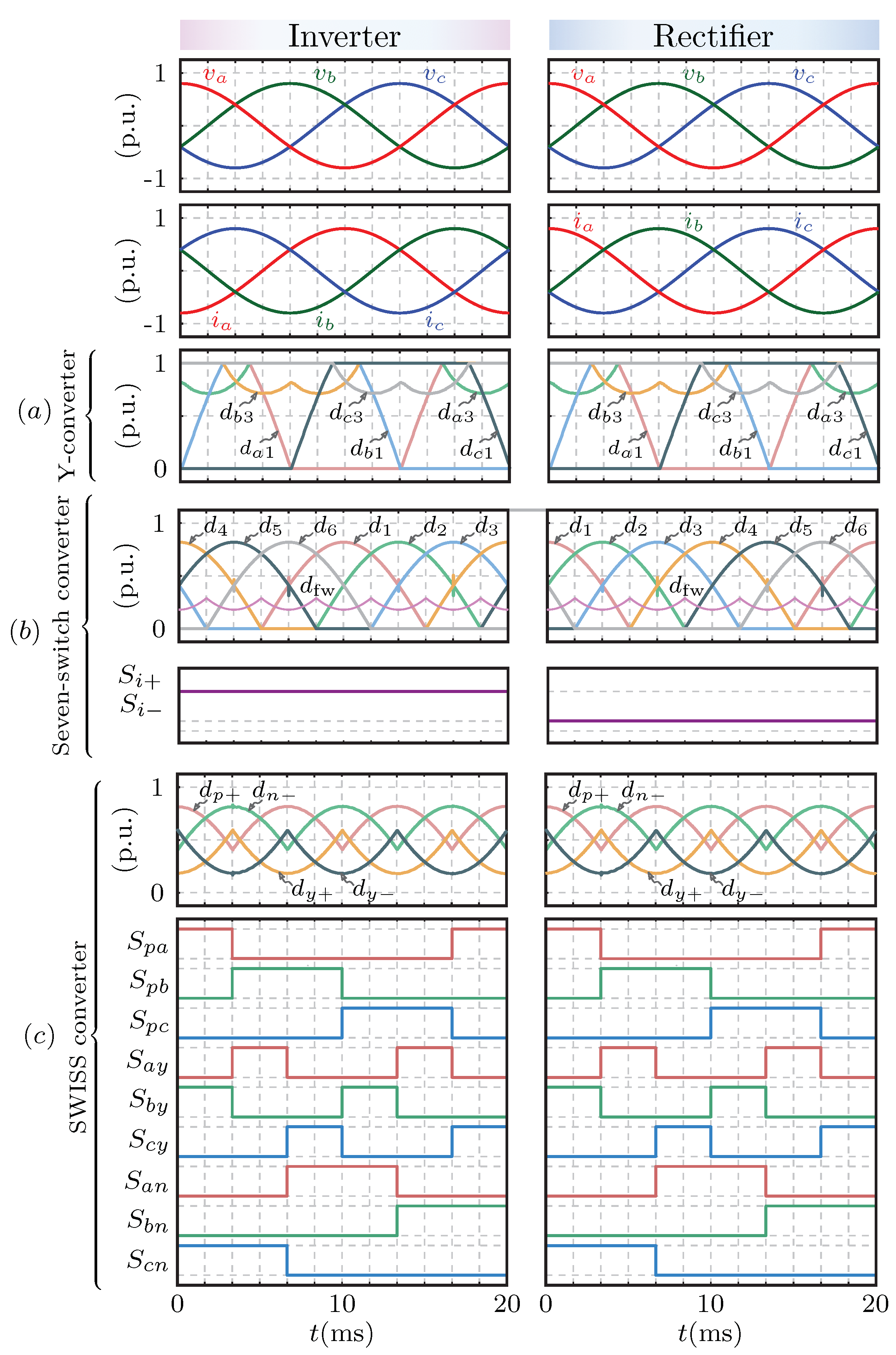
2. Topology Overview

In this section, a brief discussion is provided on the three topologies, along with an explanation of their operational principles and the driving pulse schemes employed by each converter.

2.1. Y-Converter

Figure 2a illustrates the Y-converter topology. In the standard representation, the Y-converter can be viewed as a conventional three-phase boost voltage source converter with an additional pre-stage to incorporate the buck feature. In the modular representation, the Y-converter is constructed by connecting three four-switch buck–boost DC-DC converters in a star configuration, all connected to a common point (m). For the sake of simplicity, the analysis in this paper will utilize the modular representation.
Since each module functions as a DC-DC converter, it is essential to ensure a positive input voltage at the AC input of the modules ( V { a , b , c } m must be kept 0 V ). To achieve this, a suitable offset voltage must be established between the grid neutrals (n) and (m). Different pulse-width modulation (PWM) techniques can be employed based on the selected offset voltage [26,28]. The PWM technique considered in this paper is the discontinuous PWM (DPWM), which provides a time-varying offset voltage represented by:
v o f f ( t ) = min ( v a ( t ) , v b ( t ) , v c ( t ) )
where v a , v b , and v c are the AC grid phase voltages.
The AC-side voltages ( v a m , v b m , and v c m ) of the three modules can be expressed as
v a m = V ^ m c o s ( ω t ) + v o f f v b m = V ^ m c o s ω t 2 π 3 + v o f f v c m = V ^ m c o s ω t + 2 π 3 + v o f f
where V ^ m is the peak value of the phase voltages.
In DPWM, the module with the most-negative grid voltage is clamped to point m. This clamping mode has the advantage of eliminating both semiconductor switching losses and inductor core losses for the clamped module, resulting in a significant reduction in overall losses. During the remaining part of the fundamental cycle, one half-bridge (either the buck or boost) is subjected to pulse width modulation, while the other half-bridge is clamped. The choice of modulation depends on whether the AC-side module voltage is higher or lower than the DC-side voltage. The Y-converter modulation and the duty cycles of the switches are depicted in Figure 3a.

2.2. Seven-Switch Buck Converter

The seven-switch buck converter comprises three main parts: a three-phase bridge, a freewheeling switch, and an inverting link. In this paper, the three-phase bridge is created using a series combination of SiC MOSFETs and SiC diodes that enable current flow in one direction and voltage blocking in both directions.
The converter operation is analyzed using space vector PWM (SVPWM) [16] and involves six active space vectors and a zero (null) space vector. The zero-space vector is achieved by activating only the freewheeling switch, whereas in the traditional six-switch topology, the entire leg is turned on. During the freewheeling state, the seven-switch converter has the advantage of the DC link current flowing through a single semiconductor device S f w , resulting in significantly reduced conduction losses compared to the four devices in the six-switch converter.
To enable bidirectional power capability, the inverting link is utilized to reverse the polarity of the DC-side voltage. In the rectification mode, the inverting link switches, such as S i + and S i , are turned off, allowing power transfer from the AC side to the DC side through D i + and D i . In the inversion mode, both S i + and S i are turned on, creating a negative DC link that facilitates power transfer from the DC side to the AC side. The seven-switch buck converter modulation and the duty cycles of the switches are presented in Figure 3b.

2.3. Swiss Converter

The Swiss converter is composed of three primary stages: an active three-phase bridge, a third harmonic injection network, and two buck DC-DC converters. The three-phase bridge functions as an uncontrolled rectifier bridge, driven to operate in a typical manner.
The third harmonic injection network includes three four-quadrant switches and is controlled to actively inject current solely into the phase with the lowest instantaneous voltage. Switching losses in both the active bridge and the injection network are neglected since they operate at the grid frequency and twice the grid frequency, respectively. When combined, the active bridge and the injection network form a three-phase unfolder. This three-phase AC unfolder converts the three-phase voltages into two DC voltages, namely v p y and v y n , which are utilized by the two buck DC-DC converters. This configuration enables the control of grid currents and the DC-side voltage by solely manipulating the duty cycle of the buck converters.
The duty cycles d p + of switch S p + and d n of switch S n are controlled in both the inverter and rectifier modes so that the AC-side current becomes sinusoidal. d p + and d n can be calculated as follows:
d p + = 2 3 V d c V ^ m 2 max ( v a , v b , v c ) d n = 2 3 V d c V ^ m 2 | min ( v a , v b , v c ) |
where V d c is the DC link voltage. The Swiss converter modulation and the duty cycles of the switches are presented in Figure 3c.

3. Analytical Power Loss Model

To assess and compare the three topologies, an analytical model is developed to calculate power losses. The model takes into account various types of power losses, including conduction losses in semiconductors, switching losses in semiconductors, copper losses, and core losses in inductors. Table 1 summarizes the converter parameters and the specific semiconductors used. The model is based on the following assumptions:
  • The inductances in all converters are assumed to be constant for the whole operating power range;
  • The comparison is held at a fixed junction temperature for all devices ( T j = 25 °C);
  • The reverse recovery losses of the SiC Schottky diode are neglected as a zero-reverse recovery current diode is utilized;
  • The input filter ( L f , C f ) is fixed for all topologies; the EMI filter is not considered.

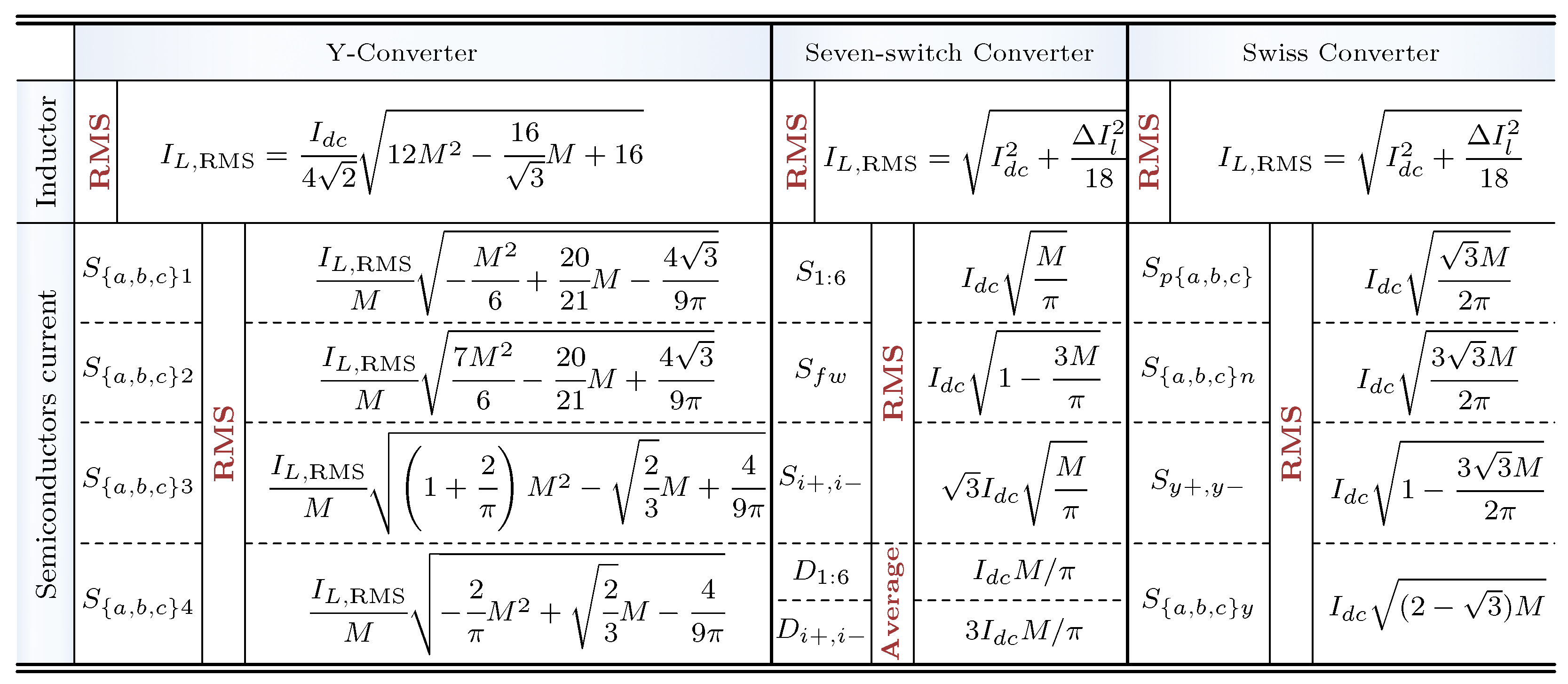
3.1. Semiconductor Conduction Losses

The conduction losses of power MOSFETs are calculated as follows:
P c o n d , s w = I D S , R M S 2 R D S , o n
where I D S , R M S is the RMS value of the MOSFET current, and these RMS values for the three topologies are summarized in Figure 4. R D S , o n is the on-state resistance of the power MOSFET and it is assumed to vary with the junction temperature T j according to the following equation:
R D S , o n ( m Ω ) = a 0 + a 1 T j + a 2 T j 2
The used fitting parameters for IMZ120R030M1H are:
a 0 = 29.78 m Ω , a 1 = 0.01556 m Ω / ° C , a 2 = 0.0009778 × 10 4 m Ω / ° C 2
For the SiC diodes in the seven-switch converter, the conduction losses are calculated as follows:
P c o n d , D = I D , r m s 2 R D , o n + I D , a v V D , o n
where I D , r m s and I D , a v are the RMS and the average values of the diode current, respectively. These values are summarized in Figure 4. R D , o n and V D , o n are the on-state resistance and the on-state voltage of the power diode and they are assumed to vary with the junction temperature T j , according to the following equations:
R D on ( m Ω ) = b 0 + b 1 T j V D on ( V ) = c 0 + c 1 T j
The used fitting parameters for C4D20120D are:
b 0 = 20 m Ω , b 1 = 0.266 m Ω / C , c 0 = 0.98 V , c 1 = 1.71 × 10 3 V / C

3.2. Semiconductors Switching Losses

The calculation of switching losses relies on the utilization of switching energy loss E s w versus drain-source current I D S curves of the SiC MOSFETs. These curves can be obtained from the manufacturer’s datasheet or through the implementation of a calorimetric switching loss measurement setup, as suggested in [29]. In this paper, two distinct polynomial fittings are employed to determine the turn-on energy loss E s w , o n and the turn-off energy loss E s w , o f f individually. This separation allows for easy integration of soft switching into the power loss model whenever it occurs. The polynomial fitting equations for E s w , o n and E s w , o f f are chosen to be fourth-order polynomials in order to minimize the root mean square error between the actual data and the fitted polynomials. The polynomial fitting equations can be expressed as:
E s w , on ( m J ) = V D S ( P 1 on I D S on 4 + P 2 on I D S on 3 + P 3 on I D S on 2 + P 4 on I D S on )
E s w , off ( m J ) = V D S ( P 1 off I D S off 4 + P 2 off I D S off 3 + P 3 off I D S off 2 + P 4 off I D S off )
where I D S , o n and I D S , o f f represent the instantaneous values of the MOSFET turn-on and turn-off currents, respectively, and V D S represents the instantaneous value of the MOSFET voltage. It is assumed that V D S remains constant during the turn-on and turn-off at every instant. The fitting parameters for IMZ120R030M1H are as follows:
P 1 on = 7.2730 × 10 10 A 3 . m s ; P 1 off = 5.4688 × 10 10 A 3 . m s P 2 on = + 7.0371 × 10 8 A 2 . m s ; P 2 off = + 5.2350 × 10 8 A 2 . m s P 3 on = 2.1250 × 10 6 A 1 . m s ; P 3 off = 1.4412 × 10 6 A 1 . m s P 4 on = + 3.6750 × 10 5 m s ; P 4 off = + 1.5450 × 10 5 m s
Given the switch voltage and current at the turn-on and turn-off instances, the switching energy is calculated using (10) and (11), then the switching losses are calculated.
In addition to the switching losses during the first quadrant operation of SiC MOSFETs, the power loss model includes switching losses during the third quadrant operation, i.e., the synchronous rectification mode. We assume that the turn-on switching losses in the synchronous rectifier mode are negligible, while at turn-off, power loss occurs due to the reverse recovery of the integral body diode. The switching energy losses due to reverse recovery ( E s w r r ) can be represented as functions of I d s and V s w [30] based on the following polynomial fitting:
The fitting parameters for IMZ120R030M1H are as follows:
E s w r r ( m J ) = V D S ( P 1 r r I s w o f f 2 + P 2 r r I s w o f f + P 3 r r )
P 1 r r = + 1.4037 × 10 8 A 1 . m s P 2 r r = + 1.1225 × 10 5 m s P 3 r r = + 2.8075 × 10 6 A . m s

3.3. Inductor Losses

The power inductor L is designed to provide the same inductor current ripple percentage at the rated power for all topologies ( Δ I L p = 20 % ). It can be calculated for the Y-converter as follows [28]:
L = V d c 8 2 Δ I L p I φ f s w
For the Swiss and seven-switch converters [13,20]:
L = V d c 2 Δ I L p I d c f s w 1 3 2 M
where M is the modulation index and can be expressed as follows:
M = 2 I φ ^ I d c = 2 3 V d c V m
where I d c is the DC-side current and I φ ^ is the RMS value of the AC-side phase current.
At the given M ( 0.8165 ) , previous equations result in almost the same value of L ( 190 μ H ) for the investigated topologies.
The power loss of L is divided into copper losses and core losses. For the copper losses, due to employing Litz wires to implement the inductor, skin effects and high-frequency losses can be neglected. Therefore, the copper losses are limited to the DC copper losses, which can be calculated as follows:
P c u = I L r m s 2 R L D C
where R L D C is the DC resistance of L.
The core loss is calculated based on the curve-fitting equations provided by the manufacturer [31]. The provided fitting equations represent experimentally measured magnetic property curves using closed-form equations. These equations facilitate the seamless integration of these magnetic properties into the power loss model. Starting from the maximum and minimum currents of the inductor at different instances, I L m a x , i , I L m i n , i , the corresponding values of magnetic flux intensity (H) and magnetic flux density (B) can be calculated as follows:
H = 0.4 π N I L 100 MPL
B = a + b H + c H 2 1 + d H + e H 2 x
where N is the number of turns, MPL is the magnetic path length in meters (m), H is in Oersted (Oe), and B is in Tesla (T). a, b, c, d, e, and x are the fitting parameters of the B-H curves provided by the manufacturer. The values of these fitting parameters are summarized in Table 2.
The core losses at a specific instant can be given by:
P c o r e = V c × a L o s s × ( B m a x B m i n ) b L o s s ( f s w 1000 ) c L o s s
where V c is the magnetic core volume in m 3 . a L o s s , b L o s s , and c L o s s are the fitting parameters for the core loss curves provided by the manufacturer. The inductor parameters along with the core loss fitting parameters are summarized in Table 2.

4. Comparative Analysis

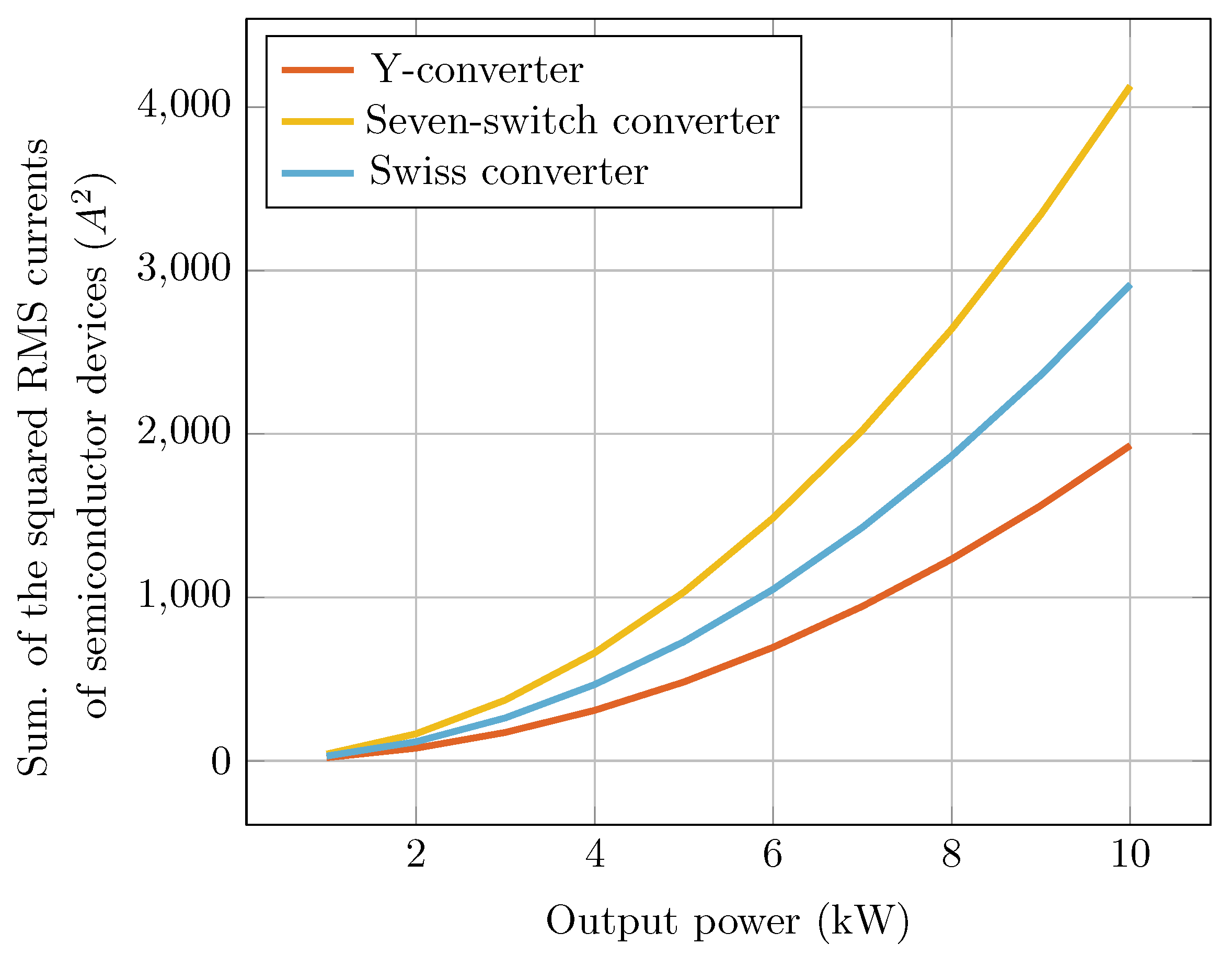
4.1. Semiconductors Stresses

4.1.1. Voltage Stresses

In the three topologies, the maximum voltage stress on semiconductor devices is represented by three distinct values: the peak line-to-line grid voltage ( 566 V ), the DC microgrid voltage ( 400 V ), and the voltage at the natural commutation points of the line-to-line grid voltage ( 537 V ). The 537 V peak voltage applies to the AC-side SiC MOSFETs ( S { a , b , c } 1 and S { a , b , c } 2 ) in the Y-converter, the three-phase bridge devices ( S 1 : 6 and D 1 : 6 ) in the seven-switch converter, and the three-phase bridge devices ( S 1 : 6 ) in the Swiss converter. The 400 V peak voltage is applicable to the remaining devices in the Y-converter and the seven-switch converter, while the 537 V peak voltage applies to the remaining devices in the Swiss converter. The voltage stresses of the three topologies are summarized in Figure 5.

4.1.2. Current Stresses

The formulas for the current stresses of the semiconductor devices in the three topologies are summarized in Figure 4. Additionally, The current stresses at 10 k W are summarized in Figure 5.
In order to provide deeper insight into the current stresses of the investigated topologies, the summation of the squared RMS currents of semiconductor devices in the investigated topologies are depicted in Figure 6. According to the obtained outcomes, the Y-converter exhibits the lowest summation across the entire power range. This implies that the Y-converter necessitates semiconductor devices with a lower current rating in comparison to the seven-switch and Swiss converters. Furthermore, if the same SiC devices are employed for all three topologies, the Y-converter will incur the least conduction losses at any given power level.

4.2. Semiconductors Losses

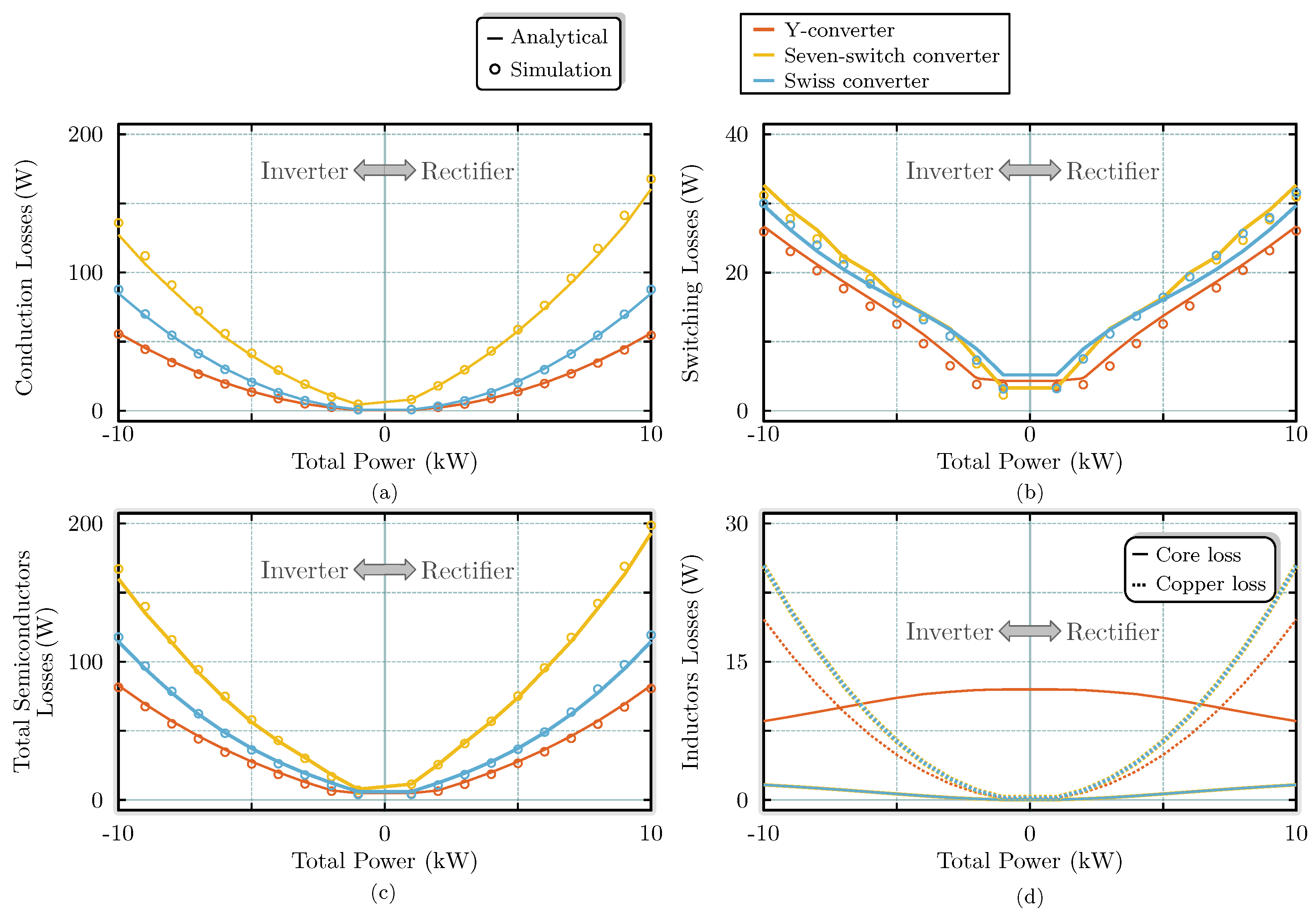
4.2.1. Conduction Losses

The conduction losses of the topologies are illustrated in Figure 7a. The Y-converter exhibits the lowest conduction losses throughout the entire operating range. This is primarily due to its minimal number of series switches in the current path for rectification and inversion. On the other hand, the seven-switch converter experiences the highest conduction losses. This can be attributed to the presence of SiC diodes and the excessive current stresses on the inverting link devices.

4.2.2. Switching Losses

The switching losses of the topologies are depicted in Figure 7b. In the Y-converter, the use of DPWM leads to a significant reduction in switching losses. Additionally, only a single leg in each module undergoes commutation at any given time, further contributing to lower losses. In the Swiss converter, although the switching losses are confined to the fast switches ( S p + and S n in the rectification mode and S y + and S y in the inversion mode), they are considerably high due to their operation under high currents. Given the semiconductor conduction and switching losses of the studied topologies, the total semiconductor losses are plotted in Figure 7c.

4.3. Inductor Losses

The inductor losses of the topologies are plotted in Figure 7d. Although the core losses in the Y-converter are reduced by employing DPWM, the Y-converter demonstrates the highest core losses among the studied topologies. The inductors in the Swiss converter and the seven-switch converters yield the same losses and sizes. The copper losses in the Y-converter are reduced as the total current is shared between the three phases, unlike the other topologies, where the total output current flows through the inductors.

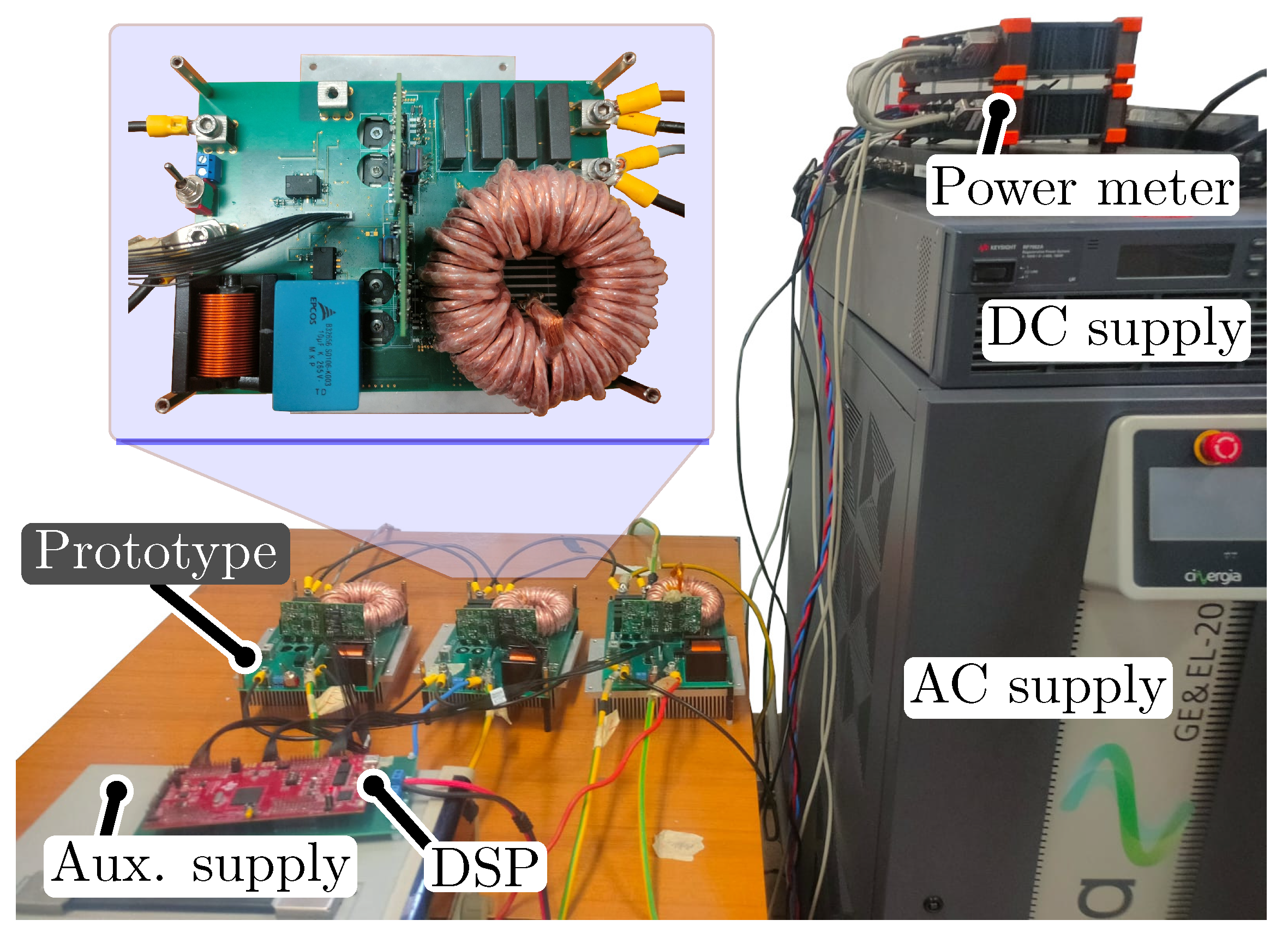
5. Experimental Results

To demonstrate the operation and high efficiency of the Y-converter, a 10 k W prototype of the Y-converter was implemented. The experimental setup is displayed in Figure 8. The experimental results are categorized as follows: key waveforms of the Y-converter, along with the measured THD of the AC side currents, and the measured efficiency of the converter, with its corresponding calculated power loss breakdown.

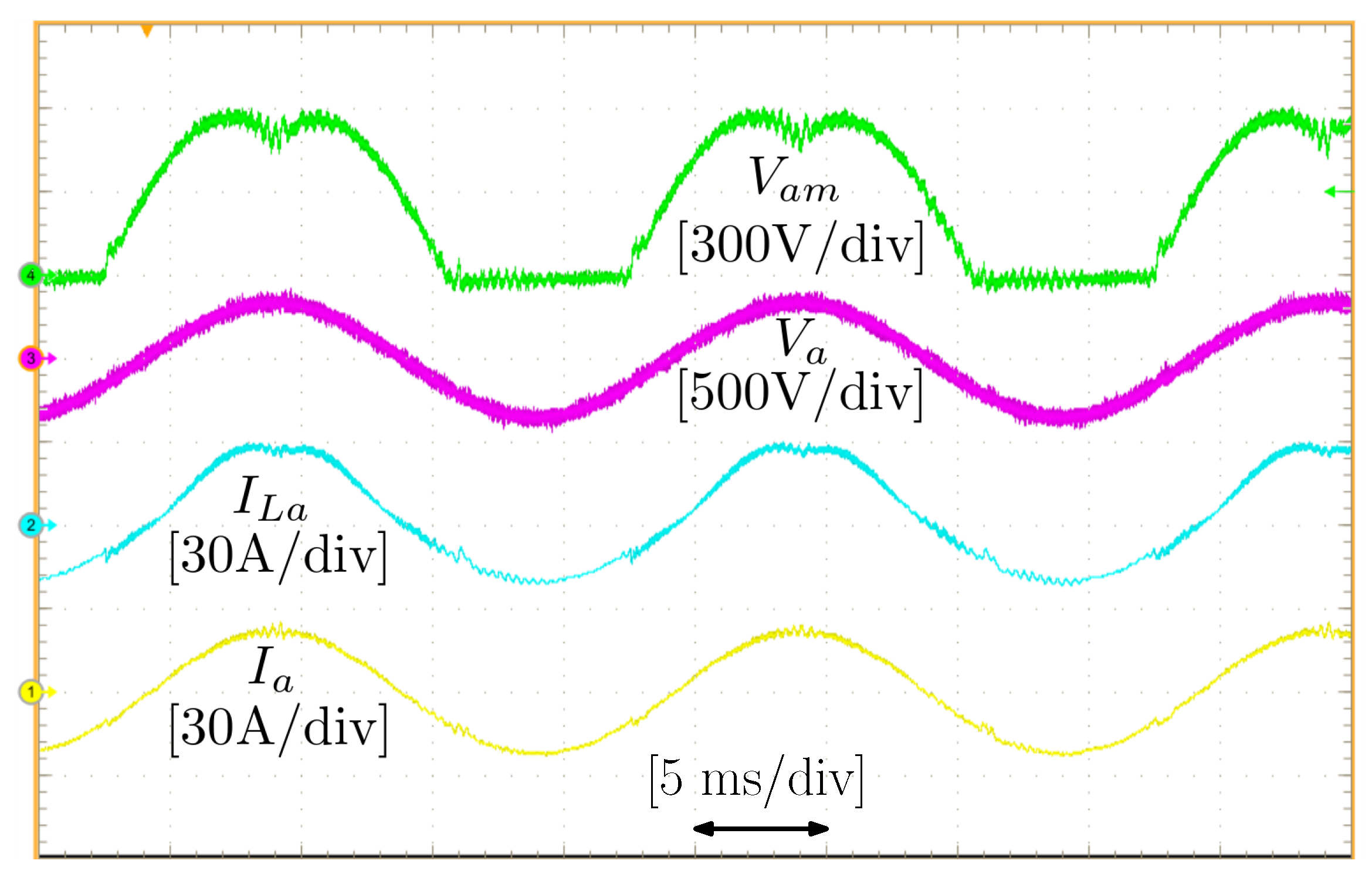
5.1. Key Waveforms and AC Current THDs

The selected key waveforms of the Y-converter are the AC-side voltage V a m , the grid voltage V a n , the inductor current I L a , and the grid current I a . Experimental results under full loads for both rectification and inversion modes are displayed in Figure 9 and Figure 10, respectively. The results show that the clamping mode is verified where V a m = 0 V , and I L a is shown to be ripple-free during clamping while preserving the sinusoidal shapes of both I L a and I a . The THDs of I a at different output power levels are presented in Figure 11 with 3.8% at the converter’s rated output power.

5.2. Measured Efficiency and Power Loss Breakdown

The efficiency of the prototype is measured using the Dewesoft SIRIUS XHS high-speed data acquisition (DAQ) system. The efficiency curve is plotted in Figure 11, which shows that the converter has a peak efficiency of 99.26% at nearly 40% of the rated power and 97.49% efficiency at the rated power.
Based on the previously discussed power loss model and the measured temperatures of the semiconductor devices during experimental tests, the calculated power loss breakdown for a half load and full load are displayed in Figure 12. At a half load, the semiconductor losses represent almost 60 % of the total losses with a roughly equalized distribution between conduction losses and switching losses. At a full load, the conduction loss contribution to the total losses is estimated to be 51 % , which explicitly means that using another SiC device with a lower R D S , o n can lead to better efficiency at a full load. The “other losses”, represented in the loss breakdown figure, is a generic term that represents the losses that are not included in the calculations, such as PCB losses, capacitor losses, etc., along with the mismatch between the calculated losses and the actual losses.

6. Discussion and Conclusions

This paper evaluates bidirectional step-down converters that enable the connection between the 400 V unipolar DC microgrid and the European low-voltage three-phase AC grid. The study compares three single-stage non-isolated topologies—the seven-switch buck converter, Swiss converter, and Y-converter—based on various factors, such as semiconductor stresses and losses, magnetic component sizes and losses, and heat sink sizes. The analysis is centered on a 10 k W converter that is suitable for residential or commercial use. The results indicate that the Y-converter has the lowest number of semiconductor devices, semiconductor device stresses, total losses, and heat sink sizes. The only drawback is that the total inductor size in the Y-converter is larger than those of the other studied topologies. Based on the findings, the Y-converter performs better overall than the other topologies, making it a potentially more suitable option for this application. A 10 k W Y-converter prototype is implemented and shown to have a peak efficiency of 99.26 % and an efficiency of 97.47 % at the rated output power. For future research, multi-objective optimization could be adopted for designing passive elements and selecting semiconductor devices. Subsequently, the topologies could be evaluated accordingly. This approach would offer a more comprehensive perspective on comparisons across various converter parameters, such as switching frequencies, inductor current ripples, and semiconductor device ratings. Additionally, investigating control strategies for each topology and evaluating their impacts on performances, losses, and efficiency could provide insight into the influence of these strategies on the converter’s behavior. This analysis would help identify opportunities for optimization.

Author Contributions

Formal analysis, A.Y.F., T.Y. and P.M.; writing—review and editing, D.B. All authors have read and agreed to the published version of the manuscript.

Funding

This work was supported by the Italian Ministry of Education, University, and Research under the following project: Holistic approach to EneRgyefficient smart nanOGRIDS (HEROGRIDS), grant PRIN 2017WA5ZT3.

Data Availability Statement

The most important data are included in the figures and tables, and the method is described so that no additional data are available.

Conflicts of Interest

The authors declare no conflict of interest.

Abbreviations

The following abbreviations are used in this manuscript:
PFCpower factor correction
SiCsilicon carbide
PWMpulse width modulation
DPWMdiscontinuous pulse width modulation
SVPWMspace vector pulse width modulation

References

  1. Kulasekaran, P.S.; Dasarathan, S. Design and Analysis of Interleaved High-Gain Bi-Directional DC-DC Converter for Microgrid Application Integrated with Photovoltaic Systems. Energies 2023, 16, 5135. [Google Scholar] [CrossRef]
  2. Murshed, M.; Chamana, M.; Schmitt, K.E.K.; Bhatta, R.; Adeyanju, O.; Bayne, S. Design and Performance Analysis of a Grid-Connected Distributed Wind Turbine. Energies 2023, 16, 5778. [Google Scholar] [CrossRef]
  3. Yan, S.; Gu, Z.; Park, J.H.; Xie, X. Adaptive Memory-Event-Triggered Static Output Control of T–S Fuzzy Wind Turbine Systems. IEEE Trans. Fuzzy Syst. 2022, 30, 3894–3904. [Google Scholar] [CrossRef]
  4. Yan, S.; Gu, Z.; Park, J.H.; Xie, X. Sampled Memory-Event-Triggered Fuzzy Load Frequency Control for Wind Power Systems Subject to Outliers and Transmission Delays. IEEE Trans. Cybern. 2023, 53, 4043–4053. [Google Scholar] [CrossRef] [PubMed]
  5. Pires, V.F.; Pires, A.; Cordeiro, A. DC Microgrids: Benefits, Architectures, Perspectives and Challenges. Energies 2023, 16, 1217. [Google Scholar] [CrossRef]
  6. Ali, S.; Zheng, Z.; Aillerie, M.; Sawicki, J.P.; Péra, M.C.; Hissel, D. A Review of DC Microgrid Energy Management Systems Dedicated to Residential Applications. Energies 2021, 14, 4308. [Google Scholar] [CrossRef]
  7. Kumar, D.; Zare, F.; Ghosh, A. DC Microgrid Technology: System Architectures, AC Grid Interfaces, Grounding Schemes, Power Quality, Communication Networks, Applications, and Standardizations Aspects. IEEE Access 2017, 5, 12230–12256. [Google Scholar] [CrossRef]
  8. Prabhala, V.A.; Baddipadiga, B.P.; Fajri, P.; Ferdowsi, M. An Overview of Direct Current Distribution System Architectures and Benefits. Energies 2018, 11, 2463. [Google Scholar] [CrossRef]
  9. Dragičević, T.; Lu, X.; Vasquez, J.C.; Guerrero, J.M. DC Microgrids—Part II: A Review of Power Architectures, Applications, and Standardization Issues. IEEE Trans. Power Electron. 2016, 31, 3528–3549. [Google Scholar] [CrossRef]
  10. Elsayed, A.T.; Mohamed, A.A.; Mohammed, O.A. DC microgrids and distribution systems: An overview. Electr. Power Syst. Res. 2015, 119, 407–417. [Google Scholar] [CrossRef]
  11. Justo, J.J.; Mwasilu, F.; Lee, J.; Jung, J.W. AC-microgrids versus DC-microgrids with distributed energy resources: A review. Renew. Sustain. Energy Rev. 2013, 24, 387–405. [Google Scholar] [CrossRef]
  12. Kolar, J.W.; Friedli, T. The Essence of Three-Phase PFC Rectifier Systems—Part I. IEEE Trans. Power Electron. 2013, 28, 176–198. [Google Scholar] [CrossRef]
  13. Stupar, A.; Friedli, T.; Minibock, J.; Kolar, J.W. Towards a 99% Efficient Three-Phase Buck-Type PFC Rectifier for 400-V DC Distribution Systems. IEEE Trans. Power Electron. 2012, 27, 1732–1744. [Google Scholar] [CrossRef]
  14. Baumann, M.; Kolar, J. Comparative evaluation of modulation methods for a three-phase/switch buck power factor corrector concerning the input capacitor voltage ripple. In Proceedings of the 2001 IEEE 32nd Annual Power Electronics Specialists Conference (IEEE Cat. No.01CH37230), Vancouver, BC, Canada, 17–21 June 2001; Volume 3, pp. 1327–1332. [Google Scholar] [CrossRef]
  15. Lorenzani, E.; Immovilli, F.; Migliazza, G.; Frigieri, M.; Bianchini, C.; Davoli, M. CSI7: A Modified Three-Phase Current-Source Inverter for Modular Photovoltaic Applications. IEEE Trans. Ind. Electron. 2017, 64, 5449–5459. [Google Scholar] [CrossRef]
  16. Wang, W.; Gao, F.; Yang, Y.; Blaabjerg, F. Operation and Modulation of H7 Current-Source Inverter with Hybrid SiC and Si Semiconductor Switches. IEEE J. Emerg. Sel. Top. Power Electron. 2018, 6, 387–399. [Google Scholar] [CrossRef]
  17. Vancu, M.F.; Soeiro, T.; Mühlethaler, J.; Kolar, J.W.; Aggeler, D. Comparative evaluation of bidirectional buck-type PFC converter systems for interfacing residential DC distribution systems to the smart grid. In Proceedings of the IECON 2012—38th Annual Conference on IEEE Industrial Electronics Society, Montreal, QC, Canada, 25–28 October 2012; pp. 5153–5160. [Google Scholar] [CrossRef]
  18. Soeiro, T.B.; Heldwein, M.L. Bidirectional three-phase PFC concept based on an integrated inverting-link current source converter. In Proceedings of the 2013 IEEE Energy Conversion Congress and Exposition, Denver, CO, USA, 15–19 September 2013; pp. 5137–5144. [Google Scholar] [CrossRef]
  19. Guo, B.; Wang, F.; Aeloiza, E. A novel three-phase current source rectifier with delta-type input connection to reduce the device conduction loss. IEEE Trans. Power Electron. 2016, 31, 1074–1084. [Google Scholar] [CrossRef]
  20. Soeiro, T.B.; Friedli, T.; Kolar, J.W. Design and Implementation of a Three-Phase Buck-Type Third Harmonic Current Injection PFC Rectifier SR. IEEE Trans. Power Electron. 2013, 28, 1608–1621. [Google Scholar] [CrossRef]
  21. Schrittwieser, L.; Leibl, M.; Haider, M.; Thöny, F.; Kolar, J.W.; Soeiro, T.B. 99.3% Efficient Three-Phase Buck-Type All-SiC SWISS Rectifier for DC Distribution Systems. IEEE Trans. Power Electron. 2019, 34, 126–140. [Google Scholar] [CrossRef]
  22. Schrittwieser, L.; Kolar, J.W.; Soeiro, T.B. Novel SWISS Rectifier Modulation Scheme Preventing Input Current Distortions at Sector Boundaries. IEEE Trans. Power Electron. 2017, 32, 5771–5785. [Google Scholar] [CrossRef]
  23. Chen, R.; Yao, Y.; Zhao, L.; Xu, M. Inhibiting mains current distortion for SWISS Rectifier—A three-phase buck-type harmonic current injection PFC converter. In Proceedings of the 2015 IEEE Applied Power Electronics Conference and Exposition (APEC), Charlotte, NC, USA, 15–19 March 2015; pp. 1850–1854. [Google Scholar] [CrossRef]
  24. Zhang, B.; Xie, S.; Li, Z.; Zhao, P.; Xu, J. An Optimized Single-Stage Isolated Swiss-Type AC/DC Converter Based on Single Full-Bridge with Midpoint-Clamper. IEEE Trans. Power Electron. 2021, 36, 11288–11297. [Google Scholar] [CrossRef]
  25. Soeiro, T.B.; Vancu, F.; Kolar, J.W. Hybrid Active Third-Harmonic Current Injection Mains Interface Concept for DC Distribution Systems. IEEE Trans. Power Electron. 2013, 28, 7–13. [Google Scholar] [CrossRef]
  26. Antivachis, M.; Bortis, D.; Schrittwieser, L.; Kolar, J.W. Three-phase buck-boost Y-inverter with wide DC input voltage range. In Proceedings of the 2018 IEEE Applied Power Electronics Conference and Exposition (APEC), San Antonio, TX, USA, 4–8 March 2018; pp. 1492–1499. [Google Scholar] [CrossRef]
  27. Farag, A.Y.; Younis, T.; Mattavelli, P.; Biadene, D. AC Grid-interface Bidirectional Buck-Type Converters for DC microgrids: A Comparative Study. In Proceedings of the IECON 2022—48th Annual Conference of the IEEE Industrial Electronics Society, Brussels, Belgium, 17–20 October 2022; pp. 1–6. [Google Scholar] [CrossRef]
  28. Antivachis, M.; Kleynhans, N.; Kolar, J.W. Three-Phase Sinusoidal Output Buck-Boost GaN Y-Inverter for Advanced Variable Speed AC Drives. IEEE J. Emerg. Sel. Top. Power Electron. 2020, 10, 3459–3476. [Google Scholar] [CrossRef]
  29. Rothmund, D.; Bortis, D.; Kolar, J.W. Accurate Transient Calorimetric Measurement of Soft-Switching Losses of 10-kV SiC mosfets and Diodes. IEEE Trans. Power Electron. 2018, 33, 5240–5250. [Google Scholar] [CrossRef]
  30. Sochor, P.; Huerner, A.; Hell, M.; Elpelt, R. Understanding the Turn-off Behavior of SiC MOSFET Body Diodes in Fast Switching Applications. In PCIM Europe Digital Days 2021; International Exhibition and Conference for Power Electronics, Intelligent Motion, Renewable Energy and Energy Management; Mesago Messe Frankfurt GmbH: Stuttgart, Germany, 2021; pp. 1–8. [Google Scholar]
  31. Magnetics Inc. Magnetics Powder Cores Catalog. 2020. Available online: https://www.mag-inc.com/Media/Magnetics/File-Library/Product%20Literature/Powder%20Core%20Literature/Magnetics-Powder-Core-Catalog-2020.pdf?ext=.pdf (accessed on 12 August 2023).
Figure 1. A bidirectional DC/AC converter connecting a DC microgrid to an AC grid.
Energies 16 06106 g001
Figure 2. The three buck-type converters. (a) Y-converter; (b) seven-switch converter; and (c) Swiss converter.
Energies 16 06106 g002
Figure 3. Modulation techniques for the three topologies. (a) Y-converter; (b) seven-switch converter; and (c) Swiss converter.
Energies 16 06106 g003
Figure 4. The current stresses of the different semiconductor devices in the three topologies.
Energies 16 06106 g004
Figure 5. Comparison between the three topologies in terms of the number of semiconductors, semiconductor stresses and losses, the size of the heat sink, and the magnetic element sizes.
Energies 16 06106 g005
Figure 6. Summation of the squared RMS currents of semiconductor devices of the studied topologies.
Energies 16 06106 g006
Figure 7. Comparison between the three topologies in terms of the semiconductor losses and inductor losses across the entire power operation range. Subfigures (ad) depict different loss components: conduction losses, switching losses, semiconductor losses, and inductor losses, respectively.
Energies 16 06106 g007
Figure 8. Picture of the Y-converter prototype.
Energies 16 06106 g008
Figure 9. Key waveforms of the rectification mode at rated power.
Energies 16 06106 g009
Figure 10. Key waveforms of the inversion mode at rated power.
Energies 16 06106 g010
Figure 11. Measured efficiency of the prototype.
Energies 16 06106 g011
Figure 12. Loss Breakdown.
Energies 16 06106 g012
Table 1. Three-phase PFC rectifier parameters.
ParameterSymbolValue
Converter parameters 1Nominal powerP10 k W
AC line voltageVac400 V
Line frequencyf50 Hz
Switching frequency f s w 62.5 k Hz
Output voltageVdc400 V
SiC MOSFETPart numberIMZ120R030M1H
VoltageVDS1200 V
Current I D 56 A
SiC DiodePart numberC4D20120D
VoltageVRRM1200 V
Current I F 66 A
Input FilterInductor L f 50 μ H
Capacitor C f 11.3 μ F
1 The converter parameters are utilized in both the evaluation of the converters and the experimental prototype.
Table 2. Inductor parameters.
ParameterSymbolValue
Inductor ParametersPart numberKoolMu 0079908A7
Magnetic path lengthMPL19.6 cm
Core volume V c 43.4 cm 3
Number of turnsN80Turns
Inductor DC resistance R L D C 20.3 m Ω
Fitting ParametersFlux density B
Equation (20)
a3.763 ×   10 2 T
b1.712 ×   10 2 T /Oe
c5.155 ×   10 4 T /Oe2
d9.190 ×   10 2 Oe−1
e4.909 ×   10 4 Oe−2
x1.812
Core losses P core
Equation (21)
a L o s s 52.36 J /( T . m 3)
b L o s s 1.988
c L o s s 1.541
Disclaimer/Publisher’s Note: The statements, opinions and data contained in all publications are solely those of the individual author(s) and contributor(s) and not of MDPI and/or the editor(s). MDPI and/or the editor(s) disclaim responsibility for any injury to people or property resulting from any ideas, methods, instructions or products referred to in the content.

